US8774580B2 - Turning mirror for photonic integrated circuits - Google Patents
Turning mirror for photonic integrated circuits Download PDFInfo
- Publication number
- US8774580B2 US8774580B2 US12/629,119 US62911909A US8774580B2 US 8774580 B2 US8774580 B2 US 8774580B2 US 62911909 A US62911909 A US 62911909A US 8774580 B2 US8774580 B2 US 8774580B2
- Authority
- US
- United States
- Prior art keywords
- light
- substrate
- turning mirror
- crystalline
- waveguide
- Prior art date
- Legal status (The legal status is an assumption and is not a legal conclusion. Google has not performed a legal analysis and makes no representation as to the accuracy of the status listed.)
- Active, expires
Links
Images


Classifications
-
- G—PHYSICS
- G02—OPTICS
- G02B—OPTICAL ELEMENTS, SYSTEMS OR APPARATUS
- G02B6/00—Light guides; Structural details of arrangements comprising light guides and other optical elements, e.g. couplings
- G02B6/24—Coupling light guides
- G02B6/42—Coupling light guides with opto-electronic elements
- G02B6/4201—Packages, e.g. shape, construction, internal or external details
- G02B6/4204—Packages, e.g. shape, construction, internal or external details the coupling comprising intermediate optical elements, e.g. lenses, holograms
- G02B6/4214—Packages, e.g. shape, construction, internal or external details the coupling comprising intermediate optical elements, e.g. lenses, holograms the intermediate optical element having redirecting reflective means, e.g. mirrors, prisms for deflecting the radiation from horizontal to down- or upward direction toward a device
-
- Y—GENERAL TAGGING OF NEW TECHNOLOGICAL DEVELOPMENTS; GENERAL TAGGING OF CROSS-SECTIONAL TECHNOLOGIES SPANNING OVER SEVERAL SECTIONS OF THE IPC; TECHNICAL SUBJECTS COVERED BY FORMER USPC CROSS-REFERENCE ART COLLECTIONS [XRACs] AND DIGESTS
- Y10—TECHNICAL SUBJECTS COVERED BY FORMER USPC
- Y10T—TECHNICAL SUBJECTS COVERED BY FORMER US CLASSIFICATION
- Y10T156/00—Adhesive bonding and miscellaneous chemical manufacture
- Y10T156/10—Methods of surface bonding and/or assembly therefor
Definitions
- the present disclosure is directed, in general, to an optical apparatus and more specifically, a photonic integrated circuit, and, methods of using and manufacturing the same.
- PIC photonic integrated circuit
- one embodiment is an optical device.
- the device comprises a substrate having a planar surface and an optical waveguide located on and parallel to the planar surface and having an end located and oriented to emit or receive light propagating substantially parallel to the planar surface.
- the device also comprises a crystalline turning mirror bound to the planar surface, the crystalline turning mirror having a bottom surface along the planar surface and having a reflecting surface that is slanted relative to said planar surface.
- the crystalline turning mirror and the substrate are formed of different materials.
- Another embodiment is a method of using an optical device.
- the method comprises transmitting light to an optical waveguide located on a planar surface of a substrate such that the light propagates substantially parallel to the planar surface.
- the method comprises emitting the transmitted light from an end of the waveguide, the end located and oriented to emit or receive the light.
- the method comprises reflecting the emitted light off of a reflecting surface of a crystalline turning mirror bound along a bottom surface thereof to the planar surface, the reflecting surface being slanted relative to the planar surface and oriented to direct the light into or out of the end of the waveguide.
- Another embodiment is a method of manufacturing an optical device.
- the method comprises forming an optical waveguide on a planar surface of a substrate, wherein the waveguide is parallel to the planar surface and an end of the waveguide is located and oriented to emit or receive light propagating substantially parallel to the planar surface.
- the method also comprises bonding a crystalline turning mirror to the planar surface, the bonded crystalline turning mirror having a reflecting surface that is slanted relative to the planar surface and is facing the end of the waveguide.
- FIGS. 1A-1D show plan and cross-sectional views of an example optical devices of the disclosure having at least one reflecting slanted surface
- FIGS. 2A-2B show plan and cross-sectional views of an example optical device of the disclosure having a plurality of reflecting slanted surfaces
- FIGS. 3A-3C show plan and cross-sectional views of example optical devices of the disclosure having one or more reflecting slanted surfaces and alignment features;
- FIGS. 4A-4B show plan and cross-section views of an example optical devices of the disclosure having at least one reflecting slanted surface
- FIGS. 5A-5C show plan and cross-section views of example optical devices of the disclosure having a photo-detector or light source optically coupled to a reflecting slanted surface of the device;
- FIGS. 6A-6C presents a flow diagrams of example methods of using an optical device in accordance with the disclosure, such as using any of the devices 100 discussed in the context of FIGS. 1A-5C ;
- FIGS. 7A-7B presents a flow diagram of example methods of manufacturing an optical device in accordance with the disclosure, such as any of the optical devices discussed in the context of FIGS. 1A-6B ;
- FIGS. 8A-16B present plan and cross-sectional views analogous to that shown in FIGS. 1A-5C , of selected steps in an example method of manufacturing of an example optical device in accordance with the disclosed method of manufacture, such as presented in the flow diagrams in FIGS. 7A or 7 B.
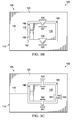
- FIGS. 1A and 1B show plan and cross-section views of an example optical device 100 of the disclosure.
- the device 100 can be, or include, a PIC 105 .
- the device 100 comprises a waveguide 110 and substrate 115 having a planar surface 120 .
- the optical waveguide 110 is located on and parallel to the surface 120 and having an end 122 located and oriented to emit or receive light propagating substantially parallel (e.g., direction 125 ) to the planar surface 120 .
- the substrate 115 can include cladding layers 130 , 132 to facilitate guiding light through the waveguide 110 .
- the device 100 also comprises a crystalline turning mirror 135 bound to the planar surface 120 .
- the crystalline turning mirror 135 has a reflecting surface 140 that is slanted relative to the planar surface 120 .
- the term turning mirror 135 as used herein refers to a structure having a least one reflecting surface 140 that reflects the light beam such that the beam's direction (e.g., direction 125 ) has been turned in a direction (e.g., direction 142 ) that is non-parallel to the incoming beam's direction 125 .
- the turning mirror 135 is a discrete physically separate structure.
- the turning mirror 135 and the substrate 115 (and any layers thereon) are discontinuous structures.
- the crystalline turning mirror 135 has a bottom surface 144 lying along a top surface 120 of the substrate 115 .
- slanted refers to the reflecting surface 140 forming an angle 146 with respect to the planar surface 120 , that ranges from about 30 to about 70 degrees.
- the substrate 115 , the waveguide 110 and the crystalline turning mirror 135 are components of a PIC 105 .
- the PIC 105 includes an array of the waveguides 110 and the crystalline turning mirrors 135 on the planar surface 120 .
- the device 100 is configured as an optical telecommunication system.
- the device 100 can be an optical telecommunication system that comprises a plurality of PICs 105 .
- the reflecting surface 140 is a planar reflecting surface.
- the reflecting surface 140 can be curved (e.g., concave or convex shaped).
- the reflecting surface 140 is covered by a metal layer 148 (e.g., gold).
- the crystalline turning mirror 135 and the substrate 115 are formed of different materials.
- the crystalline turning mirror 135 can be composed of silicon and the substrate 115 can be composed of glass.
- the reflecting surface 135 is desirable to have the reflecting surface 135 very close to the end 122 of the waveguide 110 because then the light being transferred between these two structures does not have the opportunity to substantially diverge. Consequently, a smaller sized detector can be used to detect the light.
- the reflecting surface 140 is separated from the end 122 by a distance 149 of about 20 micrometers or less.
- Some embodiments of the device 100 comprise a waveguide 110 and substrate 115 having a planar surface 120 .
- the optical waveguide 110 is located on and parallel to the surface 120 and having an end 122 located and oriented to emit or receive light propagating substantially parallel (e.g., direction 125 ) to the planar surface 120 .
- the device 100 also comprises a crystalline turning mirror 135 bound to the planar surface 120 .
- the crystalline turning mirror 135 has a reflecting surface 140 that is slanted relative to the planar surface 120 and a bottom surface 144 along the planar surface 120 .
- the crystalline turning mirror 135 and the substrate 115 are formed of different materials.
- FIGS. 1C and 1D show plan and cross-section views of another example optical device 100 of the disclosure.
- the optical device 100 comprises a PIC 105 that includes one or more optical waveguides 110 located on the substrate 115 .
- the waveguides 110 are configured to guide light in a direction 125 that is parallel to the planar surface 120 (e.g., a horizontal mounting surface) of the substrate 115 .
- the PIC 105 also includes one or more cavities 150 located on the substrate 115 .
- One end 122 of the waveguides 110 terminates at an interior wall 152 of one of the cavities 150 .
- At least a portion of the crystalline turning mirror 135 is located in a cavity 150 on the planar surface 120 . Mounting the turning mirror 135 in the cavity 150 can facilitate producing an optical device 100 with a low vertical profile. Consequently, the assembly of such devices 100 are more conducive to mass-assembly processes, such as flip-chip assembly processes. In some embodiments at least a portion of the crystalline turning mirror 135 is part of a cavity 150 of an optical resonator located on the planar surface 120 .
- each of the turning mirrors 135 fits into one of the cavities 150 . That is, the shape of the portion of the turning mirror 135 (or entire mirror in some cases) can fit in one of the cavities 150 because it matches or conforms with the shape of the cavity 150 and is slightly smaller than the cavity 150 .
- At least one sidewall 155 of each of the turning mirrors 135 has a reflecting surface 140 facing the end 122 of one of the waveguides 110 .
- the reflecting surface 140 is slanted relative to the planar surface 120 .
- the reflecting surface 140 is configured to reflect the light emanating from the waveguide 110 and into the cavity 150 in a direction (e.g., direction 142 ) that is non-parallel to the planar surface 120 . In other embodiments of the device 100 , the reflecting surface 140 is configured to reflect the light emanating from a direction (e.g., direction 142 ) that is non-parallel with the planar surface 120 to a direction 125 that is planar surface 120 and into the waveguide 110 .
- FIGS. 2A and 2B show plan and cross-section views of another example optical device 100 of the disclosure.
- all of the sidewalls 155 , 210 , 215 , 220 of the turning mirrors 135 have substantially identical slanted reflecting surfaces 140 .
- An advantage of such a configuration is that it ensures that the reflecting surface 140 will face the end 122 of the waveguide 110 , regardless of how the turning mirror 135 is horizontally oriented in the cavity 150 .
- FIG. 3A shows a plan view of yet another example optical device 100 of the disclosure.
- the sidewall 155 of at least one turning mirror 135 further includes a second reflecting surface 305 , that is separated from the reflecting surface 140 , and, the second reflecting surface 305 faces a second one of the waveguides 310 .
- each one of the turning mirrors 135 can have a plurality of such, separated reflecting surfaces 140 , 305 .
- the shape of the turning mirrors 135 in a plane parallel to the planar surface 120 is configured to match a shape of the cavity. For instance, as illustrated in FIG. 1C , in some cases when the cavity 150 is rectangular-shaped, then the shape of the turning mirror 135 has a matching rectangular shape in the plane of the planar surface 120 . In some cases, the cavity's shape, and the corresponding shape of the turning mirror, could be configured to have an asymmetric shape such that the turning mirror can only fit in the cavity in one orientation, such that the reflecting surface faces the waveguide.
- At least one of the interior walls or a base (e.g., interior walls 152 or base 157 as depicted in FIG. 1D ) of the cavity includes one or more alignment-features, and, at least one side of the turning mirror includes corresponding alignment-features which fit the alignment-features.
- the alignment feature projects out from the interior wall or base of the cavity
- the corresponding alignment feature projects into the turning mirror by a substantially equal and opposite amount.
- two opposing interior walls 152 of the cavity 150 have v-shaped notches outward-projecting alignment features 315
- two side walls 155 having corresponding v-shaped inward-projecting notch alignment features 320
- the cavity's alignment features 315 and the corresponding turning mirror's alignment features 320 are notches having other shapes (e.g., square, hemisphere, etc. . . . . ).
- the one or more alignment-features 315 can have a variety of shapes that either projects into or out of one or more of the interior walls 152 , and, how the corresponding alignment-feature 320 of the turning mirror 135 can have an inverse or complimentary shape that either projects out of or into the sidewall 155 , respectively.
- the alignment features 315 on the interior walls 152 can project inwards while the corresponding alignment features 320 on the sidewalls 155 project outwards.
- the alignment-features can be asymmetrically shaped or asymmetrically positioned on the interior walls 152 . This helps to ensure that the reflecting surface 140 will face the waveguide 110 .
- FIG. 3B shows a plan view of still another example optical device 100 of the disclosure.
- one of the interior walls 152 (or base in other embodiments) has a first alignment feature 330 (e.g., an inward projecting notch) and another one of the interior walls 152 (or base) has a differently-shaped alignment feature 332 (e.g., an outward projecting notch).
- the turning mirror 135 includes corresponding alignment features, 335 , 337 .
- the turning mirrors include one or more tethering remnants on one or more sidewalls 155 or bottom surface 144 ( FIG. 1D ) of the turning mirror.
- tethers can be used in the fabrication of the turning mirror to hold the mirror to a substrate while the mirror is being formed from the substrate. Once the mirror is formed, the tethers can be broken, leaving tethering remnants on the mirror's sidewalls or base.
- Example tethering remnants are illustrated in FIG. 3C which shows a plan view of another example optical device 100 of the disclosure. As illustrated, side walls 155 (or the bottom surface 144 , FIG.
- the turning mirror can be configured such that the alignment features 342 and corresponding alignment-features 340 of the turning mirror 135 , are asymmetrically positioned, on the interior walls 152 and side walls 155 , respectively, to facilitate the desired orientation of the reflecting surface 140 to face the end 122 of the waveguide 110 .
- the turning mirrors can include one or more etch release holes.
- etch release holes can be used in the fabrication of the turning mirror to facilitate releasing the mirror from a substrate that the mirror is manufactured from.
- the etch release holes can be used as alignment features.
- FIGS. 4A and 4B show plan and cross-section views, respectively, of yet another embodiment of the optical device 100 .
- One or more etch release holes 410 are located on a bottom surface 144 of the turning mirror 135 . As shown in FIG. 4B , the etch release holes 410 can vertically traverse the mirror 135 .
- the etch release holes 410 can be corresponding alignment-features for alignment features 415 (e.g., outward projecting posts) on the cavity base 157 .
- FIGS. 5A and 5B show plan and cross-sectional views, respectively, of the device 100 which can further include one or more photo-detectors 510 located on the planar surface 120 .
- Each photo-detector 510 can be configured to receive light reflected from one of the reflecting surfaces 140 turning mirrors 135 .
- the light sensor 515 of the photo-detector 510 e.g., a photodiode
- the waveguide 110 e.g., in direction 125
- FIG. 5C shows a cross-sectional view, analogous to that shown in FIG. 5B , of another embodiment of the device 100 further including a light-source 520 (e.g., laser or optical fiber) which directs the light in a direction (e.g., direction 142 ) that is non-parallel to the planar surface 120 , towards the reflecting surfaces 140 .
- the light reflected off of the reflecting surface travels in a direction (e.g., direction 125 ) parallel to planar surface 120 into the waveguide 110 .
- FIG. 6A presents a flow diagram of an example method of using an optical device in accordance with the disclosure, such as using any of the devices 100 discussed in the context of FIGS. 1A-5C .
- the method comprises a step 610 of directing a light through an optical waveguide 110 located on a planar surface 120 of a substrate 115 , wherein the light propagates substantially parallel to the planar surface (e.g., in direction 125 ).
- the method also comprises a step 615 of directing the light through an end 122 of the waveguide 110 , the end 122 located and oriented to emit or receive the light.
- the method further comprises a step 620 of reflecting the light off of a reflecting surface 140 of a crystalline turning mirror 135 bound to the planar surface 120 , the reflecting surface 140 being slanted relative to the planar surface 120 and oriented to direct the light (e.g., direction 125 ) into or out of the end 122 of the waveguide 110 .
- the light directed through the end 122 of the waveguide 110 is then reflected off of the reflecting surface 140 in a direction 142 that is non-parallel to the planar surface 120 .
- the reflected light can then be received by a photo-detector 510 ( FIG. 5A ) located on the planar surface 120 .
- the light reflected off of the reflecting surface 140 is in a direction 125 that is parallel to the planar surface 120 and into the end 122 of the waveguide 110 .
- the light can be directed (e.g., in direction 142 ) toward the reflecting surface 140 from a light-source 520 ( FIG. 5C ) located above the planar surface 120 .
- FIG. 6B presents a flow diagram of another example method of using an optical device in accordance with the disclosure, such as using any of the devices 100 discussed in the context of FIGS. 1A-5C .
- the method comprises a step 630 of transmitting a light in a photonic integrated circuit 105 .
- Transmitting the light in step 630 includes a step 632 of directing the light (e.g., in direction 125 ) through one or more waveguides 110 located on a planar surface 120 of a substrate 115 of the circuit 105 .
- directing the light in step 632 can include transmitting the light to the waveguide 110 .
- Transmitting the light in step 630 includes a step 634 of directing the light (e.g., in direction 142 ) through an end 122 of the waveguides 110 that terminate at an interior wall 152 of one or more cavities 150 of the substrate 115 .
- directing the light in step 634 can include emitting light from the end 122 of the waveguide 110 .
- Transmitting the light in step 630 also includes a step 636 of reflecting the light off of a reflecting surface 140 of a sidewall 155 of one or more of the turning mirrors 125 of the circuit 105 (e.g., any of the turning mirrors discussed in the context of FIGS. 1A-5C ).
- the light directed through the end 122 of the waveguide 110 in step 634 is then reflected off of the reflecting surface 140 , in step 636 , in a direction 142 that is non-parallel to the planar surface 120 .
- the light reflected off the reflecting surface in step 636 can then be received, in step 638 , by a photo-detector 510 located on said planar surface 120 .
- the light reflected off of the reflecting surface 140 in step 636 is reflected in a direction that is parallel to said planar surface and the end 122 of one of the waveguides in step 634 .
- the light can be directed in step 640 from above the planar surface 120 towards the reflecting surface 140 .
- the light in step 640 can emanate directly from a light-source 520 (not shown), such as a laser or optical fiber, that is pointed at the reflecting surface.
- the light can emanate indirectly in step 640 from another turning mirror located on the mounting surface 120 (not shown) that in turn receives light from the light-source 520 and direct the light down to the turning mirror 135 .
- FIG. 6C presents a flow diagram of another example method of using an optical device in accordance with the disclosure, such as using any of the devices 100 discussed in the context of FIGS. 1A-5C .
- the method comprises a step 650 of transmitting light to an optical waveguide 110 located on a planar surface 120 of a substrate 115 such that the light propagates substantially parallel to the planar surface 120 (e.g., in direction 125 ).
- the method also comprises a step 652 of emitting the transmitted light from an end 122 of the waveguide 110 , the end 122 located and oriented to emit or receive the light.
- the method further comprises a step 654 of reflecting the light off of a reflecting surface 140 of a crystalline turning mirror 135 bound along a bottom surface 144 thereof to the planar surface 120 , the reflecting surface 140 being slanted relative to the planar surface 120 and oriented to direct the light (e.g., direction 125 ) into or out of the end 122 of the waveguide 110 .
- the light emitted from the end 122 of the waveguide 110 is reflected off of the reflecting surface 140 in a direction 142 that is non-parallel to the planar surface 120 .
- the light can be directed (e.g., in direction 142 ) toward the reflecting surface 140 from a light-source 520 ( FIG. 5C ) located above the planar surface 120 .
- FIG. 7A presents a flow diagram of an example method of manufacturing an optical device in accordance with the disclosure, such as any of the optical devices discussed in the context of FIGS. 1A-6C .
- the method embodiment depicted in FIG. 7A comprises a step 705 of forming an optical waveguide 110 on a planar surface 120 of a substrate 115 .
- the waveguide 110 is parallel to the planar surface 120 and an end 122 of the waveguide 110 is located and oriented to emit or receive light propagating substantially parallel to the planar surface 120 (e.g., in direction 125 ).
- the method also comprises a step 710 of bonding a crystalline turning mirror 135 to the planar surface 120 .
- the crystalline turning mirror 135 (e.g., the bonded mirror) has a reflecting surface 140 that is slanted relative to the planar surface 120 and the reflecting surface 140 faces the end 122 of the waveguide 110 .
- the method further includes a step 715 of forming a cavity 150 (e.g., an optical resonant cavity) on the planar surface 120 wherein the end 122 of the waveguide 110 terminates at an interior wall 152 of the cavity 150 and at least a portion of the crystalline turning mirror 135 is located in the cavity 150 .
- a cavity 150 e.g., an optical resonant cavity
- At least a portion of the crystalline turning mirror 135 is located along a wall 152 of the cavity 150 .
- the method further includes a step 720 of patterning a second substrate to form the crystalline tuning mirror 135 . In some cases, the method further includes a step 725 of etching a second substrate to form the slanting reflecting surface 140 .
- FIG. 7B presents a flow diagram of another example method of manufacturing an optical device in accordance with the disclosure, such as any of the optical devices discussed in the context of FIGS. 1A-6B .
- the method embodiment depicted in FIG. 7B comprise a step 725 of forming a PIC 105 .
- Forming the PIC 105 includes a step 735 of forming one or more waveguide 110 on a planar surface 120 of a substrate 115 , and, a step 740 forming one or more cavities 150 on the substrate 115 ( FIGS. 1C-1D ), such that one end 122 of waveguides 110 terminates at an interior wall 152 of the cavity 150 .
- Forming the PIC 105 (step 725 ) also includes a step 745 of providing one or more turning mirrors 135 , each having at least one sidewall 155 with a reflective surface 140 .
- Forming the PIC 105 further includes a step 750 of mounting at least a portion of at least one of the turning mirrors 135 into one of the cavities 150 .
- Mounting is done such that the reflective surface 140 faces the waveguide's 110 end 122 , and such that the reflecting surface 140 is slanted relative to the planar surface 120 .
- Forming the waveguide 110 in step 735 and the cavities 150 in step 740 can both include photolithographic patterning and etching processes that are well known to those skilled in the art.
- forming the cavities 150 (step 740 ) includes a step 755 of patterning the substrate 115 such that at least one interior wall 152 or base 157 of the cavity further includes at least one alignment feature (e.g., one or more features 320 , 335 , 337 , 342 , 415 of FIGS. 1A-4B ).
- providing the turning mirror 135 (step 745 ) further includes a step 760 of patterning a second substrate such that at least the mounting portion of the turning mirror 135 has a shape that fits in one of the cavities 150 .
- the patterning step 760 further includes a step 765 of forming an alignment feature (e.g., one or more corresponding features 315 , 335 , 337 , 340 , 410 of FIGS. 1A-4B ) in one or more sidewalls 155 or bottom surface 144 of the mounting portion that corresponds to the alignment feature on the interior wall 152 or base 157 of one of the cavities 150 , when the turning mirror 135 is mounted in the cavity 150 .
- the patterning step 760 further includes a step 767 of forming release holes 410 ( FIG. 4A-4B ) in the turning mirror 135 .
- providing the turning mirror 135 ( 745 ) further includes a step 770 of etching a second substrate to form at least one sidewall 155 with a slanted surface (e.g., the sidewall 155 having an the angle 146 relative to the planar surface 120 ; FIG. 1B ).
- the patterning step 760 (including step 765 ) to be done before the etching step 770 to form the slanted surface.
- RIE reactive ion etching
- the patterned second substrate is more conducive to further photolithographic processing than the etched second substrate because the former can have a more uniformly planar surface.
- providing the turning mirror ( 745 ) further includes a step 775 of coating the slanted reflecting surface 140 with a reflective layer 142 (e.g., via metal evaporation processes).
- providing the turning mirror ( 745 ) further includes a step 780 of releasing a patterned layer of a second substrate.
- hydrofluoric acid etchant can be transferred through release holes 410 ( FIG. 4A ) in the patterned layer of the second substrate to dissolve a layer of the second substrate, thereby releasing the patterned turning mirror 135 .
- FIGS. 8A-16B present plan and cross-sectional views analogous to that shown in FIGS. 1A and 1B , respectively, of selected steps in an example method of manufacturing of an example optical device 100 in accordance with the disclosed method of manufacture, such as presented in the flow diagrams in FIGS. 7A or 7 B.
- FIGS. 8A and 8B show an example substrate 115 of the device 100 , such as a silicon substrate, having a silicon base layer 805 , lower layer 810 (e.g., silicon oxide) and core layer 815 (e.g., glass).
- a silicon base layer 805 having a silicon base layer 805 , lower layer 810 (e.g., silicon oxide) and core layer 815 (e.g., glass).
- core layer 815 e.g., glass
- FIGS. 9A and 9B show the device 100 after patterning the substrate 115 to form a waveguide 110 , e.g., as part of step 705 ( FIG. 7A ) or step 735 ( FIG. 7B ).
- the lower layer 810 of silicon oxide acts as a cladding layer for the waveguide 110 (e.g., composed of silicon).
- FIGS. 9A and 9B also shows the device 100 after covering the waveguide 110 with an upper layer 910 also as part of step 710 or step 735 .
- an upper layer 910 e.g., composed of a second type of glass, can be blanket-deposited over the entire substrate 115 via physical or vapor deposition processes.
- the upper layer 910 of glass acts as a cladding layer for the waveguide 110 .
- FIGS. 10A and 10B show the device 100 after patterning the substrate 115 to form a cavity 150 , e.g., as part of step 715 ( FIG. 7A ) or step 740 ( FIG. 7B ).
- it is desirable to form the cavity 150 in step 740 after forming the waveguide 110 because this facilitates forming the cavity such that the end 122 of the waveguide 110 terminates at an interior wall 152 of the cavity 150 .
- only the upper and lower layers 810 , 910 are patterned as forming the cavity 150 .
- the base substrate layer 805 could also be patterned.
- the patterning step can further include forming an alignment feature (e.g., analogous to one or more corresponding features 315 , 335 , 337 , 340 , 410 of FIGS. 1A-4B ) in accordance with step 755 .
- an alignment feature e.g., analogous to one or more corresponding features 315 , 335 , 337 , 340 , 410 of FIGS. 1A-4B .
- FIGS. 11A and 11B show the device 100 after providing a turning mirror 135 , e.g., as part of step 745 .
- FIGS. 12A and 12B shows the device 100 after mounting the turning mirror 135 in the cavity 150 , in accordance with step 750 ( FIG. 7B ).
- mounting the turning mirror 135 includes bonding the turning mirror 135 (e.g., the bottom surface 144 ) to the substrate's 115 mounting surface 120 (e.g., the base 157 of the cavity 150 ) using an adhesive 1210 , such as an adhesive designed specifically for chip bonding in microelectronic and optoelectronic applications. Examples include conductive epoxy adhesives such as Epotek H20E (Epoxy Technology, Inc., Billerica, Mass.).
- the turning mirror 135 is bound to the substrate surface 120 in accordance with step 710 ( FIG. 7A ) in the absence of a cavity 150 .
- suitable mounting techniques such as the use of robotically-controlled micro-manipulators to mount the turning mirror 135 , or a portion thereof, in the cavity 150 (e.g., FIGS. 1C-1D ) or bound the turning mirror 135 to the surface 120 which does not have a cavity (e.g., FIGS. 1A-1B ).
- FIGS. 13A-16B show selected steps in an example process of providing a turning mirror 135 in accordance with step 745 .
- FIGS. 13A and 13B show a second substrate 1310 from which the turning mirror 135 can be fabricated from.
- the second substrate 1310 is a silicon-on-insulator substrate, having an underlying material layer 1315 of silicon oxide and upper material layer 1320 of silicon.
- FIGS. 13A and 13B also show the second substrate 1310 after patterning (e.g., step 720 , FIG. 7A ; step 760 , FIG. 7B ) as part of forming the turning mirror 135 .
- patterning e.g., step 720 , FIG. 7A ; step 760 , FIG. 7B
- standard photolithography and etching e.g., reactive ion etching
- the pattern step 760 can further include forming alignment feature 1330 and release holes 1335 in the second substrate 1310 , in accordance with steps 765 and 767 , respectively.
- FIGS. 14A and 14B show the second substrate 1310 after being etched to form a slanting reflecting surface 1410 (e.g., slanting relative to a planar surface 1420 ), in accordance with step 710 ( FIG. 7A ) or step 770 ( FIG. 7B ).
- a slanting reflecting surface 1410 e.g., slanting relative to a planar surface 1420
- at least one sidewall 155 of the turning mirror 135 can be etch to form a slanted surface 1410 relative to a planar surface 1420 which can include a non-etched top surface of the material layer 1320 of the second substrate 1310 .
- the material layer 1320 when the material layer 1320 is a crystalline layer (e.g., a (100) silicon layer), a portion of the material layer 1320 can be etched to form a slanted second trench 1430 along the sidewall 155 , using an anisotropic etch, such as a wet potassium hydroxide (KOH) etch.
- KOH wet potassium hydroxide
- FIGS. 15A and 15B show the second substrate 1310 after coating the slanted surface 1410 ( FIG. 1410 ) of the turning mirror 135 with a reflective layer 1510 , e.g., in accordance with step 775 ( FIG. 7B ) as part of forming the reflecting surface 140 .
- a reflective layer 1510 of metal such as gold can be deposited via a metal evaporation process.
- the material layer 1320 is made of a reflective material (e.g., a metal such as gold, silver, aluminum, or metal alloys) there may be no need to coat the slanted surface 1410 with the reflective layer 1510 .
- FIGS. 16A and 16B shows the turning mirror 135 after being released from the second substrate 1310 ( FIGS. 15A and 15B ) in accordance with step 780 .
- the turning mirror 135 can be released by introducing an etchant such as hydrofluoric acid through the trenches 1315 , 1430 ( FIGS. 15A and 15B ) and release holes 1330 to thereby dissolve portions of the underlying layer 1330 that hold the turning mirror 135 to the substrate 1310 .
- an etchant such as hydrofluoric acid
- the turning mirror 135 is partially released from the second substrate 1310 prior to coating the slanted surface 1410 as described above.
- the turning mirror 135 can be tethered to the second substrate 1310 but otherwise released from the underlying layer 1315 of the second substrate 1310 ( FIG. 13B ).
- the turning mirror 135 can be fully released by breaking the tethers.
- the process of breaking the tethers can leave tethering remnants on the turning mirror 135 , which in turn, can be used as alignment features (e.g., tethering remnants 340 FIG. 3C ).
- One skilled in the art would be familiar with other steps that could be performed to form other components of the optical device, including forming or providing photo detectors, light-source, such as a laser light-source, to complete the optical device, e.g., to be, or to include a PIC 105 .
Abstract
Description
Claims (13)
Priority Applications (1)
| Application Number | Priority Date | Filing Date | Title |
|---|---|---|---|
| US12/629,119 US8774580B2 (en) | 2009-12-02 | 2009-12-02 | Turning mirror for photonic integrated circuits |
Applications Claiming Priority (1)
| Application Number | Priority Date | Filing Date | Title |
|---|---|---|---|
| US12/629,119 US8774580B2 (en) | 2009-12-02 | 2009-12-02 | Turning mirror for photonic integrated circuits |
Publications (2)
| Publication Number | Publication Date |
|---|---|
| US20110129181A1 US20110129181A1 (en) | 2011-06-02 |
| US8774580B2 true US8774580B2 (en) | 2014-07-08 |
Family
ID=44068974
Family Applications (1)
| Application Number | Title | Priority Date | Filing Date |
|---|---|---|---|
| US12/629,119 Active 2031-09-06 US8774580B2 (en) | 2009-12-02 | 2009-12-02 | Turning mirror for photonic integrated circuits |
Country Status (1)
| Country | Link |
|---|---|
| US (1) | US8774580B2 (en) |
Cited By (4)
| Publication number | Priority date | Publication date | Assignee | Title |
|---|---|---|---|---|
| US11022755B2 (en) | 2018-10-23 | 2021-06-01 | Cudoquanta Florida, Inc. | Demountable edge couplers with micro-mirror optical bench for photonic integrated circuits |
| US11437308B2 (en) | 2019-03-29 | 2022-09-06 | Absolics Inc. | Packaging glass substrate for semiconductor, a packaging substrate for semiconductor, and a semiconductor apparatus |
| US11469167B2 (en) | 2019-08-23 | 2022-10-11 | Absolics Inc. | Packaging substrate having electric power transmitting elements on non-circular core via of core vias and semiconductor device comprising the same |
| US11652039B2 (en) * | 2019-03-12 | 2023-05-16 | Absolics Inc. | Packaging substrate with core layer and cavity structure and semiconductor device comprising the same |
Families Citing this family (8)
| Publication number | Priority date | Publication date | Assignee | Title |
|---|---|---|---|---|
| JP5089643B2 (en) * | 2009-04-30 | 2012-12-05 | インターナショナル・ビジネス・マシーンズ・コーポレーション | Optical connection element manufacturing method, optical transmission board, optical connection component, connection method, and optical transmission system |
| US9223099B2 (en) | 2013-09-27 | 2015-12-29 | Alcatel Lucent | Optical device |
| US10816738B2 (en) * | 2014-10-24 | 2020-10-27 | Hewlett Packard Enterprise Development Lp | Turning mirror optical couplers |
| US10782468B2 (en) | 2016-10-13 | 2020-09-22 | Stmicroelectronics Sa | Method for manufacturing an optical device |
| FR3066614B1 (en) * | 2017-05-16 | 2019-07-19 | Stmicroelectronics Sa | METHOD FOR MANUFACTURING AN OPTICAL DEVICE |
| US10712497B2 (en) | 2018-02-27 | 2020-07-14 | Samsung Electronics Co., Ltd. | Photonic integrated circuit packages and methods of manufacturing the same |
| CN112352179B (en) * | 2018-06-29 | 2022-06-28 | 3M创新有限公司 | Apparatus and method for maintaining alignment of optical ferrules during thermal expansion or contraction |
| WO2021090066A1 (en) * | 2019-11-08 | 2021-05-14 | Rockley Photonics Limited | Optoelectronic device and method of manufacture thereof |
Citations (2)
| Publication number | Priority date | Publication date | Assignee | Title |
|---|---|---|---|---|
| US20040042377A1 (en) * | 2002-09-02 | 2004-03-04 | Samsung Electronics Co., Ltd. | Integrated type optical head with coupler |
| US20050002605A1 (en) * | 2003-04-18 | 2005-01-06 | Atsushi Sakai | Light control element and light control device |
-
2009
- 2009-12-02 US US12/629,119 patent/US8774580B2/en active Active
Patent Citations (2)
| Publication number | Priority date | Publication date | Assignee | Title |
|---|---|---|---|---|
| US20040042377A1 (en) * | 2002-09-02 | 2004-03-04 | Samsung Electronics Co., Ltd. | Integrated type optical head with coupler |
| US20050002605A1 (en) * | 2003-04-18 | 2005-01-06 | Atsushi Sakai | Light control element and light control device |
Non-Patent Citations (5)
| Title |
|---|
| Bazylenko, M.V., et al.; "Fabrication of Light-Turning Mirrors in Buried-Channel Silica Waveguides for Monolithic and Hybrid Integration"; Journal of Lightwave Technology, vol. 15, No. 1 (IEEE), Jan. 1997; pp. 148-153. |
| Crookes, C.G., et al.; "Selfaligned integrated silica on a silicon waveguide-photodiode interface"; Electronics Letters, Jun. 9, 1994, vol. 30, No. 12; pp. 1002-1003. |
| Epoxy Technology, "EPO-TEK H20E-Technical Data Sheet"; Epoxy Technology, Inc.-www.EPOTEK.com; 2 Pages. |
| Jones, C.A., et al.; "Hybrid integration onto silicon motherboards with planar silica waveguides"; IEE Proc.-Optoelectron., vol. 143, No. 5, Oct. 1996; pp. 316-321. |
| Tang, Y.Z., et al.; "Integrated Waveguide Turning Mirror in Silicon-on-Insulator"; IEEE photonics Technology Letters, vol. 14, No. 1, Jan. 2002; pp. 68-70. |
Cited By (5)
| Publication number | Priority date | Publication date | Assignee | Title |
|---|---|---|---|---|
| US11022755B2 (en) | 2018-10-23 | 2021-06-01 | Cudoquanta Florida, Inc. | Demountable edge couplers with micro-mirror optical bench for photonic integrated circuits |
| US11652039B2 (en) * | 2019-03-12 | 2023-05-16 | Absolics Inc. | Packaging substrate with core layer and cavity structure and semiconductor device comprising the same |
| US11437308B2 (en) | 2019-03-29 | 2022-09-06 | Absolics Inc. | Packaging glass substrate for semiconductor, a packaging substrate for semiconductor, and a semiconductor apparatus |
| US11469167B2 (en) | 2019-08-23 | 2022-10-11 | Absolics Inc. | Packaging substrate having electric power transmitting elements on non-circular core via of core vias and semiconductor device comprising the same |
| US11728259B2 (en) | 2019-08-23 | 2023-08-15 | Absolics Inc. | Packaging substrate having electric power transmitting elements on non-circular core via of core vias and semiconductor device comprising the same |
Also Published As
| Publication number | Publication date |
|---|---|
| US20110129181A1 (en) | 2011-06-02 |
Similar Documents
| Publication | Publication Date | Title |
|---|---|---|
| US8774580B2 (en) | Turning mirror for photonic integrated circuits | |
| KR101258725B1 (en) | Wideband optical coupling into thin soi cmos photonic integrated circuit | |
| KR100277695B1 (en) | Method for manufacturing a substrate for hybrid optical integrated circuit using S-O optical waveguide | |
| US8442362B2 (en) | Method for manufacturing optical coupling element, optical transmission substrate, optical coupling component, coupling method, and optical interconnect system | |
| US8828250B2 (en) | Optical element module and method of manufacturing the same | |
| JP5582588B2 (en) | Fiber optic interconnect device | |
| US9529154B2 (en) | Method for optical coupling between a photonic integrated circuit and an external optical element | |
| US9057844B2 (en) | Grating edge coupler and method of forming same | |
| US20130308906A1 (en) | System and method for dense coupling between optical devices and an optical fiber array | |
| US8137572B2 (en) | Reflective planar lightwave circuit waveguide | |
| CA2279910A1 (en) | Device for re-directing light from optical waveguide | |
| TW201140181A (en) | Integrated optical receiver architecture for high speed optical I/O applications | |
| JP2700010B2 (en) | Photoelectric device package and method of forming the same | |
| JP6543200B2 (en) | Optical waveguide | |
| US10302871B2 (en) | Microfabricated fiber optic platform | |
| US20150331212A1 (en) | Method for forming optoelectronic modules connectable to optical fibers and optoelectronic module connectable to at least one optical fiber | |
| US20060215982A1 (en) | Optical member, manufacturing method of the optical member, waveguide substrate, and photo-electric integrated substrate | |
| EP2762936B1 (en) | Method for forming optoelectronic modules connectable to optical fibers | |
| US20020071636A1 (en) | Method and apparatus for attaching an optical fibre to an optical device | |
| US20210223691A1 (en) | Substrate of an optical electrical module | |
| JP2001343559A (en) | Optical module | |
| JP2016018147A (en) | Optical circuit with mirror, and manufacturing method of optical circuit with mirror | |
| JP4032245B2 (en) | Optical communication system and electronic device | |
| US7470622B2 (en) | Fabrication and use of polished silicon micro-mirrors | |
| JP2001188150A (en) | Optical coupler |
Legal Events
| Date | Code | Title | Description |
|---|---|---|---|
| AS | Assignment |
Owner name: ALCATEL-LUCENT USA, INCORPORATED, NEW JERSEY Free format text: ASSIGNMENT OF ASSIGNORS INTEREST;ASSIGNOR:BOLLE, CHRISTIAN;REEL/FRAME:023590/0589 Effective date: 20091130 |
|
| AS | Assignment |
Owner name: CREDIT SUISSE AG, NEW YORK Free format text: SECURITY INTEREST;ASSIGNOR:ALCATEL-LUCENT USA INC.;REEL/FRAME:030510/0627 Effective date: 20130130 |
|
| FEPP | Fee payment procedure |
Free format text: PAYOR NUMBER ASSIGNED (ORIGINAL EVENT CODE: ASPN); ENTITY STATUS OF PATENT OWNER: LARGE ENTITY |
|
| STCF | Information on status: patent grant |
Free format text: PATENTED CASE |
|
| AS | Assignment |
Owner name: ALCATEL LUCENT, FRANCE Free format text: ASSIGNMENT OF ASSIGNORS INTEREST;ASSIGNOR:ALCATEL-LUCENT USA INC.;REEL/FRAME:033236/0650 Effective date: 20140630 |
|
| AS | Assignment |
Owner name: ALCATEL-LUCENT USA INC., NEW JERSEY Free format text: RELEASE BY SECURED PARTY;ASSIGNOR:CREDIT SUISSE AG;REEL/FRAME:033949/0016 Effective date: 20140819 |
|
| MAFP | Maintenance fee payment |
Free format text: PAYMENT OF MAINTENANCE FEE, 4TH YEAR, LARGE ENTITY (ORIGINAL EVENT CODE: M1551) Year of fee payment: 4 |
|
| MAFP | Maintenance fee payment |
Free format text: PAYMENT OF MAINTENANCE FEE, 8TH YEAR, LARGE ENTITY (ORIGINAL EVENT CODE: M1552); ENTITY STATUS OF PATENT OWNER: LARGE ENTITY Year of fee payment: 8 |