JP6747063B2 - Glass circuit board - Google Patents
Glass circuit board Download PDFInfo
- Publication number
- JP6747063B2 JP6747063B2 JP2016110163A JP2016110163A JP6747063B2 JP 6747063 B2 JP6747063 B2 JP 6747063B2 JP 2016110163 A JP2016110163 A JP 2016110163A JP 2016110163 A JP2016110163 A JP 2016110163A JP 6747063 B2 JP6747063 B2 JP 6747063B2
- Authority
- JP
- Japan
- Prior art keywords
- insulating resin
- glass
- layer
- hole
- less
- Prior art date
- Legal status (The legal status is an assumption and is not a legal conclusion. Google has not performed a legal analysis and makes no representation as to the accuracy of the status listed.)
- Active
Links
Images


Description
本発明はガラスを基体とする多層回路基板、特に半導体パッケージ基板、インターポーザー、光学素子用基板に対し、回路の微細化、寸法安定性向上と信頼性向上に関する。 The present invention relates to miniaturization of a circuit, improvement of dimensional stability, and improvement of reliability of a glass-based multilayer circuit board, particularly a semiconductor package board, an interposer, and an optical element board.
近年における電子機器の小型化・高機能化の要求に対応するため,半導体装置において複数の半導体チップを積層した積層マルチチップパッケージが開発されている。積層マルチチップパッケージは複数の半導体チップを積み重ねてひとつのパッケージとするため小型化、高集積化に適しており、DRAMなどのメモリー製品を中心に商品化されている。しかし従来の積層マルチチップパッケージは積層する各チップとパッケージ基板とをワイヤボンディングで接続していたため各チップから引き出せる端子の数が少なく,また積層するチップが増えるとワイヤループのためのスペース確保やパッケージ基板のワイヤボンディングパッドの確保が難しくなり,多数のチップを積層することが困難になるという問題があった。 In order to meet the recent demand for miniaturization and high functionality of electronic devices, a laminated multi-chip package in which a plurality of semiconductor chips are laminated in a semiconductor device has been developed. The stacked multi-chip package is suitable for miniaturization and high integration because a plurality of semiconductor chips are stacked to form a single package, and has been commercialized mainly for memory products such as DRAM. However, in the conventional stacked multi-chip package, since each chip to be stacked and the package substrate are connected by wire bonding, the number of terminals that can be pulled out from each chip is small, and when the number of chips to be stacked is increased, a space for a wire loop and a package are secured. There is a problem that it is difficult to secure a wire bonding pad on the substrate, and it is difficult to stack a large number of chips.
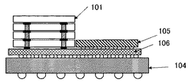
それに対し最近では図1Aに示すような、シリコン貫通ビア(TSV;Through Silicon Via)を使ったチップ積層技術が開発されている。TSVはシリコン基板に設けた貫通電極であり、積層したチップ間及びチップとパッケージ基板間に対して、TSVを用いて電気的に接続することができる。図1AはロジックチップとメモリーチップをTSVにより3次元積層した積層マルチチップパッケージ(3Dパッケージとも呼ばれる)の例である。この例では4枚のメモリチップ101を積層した場合を示している。各メモリーチップ101間及びロジックチップ105とパッケージ基板104の間はTSV102を介して導通されており、バンプ103により接続されている。バンプ103は、はんだまたは銅などの金属で形成される。このようなTSVを使ったチップ積層技術により、従来使用していたワイヤが必要なくなることから積層するチップの枚数を容易に増やすことが可能となり、さらにチップ間及びチップとパッケージ基板間の接続距離が短縮され高速信号の伝達にも有利となる。さらに従来のワイヤボンディング用のワイヤは直径が20〜30μmであったのに対し、TSVは直径10μm以下で形成することが可能であることからより多くの端子を引き出すことが可能となり、大容量通信も可能となるなど多くのメリットがある。
On the other hand, recently, a chip stacking technique using a through silicon via (TSV; Through Silicon Via) as shown in FIG. 1A has been developed. TSV is a through electrode provided on a silicon substrate, and it is possible to electrically connect between the stacked chips and between the chip and the package substrate by using the TSV. FIG. 1A shows an example of a stacked multi-chip package (also called a 3D package) in which a logic chip and a memory chip are three-dimensionally stacked by TSV. In this example, a case where four
しかしTSV付き半導体チップの製造には多くの工程が必要とされ,そのため製造に時間およびコストがかかることが問題となっている。さらにロジックチップにTSVを形成する図1A記載の3Dパッケージの場合、メモリーチップとロジックチップとを同ピッチのTSVで接続するので、ロジックチップ、メモリーチップの各メーカー間でのTSVバンプピッチの統一規格を設ける必要がある。この場合ロジックチップの設計的制約が生じ、設計コストがかかる問題が生じる。さらに3Dパッケージの場合、ロジックチップ、メモリーチップメーカーでそれぞれ製造されたチップを組み立てメーカーで接合し、さらに半導体パッケージ基板に搭載する必要がある。半導体パッケージまで組み立てた後に不具合発生が判明した場合、組み立てメーカーでの不具合か、あるいは何れかのチップメーカーの製造上の不具合かが明確化できないという品質保証や製造責任等の問題も多く、普及の障害になっている。 However, many steps are required to manufacture the semiconductor chip with TSV, which causes a problem that manufacturing takes time and cost. Further, in the case of the 3D package shown in FIG. 1A in which the TSV is formed on the logic chip, since the memory chip and the logic chip are connected with the TSV having the same pitch, a unified standard of the TSV bump pitch between the manufacturers of the logic chip and the memory chip. Need to be provided. In this case, there is a problem in that the design cost of the logic chip is limited and the design cost is increased. Further, in the case of the 3D package, it is necessary to assemble the chips manufactured by the logic chip manufacturer and the memory chip manufacturer by the assembly manufacturer and then mount the chips on the semiconductor package substrate. When defects are discovered after assembling even semiconductor packages, there are many problems such as quality assurance and manufacturing responsibility that it is not possible to clarify whether it is a defect at the assembly manufacturer or a manufacturing defect of any chip manufacturer, which is an obstacle to popularization It has become.
以上のことから、比較的TSV積層が容易なDRAMメモリーの3次元チップと、ロジックチップとを半導体パッケージ基板上で横置きして実装した、図1Bに示すマルチチップパッケージが最も現実的と考えられている(いわゆる2.5Dパッケージ)。3Dパッケージにおいてはメモリーとロジック間の信号配線は、微小なTSVにより接続されるが、2.5Dパッケージの場合、複数の半導体チップ間の信号線接続を半導体パッケージ基板上で平面接続することが必要となる。よって半導体パッケージ基板側には必然的に配線本数が著しく多く必要となることから、微細・多層化の要求が一段と厳しくなってきており、本用途ではL/S=5/5μm以下の微細配線形成技術とビア径30μm以下の層間接続が必要とされる。そこで、2.5Dパッケージでは、図1Bに示すように、3次元積層メモリーとロジックチップとを微細接続可能な、半導体プロセスで製造されたシリコンインターポーザー106上に実装し、さらに半導体チップが搭載されたシリコンインターポーザー106を半導体パッケージ基板104上に実装する方法が提案されている(特許文献1〜4参照)。
From the above, it is considered that the multi-chip package shown in FIG. 1B, in which the three-dimensional chip of the DRAM memory in which TSV stacking is relatively easy and the logic chip are horizontally mounted on the semiconductor package substrate, is most realistic. (So-called 2.5D package). In the 3D package, the signal wiring between the memory and the logic is connected by a minute TSV, but in the 2.5D package, the signal line connection between the plurality of semiconductor chips needs to be planarly connected on the semiconductor package substrate. Becomes Therefore, the number of wirings is inevitably large on the semiconductor package substrate side, and the demand for finer/multi-layered is becoming more severe. In this application, fine wiring with L/S=5/5μm or less is formed. Technology and interlayer connection with a via diameter of 30 μm or less are required. Therefore, in the 2.5D package, as shown in FIG. 1B, the three-dimensional laminated memory and the logic chip are mounted on a
しかしながら、シリコンインターポーザーはウエハープロセスで製造されるので、ウエハよりも大型パネルサイズで製造されている半導体パッケージ基板と比較すると製造コストが高いという問題を生じる。さらにシリコンインターポーザーにおいてはTSV形成のプロセスコストが高いという問題があった。またシリコンは半導体であるため、配線回路を形成するためには、シリコン表面に酸化膜を形成して絶縁化した上に回路配線を形成することが必要である。よってシリコンインターポーザー上に形成された配線回路の伝送特性は、絶縁体であるガラス基板、あるいはガラスエポキシ基板上に形成された回路と比較すると悪くなるという問題があった。 However, since the silicon interposer is manufactured by a wafer process, there is a problem that the manufacturing cost is higher than that of a semiconductor package substrate manufactured in a panel size larger than that of the wafer. Further, the silicon interposer has a problem that the process cost for forming the TSV is high. Further, since silicon is a semiconductor, in order to form a wiring circuit, it is necessary to form an oxide film on the silicon surface to insulate it and then form circuit wiring. Therefore, there is a problem that the transmission characteristics of the wiring circuit formed on the silicon interposer are worse than those of the circuit formed on the glass substrate or the glass epoxy substrate which is an insulator.
そこでシリコン以外の材料をコア層にもつインターポーザーとしてガラスインターポーザーが着目されつつあり研究開発が活発化してきている。コア層にガラスを用いる利点として、種々の厚さやサイズが充実しており限定されないこと、安価であること、平滑性、平坦性に優れることより、L/S=5/5μm以下の微細配線形成性に有利なこと、線熱膨張係数(CTE)がシリコンと同様3ppm前後であり、実装安定性、寸法安定性に優れかつ高弾性であること、化学的安定性に優れること、高い絶縁性と伝送特性などが上げられる。さらにその光学的透明性より撮像素子等の光学素子用途としても着目されつつある。さらにガラス基板への貫通穴形成技術も発展してきており、放電加工やレーザー加工により、ガラス厚300μmであっても直径50μm以上100μm以下の微細な貫通穴加工も可能となってきている。 Therefore, the glass interposer is attracting attention as an interposer having a material other than silicon as the core layer, and research and development have been activated. The advantage of using glass for the core layer is that various thicknesses and sizes are not limited, and it is inexpensive, and smoothness and flatness are excellent. Therefore, fine wiring with L/S=5/5 μm or less is formed. That the linear thermal expansion coefficient (CTE) is around 3 ppm, which is similar to that of silicon, it has excellent mounting stability, dimensional stability, and high elasticity, excellent chemical stability, and high insulation. The transmission characteristics can be improved. Furthermore, due to its optical transparency, it is also gaining attention as a use for optical elements such as image pickup elements. Further, a technique for forming a through hole in a glass substrate has been developed, and it has become possible to perform a fine through hole having a diameter of 50 μm or more and 100 μm or less even if the glass thickness is 300 μm by electric discharge machining or laser machining.
ここでガラスインターポーザーを例として主なガラスを基体とする回路基板の製造方法について簡単に説明する。本例では半導体パッケージ基板と同等にビルトアップ工法によって製造する方法を示す。先ずは基体となるガラス基板を準備する。ガラス基板に放電加工あるいはレーザー加工等公知方法を用いて、貫通穴を形成する。続いてガラス上に無電解めっきあるいはスパッタ法、蒸着法、CVD法等の公知方法によってガラス表面および貫通穴内表面に1μm以下の薄い金属層を形成して導電化処理を行う。 Here, a glass interposer is taken as an example to briefly explain a method of manufacturing a circuit board using glass as a main body. In this example, a method of manufacturing the semiconductor package substrate by a built-up method, which is equivalent to that of the semiconductor package substrate, is shown. First, a glass substrate to be a base is prepared. Through holes are formed in a glass substrate by using a known method such as electric discharge machining or laser machining. Then, a thin metal layer having a thickness of 1 μm or less is formed on the glass surface and the inner surface of the through hole by a known method such as electroless plating or a sputtering method, a vapor deposition method, a CVD method or the like on the glass, and a conductive treatment is performed.
続く工程では複数経路が考えられる。第1の方法においては、薄い金属層全体に通電して電解めっきを行うことで、両面表層およびスルーホール内に金属を充填するいわゆるスルーホールフィリングが考えられる。この方法では、スルーホール直上にビアを形成でき、省スペース化が図れる利点があるが、直径50μmから100μmであるスルーホール内をすべて電解めっきで充填する場合、両表面金属厚は少なくとも25μm〜50μmと厚くなる。この場合、表面金属上にフォトレストパターンをフォトリソグラフィーにより形成した後に、不要な金属層部分をエッチング除去するサブトラクティブ工法によって配線形成するが、本方法では厚い金属層に対してインターポーザーで要求される微細回路を形成することが不可能となってしまう。さらに、ガラス厚みと穴径のアスペクト比等貫通穴形状にもよるが、スルーホール内を完全に電解めっき層で充填することは困難で、特にアスペクト比が2以上となる場合、スルーホール内にボイドやシームを内包してしまい信頼性が低下する問題があった。 Multiple paths are possible in subsequent steps. In the first method, so-called through-hole filling is conceivable in which electric current is applied to the entire thin metal layer for electrolytic plating to fill the metal in the double-sided surface layer and the through-hole. This method has an advantage that a via can be formed right above the through hole and space can be saved. However, when the inside of the through hole having a diameter of 50 μm to 100 μm is entirely filled with electrolytic plating, both surface metal thicknesses are at least 25 μm to 50 μm. And get thicker. In this case, after forming a photo rest pattern on the surface metal by photolithography, wiring is formed by a subtractive method in which an unnecessary metal layer portion is removed by etching.In this method, a thick metal layer is required by an interposer. It becomes impossible to form a fine circuit. Further, it is difficult to completely fill the inside of the through hole with the electrolytic plating layer, depending on the shape of the through hole such as the glass thickness and the aspect ratio of the hole diameter. Especially, when the aspect ratio is 2 or more, the inside of the through hole is There was a problem that the voids and seams were included and the reliability decreased.
第2の方法では、同様に薄い金属層全体に通電して電解めっきを行うことで、表層両面およびスルーホール内をめっきするが、スルーホールが充填される前にめっきを完了した後に、表面金属上にフォトレストをパターニングして不要な金属層をエッチング除去することで回路形成する方法である。本発明者が検討した結果、本方法においても、L/S=20/20μm程度で微細化限界となり、インターポーザー用途で要求される微細回路を形成することが不可能であった。プリント配線板の公知製造方法である穴埋め印刷、研磨、蓋めっき、サブトラクティブ法による配線形成でも同様にL/S=5/5μm以下の微細配線形成は困難を極めていた。 In the second method, the thin metal layer is similarly energized to carry out electrolytic plating to plate both surfaces of the surface layer and the inside of the through hole, but after the plating is completed before the through hole is filled, the surface metal is In this method, a circuit is formed by patterning a photorest on the top and removing an unnecessary metal layer by etching. As a result of examination by the present inventors, even in this method, it was impossible to form a fine circuit required for an interposer application because the miniaturization limit was reached at L/S=20/20 μm. Similarly, it is very difficult to form fine wiring with L/S=5/5 μm or less even in wiring formation by hole filling printing, polishing, lid plating, and subtractive methods, which are known manufacturing methods for printed wiring boards.
第3の方法は、薄い金属層上にレジスト層を形成し、スルーホール部と配線部上のレジストを除去するようにパターニングした後に、電解めっきによって配線とスルーホールを同時に形成・増膜し、レジスト剥離後に薄い金属層をエッチング除去するセミアディティブ工法によって形成する方法である。本方法によれば、インターポーザーに要求されるL/S=5/5μm以下の微細配線形成が可能となる。さらに後の工程で表層回路上両面にビルトアップ樹脂を真空ラミネーターにて加熱・加圧形成することで表層絶縁層形成と、中空のスルーホール内へのビルトアップ樹脂充填保護を同時に行うことが出来るため効率がよい方法である。 The third method is to form a resist layer on a thin metal layer, perform patterning so as to remove the resist on the through hole portion and the wiring portion, and then simultaneously form and increase the wiring and the through hole by electrolytic plating. In this method, a thin metal layer is removed by etching after the resist is removed by a semi-additive method. According to this method, it is possible to form fine wiring of L/S=5/5 μm or less required for the interposer. In a later process, the build-up resin can be formed on both surfaces of the surface layer circuit by heating and pressurizing it with a vacuum laminator, and the surface layer insulating layer can be formed and the build-up resin filling protection inside the hollow through-hole can be performed at the same time. Therefore, it is an efficient method.
しかしながら上述の第3の方法を行う場合、使用する樹脂によっては真空ラミネート法による充填であっても、スルーホール内部までビルドアップ樹脂を充填ですることができずにエアボイドを内包してしまう結果、半導体装置組み立て工程たとえばマスリフロー等の熱履歴によって、内包したボイドが破裂することによって、回路基板の信頼性を確保できないという問題が生じていた。 However, when the above-mentioned third method is carried out, even if the filling is performed by the vacuum laminating method depending on the resin used, the build-up resin cannot be filled up to the inside of the through hole and the air void is included. A semiconductor device assembling process, for example, a thermal history such as mass reflow, causes the enclosed voids to burst, causing a problem that the reliability of the circuit board cannot be ensured.
さらに流動性が悪い樹脂の場合、スルーホール周辺の樹脂厚が薄くなり、スルーホール直上で凹みを生じることが問題となっていた。流動性が良好な樹脂であって、平坦にラミネートできた場合であっても、スルーホール部分上はスルーホールの無いガラス平面部上と比較して樹脂厚が厚くなるため、樹脂の硬化収縮が大きい場合、スルーホール直上で凹みを生じる不具合を生じていた。以上よりスルーホール直上の樹脂は5μm程度の凹みを生じてしまい、平坦性が確保できないため微細回路が形成できないという慢性的な問題が生じていた。 Further, in the case of a resin having poor fluidity, the thickness of the resin around the through hole becomes thin, which causes a problem that a recess is formed directly above the through hole. Even if the resin has good fluidity and can be laminated flat, the resin thickness on the through-hole part is thicker than on the flat glass part without the through-hole, so that the curing shrinkage of the resin does not occur. In the case of a large size, there was a problem that a recess was formed immediately above the through hole. As described above, the resin immediately above the through hole has a recess of about 5 μm, and since the flatness cannot be secured, a chronic problem that a fine circuit cannot be formed occurs.
さらにガラス回路直上に形成する樹脂の線熱膨張係数が大きい場合、後の工程での熱履歴が加わることによってガラス基板と絶縁樹脂層との線熱膨張係数の違いに起因する応力が蓄積するために、ガラスコア基板を個片化するダイシング工程において、ガラス厚み内で平面方向へ剥離するように破断する背ワレ現象が起こりやすくなるという問題を生じていた。 Furthermore, when the linear thermal expansion coefficient of the resin formed directly above the glass circuit is large, the stress due to the difference in the linear thermal expansion coefficient between the glass substrate and the insulating resin layer accumulates due to the thermal history in the subsequent process. In addition, in the dicing step of dividing the glass core substrate into pieces, there is a problem that a back crack phenomenon in which the glass core substrate breaks so as to peel off in the plane direction within the glass thickness is likely to occur.
本発明は、上述した課題を解決するためになされたものであり、その目的とするところは、長期信頼性を確保しつつ絶縁樹脂層の平坦性を確保することによって微細回路形成可能にし、さらに微細多層回路形成が容易なガラスを基体とする配線基板およびその製造方法を提供することにある。 The present invention has been made in order to solve the above-mentioned problems, and an object thereof is to make it possible to form a fine circuit by ensuring the flatness of an insulating resin layer while ensuring long-term reliability. It is an object of the present invention to provide a glass-based wiring board on which a fine multilayer circuit can be easily formed and a method for manufacturing the same.
本発明の一局面は、ガラス基板両面を貫通形成する貫通穴と、少なくとも貫通穴内壁を被覆する円筒状中空の金属層よりなるスルーホールと、ガラス基板両面に形成された金属回路とを有するガラス回路基板であって、両面に形成された金属回路の一部はスルーホールと接続され、表裏が電気的に導通され、少なくともスルーホール中空部とガラス回路基板両面とが同一の第一絶縁樹脂で充填被覆され、第一絶縁樹脂は、熱硬化性樹脂、無機フィラーを含み、無機フィラーの平均粒径0.4μm以上、最大粒径5μm以下、無機フィラー充填量が60wt%以上、25℃からガラス転移温度以下までの平均線熱膨張係数が25ppm以下であり、第一絶縁樹脂上にビアホールおよび金属回路が形成され、第一絶縁樹脂に1以上の第二絶縁樹脂の層が積層され、第二絶縁樹脂の各層上にビアホールおよび金属回路が形成されており、第二絶縁樹脂は、熱硬化性樹脂、無機フィラーを含み、無機フィラーの平均フィラー径が0.2μm以下、最大フィラー径が2μm以下、無機フィラー充填量が65wt%以下である。 One aspect of the present invention is a glass having a through hole formed through both surfaces of a glass substrate, a through hole formed of a cylindrical hollow metal layer covering at least the inner wall of the through hole, and a metal circuit formed on both surfaces of the glass substrate. In the circuit board, a part of the metal circuit formed on both sides is connected to the through hole, the front and back sides are electrically conducted, and at least the hollow part of the through hole and both surfaces of the glass circuit board are made of the same first insulating resin. Filled and coated, the first insulating resin contains a thermosetting resin and an inorganic filler, the inorganic filler has an average particle size of 0.4 μm or more, a maximum particle size of 5 μm or less, an inorganic filler filling amount of 60 wt% or more, and glass from 25° C. the average linear thermal expansion coefficient of up to below the transition temperature of Ri der less 25 ppm, via holes and metal circuit on the first insulating resin is formed, a layer of one or more second insulating resin on the first insulating resin is laminated, the A via hole and a metal circuit are formed on each layer of the second insulating resin, and the second insulating resin contains a thermosetting resin and an inorganic filler, and the average filler diameter of the inorganic filler is 0.2 μm or less and the maximum filler diameter is 2 μm. hereinafter, the inorganic filler loading is Ru der less 65 wt%.
また、金属層と、ガラス基板両面、第一絶縁樹脂、および、第二絶縁樹脂の各層に形成された金属回路とが、少なくとも銅、ニッケル、チタン、クロムのいずれかを含んでもよい。 Further, a metal layer, a glass substrate duplex, the first insulating resin, and a metal circuit formed on each layer of the second insulating resin is at least copper, nickel, titanium, may include either chromium.
本発明によれば、貫通スルーホールおよびガラス両面に金属回路が形成されているガラスコア基板に、スルーホール内部への充填性がよい第1絶縁樹脂をガラスコア基板両面にラミネートすることによって、スルーホール内に発生するボイドを効果的に抑制することが出来るので、長期接続信頼性を有するガラスコア基板を提供することが出来る。さらに本発明によれば、第1絶縁樹脂は無機フィラーの充填量が多いので、スルーホール内部に充填される絶縁樹脂の硬化収縮量を抑制することが可能となり、スルーホール直上における硬化収縮に起因する凹みを抑制することで樹脂表面の平坦性を確保することができる。よって、微細回路形成が容易なガラス回路基板およびその製造方法を提供できる。さらに第1絶縁樹脂上にはさらに微細配線、小径ビア加工が容易な第2の絶縁樹脂を用いることによって微細多層配線層を有するガラス回路基板を提供できる。 According to the present invention, a glass core substrate having through-holes and metal circuits formed on both sides of the glass is laminated with a first insulating resin having good filling properties into the through holes on both sides of the glass core substrate. Since voids generated in the holes can be effectively suppressed, it is possible to provide a glass core substrate having long-term connection reliability. Furthermore, according to the present invention, since the first insulating resin has a large amount of the inorganic filler filled therein, it is possible to suppress the amount of curing shrinkage of the insulating resin filled inside the through hole, which results from the curing shrinkage just above the through hole. The flatness of the resin surface can be ensured by suppressing the depression. Therefore, it is possible to provide a glass circuit board on which a fine circuit can be easily formed and a manufacturing method thereof. Further, a glass circuit board having a fine multi-layer wiring layer can be provided by using a second insulating resin on which the fine wiring and small-diameter vias can be easily processed on the first insulating resin.
以下本発明の一実施形態について、断面図である図面2A〜2Mを参照して詳細説明する。本実施形態は本発明の実施形態の一例であって、以下の説明によって本発明のガラスコア基板を限定するものではない。 An embodiment of the present invention will be described below in detail with reference to the sectional views 2A to 2M. This embodiment is an example of the embodiment of the present invention, and the glass core substrate of the present invention is not limited by the following description.
先ずは図2A記載の貫通穴202が形成されたガラスコア201を準備する。ガラスコア201はガラス材料に対して公知方法で貫通穴202を設けて形成出来る。ガラス材料は、本発明を限定するものではないが、SiO2を主成分とする。ガラス材料は、3〜4ppm/℃の線膨張率を有する低膨張ガラス、8〜9ppm/℃の線膨張率を有するソーダガラスなどを用いることができる。ガラス材料の線膨張率は、製造方法の変更、またはNaなどの金属成分の添加により3〜9ppm/℃の範囲内で調整することができる。線膨張係数(CTE)は、ガラスに関するJIS R3102:1995またはプラスチックに関するJIS K7197:2012にしたがって、熱機械分析(TMA)により測定することができる。ガラス基板は50μm〜1000μmの範囲の厚さを有することが望ましい。より望ましくは100μm以上、500μm以下が望ましい。50μm以下である場合、製造工程中において取り扱いが困難となる。1000μm以上である場合、直径100μm以下、ピッチ200μm以下の微細な貫通穴加工が困難となる。
First, a
貫通穴加工として公知方法としては、レーザー加工、放電加工、感光性レジスト材料を用いる場合ではサンドブラスト加工、ドライエッチング、フッ化水素酸等によるケミカルエッチング加工が挙げられる。さらに感光性ガラスを用いてもガラスコアを作成することが可能である。好ましくはレーザー加工、放電加工が簡便でスループットが良いことから望ましい。用いることができるレーザーは、CO2レーザー、UVレーザー、ピコ秒レーザー、フェムト秒レーザーなどから選択することができる。 Known methods for the through-hole processing include laser processing, electric discharge processing, sandblasting when a photosensitive resist material is used, dry etching, and chemical etching processing using hydrofluoric acid or the like. Further, the glass core can be prepared by using a photosensitive glass. Laser processing and electric discharge processing are preferable because they are simple and have high throughput. A laser that can be used can be selected from a CO 2 laser, a UV laser, a picosecond laser, a femtosecond laser, and the like.
続いて、図2Bに記載するように、ガラスコア基板201のスルーホール内壁および表面に導電層203を形成する。導電層203の形成は、ガラスコア基板201上に密着層(不図示)の導入後に実施してもよい。密着層とは、ガラス表面と導電層203との密着性を改善するために導入されるもので、本発明を限定するものではないが、一例としては酸化スズ、酸化インジウム、酸化亜鉛、ニッケル−リン(Ni−P)、クロム、酸化クロム、窒化アルミニウム、窒化銅、酸化アルミニウム、タンタル、チタンおよび銅からなる群から選択される1つまたは複数から選択することができる。より好ましくはチタン、クロムより選択されることが望ましい。密着層の厚みは本発明を限定するものではないが、0.01μm以上1μm以下であることが望ましい。密着層は、たとえば、スパッタ法、無電解めっき法、CVD法、蒸着法などの当該技術において知られている任意の技術を用いて形成することができる。
Subsequently, as shown in FIG. 2B, the
導電層203は電気的に接続安定性の高い材料であることが望ましい。用いることができる材料は、たとえば、銅、銀、金、ニッケル、白金、パラジウム、ルテニウムおよびスズからなる群から選択される金属、およびスズ−銀、スズ−銀−銅、スズ−銅、スズ−ビスマス、およびスズ−鉛からなる群から選択される合金を含む。好ましくは銅あるいはニッケルであることが望ましい。導電層の厚みは本発明を限定するものではないが、0.01μm以上1μm以下であることが望ましい。導電層の形成法は、たとえば、スパッタ法、無電解めっき法、CVD法、蒸着法等より選択することが出来る。
The
続いて、図2Cに記載するように導電層203が形成されているガラスコア基板上にレジストパターン204を形成する。レジストは液状ポジレジスト、液状ネガレジスト、ドライフィルムレジストより選択することができる。液状レジストの塗布方法であれば、スリットコート、カーテンコート、ダイコート、スプレーコート、静電塗装、インクジェットコート、グラビアコート、スクリーン印刷、グラビアオフセット印刷、スピンコート、ドクターコートより選定できる。ドライフィルムレジストであれば、ロールラミネーターによりレジスト層を形成することができる。導電層両表面にレジスト層を形成した後に、所望のパターンをフォトリソグラフィー法によってガラスコア基板上に形成する。レジストパターンは後の電解めっき層が形成される部分が露出するように位置あわせの上パターニングする。レジスト層の厚みであるが、後工程の電解めっき厚にも依存するが、好ましくは3μm以上、25μm以下であることがのぞましい。3μmより薄い場合電解めっきを3μm以上に増膜できなくなり、回路の接続信頼性が低下する可能性がある。25μmより厚くなる場合、L/S=5/5μm以下の微細配線を形成することが困難となる。
Subsequently, as shown in FIG. 2C, a resist
続いて図2Dに記載するように、導電層を利用して電解めっきによって電解めっき回路層205を形成する。電解めっきによってスルーホール内壁206および回路部分の金属層を増膜することができる。電解めっきを行うことができる金属としては、銅、ニッケル、錫、金、銀、はんだ等より選択することが出来る。望ましくは銅、ニッケルであることが簡便かつ安価であるため望ましい。電解めっきの厚さであるが、1μm以上、20μm以下であることが望ましい。電解めっき層が1μm以下である場合、回路の接続信頼性を維持できない可能性がある。20μmより厚い場合、厚み20μm以上のレジストパターンを形成することが困難であるので微細回路を形成することができない。
Subsequently, as shown in FIG. 2D, an electrolytic plated
続いて図2D記載の電解めっき後に不要となったフォトレジスト204を剥離後に、導電層203をエッチング除去することで回路として分離することで、図2Eに記載するように両面に回路層205が形成されたガラスコア基板が得られる。
Subsequently, after removing the
図2Fに記載するように、ガラスコア基板両面に第一絶縁樹脂層207を形成し、スルーホール部の穴埋めも行う。第一絶縁樹脂層の厚みはガラスコア基板両面に形成された回路層205上面より5μm以上30μm以下の厚みになるように調整する。5μm未満となる場合、層間の絶縁性を確保することが困難となる。30μmより大きい場合、30μm以下の微小なビアホールを形成することが困難となる。絶縁樹脂の形成方法は本発明では限定されないが、支持体フィルム上に形成された第一絶縁樹脂層を真空ラミネーターで熱圧着して形成する方法が一般的かつ簡便で生産性が良いため望ましい。ラミネート後に熱硬化させることによって第一絶縁樹脂層を形成することが出来る。支持体フィルムの剥離は熱硬化前あるいは熱硬化後であっても良く適宜行う。
As shown in FIG. 2F, the first insulating
本発明における第一絶縁樹脂は、熱硬化性樹脂、無機フィラーから構成されている。熱硬化性樹脂としては、エポキシ樹脂、フェノール樹脂、尿素樹脂、メラミン樹脂、不飽和ポリエステル樹脂、ポリイミド樹脂、シアネート樹脂、ポリイミド樹脂、ベンゾシクロブテン樹脂、ポリベンゾオキサゾール樹脂、シクロオレフィン樹脂およびこれらの変性物が挙げられる。これら樹脂は単独であっても組み合わせで用いてもよい。より好ましくはエポキシ樹脂、シアネート樹脂が一般的であることから望ましい。 The first insulating resin in the present invention is composed of a thermosetting resin and an inorganic filler. Examples of the thermosetting resin include epoxy resin, phenol resin, urea resin, melamine resin, unsaturated polyester resin, polyimide resin, cyanate resin, polyimide resin, benzocyclobutene resin, polybenzoxazole resin, cycloolefin resin and modifications thereof. Things can be mentioned. These resins may be used alone or in combination. Epoxy resin and cyanate resin are more preferable because they are common.
本発明における第一絶縁樹脂の無機フィラーは、ガラス、シリカ、アルミナ等の酸化物、水酸化カルシウムのような水酸化物、炭酸カルシウムのような炭酸塩、硫酸バリウムのような硫酸塩、タルク、マイカ、ワラストナイト等珪酸塩などが挙げられるが、好ましくは球状シリカであることが望ましい。その理由として粒径のそろった球状のものが得られやすいために粒径制御が容易なこと、シランカップリング処理などの表面処理が可能であるためである。 The inorganic filler of the first insulating resin in the present invention, glass, silica, oxides such as alumina, hydroxides such as calcium hydroxide, carbonates such as calcium carbonate, sulfates such as barium sulfate, talc, Examples thereof include silicates such as mica and wollastonite, and spherical silica is preferable. The reason is that spherical particles having a uniform particle size are easily obtained, so that the particle size can be easily controlled and surface treatment such as silane coupling treatment is possible.
第一絶縁樹脂は、無機フィラーの平均粒径0.4μm以上、最大フィラー径5μm以下、無機フィラー充填量が60wt%以上であることが好ましい。無機フィラーの平均粒径はレーザー回折粒度分布測定装置(日機装株式会社製マイクロトラック MT 3300EX)によって測定された値である。本発明者が研究を重ねた結果、スルーホール内への樹脂充填・埋め込み性、硬化収縮、30μm以下の小径ビア加工性は無機フィラー径および分布、無機フィラーの充填量によるところが大きいことが判明し本発明に至った。無機フィラーの平均粒径は樹脂充填性および小径ビア加工性、フィラー充填量に影響する。0.4μm未満になる場合、真空熱ラミネート時に粘度が十分に下がりきらないために流動性が確保できず、スルーホール内部へのエアボイドが発生する確率が高くなることがわかった。さらに本発明による最大粒径は5μm以下である。最大粒径が5μmより大きい場合、30μm以下の微細なビアホールを加工する場合に形状が悪く、所定の大きさで加工することが困難となるために最大フィラー径は5μm以下である必要がある。フィラー充填量を大きくする場合、単一粒子径の無機フィラーでは細密充填困難であるため実現不可能である。よって平均粒径が0.4μm以上、最大粒子径が5μm以下の粒度分布が好適である。 The first insulating resin preferably has an average particle diameter of the inorganic filler of 0.4 μm or more, a maximum filler diameter of 5 μm or less, and an inorganic filler filling amount of 60 wt% or more. The average particle size of the inorganic filler is a value measured by a laser diffraction particle size distribution measuring device (Microtrac MT 3300EX manufactured by Nikkiso Co., Ltd.). As a result of repeated studies by the present inventor, it was found that the resin filling/embedding property in the through hole, the curing shrinkage, and the workability of small-diameter vias of 30 μm or less largely depend on the inorganic filler diameter and distribution and the inorganic filler filling amount. The present invention was reached. The average particle size of the inorganic filler affects the resin filling property, the small diameter via processing property, and the filler filling amount. It was found that when the thickness is less than 0.4 μm, the fluidity cannot be ensured because the viscosity does not fall sufficiently during vacuum heat lamination, and the probability of air voids occurring inside the through hole increases. Further, the maximum particle size according to the present invention is 5 μm or less. If the maximum particle size is larger than 5 μm, the shape is not good when processing a fine via hole of 30 μm or less, and it becomes difficult to process with a predetermined size, so the maximum filler diameter needs to be 5 μm or less. In the case of increasing the filler filling amount, it is difficult to achieve fine packing with an inorganic filler having a single particle size, which is impossible. Therefore, a particle size distribution having an average particle size of 0.4 μm or more and a maximum particle size of 5 μm or less is suitable.
また、樹脂の硬化収縮量は無機フィラー充填量で効果的に制御できることが判明し発明に至った。本発明による第一絶縁樹脂の無機フィラー充填量は60wt%以上である。60Wt%未満である場合硬化収縮による影響が大きく、スルーホール直上部208は硬化収縮による凹みが5μmを超える部分が発生してしまう。絶縁樹脂表面にL/S=5/5μm以下の微細配線を歩留まり良く製造できなくなる。さらにフィラー充填量が60wt%未満となる場合、第一絶縁樹脂層の線熱膨張係数(CTE)が十分低減できなくなる。本発明による第一絶縁樹脂は、25℃からガラス転移温度以下の線熱膨張係数(CTE)が25ppm以下となるように調整する。線熱膨張係数を25ppm以下に調整とすることで、回路を個片化するときに、ガラス厚み内平面方向へ剥離するように破断する背ワレ不良を抑制することが可能となる。線熱膨張係数は、プラスチックに関するJIS K7197:2012にしたがって、熱機械分析(TMA)により測定することができる。
Further, it was found that the curing shrinkage amount of the resin can be effectively controlled by the inorganic filler filling amount, and the present invention was accomplished. The inorganic filler filling amount of the first insulating resin according to the present invention is 60 wt% or more. When it is less than 60 Wt %, the curing shrinkage has a large effect, and the
続いて図2Gに記載するように、公知方法でビアホール209を形成する。ここで形成するビアホール径は50μm以下であることが望ましい。より好ましくは30μm以下であることが高密度配線を形成できるため望ましい。ビアホール形成はレーザー加工機であることが望ましい。レーザー加工機はCO2レーザー、UVレーザー、ピコ秒レーザー、フェムト秒レーザーなどから選択することができる。より好ましくはUVレーザーであることがビアホールの小径加工に有利であることから望ましい。公知のレーザー加工によりビアホール形成後、レーザー加工後のスミアを公知のデスミア処理を行うことで除去することが望ましい。
Subsequently, as shown in FIG. 2G, a via
続いて図2H記載のように第一絶縁樹脂およびビアホール内部への導電層203を形成する。導電層は無電解めっき、スパッタ、CVD法、蒸着法から選択される方法によって形成することが出来る。たとえば無電解めっきであれば無電解銅めっき、無電解ニッケルめっきより選択することが出来る。好ましくは無電解銅めっきであることが望ましい。スパッタ、CVDあるいは蒸着法であれば、銅、銀、金、チタン、ニッケル、白金、パラジウム、クロム等より選択することが出来る。これらは組み合わせて用いても良いし単独で用いても良い。より好ましくは銅、ニッケル、チタン、クロムであることが樹脂との密着性が良いことから望ましい。導電層の総厚は2μm以下であることが望ましい。より好ましくは1μm以下であることが、微細配線形成に有利なことから望ましい。
Subsequently, as shown in FIG. 2H, the first insulating resin and the
図2Iの工程は先の図2Cの工程と同様に導電層203上にレジストパターン204を形成する工程である。レジストは先と同様に液状ポジレジスト、液状ネガレジスト、ドライフィルムレジストより選択することができる。レジスト層の形成方法であるが、先に説明した方法と同方法を用いることが出来る。導電層両表面にレジスト層を形成した後に、フォトリソグラフィー法によりパターン形成する。レジスト層の厚みは先と同様3μm以上、25μm以下であることがのぞましい。3μmより薄い場合電解めっきを3μm以上に増膜できなくなり、回路の接続信頼性が低下する可能性がある。25μmより厚くなる場合、L/S=5/5μm以下の微細配線を形成することが困難となる。
The step of FIG. 2I is a step of forming the resist
続いて図2Jに記載する断面図は、先の説明と同様に図2Iの導電層203上にレジストパターン204を形成した後に、電解めっきを行い、レジスト層を剥離除去した後に導電層203をエッチング除去した基板の模式図である。本発明における第一絶縁樹脂では、スルーホール直上部208であっても5μm以上の凹みを生じることがないため、L/S=5/5μm以下の微細配線であっても歩留まり良く製造することが可能となる。
Subsequently, in the cross-sectional view illustrated in FIG. 2J, similarly to the above description, after forming the resist
本発明によれば図2Kに記載するように、第一絶縁樹脂層207上に形成された回路層205上に第二絶縁樹脂層210を形成する。第二絶縁樹脂層の厚さは回路層205上面より5μm以上30μm以下の厚みになるように調整する。5μm以下となる場合、層間の絶縁性を確保することが困難となる。30μm以上となる場合、30μm以下の微小なビアホールを形成することが困難となる。絶縁樹脂の形成方法は本発明では限定されないが、支持体フィルム上に形成された第一絶縁樹脂層を真空ラミネーターで熱圧着して形成する方法が一般的かつ簡便で生産性が良いため望ましい。ラミネート後に熱硬化させることによって第一絶縁樹脂層を形成することが出来る。支持体フィルムの剥離は熱硬化前あるいは熱硬化後であっても良く適宜行う。
According to the present invention, as shown in FIG. 2K, the second insulating
本発明における第二絶縁樹脂は、熱硬化性樹脂、無機フィラーから構成されている。熱硬化性樹脂としては、エポキシ樹脂、フェノール樹脂、尿素樹脂、メラミン樹脂、不飽和ポリエステル樹脂、ポリイミド樹脂、シアネート樹脂、ポリイミド樹脂、ベンゾシクロブテン樹脂、ポリベンゾオキサゾール樹脂、シクロオレフィン樹脂およびこれらの変性物が挙げられる。これら樹脂は単独であっても組み合わせで用いてもよい。より好ましくはエポキシ樹脂、シアネート樹脂が一般的であることから望ましい。 The second insulating resin in the present invention is composed of a thermosetting resin and an inorganic filler. Examples of the thermosetting resin include epoxy resin, phenol resin, urea resin, melamine resin, unsaturated polyester resin, polyimide resin, cyanate resin, polyimide resin, benzocyclobutene resin, polybenzoxazole resin, cycloolefin resin and modifications thereof. Things can be mentioned. These resins may be used alone or in combination. Epoxy resin and cyanate resin are more preferable because they are common.
本発明における第二絶縁樹脂の無機フィラーは、ガラス、シリカ、アルミナ等の酸化物、水酸化カルシウムのような水酸化物、炭酸カルシウムのような炭酸塩、硫酸バリウムのような硫酸塩、タルク、マイカ、ワラストナイト等珪酸塩などが挙げられるが、好ましくは球状シリカであることが望ましい。その理由として粒径のそろった球状のものが得られやすいために粒径制御が容易なこと、シランカップリング処理などの表面処理が可能であるためである。 The inorganic filler of the second insulating resin in the present invention, glass, silica, oxides such as alumina, hydroxides such as calcium hydroxide, carbonates such as calcium carbonate, sulfates such as barium sulfate, talc, Examples thereof include silicates such as mica and wollastonite, and spherical silica is preferable. The reason is that spherical particles having a uniform particle size are easily obtained, so that the particle size can be easily controlled and surface treatment such as silane coupling treatment is possible.
第二絶縁樹脂は、平均フィラー径が0.2μm以下、最大フィラー径が2μm以下、無機フィラー充填量が65wt%以下であることが好ましい。本発明者が研究を重ねた結果、第一絶縁樹脂層ではスルーホール内部への充填性特性が重要だが第二絶縁樹脂層では不要であり、微小ビア形成性、微細配線形成性に特化してより高密度な配線形成を可能にすることを目的に検討を加えた。その結果、L/S=5/5μm以下、さらに好ましくはL/S=3/3μm以下の微細配線形成性、ビア径30μm以下、さらに好ましくは20μm以下の小径ビアホールの形成においては、平均フィラー径が0.2μm以下、最大フィラー径が2μm以下であると微細回路の形成性が良好であることを見出し本発明に至った。平均フィラー径が0.2μmより大きい場合、20μm以下のビア加工形状が悪化する結果となる。さらに0.2μmより大きい場合、スミア後の樹脂表面の凹凸が大きくL/S=3/3μm以下の微細配線形成が歩留まり良く製造できない結果となる。最大フィラー径が2μmより大きい場合、微細配線間のスペース部分への樹脂充填性が悪化し、膨れの原因となる。本発明による無機フィラーの平均粒径はレーザー回折粒度分布測定装置によって測定された値である。 The second insulating resin preferably has an average filler diameter of 0.2 μm or less, a maximum filler diameter of 2 μm or less, and an inorganic filler filling amount of 65 wt% or less. As a result of repeated studies by the present inventor, the filling property inside the through hole is important in the first insulating resin layer, but not necessary in the second insulating resin layer, and it is specialized in fine via forming property and fine wiring forming property. A study was conducted for the purpose of enabling higher density wiring formation. As a result, L/S=5/5 μm or less, more preferably L/S=3/3 μm or less fine wiring formability, and a via diameter of 30 μm or less, more preferably 20 μm or less. Of 0.2 μm or less and a maximum filler diameter of 2 μm or less, the present invention was found to have good formability of fine circuits. When the average filler diameter is larger than 0.2 μm, the via processed shape of 20 μm or less is deteriorated. Further, if it is larger than 0.2 μm, the unevenness of the resin surface after smear is large, and the result is that the fine wiring with L/S=3/3 μm or less cannot be manufactured with a high yield. When the maximum filler diameter is larger than 2 μm, the resin filling property into the space between the fine wirings deteriorates, which causes swelling. The average particle size of the inorganic filler according to the present invention is a value measured by a laser diffraction particle size distribution measuring device.
さらにフィラー充填量が65wt%より大きい場合、レーザービア加工後のデスミア処理において、樹脂表面にフィラーが露出してしまい、後工程における導電層との密着性が悪化するために配線のハガレを生じてしまい、細線形成性が悪くなることが判明した。よってフィラー充填量は65wt%以下であることが望ましい。以上より、平均フィラー径が0.2μm以下、最大フィラー径が2μm以下、無機フィラー充填量が65wt%以下であることが第二絶縁樹脂として好適である。 Further, when the filler filling amount is larger than 65 wt %, the filler is exposed on the resin surface in the desmear treatment after the laser via processing, and the adhesiveness with the conductive layer in the subsequent step is deteriorated, causing peeling of the wiring. It was found that the fine line formability deteriorates. Therefore, the filler filling amount is preferably 65 wt% or less. From the above, it is suitable for the second insulating resin that the average filler diameter is 0.2 μm or less, the maximum filler diameter is 2 μm or less, and the inorganic filler filling amount is 65 wt% or less.
図2K記載の第二絶縁樹脂層210形成以降の工程は、先に説明した図2G〜2Jと同工程を繰り返すことで第二絶縁樹脂層210上に配線層205を形成することが出来る(図2L)。第二絶縁樹脂層210、第二絶縁樹脂層上の回路層厚は、第一絶縁樹脂層207および第一絶縁樹脂層上の回路層と同等であっても良いがより好ましくは薄くしても良い。ビアホール径も第一絶縁樹脂層と同等であっても良いがより好ましくは小径にしても良い。図2Mに第二絶縁樹脂層210形成と配線層形成をさらに2回繰り返すことで、ガラスを基体とする多層回路基板を作成した模式図を記載する。
In the steps after the formation of the second insulating
(ガラスコア基板の作成)
本発明の実施例および比較例として、図2A〜2Mに示す工程によって、4−2−4構造のガラス回路基板を製造した。厚さ0.3mmのガラス基板に、公知技術であるCO2レーザーにて穴径100μmの貫通スルーホールを形成し、500℃でアニールすることによって加工歪を除去した(図2A)。続いて、図2B記載のようにチタン層0.05μm、銅層0.5μmをスパッタ処理することで、導電層203を形成した。続いて、10μm厚のドライフィルムレジストを両面形成後、最小線幅L/S=5/5μmが描画されたフォトマスクを用いて両面パターニング後、1%炭酸ソーダで現像処理することによって、パターニングされたガラス基板を得た(図2C)。さらに電解めっきを7μm厚で行い(図2D)、レジスト剥離後に硫酸−過酸化水素よりなるエッチング液にて導電層の銅層、水酸化カリウム−過酸化水素混合エッチャントでチタン層を除去することで、ガラス上に回路が形成された基板(図2E)を得た。
(Creation of glass core substrate)
As an example and a comparative example of the present invention, a glass circuit board having a 4-2-4 structure was manufactured by the steps shown in FIGS. A through-hole having a hole diameter of 100 μm was formed on a glass substrate having a thickness of 0.3 mm by a known technique of CO 2 laser, and annealing was performed at 500° C. to remove processing strain (FIG. 2A). Subsequently, as shown in FIG. 2B, the titanium layer 0.05 μm and the copper layer 0.5 μm were sputtered to form the
(第一絶縁樹脂層形成と回路形成)
続いて厚さ12μmの第一絶縁樹脂として、表1記載の実施例1〜2、比較例1〜3の内容の樹脂を真空ラミネートすることで第一絶縁樹脂層207を形成した(図2F)。第一絶縁樹脂の回路層205上の厚みは10μmであった。続いてUV−YAGレーザーにてビア径25μmのビアホールを形成し、アルカリ性熱過マンガン酸溶液にてデスミア処理を行った(図2G)。デスミア処理後チタン層0.04μm、銅層0.3μmで導電層203をスパッタ法にて両面形成した(図2H)。さらに両面に7μm厚のドライフィルムレジストを形成しパターニングすることで両面に最小線幅L/S=3/3μmのレジストパターンが形成された基板を得た(図2I)。電解めっきを5μm厚で行いレジスト剥離、チタン、銅層をエッチング除去することで第一絶縁樹脂上に回路が形成されたガラス基板を得た(図2J)。
(First insulating resin layer formation and circuit formation)
Subsequently, as the first insulating resin having a thickness of 12 μm, the first insulating
(第二絶縁樹脂層形成と回路形成の繰り返しによる多層回路形成)
続いて厚さ10μmの第二絶縁樹脂として、表1記載の実施例1〜2、比較例1〜3の第二樹脂を真空ラミネートすることで第二絶縁樹脂層210を形成した。第二絶縁樹脂の回路層205上の厚みは7μmであった。以降の工程は図2G〜2Jと同様に行う。続いてUV−YAGレーザーにてビア径15μmのビアホールを形成し、アルカリ性熱過マンガン酸溶液にてデスミア処理を行った。デスミア処理後チタン層0.04μm、銅層0.2μmで導電層をスパッタ法にて両面形成した。さらに両面に5μmで液状ポジレジストを形成しパターニングすることで両面にレジストパターンが形成された基板を得た。電解めっきを4μm厚で行いレジスト剥離、チタン、銅層をエッチング除去することで第2絶縁樹脂上に最小線幅L/S=2/2μmの回路が形成されたガラス多層回路基板を得た(図2L)。さらに第二絶縁樹脂層形成と回路形成を同方法にて繰り返すことによって4−2−4構造のガラスを基体とする多層回路基板が得られた(図2M)。
(Multilayer circuit formation by repeating second insulating resin layer formation and circuit formation)
Then, the second insulating
本発明の実施例および比較例によるガラスコア基板の第一絶縁樹脂層および第二絶縁樹脂層の構成を表1に記載する。 Table 1 shows the configurations of the first insulating resin layer and the second insulating resin layer of the glass core substrates according to Examples and Comparative Examples of the present invention.

本発明の実施例および比較例に対して以下の試験を行った。
(試験項目1)リフロー耐熱性試験結果
前処理として125℃、24時間の脱湿ベーク後、30℃、60%RH、192H保持後、260℃ピークリフローを3回行った。さらにリフローを20回行った。本試験によってスルーホールボイドを検出することが出来る。
(試験項目2)第一絶縁層上の配線形成後のAOI検査結果
第一絶縁樹脂上スルーホール直上の凹みに起因するL/S=5/5μm部分の解像不良、配線形成不良。および小径ビア形成不良に起因する不良発生。
(試験項目3)ダイシング工程後の背ワレの発生
(試験項目4)第二絶縁樹脂上の配線形成後のAOI検査結果
第二絶縁樹脂上での配線形成性、小径ビア加工性を確認した。
The following tests were conducted on the examples and comparative examples of the present invention.
(Test item 1) Results of reflow heat resistance test As a pretreatment, after dehumidifying bake at 125°C for 24 hours, holding at 30°C, 60% RH, and 192H, 260°C peak reflow was performed three times. Further, reflow was performed 20 times. Through-hole voids can be detected by this test.
(Test item 2) AOI inspection result after formation of wiring on the first insulating layer Defects in the L/S=5/5 μm portion and wiring formation failure due to the depression right above the through hole on the first insulating resin. And a defect occurs due to a defective formation of a small diameter via.
(Test item 3) Occurrence of back crack after dicing process (Test item 4) AOI inspection result after wiring formation on second insulating resin Wiring formability on the second insulating resin and small-diameter via workability were confirmed.
以下の表2に試験結果を示す。良好な結果を○で示し、そうでない結果を×で示す。 The test results are shown in Table 2 below. Good results are indicated by ◯, and other results are indicated by x.
実施例1および2においては、スルーホール内のボイドの発生無く埋め込み性は良好であった。さらにフィラーの平均粒径および最大粒径および充填量も本発明による第一絶縁樹脂層の範囲内で調整した結果、小径ビア加工性、配線形成性、スルーホール直上の凹みも問題なく製造できた。さらに第二絶縁樹脂上であっても、本発明による範囲内での制御の結果、微細配線のハガレ、小径ビア加工性も問題なく製造できた。また、ダイシング個片化工程であってもガラス層内で割れることなく問題なくダイシングできた。 In Examples 1 and 2, the embeddability was good without the generation of voids in the through holes. Furthermore, as a result of adjusting the average particle size, the maximum particle size, and the filling amount of the filler within the range of the first insulating resin layer according to the present invention, the small-diameter via processability, the wiring formability, and the depression directly above the through hole can be produced without any problem. .. Further, even on the second insulating resin, as a result of control within the range according to the present invention, peeling of fine wiring and small-diameter via workability could be produced without problems. Further, even in the dicing individualization process, dicing could be performed without causing any cracks in the glass layer.
比較例1は、平均粒径および最大粒径が大きい比較例である。リフロー耐性試験では結果は良いものの、フィラーの平均粒径が大きく、試験項目2におけるAOI試験において、小径ビア形成不良と回路のハガレが多数確認された。さらに第二絶縁樹脂層上では、平均粒径、最大粒径が大きく、ビア加工不良および配線ハガレが多く発生した。さらに第一絶縁樹脂層の線熱膨張係数が大きいためか、ダイシング時の背ワレが発生し製造することが出来なかった。
Comparative Example 1 is a comparative example in which the average particle size and the maximum particle size are large. Although the results were good in the reflow resistance test, the average particle size of the filler was large, and in the AOI test in
比較例2は、第一絶縁樹脂の平均粒径および最大粒径は本発明による調整範囲内であるが、充填量が50%と少ない水準である。本結果ではリフロー耐性試験は問題ないものの、第一絶縁樹脂層上のスルーホール直上の凹みに起因する配線形成不良が確認された。本結果はフィラー充填量が少ないために硬化収縮の影響が現れた結果と示唆される。さらにフィラー充填量が少ないためにダイシング後の背ワレ不良が発生する。第二絶縁樹脂上層ではフィラー径が大きく、小径ビア加工不良および細線形成不良が多く観測され製造することが困難であった。 In Comparative Example 2, the average particle size and the maximum particle size of the first insulating resin are within the adjustment range according to the present invention, but the filling amount is as small as 50%. In this result, although there was no problem in the reflow resistance test, it was confirmed that the wiring formation failure was caused by the depression just above the through hole on the first insulating resin layer. It is suggested that this result is due to the effect of curing shrinkage due to the small filler loading. Furthermore, since the filler filling amount is small, back cracking defects after dicing occur. In the upper layer of the second insulating resin, the filler diameter was large, and many small diameter via processing defects and fine line formation defects were observed, making it difficult to manufacture.
比較例3は、平均フィラー径および充填量が本発明範囲よりも小さい水準である。この場合、リフロー耐性試験においてボイドが確認できるが、これは平均フィラー径が小さいために溶融粘土が高くなった結果が示唆される。さらにスルーホール直上の凹みに起因する配線形成不良が確認された。これはフィラーの充填量が規定より少ないためと考えられる。さらにダイシング後の工程で背ワレが確認された。第二絶縁樹脂層においては、回路ハガレが多く観測され歩留まり良く製造することが困難であった。 In Comparative Example 3, the average filler diameter and the filling amount are smaller than the range of the present invention. In this case, voids can be confirmed in the reflow resistance test, which suggests that the molten clay becomes high because the average filler diameter is small. Further, it was confirmed that the wiring formation failure was caused by the depression right above the through hole. It is considered that this is because the filling amount of the filler is less than the specified amount. In addition, back cracks were confirmed in the process after dicing. In the second insulating resin layer, a large amount of circuit peeling was observed, and it was difficult to manufacture with good yield.
以上のように、本発明によれば、貫通スルーホールおよびガラス両面に金属回路が形成されているガラスコア基板に、スルーホール内部への充填性がよい第1絶縁樹脂をガラスコア基板両面にラミネートすることによって、スルーホール内に発生するボイドを効果的に抑制することが出来るので、長期接続信頼性を有するガラスコア基板を提供することが出来る。さらに本発明によれば、第1絶縁樹脂は無機フィラーの充填量が多いので、スルーホール内部に充填される絶縁樹脂の硬化収縮量を抑制することが可能となり、スルーホール直上における硬化収縮に起因する凹みを抑制することで樹脂表面の平坦性を確保することができる。よって、微細回路形成が容易なガラス回路基板およびその製造方法を提供できる。さらに第1絶縁樹脂上にはさらに微細配線、小径ビア加工が容易な第2の絶縁樹脂を用いることによって微細多層配線層を有するガラス回路基板を提供できる。 As described above, according to the present invention, the first insulating resin, which has a good filling property into the through hole, is laminated on both surfaces of the glass core substrate, on the glass core substrate having the through-holes and the metal circuits formed on both surfaces of the glass. By doing so, voids generated in the through holes can be effectively suppressed, and thus a glass core substrate having long-term connection reliability can be provided. Furthermore, according to the present invention, since the first insulating resin has a large amount of the inorganic filler filled therein, it is possible to suppress the amount of curing shrinkage of the insulating resin filled inside the through hole, which results from the curing shrinkage just above the through hole. The flatness of the resin surface can be ensured by suppressing the depression. Therefore, it is possible to provide a glass circuit board on which a fine circuit can be easily formed and a manufacturing method thereof. Further, a glass circuit board having a fine multi-layer wiring layer can be provided by using a second insulating resin on which the fine wiring and small-diameter vias can be easily processed on the first insulating resin.
本発明は、高信頼性で高密度多層配線を有するガラスコア半導体パッケージ基板、インターポーザー、光学素子用基板等に有用である。 INDUSTRIAL APPLICABILITY The present invention is useful for a glass core semiconductor package substrate, an interposer, a substrate for an optical element, etc., which has high reliability and high-density multilayer wiring.
101 メモリチップ
102 TSV;Through Silicon Via
103 バンプ
104 パッケージ基板
105 ロジックチップ
106 シリコンインターポーザー
201 ガラスコア基板
202 スルーホール
203 導電層
204 レジスト層(パターン)
205 回路層
206 導電化された中空のスルーホール
207 第一絶縁樹脂層
208 スルーホール直上の第一絶縁樹脂層表面
209 ビアホール
210 第二絶縁樹脂層
101
103
205
Claims (2)
両面に形成された前記金属回路の一部は前記スルーホールと接続され、表裏が電気的に導通され、
少なくとも前記スルーホール中空部と前記ガラス回路基板両面とが同一の第一絶縁樹脂で充填被覆され、
前記第一絶縁樹脂は、熱硬化性樹脂、無機フィラーを含み、
前記無機フィラーの平均粒径0.4μm以上、最大粒径5μm以下、無機フィラー充填量が60wt%以上、25℃からガラス転移温度以下までの平均線熱膨張係数が25ppm以下であり、
前記第一絶縁樹脂上にビアホールおよび金属回路が形成され、
前記第一絶縁樹脂に1以上の第二絶縁樹脂の層が積層され、前記第二絶縁樹脂の各層上にビアホールおよび金属回路が形成されており、
前記第二絶縁樹脂は、熱硬化性樹脂、無機フィラーを含み、前記無機フィラーの平均フィラー径が0.2μm以下、最大フィラー径が2μm以下、無機フィラー充填量が65wt%以下であることを特徴とする、ガラス回路基板。 A glass circuit board having a through hole penetrating both sides of the glass substrate, a through hole formed of a cylindrical hollow metal layer covering at least the inner wall of the through hole, and a metal circuit formed on both sides of the glass substrate. ,
Part of the metal circuit formed on both sides is connected to the through hole, the front and back are electrically conducted,
At least the through-hole hollow portion and both surfaces of the glass circuit board are filled and covered with the same first insulating resin,
The first insulating resin contains a thermosetting resin, an inorganic filler,
The inorganic filler having an average particle diameter of 0.4μm or more, a maximum particle size of 5μm or less, the inorganic filler filling amount 60 wt% or more, Ri average linear thermal expansion coefficient of Der below 25ppm to below the glass transition temperature from 25 ° C.,
A via hole and a metal circuit are formed on the first insulating resin,
One or more layers of the second insulating resin are laminated on the first insulating resin, and a via hole and a metal circuit are formed on each layer of the second insulating resin,
Said second insulating resin, a thermosetting resin, comprising an inorganic filler, the following average filler size 0.2μm of the inorganic filler, the maximum filler size of 2μm or less, the inorganic filler loading is less der Rukoto 65 wt% wherein, the glass circuit board.
Priority Applications (2)
| Application Number | Priority Date | Filing Date | Title |
|---|---|---|---|
| JP2016110163A JP6747063B2 (en) | 2016-06-01 | 2016-06-01 | Glass circuit board |
| JP2020131654A JP6950795B2 (en) | 2016-06-01 | 2020-08-03 | Glass circuit board |
Applications Claiming Priority (1)
| Application Number | Priority Date | Filing Date | Title |
|---|---|---|---|
| JP2016110163A JP6747063B2 (en) | 2016-06-01 | 2016-06-01 | Glass circuit board |
Related Child Applications (1)
| Application Number | Title | Priority Date | Filing Date |
|---|---|---|---|
| JP2020131654A Division JP6950795B2 (en) | 2016-06-01 | 2020-08-03 | Glass circuit board |
Publications (2)
| Publication Number | Publication Date |
|---|---|
| JP2017216398A JP2017216398A (en) | 2017-12-07 |
| JP6747063B2 true JP6747063B2 (en) | 2020-08-26 |
Family
ID=60577298
Family Applications (1)
| Application Number | Title | Priority Date | Filing Date |
|---|---|---|---|
| JP2016110163A Active JP6747063B2 (en) | 2016-06-01 | 2016-06-01 | Glass circuit board |
Country Status (1)
| Country | Link |
|---|---|
| JP (1) | JP6747063B2 (en) |
Families Citing this family (11)
| Publication number | Priority date | Publication date | Assignee | Title |
|---|---|---|---|---|
| JP2020053512A (en) * | 2018-09-26 | 2020-04-02 | 凸版印刷株式会社 | Wiring circuit board, semiconductor device, and manufacturing method of wiring circuit board |
| JP2020107834A (en) * | 2018-12-28 | 2020-07-09 | 大日本印刷株式会社 | Electronic unit |
| EP4057324A1 (en) * | 2019-03-07 | 2022-09-14 | Absolics Inc. | Packaging substrate and semiconductor apparatus comprising same |
| KR102573196B1 (en) * | 2019-03-07 | 2023-08-30 | 앱솔릭스 인코포레이티드 | Packaging substrate and semiconductor device including the same |
| KR102528166B1 (en) * | 2019-03-12 | 2023-05-02 | 앱솔릭스 인코포레이티드 | Packaging substrate and semiconductor device including the same |
| CN113366628B (en) * | 2019-03-12 | 2022-09-30 | 爱玻索立克公司 | Package substrate and semiconductor device including the same |
| EP3913662A4 (en) * | 2019-03-12 | 2022-11-02 | Absolics Inc. | Packaging substrate and method for manufacturing same |
| CN113383413B (en) | 2019-03-29 | 2022-04-08 | 爱玻索立克公司 | Semiconductor package glass substrate, semiconductor package substrate, and semiconductor device |
| WO2021040178A1 (en) | 2019-08-23 | 2021-03-04 | 에스케이씨 주식회사 | Packaging substrate and semiconductor device comprising same |
| JP7354885B2 (en) | 2020-03-12 | 2023-10-03 | 富士通株式会社 | Semiconductor device and semiconductor device manufacturing method |
| WO2023238282A1 (en) * | 2022-06-08 | 2023-12-14 | 株式会社レゾナック | Method for manufacturing semiconductor device, and semiconductor device |
Family Cites Families (2)
| Publication number | Priority date | Publication date | Assignee | Title |
|---|---|---|---|---|
| JP6139172B2 (en) * | 2012-03-13 | 2017-05-31 | 太陽インキ製造株式会社 | Thermosetting resin filler and printed wiring board obtained using the same |
| JP6301812B2 (en) * | 2014-11-04 | 2018-03-28 | 日本特殊陶業株式会社 | Wiring board and manufacturing method thereof |
-
2016
- 2016-06-01 JP JP2016110163A patent/JP6747063B2/en active Active
Also Published As
| Publication number | Publication date |
|---|---|
| JP2017216398A (en) | 2017-12-07 |
Similar Documents
| Publication | Publication Date | Title |
|---|---|---|
| JP6747063B2 (en) | Glass circuit board | |
| EP3220417B1 (en) | Wiring circuit board, semiconductor device, wiring circuit board manufacturing method, and semiconductor device manufacturing method | |
| US10790209B2 (en) | Wiring circuit substrate, semiconductor device, method of producing the wiring circuit substrate, and method of producing the semiconductor device | |
| US10056322B2 (en) | Interposers, semiconductor devices, method for manufacturing interposers, and method for manufacturing semiconductor devices | |
| JP5010737B2 (en) | Printed wiring board | |
| US9119319B2 (en) | Wiring board, semiconductor device, and method for manufacturing wiring board | |
| JP6394136B2 (en) | Package substrate and manufacturing method thereof | |
| US8926714B2 (en) | Heat dissipating substrate and method of manufacturing the same | |
| JP6840935B2 (en) | Wiring circuit board manufacturing method | |
| KR20100043547A (en) | Coreless substrate having filled via pad and a fabricating method the same | |
| JP2008085089A (en) | Resin wiring board and semiconductor device | |
| JP6467814B2 (en) | Wiring substrate manufacturing method and semiconductor device manufacturing method | |
| JP2011071315A (en) | Wiring board and method of manufacturing the same | |
| JP2015198093A (en) | Interposer, semiconductor device, method of manufacturing interposer, and method of manufacturing semiconductor device | |
| KR101046084B1 (en) | Metal core substrate and multilayer printed circuit board including the same and method for manufacturing same | |
| JP6950795B2 (en) | Glass circuit board | |
| JP2004221618A (en) | Semiconductor device mounting substrate and its manufacturing method, as well as semiconductor package | |
| JP2017228692A (en) | Semiconductor package substrate and manufacturing method thereof | |
| JP6354130B2 (en) | Double-sided wiring board manufacturing method, double-sided wiring board, semiconductor device | |
| JP6828733B2 (en) | Interposer, semiconductor device, interposer manufacturing method, semiconductor device manufacturing method | |
| JP2016134392A (en) | Interposer, semiconductor device, manufacturing methods of interposer and semiconductor device | |
| JP2017120836A (en) | Printed wiring board and method for manufacturing the same |
Legal Events
| Date | Code | Title | Description |
|---|---|---|---|
| A621 | Written request for application examination |
Free format text: JAPANESE INTERMEDIATE CODE: A621 Effective date: 20190521 |
|
| A977 | Report on retrieval |
Free format text: JAPANESE INTERMEDIATE CODE: A971007 Effective date: 20200214 |
|
| A131 | Notification of reasons for refusal |
Free format text: JAPANESE INTERMEDIATE CODE: A131 Effective date: 20200317 |
|
| A601 | Written request for extension of time |
Free format text: JAPANESE INTERMEDIATE CODE: A601 Effective date: 20200420 |
|
| A521 | Request for written amendment filed |
Free format text: JAPANESE INTERMEDIATE CODE: A523 Effective date: 20200622 |
|
| TRDD | Decision of grant or rejection written | ||
| A01 | Written decision to grant a patent or to grant a registration (utility model) |
Free format text: JAPANESE INTERMEDIATE CODE: A01 Effective date: 20200707 |
|
| A61 | First payment of annual fees (during grant procedure) |
Free format text: JAPANESE INTERMEDIATE CODE: A61 Effective date: 20200720 |
|
| R150 | Certificate of patent or registration of utility model |
Ref document number: 6747063 Country of ref document: JP Free format text: JAPANESE INTERMEDIATE CODE: R150 |
|
| R250 | Receipt of annual fees |
Free format text: JAPANESE INTERMEDIATE CODE: R250 |