EP3707767B1 - Modification ex situ d'interface d'électrolyte solide à l'aide de chalcogénures pour anode métallique au lithium - Google Patents
Modification ex situ d'interface d'électrolyte solide à l'aide de chalcogénures pour anode métallique au lithium Download PDFInfo
- Publication number
- EP3707767B1 EP3707767B1 EP18876410.4A EP18876410A EP3707767B1 EP 3707767 B1 EP3707767 B1 EP 3707767B1 EP 18876410 A EP18876410 A EP 18876410A EP 3707767 B1 EP3707767 B1 EP 3707767B1
- Authority
- EP
- European Patent Office
- Prior art keywords
- film
- lithium
- lithium metal
- chalcogenide
- sei
- Prior art date
- Legal status (The legal status is an assumption and is not a legal conclusion. Google has not performed a legal analysis and makes no representation as to the accuracy of the status listed.)
- Active
Links
- 229910052744 lithium Inorganic materials 0.000 title claims description 229
- 150000004770 chalcogenides Chemical class 0.000 title claims description 100
- 239000007784 solid electrolyte Substances 0.000 title claims description 26
- 238000011066 ex-situ storage Methods 0.000 title description 4
- 238000012986 modification Methods 0.000 title description 2
- 230000004048 modification Effects 0.000 title description 2
- 238000000034 method Methods 0.000 claims description 136
- 230000008569 process Effects 0.000 claims description 101
- 239000010949 copper Substances 0.000 claims description 73
- 238000000151 deposition Methods 0.000 claims description 72
- FUJCRWPEOMXPAD-UHFFFAOYSA-N lithium oxide Chemical compound [Li+].[Li+].[O-2] FUJCRWPEOMXPAD-UHFFFAOYSA-N 0.000 claims description 49
- 229910001947 lithium oxide Inorganic materials 0.000 claims description 49
- -1 bismuth chalcogenide Chemical class 0.000 claims description 47
- 239000000463 material Substances 0.000 claims description 46
- 229910002899 Bi2Te3 Inorganic materials 0.000 claims description 43
- 229910052802 copper Inorganic materials 0.000 claims description 40
- PQXKHYXIUOZZFA-UHFFFAOYSA-M lithium fluoride Chemical compound [Li+].[F-] PQXKHYXIUOZZFA-UHFFFAOYSA-M 0.000 claims description 37
- 238000005240 physical vapour deposition Methods 0.000 claims description 37
- XGZVUEUWXADBQD-UHFFFAOYSA-L lithium carbonate Chemical compound [Li+].[Li+].[O-]C([O-])=O XGZVUEUWXADBQD-UHFFFAOYSA-L 0.000 claims description 36
- RYGMFSIKBFXOCR-UHFFFAOYSA-N Copper Chemical compound [Cu] RYGMFSIKBFXOCR-UHFFFAOYSA-N 0.000 claims description 32
- PXHVJJICTQNCMI-UHFFFAOYSA-N Nickel Chemical compound [Ni] PXHVJJICTQNCMI-UHFFFAOYSA-N 0.000 claims description 31
- 229910052808 lithium carbonate Inorganic materials 0.000 claims description 25
- BHZCMUVGYXEBMY-UHFFFAOYSA-N trilithium;azanide Chemical compound [Li+].[Li+].[Li+].[NH2-] BHZCMUVGYXEBMY-UHFFFAOYSA-N 0.000 claims description 25
- 239000007789 gas Substances 0.000 claims description 22
- 229910018030 Cu2Te Inorganic materials 0.000 claims description 14
- 229910002531 CuTe Inorganic materials 0.000 claims description 14
- 239000011651 chromium Substances 0.000 claims description 14
- 230000003647 oxidation Effects 0.000 claims description 14
- 238000007254 oxidation reaction Methods 0.000 claims description 14
- 229910052759 nickel Inorganic materials 0.000 claims description 13
- VYZAMTAEIAYCRO-UHFFFAOYSA-N Chromium Chemical compound [Cr] VYZAMTAEIAYCRO-UHFFFAOYSA-N 0.000 claims description 10
- 229910052797 bismuth Inorganic materials 0.000 claims description 10
- 229910052804 chromium Inorganic materials 0.000 claims description 10
- 238000009832 plasma treatment Methods 0.000 claims description 8
- QVGXLLKOCUKJST-UHFFFAOYSA-N atomic oxygen Chemical compound [O] QVGXLLKOCUKJST-UHFFFAOYSA-N 0.000 claims description 6
- 239000001301 oxygen Substances 0.000 claims description 6
- 229910052760 oxygen Inorganic materials 0.000 claims description 6
- 229920000139 polyethylene terephthalate Polymers 0.000 claims description 6
- 239000005020 polyethylene terephthalate Substances 0.000 claims description 6
- 239000011368 organic material Substances 0.000 claims description 5
- 229920000307 polymer substrate Polymers 0.000 claims 2
- 239000010408 film Substances 0.000 description 459
- 239000000758 substrate Substances 0.000 description 91
- WHXSMMKQMYFTQS-UHFFFAOYSA-N Lithium Chemical compound [Li] WHXSMMKQMYFTQS-UHFFFAOYSA-N 0.000 description 69
- 230000008021 deposition Effects 0.000 description 47
- 210000004027 cell Anatomy 0.000 description 44
- 238000012545 processing Methods 0.000 description 44
- 239000010409 thin film Substances 0.000 description 34
- 239000011248 coating agent Substances 0.000 description 30
- 238000000576 coating method Methods 0.000 description 30
- 238000012546 transfer Methods 0.000 description 24
- 239000003792 electrolyte Substances 0.000 description 22
- 238000004146 energy storage Methods 0.000 description 21
- 238000004544 sputter deposition Methods 0.000 description 21
- 230000016507 interphase Effects 0.000 description 20
- 238000001704 evaporation Methods 0.000 description 17
- 230000008020 evaporation Effects 0.000 description 17
- 230000001351 cycling effect Effects 0.000 description 15
- 229910052751 metal Inorganic materials 0.000 description 15
- 239000002184 metal Substances 0.000 description 15
- XKRFYHLGVUSROY-UHFFFAOYSA-N Argon Chemical compound [Ar] XKRFYHLGVUSROY-UHFFFAOYSA-N 0.000 description 14
- 238000005137 deposition process Methods 0.000 description 14
- 238000007639 printing Methods 0.000 description 14
- KMTRUDSVKNLOMY-UHFFFAOYSA-N Ethylene carbonate Chemical compound O=C1OCCO1 KMTRUDSVKNLOMY-UHFFFAOYSA-N 0.000 description 13
- 239000002131 composite material Substances 0.000 description 12
- 239000011888 foil Substances 0.000 description 12
- 229910001416 lithium ion Inorganic materials 0.000 description 11
- 229910045601 alloy Inorganic materials 0.000 description 10
- 239000000956 alloy Substances 0.000 description 10
- 210000001787 dendrite Anatomy 0.000 description 10
- 229910000625 lithium cobalt oxide Inorganic materials 0.000 description 10
- BFZPBUKRYWOWDV-UHFFFAOYSA-N lithium;oxido(oxo)cobalt Chemical compound [Li+].[O-][Co]=O BFZPBUKRYWOWDV-UHFFFAOYSA-N 0.000 description 10
- 239000011572 manganese Substances 0.000 description 10
- XUCJHNOBJLKZNU-UHFFFAOYSA-M dilithium;hydroxide Chemical compound [Li+].[Li+].[OH-] XUCJHNOBJLKZNU-UHFFFAOYSA-M 0.000 description 8
- NNPPMTNAJDCUHE-UHFFFAOYSA-N isobutane Chemical compound CC(C)C NNPPMTNAJDCUHE-UHFFFAOYSA-N 0.000 description 8
- 230000014759 maintenance of location Effects 0.000 description 8
- 238000004519 manufacturing process Methods 0.000 description 8
- OIFBSDVPJOWBCH-UHFFFAOYSA-N Diethyl carbonate Chemical compound CCOC(=O)OCC OIFBSDVPJOWBCH-UHFFFAOYSA-N 0.000 description 7
- HBBGRARXTFLTSG-UHFFFAOYSA-N Lithium ion Chemical compound [Li+] HBBGRARXTFLTSG-UHFFFAOYSA-N 0.000 description 7
- 229910052786 argon Inorganic materials 0.000 description 7
- 229910052782 aluminium Inorganic materials 0.000 description 6
- XAGFODPZIPBFFR-UHFFFAOYSA-N aluminium Chemical compound [Al] XAGFODPZIPBFFR-UHFFFAOYSA-N 0.000 description 6
- 238000005229 chemical vapour deposition Methods 0.000 description 6
- 238000010894 electron beam technology Methods 0.000 description 6
- AMXOYNBUYSYVKV-UHFFFAOYSA-M lithium bromide Chemical compound [Li+].[Br-] AMXOYNBUYSYVKV-UHFFFAOYSA-M 0.000 description 6
- 150000002739 metals Chemical class 0.000 description 6
- 239000011148 porous material Substances 0.000 description 6
- RUOJZAUFBMNUDX-UHFFFAOYSA-N propylene carbonate Chemical compound CC1COC(=O)O1 RUOJZAUFBMNUDX-UHFFFAOYSA-N 0.000 description 6
- 239000010935 stainless steel Substances 0.000 description 6
- 229910001220 stainless steel Inorganic materials 0.000 description 6
- PWHULOQIROXLJO-UHFFFAOYSA-N Manganese Chemical compound [Mn] PWHULOQIROXLJO-UHFFFAOYSA-N 0.000 description 5
- 239000002033 PVDF binder Substances 0.000 description 5
- 230000015572 biosynthetic process Effects 0.000 description 5
- 229910017052 cobalt Inorganic materials 0.000 description 5
- 239000010941 cobalt Substances 0.000 description 5
- GUTLYIVDDKVIGB-UHFFFAOYSA-N cobalt atom Chemical compound [Co] GUTLYIVDDKVIGB-UHFFFAOYSA-N 0.000 description 5
- 238000007646 gravure printing Methods 0.000 description 5
- 229910052748 manganese Inorganic materials 0.000 description 5
- 229920000642 polymer Polymers 0.000 description 5
- 239000002904 solvent Substances 0.000 description 5
- JBQYATWDVHIOAR-UHFFFAOYSA-N tellanylidenegermanium Chemical compound [Te]=[Ge] JBQYATWDVHIOAR-UHFFFAOYSA-N 0.000 description 5
- 229910001290 LiPF6 Inorganic materials 0.000 description 4
- WYURNTSHIVDZCO-UHFFFAOYSA-N Tetrahydrofuran Chemical compound C1CCOC1 WYURNTSHIVDZCO-UHFFFAOYSA-N 0.000 description 4
- 238000000231 atomic layer deposition Methods 0.000 description 4
- 150000001875 compounds Chemical class 0.000 description 4
- IEJIGPNLZYLLBP-UHFFFAOYSA-N dimethyl carbonate Chemical compound COC(=O)OC IEJIGPNLZYLLBP-UHFFFAOYSA-N 0.000 description 4
- 238000005566 electron beam evaporation Methods 0.000 description 4
- JBTWLSYIZRCDFO-UHFFFAOYSA-N ethyl methyl carbonate Chemical compound CCOC(=O)OC JBTWLSYIZRCDFO-UHFFFAOYSA-N 0.000 description 4
- 238000009830 intercalation Methods 0.000 description 4
- 230000002687 intercalation Effects 0.000 description 4
- KWGKDLIKAYFUFQ-UHFFFAOYSA-M lithium chloride Chemical compound [Li+].[Cl-] KWGKDLIKAYFUFQ-UHFFFAOYSA-M 0.000 description 4
- 230000007246 mechanism Effects 0.000 description 4
- 239000012528 membrane Substances 0.000 description 4
- 238000013508 migration Methods 0.000 description 4
- 230000005012 migration Effects 0.000 description 4
- 229920002981 polyvinylidene fluoride Polymers 0.000 description 4
- 239000011135 tin Substances 0.000 description 4
- XUIMIQQOPSSXEZ-UHFFFAOYSA-N Silicon Chemical compound [Si] XUIMIQQOPSSXEZ-UHFFFAOYSA-N 0.000 description 3
- ATJFFYVFTNAWJD-UHFFFAOYSA-N Tin Chemical compound [Sn] ATJFFYVFTNAWJD-UHFFFAOYSA-N 0.000 description 3
- 230000008901 benefit Effects 0.000 description 3
- 230000001419 dependent effect Effects 0.000 description 3
- 238000007667 floating Methods 0.000 description 3
- 239000000499 gel Substances 0.000 description 3
- 238000001453 impedance spectrum Methods 0.000 description 3
- 238000011065 in-situ storage Methods 0.000 description 3
- 238000003475 lamination Methods 0.000 description 3
- 229910002102 lithium manganese oxide Inorganic materials 0.000 description 3
- VLXXBCXTUVRROQ-UHFFFAOYSA-N lithium;oxido-oxo-(oxomanganiooxy)manganese Chemical compound [Li+].[O-][Mn](=O)O[Mn]=O VLXXBCXTUVRROQ-UHFFFAOYSA-N 0.000 description 3
- 238000001755 magnetron sputter deposition Methods 0.000 description 3
- 239000000203 mixture Substances 0.000 description 3
- 229910001317 nickel manganese cobalt oxide (NMC) Inorganic materials 0.000 description 3
- 239000003960 organic solvent Substances 0.000 description 3
- 238000001878 scanning electron micrograph Methods 0.000 description 3
- 229910052710 silicon Inorganic materials 0.000 description 3
- 239000010703 silicon Substances 0.000 description 3
- 238000002207 thermal evaporation Methods 0.000 description 3
- 229910052718 tin Inorganic materials 0.000 description 3
- JWUJQDFVADABEY-UHFFFAOYSA-N 2-methyltetrahydrofuran Chemical compound CC1CCCO1 JWUJQDFVADABEY-UHFFFAOYSA-N 0.000 description 2
- IJGRMHOSHXDMSA-UHFFFAOYSA-N Atomic nitrogen Chemical compound N#N IJGRMHOSHXDMSA-UHFFFAOYSA-N 0.000 description 2
- OKTJSMMVPCPJKN-UHFFFAOYSA-N Carbon Chemical compound [C] OKTJSMMVPCPJKN-UHFFFAOYSA-N 0.000 description 2
- XEEYBQQBJWHFJM-UHFFFAOYSA-N Iron Chemical compound [Fe] XEEYBQQBJWHFJM-UHFFFAOYSA-N 0.000 description 2
- 229910000733 Li alloy Inorganic materials 0.000 description 2
- 229910002097 Lithium manganese(III,IV) oxide Inorganic materials 0.000 description 2
- 229920003171 Poly (ethylene oxide) Polymers 0.000 description 2
- 239000004698 Polyethylene Substances 0.000 description 2
- 239000004743 Polypropylene Substances 0.000 description 2
- 150000001768 cations Chemical class 0.000 description 2
- 238000006243 chemical reaction Methods 0.000 description 2
- UUAGAQFQZIEFAH-UHFFFAOYSA-N chlorotrifluoroethylene Chemical compound FC(F)=C(F)Cl UUAGAQFQZIEFAH-UHFFFAOYSA-N 0.000 description 2
- 238000011161 development Methods 0.000 description 2
- 238000009792 diffusion process Methods 0.000 description 2
- 238000005516 engineering process Methods 0.000 description 2
- 238000003780 insertion Methods 0.000 description 2
- 230000037431 insertion Effects 0.000 description 2
- 150000002500 ions Chemical class 0.000 description 2
- 239000007788 liquid Substances 0.000 description 2
- 239000011244 liquid electrolyte Substances 0.000 description 2
- 150000002641 lithium Chemical class 0.000 description 2
- 239000001989 lithium alloy Substances 0.000 description 2
- 229910003002 lithium salt Inorganic materials 0.000 description 2
- 159000000002 lithium salts Chemical class 0.000 description 2
- 239000011777 magnesium Substances 0.000 description 2
- NUJOXMJBOLGQSY-UHFFFAOYSA-N manganese dioxide Chemical compound O=[Mn]=O NUJOXMJBOLGQSY-UHFFFAOYSA-N 0.000 description 2
- 239000010450 olivine Substances 0.000 description 2
- 229910052609 olivine Inorganic materials 0.000 description 2
- 230000010287 polarization Effects 0.000 description 2
- 229920002239 polyacrylonitrile Polymers 0.000 description 2
- 239000002861 polymer material Substances 0.000 description 2
- 229920000098 polyolefin Polymers 0.000 description 2
- 229920001155 polypropylene Polymers 0.000 description 2
- 150000003839 salts Chemical class 0.000 description 2
- 239000007787 solid Substances 0.000 description 2
- 238000003860 storage Methods 0.000 description 2
- 239000000126 substance Substances 0.000 description 2
- 229910052714 tellurium Inorganic materials 0.000 description 2
- 238000012360 testing method Methods 0.000 description 2
- 238000004804 winding Methods 0.000 description 2
- 238000010146 3D printing Methods 0.000 description 1
- 229910000838 Al alloy Inorganic materials 0.000 description 1
- 229920002799 BoPET Polymers 0.000 description 1
- 229910000570 Cupronickel Inorganic materials 0.000 description 1
- PJUKEMNAZBKCTQ-UHFFFAOYSA-L FC(S(=O)([O-])=N)(F)F.FC(S(=O)([O-])=N)(F)F.[Li+].[Li+] Chemical compound FC(S(=O)([O-])=N)(F)F.FC(S(=O)([O-])=N)(F)F.[Li+].[Li+] PJUKEMNAZBKCTQ-UHFFFAOYSA-L 0.000 description 1
- 229910004424 Li(Ni0.8Co0.15Al0.05)O2 Inorganic materials 0.000 description 1
- 229910000578 Li2CoPO4F Inorganic materials 0.000 description 1
- 229910009731 Li2FeSiO4 Inorganic materials 0.000 description 1
- 229910010142 Li2MnSiO4 Inorganic materials 0.000 description 1
- 229910000520 Li2NiPO4F Inorganic materials 0.000 description 1
- 229910001216 Li2S Inorganic materials 0.000 description 1
- 229910007851 Li2VOSiO4 Inorganic materials 0.000 description 1
- 229910001367 Li3V2(PO4)3 Inorganic materials 0.000 description 1
- 229910010678 Li5Cr(PO4)2F2 Inorganic materials 0.000 description 1
- 229910010772 Li5V(PO4)2F2 Inorganic materials 0.000 description 1
- 229910013380 LiBS Inorganic materials 0.000 description 1
- 229910000552 LiCF3SO3 Inorganic materials 0.000 description 1
- 229910011279 LiCoPO4 Inorganic materials 0.000 description 1
- 229910011561 LiFe(1-x)MgxPO4 Inorganic materials 0.000 description 1
- 229910011911 LiFe1.5P2O7 Inorganic materials 0.000 description 1
- 229910052493 LiFePO4 Inorganic materials 0.000 description 1
- 229910013279 LiMP2O7 Inorganic materials 0.000 description 1
- 229910002993 LiMnO2 Inorganic materials 0.000 description 1
- 229910013269 LiMoPO4 Inorganic materials 0.000 description 1
- 229910013131 LiN Inorganic materials 0.000 description 1
- 229910002099 LiNi0.5Mn1.5O4 Inorganic materials 0.000 description 1
- 229910003005 LiNiO2 Inorganic materials 0.000 description 1
- 229910013084 LiNiPO4 Inorganic materials 0.000 description 1
- 229910013177 LiNixCo1-2xMnO2 Inorganic materials 0.000 description 1
- 229910013183 LiNixCo1−2xMnO2 Inorganic materials 0.000 description 1
- 229910012999 LiVOPO4 Inorganic materials 0.000 description 1
- 229910001319 LiVPO4F Inorganic materials 0.000 description 1
- FYYHWMGAXLPEAU-UHFFFAOYSA-N Magnesium Chemical compound [Mg] FYYHWMGAXLPEAU-UHFFFAOYSA-N 0.000 description 1
- 229910020531 Na5V2(PO4)2F3 Inorganic materials 0.000 description 1
- 229910020050 NbSe3 Inorganic materials 0.000 description 1
- 229910019142 PO4 Inorganic materials 0.000 description 1
- 229910003092 TiS2 Inorganic materials 0.000 description 1
- JFBZPFYRPYOZCQ-UHFFFAOYSA-N [Li].[Al] Chemical compound [Li].[Al] JFBZPFYRPYOZCQ-UHFFFAOYSA-N 0.000 description 1
- 239000011358 absorbing material Substances 0.000 description 1
- 125000005910 alkyl carbonate group Chemical group 0.000 description 1
- HSFWRNGVRCDJHI-UHFFFAOYSA-N alpha-acetylene Natural products C#C HSFWRNGVRCDJHI-UHFFFAOYSA-N 0.000 description 1
- 229910052822 amblygonite Inorganic materials 0.000 description 1
- 150000001450 anions Chemical class 0.000 description 1
- 230000009286 beneficial effect Effects 0.000 description 1
- 229910001423 beryllium ion Inorganic materials 0.000 description 1
- JCXGWMGPZLAOME-UHFFFAOYSA-N bismuth atom Chemical compound [Bi] JCXGWMGPZLAOME-UHFFFAOYSA-N 0.000 description 1
- 239000003990 capacitor Substances 0.000 description 1
- 229910052799 carbon Inorganic materials 0.000 description 1
- 210000003850 cellular structure Anatomy 0.000 description 1
- 239000000919 ceramic Substances 0.000 description 1
- 230000008859 change Effects 0.000 description 1
- 238000005253 cladding Methods 0.000 description 1
- 239000000571 coke Substances 0.000 description 1
- 230000000052 comparative effect Effects 0.000 description 1
- 239000013068 control sample Substances 0.000 description 1
- YOCUPQPZWBBYIX-UHFFFAOYSA-N copper nickel Chemical compound [Ni].[Cu] YOCUPQPZWBBYIX-UHFFFAOYSA-N 0.000 description 1
- 238000000354 decomposition reaction Methods 0.000 description 1
- 230000007423 decrease Effects 0.000 description 1
- 238000013461 design Methods 0.000 description 1
- 230000000694 effects Effects 0.000 description 1
- 239000002659 electrodeposit Substances 0.000 description 1
- 239000011532 electronic conductor Substances 0.000 description 1
- 230000002708 enhancing effect Effects 0.000 description 1
- 230000003203 everyday effect Effects 0.000 description 1
- 238000004880 explosion Methods 0.000 description 1
- 238000001125 extrusion Methods 0.000 description 1
- 239000000835 fiber Substances 0.000 description 1
- 239000003574 free electron Substances 0.000 description 1
- 239000011245 gel electrolyte Substances 0.000 description 1
- 239000010439 graphite Substances 0.000 description 1
- 229910002804 graphite Inorganic materials 0.000 description 1
- 229910052738 indium Inorganic materials 0.000 description 1
- APFVFJFRJDLVQX-UHFFFAOYSA-N indium atom Chemical compound [In] APFVFJFRJDLVQX-UHFFFAOYSA-N 0.000 description 1
- 230000002401 inhibitory effect Effects 0.000 description 1
- 230000005764 inhibitory process Effects 0.000 description 1
- 230000010354 integration Effects 0.000 description 1
- 238000005342 ion exchange Methods 0.000 description 1
- 229910052742 iron Inorganic materials 0.000 description 1
- 229910052743 krypton Inorganic materials 0.000 description 1
- DNNSSWSSYDEUBZ-UHFFFAOYSA-N krypton atom Chemical compound [Kr] DNNSSWSSYDEUBZ-UHFFFAOYSA-N 0.000 description 1
- 229910003473 lithium bis(trifluoromethanesulfonyl)imide Inorganic materials 0.000 description 1
- 150000002642 lithium compounds Chemical class 0.000 description 1
- 229910001540 lithium hexafluoroarsenate(V) Inorganic materials 0.000 description 1
- 229910001500 lithium hexafluoroborate Inorganic materials 0.000 description 1
- GELKBWJHTRAYNV-UHFFFAOYSA-K lithium iron phosphate Chemical compound [Li+].[Fe+2].[O-]P([O-])([O-])=O GELKBWJHTRAYNV-UHFFFAOYSA-K 0.000 description 1
- MHCFAGZWMAWTNR-UHFFFAOYSA-M lithium perchlorate Chemical compound [Li+].[O-]Cl(=O)(=O)=O MHCFAGZWMAWTNR-UHFFFAOYSA-M 0.000 description 1
- 229910001486 lithium perchlorate Inorganic materials 0.000 description 1
- QSZMZKBZAYQGRS-UHFFFAOYSA-N lithium;bis(trifluoromethylsulfonyl)azanide Chemical compound [Li+].FC(F)(F)S(=O)(=O)[N-]S(=O)(=O)C(F)(F)F QSZMZKBZAYQGRS-UHFFFAOYSA-N 0.000 description 1
- 239000002932 luster Substances 0.000 description 1
- 229910052749 magnesium Inorganic materials 0.000 description 1
- 229910052960 marcasite Inorganic materials 0.000 description 1
- 239000011159 matrix material Substances 0.000 description 1
- 238000005259 measurement Methods 0.000 description 1
- 239000007769 metal material Substances 0.000 description 1
- 229910044991 metal oxide Inorganic materials 0.000 description 1
- 150000004706 metal oxides Chemical class 0.000 description 1
- 229910003455 mixed metal oxide Inorganic materials 0.000 description 1
- 229910052961 molybdenite Inorganic materials 0.000 description 1
- CWQXQMHSOZUFJS-UHFFFAOYSA-N molybdenum disulfide Chemical compound S=[Mo]=S CWQXQMHSOZUFJS-UHFFFAOYSA-N 0.000 description 1
- 229910052982 molybdenum disulfide Inorganic materials 0.000 description 1
- 239000002086 nanomaterial Substances 0.000 description 1
- 229910052757 nitrogen Inorganic materials 0.000 description 1
- QJGQUHMNIGDVPM-UHFFFAOYSA-N nitrogen group Chemical group [N] QJGQUHMNIGDVPM-UHFFFAOYSA-N 0.000 description 1
- 239000002245 particle Substances 0.000 description 1
- 238000002161 passivation Methods 0.000 description 1
- 235000021317 phosphate Nutrition 0.000 description 1
- 150000003013 phosphoric acid derivatives Chemical class 0.000 description 1
- 238000000623 plasma-assisted chemical vapour deposition Methods 0.000 description 1
- 238000007747 plating Methods 0.000 description 1
- 229920001197 polyacetylene Polymers 0.000 description 1
- 229920000767 polyaniline Polymers 0.000 description 1
- 229920000573 polyethylene Polymers 0.000 description 1
- 229920000128 polypyrrole Polymers 0.000 description 1
- 229920000123 polythiophene Polymers 0.000 description 1
- 239000000843 powder Substances 0.000 description 1
- 238000003825 pressing Methods 0.000 description 1
- 238000004549 pulsed laser deposition Methods 0.000 description 1
- NIFIFKQPDTWWGU-UHFFFAOYSA-N pyrite Chemical compound [Fe+2].[S-][S-] NIFIFKQPDTWWGU-UHFFFAOYSA-N 0.000 description 1
- 229910052683 pyrite Inorganic materials 0.000 description 1
- 230000027756 respiratory electron transport chain Effects 0.000 description 1
- 238000005096 rolling process Methods 0.000 description 1
- 239000000523 sample Substances 0.000 description 1
- 238000004626 scanning electron microscopy Methods 0.000 description 1
- 238000000926 separation method Methods 0.000 description 1
- 150000004760 silicates Chemical class 0.000 description 1
- 125000006850 spacer group Chemical group 0.000 description 1
- 229910052596 spinel Inorganic materials 0.000 description 1
- 239000011029 spinel Substances 0.000 description 1
- PORWMNRCUJJQNO-UHFFFAOYSA-N tellurium atom Chemical compound [Te] PORWMNRCUJJQNO-UHFFFAOYSA-N 0.000 description 1
- YLQBMQCUIZJEEH-UHFFFAOYSA-N tetrahydrofuran Natural products C=1C=COC=1 YLQBMQCUIZJEEH-UHFFFAOYSA-N 0.000 description 1
- XLYOFNOQVPJJNP-UHFFFAOYSA-N water Substances O XLYOFNOQVPJJNP-UHFFFAOYSA-N 0.000 description 1
Images


Classifications
-
- H—ELECTRICITY
- H01—ELECTRIC ELEMENTS
- H01M—PROCESSES OR MEANS, e.g. BATTERIES, FOR THE DIRECT CONVERSION OF CHEMICAL ENERGY INTO ELECTRICAL ENERGY
- H01M4/00—Electrodes
- H01M4/02—Electrodes composed of, or comprising, active material
- H01M4/13—Electrodes for accumulators with non-aqueous electrolyte, e.g. for lithium-accumulators; Processes of manufacture thereof
- H01M4/139—Processes of manufacture
- H01M4/1395—Processes of manufacture of electrodes based on metals, Si or alloys
-
- H—ELECTRICITY
- H01—ELECTRIC ELEMENTS
- H01M—PROCESSES OR MEANS, e.g. BATTERIES, FOR THE DIRECT CONVERSION OF CHEMICAL ENERGY INTO ELECTRICAL ENERGY
- H01M4/00—Electrodes
- H01M4/02—Electrodes composed of, or comprising, active material
- H01M4/36—Selection of substances as active materials, active masses, active liquids
- H01M4/362—Composites
- H01M4/366—Composites as layered products
-
- H—ELECTRICITY
- H01—ELECTRIC ELEMENTS
- H01M—PROCESSES OR MEANS, e.g. BATTERIES, FOR THE DIRECT CONVERSION OF CHEMICAL ENERGY INTO ELECTRICAL ENERGY
- H01M10/00—Secondary cells; Manufacture thereof
- H01M10/05—Accumulators with non-aqueous electrolyte
- H01M10/052—Li-accumulators
-
- H—ELECTRICITY
- H01—ELECTRIC ELEMENTS
- H01M—PROCESSES OR MEANS, e.g. BATTERIES, FOR THE DIRECT CONVERSION OF CHEMICAL ENERGY INTO ELECTRICAL ENERGY
- H01M4/00—Electrodes
- H01M4/02—Electrodes composed of, or comprising, active material
- H01M4/04—Processes of manufacture in general
- H01M4/0402—Methods of deposition of the material
- H01M4/0404—Methods of deposition of the material by coating on electrode collectors
-
- H—ELECTRICITY
- H01—ELECTRIC ELEMENTS
- H01M—PROCESSES OR MEANS, e.g. BATTERIES, FOR THE DIRECT CONVERSION OF CHEMICAL ENERGY INTO ELECTRICAL ENERGY
- H01M4/00—Electrodes
- H01M4/02—Electrodes composed of, or comprising, active material
- H01M4/04—Processes of manufacture in general
- H01M4/0402—Methods of deposition of the material
- H01M4/0421—Methods of deposition of the material involving vapour deposition
- H01M4/0423—Physical vapour deposition
-
- H—ELECTRICITY
- H01—ELECTRIC ELEMENTS
- H01M—PROCESSES OR MEANS, e.g. BATTERIES, FOR THE DIRECT CONVERSION OF CHEMICAL ENERGY INTO ELECTRICAL ENERGY
- H01M4/00—Electrodes
- H01M4/02—Electrodes composed of, or comprising, active material
- H01M4/13—Electrodes for accumulators with non-aqueous electrolyte, e.g. for lithium-accumulators; Processes of manufacture thereof
- H01M4/134—Electrodes based on metals, Si or alloys
-
- H—ELECTRICITY
- H01—ELECTRIC ELEMENTS
- H01M—PROCESSES OR MEANS, e.g. BATTERIES, FOR THE DIRECT CONVERSION OF CHEMICAL ENERGY INTO ELECTRICAL ENERGY
- H01M4/00—Electrodes
- H01M4/02—Electrodes composed of, or comprising, active material
- H01M4/36—Selection of substances as active materials, active masses, active liquids
- H01M4/38—Selection of substances as active materials, active masses, active liquids of elements or alloys
- H01M4/381—Alkaline or alkaline earth metals elements
- H01M4/382—Lithium
-
- H—ELECTRICITY
- H01—ELECTRIC ELEMENTS
- H01M—PROCESSES OR MEANS, e.g. BATTERIES, FOR THE DIRECT CONVERSION OF CHEMICAL ENERGY INTO ELECTRICAL ENERGY
- H01M4/00—Electrodes
- H01M4/02—Electrodes composed of, or comprising, active material
- H01M4/62—Selection of inactive substances as ingredients for active masses, e.g. binders, fillers
-
- H—ELECTRICITY
- H01—ELECTRIC ELEMENTS
- H01M—PROCESSES OR MEANS, e.g. BATTERIES, FOR THE DIRECT CONVERSION OF CHEMICAL ENERGY INTO ELECTRICAL ENERGY
- H01M4/00—Electrodes
- H01M4/02—Electrodes composed of, or comprising, active material
- H01M4/64—Carriers or collectors
- H01M4/66—Selection of materials
- H01M4/661—Metal or alloys, e.g. alloy coatings
-
- H—ELECTRICITY
- H01—ELECTRIC ELEMENTS
- H01M—PROCESSES OR MEANS, e.g. BATTERIES, FOR THE DIRECT CONVERSION OF CHEMICAL ENERGY INTO ELECTRICAL ENERGY
- H01M4/00—Electrodes
- H01M4/02—Electrodes composed of, or comprising, active material
- H01M4/64—Carriers or collectors
- H01M4/66—Selection of materials
- H01M4/665—Composites
- H01M4/667—Composites in the form of layers, e.g. coatings
-
- H—ELECTRICITY
- H01—ELECTRIC ELEMENTS
- H01M—PROCESSES OR MEANS, e.g. BATTERIES, FOR THE DIRECT CONVERSION OF CHEMICAL ENERGY INTO ELECTRICAL ENERGY
- H01M4/00—Electrodes
- H01M4/02—Electrodes composed of, or comprising, active material
- H01M2004/026—Electrodes composed of, or comprising, active material characterised by the polarity
- H01M2004/027—Negative electrodes
-
- Y—GENERAL TAGGING OF NEW TECHNOLOGICAL DEVELOPMENTS; GENERAL TAGGING OF CROSS-SECTIONAL TECHNOLOGIES SPANNING OVER SEVERAL SECTIONS OF THE IPC; TECHNICAL SUBJECTS COVERED BY FORMER USPC CROSS-REFERENCE ART COLLECTIONS [XRACs] AND DIGESTS
- Y02—TECHNOLOGIES OR APPLICATIONS FOR MITIGATION OR ADAPTATION AGAINST CLIMATE CHANGE
- Y02E—REDUCTION OF GREENHOUSE GAS [GHG] EMISSIONS, RELATED TO ENERGY GENERATION, TRANSMISSION OR DISTRIBUTION
- Y02E60/00—Enabling technologies; Technologies with a potential or indirect contribution to GHG emissions mitigation
- Y02E60/10—Energy storage using batteries
Definitions
- Li-ion batteries are thought to have the best chance at achieving the sought after capacity and cycling.
- Li-ion batteries as currently constituted often lack the energy capacity and number of charge/discharge cycles for these growing applications.
- an anode electrode structure comprises a current collector comprising copper.
- the anode structure comprises a copper film.
- the anode electrode structure further comprises a lithium metal film formed on the current collector.
- the anode electrode structure further comprises a solid electrolyte interface (SEI) film stack formed on the lithium metal film.
- SEI film stack comprises a chalcogenide film formed on the lithium metal film.
- the SEI film stack further comprises a lithium oxide film formed on the chalcogenide film.
- the SEI film stack further comprises a lithium carbonate film formed on the lithium oxide film.
- the SEI film stack further comprises lithium fluoride formed on the chalcogenide film.
- an anode electrode structure comprises a current collector comprising copper.
- the anode electrode structure further comprises a lithium metal film formed on the current collector.
- the anode electrode structure further comprises a solid electrolyte interface (SEI) film stack formed on the lithium metal film.
- SEI film stack comprises a lithium oxide film, a lithium carbonate film formed on the lithium oxide film, and a chalcogenide film formed on the lithium carbonate film.
- the SEI film stack further comprises a lithium nitride film formed between the lithium metal film and the lithium oxide film.
- a method comprises forming a lithium metal film on a current collector, wherein the current collector comprises copper.
- the method further comprises forming a SEI film stack on the lithium metal film.
- Forming the SEI film stack comprises forming a chalcogenide film on the lithium metal film, wherein the chalcogenide film is selected from the group of bismuth chalcogenide, a copper chalcogenide, and combinations thereof.
- the SEI film stack further comprises at least one of a lithium fluoride (LiF) film, a lithium carbonate (Li 2 CO 3 ) film, a lithium oxide film, a lithium nitride (Li 3 N) film, and combinations thereof.
- the power density and recharge speed of the battery is dependent on how quickly the anode can release and gain charge. This, in turn, is dependent on how quickly the anode can exchange lithium ions with the electrolyte through the SEI.
- Lithium ion exchange at the SEI is a multi-stage process and as with most multi-stage processes, the speed of the entire process is dependent upon the slowest stage. Studies have shown that anion migration is the bottleneck for most systems.
- the diffusive characteristics of the solvents dictate the speed of migration between the anode-SEI interface and the SEI-electrolyte (E) interface. Thus, the best solvents have little mass in order to maximize the speed of diffusion.
- the SEI can thicken when cycled, slowing diffusion from the Electrode/SEI interface to the SEI/Electrolyte.
- alkyl carbonates in the electrolyte decompose into insoluble Li 2 CO 3 that can increase the thickness of the SEI film, clog pores of the SEI film, and limit lithium ion access to the anode.
- SEI growth can also occur by gas evolution at the cathode and particle migration towards the anode. This, in turn, increases impedance and decreases capacity.
- the randomness of metallic lithium embedded in the anode during intercalation results in dendrite formation. Over time, the dendrites pierce the separator, causing a short circuit leading to heat, fire and/or explosion.
- Implementations of the present disclosure relate to constructing a stable and an efficient SEI film ex-situ.
- the SEI film is formed in the energy storage device during fabrication of the energy storage device.
- This new and efficient SEI film is believed to inhibit lithium dendrite growth and thus achieve superior lithium metal cycling performance relative to current lithium based anodes, which rely on an in-situ SEI film.
- FIG. 1 illustrates a cross-sectional view of one implementation of an energy storage device 100 incorporating an anode electrode structure having an SEI film stack 140 formed according to implementations described herein.
- the energy storage device 100 is a rechargeable battery cell.
- the energy storage device 100 is combined with other cells to form a rechargeable battery.
- the energy storage device 100 has a cathode current collector 110, a cathode film 120, a separator film 130, the SEI film stack 140, an anode film 150 and an anode current collector 160. Note in FIG. 1 that the current collectors and separator are shown to extend beyond the stack, although it is not necessary for the current collectors to extend beyond the stack, the portions extending beyond the stack may be used as tabs.
- the SEI film stack 140 can have more than one layer, for example, a chalcogenide film (e.g., CuS, Cu 2 Se, Cu 2 S, Cu 2 Te, CuTe, Bi 2 Te 3 , or Bi 2 Se 3 film) in combination with at least one of lithium carbonate (Li 2 CO 3 ), lithium oxide (Li 2 O), lithium nitride (Li 3 N), and lithium fluoride (LiF).
- a chalcogenide film e.g., CuS, Cu 2 Se, Cu 2 S, Cu 2 Te, CuTe, Bi 2 Te 3 , or Bi 2 Se 3 film
- Li 2 CO 3 lithium carbonate
- Li 2 O lithium oxide
- Li 3 N lithium nitride
- LiF lithium fluoride
- portions of the SEI film stack 140 are formed by exposing a lithium film to an SF 6 gas treatment to form LiF and Li 2 S portions of the SEI film stack 140 on the surface of the lithium film.
- the SF 6 gas can be activated to react with the exposed lithium surface either thermally or SF 6 gas can be plasma activated.
- the thickness of the SEI film stack 140 can be controlled by modifying the SF 6 gas exposure time and temperature.
- the current collectors 110, 160, on the cathode film 120 and the anode film 150, respectively, can be identical or different electronic conductors.
- metals that the current collectors 110, 160 may be comprised of include aluminum (Al), copper (Cu), zinc (Zn), nickel (Ni), cobalt (Co), tin (Sn), silicon (Si), manganese (Mn), magnesium (Mg), alloys thereof, and combinations thereof.
- at least one of the current collectors 110, 160 is perforated.
- current collectors may be of any form factor (e.g., metallic foil, sheet, or plate), shape and micro/macro structure.
- At least one of the current collectors 110, 160 include a polyethylene terephthalate ("PET") film coated with a metallic material.
- PET polyethylene terephthalate
- the anode current collector 160 is a PET film coated with copper.
- the anode current collector 160 is a multi-metal layer on PET.
- the multi-metal layer can be combinations of copper, chromium, nickel, etc.
- the anode current collector 160 is a multi-layer structure that includes a copper-nickel cladding material.
- the multi-layer structure includes a first layer of nickel or chromium, a second layer of copper formed on the first layer, and a third layer including nickel, chromium, or both formed on the second layer.
- the anode current collector 160 is nickel coated copper.
- current collectors may be of any form factor (e.g., metallic foil, sheet, or plate), shape and micro/macro structure. Generally, in prismatic cells, tabs are formed of the same material as the current collector and may be formed during fabrication of the stack, or added later. All components except current collectors 110 and 160 contain lithium ion electrolytes.
- the cathode current collector 110 is aluminum.
- the cathode current collector 110 has a thickness from about 0.5 ⁇ m to about 20 ⁇ m (e.g., from about 1 ⁇ m to about 10 ⁇ m; from about 5 ⁇ m to about 10 ⁇ m).
- the anode current collector 160 is copper.
- the anode current collector 160 has a thickness from about 0.5 ⁇ m to about 20 ⁇ m (e.g., from about 1 ⁇ m to about 10 ⁇ m; from about 2 ⁇ m to about 8 ⁇ m; from about 5 ⁇ m to about 10 ⁇ m).
- the anode film 150 or anode may be any material compatible with the cathode film 120 or cathode.
- the anode film 150 may have an energy capacity greater than or equal to 372 mAh/g, preferably ⁇ 700 mAh/g, and most preferably ⁇ 1000 mAh/g.
- the anode film 150 may be constructed from lithium metal, lithium metal foil or a lithium alloy foil (e.g. lithium aluminum alloys), or a mixture of a lithium metal and/or lithium alloy and materials such as carbon (e.g. coke, graphite), nickel, copper, tin, indium, silicon, oxides thereof, or combinations thereof.
- the anode film 150 typically comprises intercalation compounds containing lithium or insertion compounds containing lithium.
- the lithium metal may be deposited using the methods described herein.
- the anode film may be formed by extrusion, physical or chemical thin-film techniques, such as sputtering, electron beam evaporation, chemical vapor deposition (CVD), three-dimensional printing, lithium powder deposition etc.
- the anode film 150 has a thickness from about 0.5 ⁇ m to about 20 ⁇ m (e.g., from about 1 ⁇ m to about 10 ⁇ m; from about 5 ⁇ m to about 10 ⁇ m).
- the anode film 150 is a lithium metal or lithium metal alloy film.
- the SEI film stack 140 is formed ex-situ on the anode film 150.
- the SEI film stack 140 is electrically insulating yet sufficiently conductive to lithium-ions.
- the SEI film stack 140 is a nonporous film.
- the SEI film stack 140 is a porous film.
- the SEI film stack 140 has a plurality of nanopores that are sized to have an average pore size or diameter less than about 10 nanometers (e.g., from about 1 nanometer to about 10 nanometers; from about 3 nanometers to about 5 nanometers).
- the SEI film stack 140 has a plurality of nanopores that are sized to have an average pore size or diameter less than about 5 nanometers.
- the SEI film stack 140 has a plurality of nanopores having a diameter ranging from about 1 nanometer to about 20 nanometers (e.g., from about 2 nanometers to about 15 nanometers; or from about 5 nanometers to about 10 nanometers).
- the SEI film stack 140 may be a coating or a discrete layer, either having a thickness in the range of 1 nanometer to 200 nanometers (e.g., in the range of 5 nanometers to 200 nanometers; in the range of 10 nanometers to 50 nanometers). Not to be bound by theory, but it is believed that SEI films greater than 200 nanometers may increase resistance within the rechargeable battery.
- Examples of materials that may be included in the SEI film stack 140 include, but are not limited to a chalcogenide film (e.g., CuS, Cu 2 Se, Cu 2 S, Cu 2 Te, CuTe, Bi 2 Te 3 , or Bi 2 Se 3 film) or composite chalcogenide film optionally in combination with at least one of a lithium carbonate (Li 2 CO 3 ) film, a lithium oxide (Li 2 O) film, a lithium nitride film (Li 3 N), and a lithium halide film (e.g. LiF, LiCI, LiBr, or Lil).
- a chalcogenide film e.g., CuS, Cu 2 Se, Cu 2 S, Cu 2 Te, CuTe, Bi 2 Te 3 , or Bi 2 Se 3 film
- composite chalcogenide film optionally in combination with at least one of a lithium carbonate (Li 2 CO 3 ) film, a lithium oxide (Li 2 O) film, a lithium nitride film
- the SEI film stack 140 is a chalcogenide film (e.g., CuS, Cu 2 Se, Cu 2 S, Cu 2 Te, CuTe, Bi 2 Te 3 , or Bi 2 Se 3 film). Not to be bound by theory but it is believed that the SEI film stack 140 can take-up Li-conducting electrolyte to form gel during device fabrication which is beneficial for forming good solid electrolyte interface (SEI) and also helps lower resistance.
- a chalcogenide film e.g., CuS, Cu 2 Se, Cu 2 S, Cu 2 Te, CuTe, Bi 2 Te 3 , or Bi 2 Se 3 film.
- the cathode film 120 or cathode may be any material compatible with the anode and may include an intercalation compound, an insertion compound, or an electrochemically active polymer.
- Suitable intercalation materials include, for example, lithium-containing metal oxides, MoS 2 , FeS 2 , MnO 2 , TiS 2 , NbSe 3 , LiCoO 2 , LiNiO 2 , LiMnO 2 , LiMn 2 O 4 , V 6 O 13 , and V 2 O 5 .
- Suitable polymers include, for example, polyacetylene, polypyrrole, polyaniline, and polythiophene.
- the cathode film 120 or cathode may be made from a layered oxide, such as lithium cobalt oxide, an olivine, such as lithium iron phosphate, or a spinel, such as lithium manganese oxide.
- Exemplary lithium-containing oxides may be layered, such as lithium cobalt oxide (LiCoO 2 ), or mixed metal oxides, such as LiNi x Co 1-2x MnO 2 , LiNiMnCoO 2 ("NMC"), LiNi 0.5 Mn 1.5 O 4 , Li(Ni 0.8 Co 0.15 Al 0.05 )O 2 , LiMn 2 O 4 , and doped lithium rich layered-layered materials, wherein x is zero or a non-zero number.
- Exemplary phosphates may be iron olivine (LiFePO 4 ) and it is variants (such as LiFe (1-x) Mg x PO 4 , wherein x is between 0 and 1), LiMoPO 4 , LiCoPO 4 , LiNiPO 4 , Li 3 V 2 (PO 4 ) 3 , LiVOPO 4 , LiMP 2 O 7 , or LiFe 1.5 P 2 O 7 , wherein x is zero or a non-zero number.
- Exemplary fluorophosphates may be LiVPO 4 F, LiAlPO 4 F, Li 5 V(PO 4 ) 2 F 2 , Li 5 Cr(PO 4 ) 2 F 2 , Li 2 CoPO 4 F, or Li 2 NiPO 4 F.
- Exemplary silicates may be Li 2 FeSiO 4 , Li 2 MnSiO 4 , or Li 2 VOSiO 4 .
- An exemplary non-lithium compound is Na 5 V 2 (PO 4 ) 2 F 3 .
- the cathode film 120 may be formed by physical or chemical thin-film techniques, such as sputtering, electron beam evaporation, chemical vapor deposition (CVD), etc.
- the cathode film 120 has a thickness from about 10 ⁇ m to about 100 ⁇ m (e.g., from about 30 ⁇ m to about 80 ⁇ m; or from about 40 ⁇ m to about 60 ⁇ m).
- the cathode film 120 is a LiCoO 2 film.
- the cathode film 120 is an NMC film.
- the porous polymeric substrate consists of any commercially available polymeric microporous membranes (e.g., single-ply or multi-ply), for example, those products produced by Polypore (Celgard Inc., of Charlotte, North Carolina), Toray Tonen (Battery separator film (BSF)), SK Energy (Li-ion battery separator (LiBS), Evonik industries (SEPARION ® ceramic separator membrane), Asahi Kasei (Hipore TM polyolefin flat film membrane), DuPont (Energain ® ), etc.
- the porous polymeric substrate has a porosity in the range of 20 to 80% (e.g., in the range of 28 to 60%).
- Electrolytes infused in cell components 120, 130, 140 and 150 can be comprised of a liquid/gel or a solid polymer and may be different in each.
- the electrolyte primarily includes a salt and a medium (e.g., in a liquid electrolyte, the medium may be referred to as a solvent; in a gel electrolyte, the medium may be a polymer matrix).
- the salt may be a lithium salt.
- the lithium salt may include, for example, LiPF 6 , LiAsF 6 , LiCF 3 SO 3 , LiN(CF 3 SO 3 ) 3 , LiBF 6 , and LiClO 4 , lithium bistrifluoromethanesulfonimidate (e.g., LiTFSI), BETTE electrolyte (commercially available from 3M Corp. of Minneapolis, MN) and combinations thereof.
- LiPF 6 LiAsF 6
- LiCF 3 SO 3 LiN(CF 3 SO 3 ) 3
- LiBF 6 LiClO 4
- Li bistrifluoromethanesulfonimidate e.g., LiTFSI
- BETTE electrolyte commercially available from 3M Corp. of Minneapolis, MN
- Solvents may include, for example, ethylene carbonate (EC), propylene carbonate (PC), EC/PC, 2-MeTHF(2-methyltetrahydrofuran)/EC/PC, EC/DMC (dimethyl carbonate), EC/DME (dimethyl ethane), EC/DEC (diethyl carbonate), EC/EMC (ethyl methyl carbonate), EC/EMC/DMC/DEC, EC/EMC/DMC/DEC/PE, PC/DME, and DME/PC.
- Polymer matrices may include, for example, PVDF (polyvinylidene fluoride), PVDF:THF (PVDF:tetrahydrofuran), PVDF:CTFE (PVDF: chlorotrifluoroethylene) PAN (polyacrylonitrile), and PEO (polyethylene oxide).
- PVDF polyvinylidene fluoride
- PVDF:THF PVDF:tetrahydrofuran
- PVDF:CTFE PVDF: chlorotrifluoroethylene
- PAN polyacrylonitrile
- PEO polyethylene oxide
- FIG. 2 illustrates a cross-sectional view of one implementation of a dual-sided anode electrode structure 200 having a solid electrolyte interphase (SEI) film stack 240a, 240b (collectively 240) formed according to implementations described herein.
- SEI solid electrolyte interphase
- the SEI film stack 240a, 240b may be used in place of the SEI film stack 140 depicted in FIG. 1 .
- Each SEI film stack 240a, 240b includes a chalcogenide film 210a, 210b (collectively 210) respectively formed on each anode film 150a, 150b.
- the chalcogenide film is selected from the group of copper chalcogenide (e.g., CuS, Cu 2 Se, Cu 2 S, Cu 2 Te, CuTe), bismuth chalcogenide (e.g., Bi 2 Te 3 , Bi 2 Se 3 ), and combinations thereof.
- copper chalcogenide e.g., CuS, Cu 2 Se, Cu 2 S, Cu 2 Te, CuTe
- bismuth chalcogenide e.g., Bi 2 Te 3 , Bi 2 Se 3
- FIG. 3 illustrates a cross-sectional view of another implementation of a dual-sided anode electrode structure 300 having a solid electrolyte interphase (SEI) film stack 340a, 340b (collectively 340) formed according to implementations described herein.
- SEI solid electrolyte interphase
- the SEI film stack 340a, 340b may be used in place of the SEI film stack 140 depicted in FIG. 1 .
- Each SEI film stack 340a, 340b includes the chalcogenide film 210a, 210b (collectively 210) respectively formed on each anode film 150a, 150b.
- the chalcogenide film is selected from the group of copper chalcogenide (e.g., CuS, Cu 2 Se, Cu 2 S, Cu 2 Te, CuTe), bismuth chalcogenide (e.g., Bi 2 Te 3 , Bi 2 Se 3 ), and combinations thereof.
- Each SEI film stack 340a, 340b further includes a Li 2 O film 310a, 310b (collectively 310) formed on the chalcogenide film 210a, 210b (collectively 210).
- Each SEI film stack 340a, 340b further includes a Li 2 CO 3 film 320a, 320b (collectively 320) formed on the Li 2 O film 310a, 310b (collectively 310).
- FIG. 4 illustrates a cross-sectional view of another implementation of a dual-sided anode electrode structure 400 having a solid electrolyte interphase (SEI) film stack 440a, 440b (collectively 440) formed according to implementations described herein.
- SEI solid electrolyte interphase
- the SEI film stack 440a, 440b may be used in place of the SEI film stack 140 depicted in FIG. 1 .
- Each SEI film stack 440a, 440b includes a Li 2 O film 310a, 310b (collectively 310) respectively formed on each anode film 150a, 150b.
- Each SEI film stack 440a, 440b further includes a Li 2 CO 3 film 320a, 320b (collectively 320) formed on the Li 2 O film 310a, 310b (collectively 310).
- Each SEI film stack 440a, 440b further includes the chalcogenide film 210a, 210b (collectively 210) formed on the Li 2 CO 3 film 320a, 320b (collectively 310).
- FIG. 5 illustrates a cross-sectional view of another implementation of a dual-sided anode electrode structure 500 having a solid electrolyte interphase (SEI) film stack 540a, 540b (collectively 540) formed according to implementations described herein.
- SEI solid electrolyte interphase
- the SEI film stack 540a, 540b may be used in place of the SEI film stack 140 depicted in FIG. 1 .
- Each SEI film stack 540a, 540b includes a lithium nitride (Li 3 N) film 510a, 510b (collectively 510) respectively formed on each anode film 150a, 150b.
- Li 3 N lithium nitride
- Each SEI film stack 540a, 540b further includes a Li 2 O film 310a, 310b (collectively 310) respectively formed on each lithium nitride film 510a, 510b.
- Each SEI film stack 540a, 540b further includes a Li 2 CO 3 film 320a, 320b (collectively 320) formed on the Li 2 O film 310a, 310b (collectively 310).
- Each SEI film stack 540a, 540b further includes the chalcogenide film 210a, 210b (collectively 210) formed on the Li 2 CO 3 film 320a, 320b (collectively 310).
- the chalcogenide film is selected from the group of copper chalcogenide (e.g., CuS, Cu 2 Se, Cu 2 S, Cu 2 Te, CuTe), bismuth chalcogenide (e.g., Bi 2 Te 3 , Bi 2 Se 3 ), and combinations thereof.
- Each SEI film stack 640a, 640b further includes a lithium halide film 610a, 610b (collectively 610) formed on the chalcogenide film 210a, 210b (collectively 210).
- the lithium halide film is selected form LiF, LiCl, LiBr, and Lil.
- anode current collector 160 is shown to extend beyond the stack, although it is not necessary for the anode current collector 160 to extend beyond the stack, the portions extending beyond the stack may be used as tabs.
- the anode electrode structures depicted in FIGS. 2-6 are depicted as dual-sided electrode structures, it should be understood that the implementations described in FIGS. 2-6 also apply to single-sided electrode structures.
- FIG. 7 illustrates a process flow chart summarizing one implementation of a method 700 for forming an anode electrode structure having a solid electrolyte interphase (SEI) film stack according to implementations described herein.
- the anode electrode structure is the dual-sided anode electrode structure 200 depicted in FIG. 2 .
- the anode electrode structure is the dual-sided anode electrode structure 300 depicted in FIG. 3 .
- a substrate is provided.
- the substrate is a continuous sheet of material 1150 as shown in FIG. 11 .
- the substrate is the anode current collector 160.
- the substrate may be comprised of include aluminum (Al), copper (Cu), zinc (Zn), nickel (Ni), cobalt (Co), manganese (Mn), chromium (Cr), stainless steel, clad materials, alloys thereof, and combinations thereof.
- the substrate is copper material.
- the substrate is perforated.
- the substrate may be of any form factor (e.g., metallic foil, sheet, or plate), shape and micro/macro structure.
- the substrate is exposed to a pretreatment process, which includes at least one of a plasma treatment or corona discharge process to remove organic materials from the exposed surfaces of the current collector.
- the pretreatment process is performed prior to film deposition on the substrate.
- a lithium metal film is formed on the substrate.
- the lithium metal film is the anode film 150 and the substrate is the anode current collector 160.
- the lithium metal film is formed on a copper current collector.
- the lithium metal film is formed on the anode film. If the anode film 150 is not present, the lithium metal film may be formed directly on the substrate. Any suitable lithium metal film deposition process for depositing thin films of lithium metal may be used to deposit the thin film of lithium metal.
- Deposition of the thin film of lithium metal may be by PVD processes, such as evaporation, a sputtering process, a slot-die process, a transfer process, or a three-dimensional lithium printing process.
- the chamber for depositing the thin film of lithium metal may include a PVD system, such as an electron-beam evaporator, a thermal evaporator, or a sputtering system, a thin film transfer system (including large area pattern printing systems such as gravure printing systems) or a slot-die deposition system.
- the anode film 150 has a thickness of 100 micrometers or less (e.g., from about 1 ⁇ m to about 100 ⁇ m; from about 3 ⁇ m to about 30 ⁇ m; from about 20 ⁇ m to about 30 ⁇ m; from about 1 ⁇ m to about 20 ⁇ m; or from about 50 ⁇ m to about 100 ⁇ m).
- an SEI film stack is formed on the lithium metal film.
- the SEI film stack includes a chalcogenide film (e.g., CuS, Cu 2 Se, Cu 2 S, Cu 2 Te, CuTe, Bi 2 Te 3 , or Bi 2 Se 3 film) and optionally a lithium carbonate (Li 2 CO 3 ) film and lithium oxide (Li 2 O) film.
- the SEI film stack includes a chalcogenide film (e.g., CuS, Cu 2 Se, Cu 2 S, Cu 2 Te, CuTe, Bi 2 Te 3 , or Bi 2 Se 3 film) only, similar to the SEI film stack 240 depicted in FIG. 2 .
- the chalcogenide film is deposited using a PVD process having an RF power source coupled to a target.
- the target is typically composed of the materials of the chalcogenide film.
- the target is a bismuth-telluride alloy target.
- the bismuth-telluride alloy target comprises from about 5 at.% to about 95 at.% bismuth and from about 5 at.% to about 95 at.% tellurium.
- the plasma may be generated from a non-reactive gas such as argon (Ar), krypton (Kr), nitrogen, etc.
- a plasma may be generated from argon gas having a flow rate within a range from about 30 standard cubic centimeters (sccm) to about 200 sccm, such as about 100 sccm to about 150 sccm.
- An RF power may be applied to the target at a power level within a range from about 50 W to about 4,000 W, for example, about 1000 W to about 3000 W, such as about 2000 W.
- the deposition chamber may be pressurized from about 0.1 mTorr to about 500 mTorr.
- the deposition chamber may be pressurized from about 0.1 mTorr to about 100 mTorr, for example, from about 10 mTorr to about 30 mTorr, such as 25 mTorr.
- the substrate may be electrically "floating" and have no bias.
- the deposition process of operation 740 may be performed at a deposition temperature from about 50 °C to about 400 °C, for example, from about 100 °C to about 200 °C, such as about 120 °C.
- the plasma may be generated using a DC power source coupled to bismuth-telluride alloy target.
- the substrate may be electrically "floating" and have no bias.
- plasma may be generated from an argon gas having a flow rate within a range from about 30 standard cubic centimeters (sccm) to about 200 sccm, such as about 100 sccm to about 150 sccm.
- a DC power may be applied to the target at a power level within a range from about 50 W to about 5,000 W, from about 1000 W to about 3000 W, for example between about 1000 W to about 2000 W, such as about 2000 W.
- the deposition chamber may be pressurized from about 0.1 mTorr to about 500 mTorr.
- the deposition chamber may be pressurized from about 0.1 mTorr to about 500 mTorr.
- the deposition chamber may be pressurized from about 0.1 mTorr to about 100 mTorr, for example, from about 10 mTorr to about 30 mTorr, such as 25 mTorr.
- the substrate may be electrically "floating" and have no bias.
- the deposition process of operation 740 may be performed at a deposition temperature from about 50 °C to about 400 °C, for example, from about 100 °C to about 200 °C, such as about 120 °C.
- a lithium oxide (Li 2 O) film is formed on the chalcogenide film.
- the lithium oxide film is the lithium oxide film 310 depicted in FIGS. 2-6 .
- the lithium oxide film has a thickness of 500 nanometers or less (e.g., from about 1 nm to about 4000 nm; from about 25 nm to about 300 nm; from about 50 nm to about 200 nm; or from about 100 nm to about 150 nm).
- the lithium oxide film is formed by depositing an additional lithium metal film on the chalcogenide film and exposing the lithium metal film to a plasma oxidation process to oxidize the lithium metal film.
- the lithium oxide film is formed by depositing an additional lithium metal film via PVD in an oxygen-containing atmosphere.
- portions of the lithium metal film deposited during operation 720 remain exposed after deposition of the chalcogenide film during operation 740. The exposed portions of lithium metal film are then exposed to a plasma oxidation process to form the lithium oxide film.
- a lithium carbonate (Li 2 CO 3 ) film is formed on the lithium oxide film.
- the lithium carbonate film is the lithium carbonate film 320 depicted in FIGS. 3-5 .
- the lithium carbonate film has a thickness of 500 nanometers or less (e.g., from about 1 nm to about 400 nm; from about 25 nm to about 300 nm; from about 50 nm to about 200 nm; or from about 100 nm to about 150 nm).
- the lithium carbonate film is formed by depositing an additional lithium metal film on the lithium oxide film and exposing the lithium metal film to a plasma oxidation process (e.g., gas treatment using at least one of O 2 and CO 2 ) to oxidize the lithium metal film.
- a plasma oxidation process e.g., gas treatment using at least one of O 2 and CO 2
- the lithium oxide film is formed by depositing an additional lithium metal film via PVD in an oxygen-containing atmosphere (e.g., atmosphere containing at least one of O 2 and CO 2 ).
- portions of the lithium oxide film deposited during operation 750 are exposed to a plasma oxidation process to form the lithium carbonate film.
- FIG. 8 illustrates a process flow chart summarizing one implementation of another method 800 for forming an anode electrode structure having a solid electrolyte interphase (SEI) film stack according to implementations described herein.
- the anode electrode structure is the dual-sided anode electrode structure 400 depicted in FIG. 4 .
- the anode electrode structure is the dual-sided anode electrode structure 500 depicted in FIG. 5 .
- a substrate is provided.
- the substrate is the continuous sheet of material 1150 as shown in FIG. 11 .
- the substrate is the anode current collector 160.
- the substrate may be comprised of include aluminum (Al), copper (Cu), zinc (Zn), nickel (Ni), cobalt (Co), manganese (Mn), chromium (Cr), stainless steel, clad materials, alloys thereof, and combinations thereof.
- the substrate is copper material.
- the substrate is perforated.
- the substrate may be of any form factor (e.g., metallic foil, sheet, or plate), shape and micro/macro structure.
- the substrate is exposed to a pretreatment process, which includes at least one of a plasma treatment or corona discharge process to remove organic materials from the exposed surfaces of the current collector.
- the pretreatment process is performed prior to film deposition on the substrate.
- a lithium metal film is formed on the substrate.
- the lithium metal film is the anode film 150 and the substrate is the anode current collector 160.
- the lithium metal film is formed on a copper current collector.
- the lithium metal film is formed on the anode film. If the anode film 150 is not present, the lithium metal film may be formed directly on the substrate. Any suitable lithium metal film deposition process for depositing thin films of lithium metal may be used to deposit the thin film of lithium metal.
- Deposition of the thin film of lithium metal may be by PVD processes, such as evaporation, a sputtering process, a slot-die process, a transfer process, or a three-dimensional lithium printing process.
- the chamber for depositing the thin film of lithium metal may include a PVD system, such as an electron-beam evaporator, a thermal evaporator, or a sputtering system, a thin film transfer system (including large area pattern printing systems such as gravure printing systems) or a slot-die deposition system.
- the anode film 150 has a thickness of 100 micrometers or less (e.g., from about 1 ⁇ m to about 100 ⁇ m; from about 3 ⁇ m to about 30 ⁇ m; from about 20 ⁇ m to about 30 ⁇ m; from about 1 ⁇ m to about 20 ⁇ m; or from about 50 ⁇ m to about 100 ⁇ m).
- an SEI film stack is formed on the lithium metal film.
- the SEI film stack includes a lithium oxide (Li 2 O) film, a lithium carbonate (Li 2 CO 3 ) film, a chalcogenide film (e.g., CuS, Cu 2 Se, Cu 2 S, Cu 2 Te, CuTe, Bi 2 Te 3 , or Bi 2 Se 3 film) and optionally a lithium nitride (Li 3 N) film (See FIG. 5 ).
- the SEI film stack includes a lithium nitride (Li 3 N) film formed on the lithium metal film, a lithium oxide (Li 2 O) film formed on the lithium nitride film, a lithium carbonate (Li 2 CO 3 ) film formed on the lithium oxide film, and a chalcogenide film (e.g., Bi 2 Te 3 film) formed on the lithium carbonate film, similar to the SEI film stack 540 depicted in FIG. 5 .
- a lithium nitride (Li 3 N) film formed on the lithium metal film a lithium oxide (Li 2 O) film formed on the lithium nitride film, a lithium carbonate (Li 2 CO 3 ) film formed on the lithium oxide film, and a chalcogenide film (e.g., Bi 2 Te 3 film) formed on the lithium carbonate film, similar to the SEI film stack 540 depicted in FIG. 5 .
- the SEI film stack includes a lithium oxide (Li 2 O) film formed on the lithium metal film, a lithium carbonate (Li 2 CO 3 ) film formed on the lithium oxide film, and a chalcogenide film (e.g., CuS, Cu 2 Se, Cu 2 S, Cu 2 Te, CuTe, Bi 2 Te 3 , or Bi 2 Se 3 film) formed on the lithium carbonate film, similar to the SEI film stack 440 depicted in FIG. 4 .
- a lithium oxide (Li 2 O) film formed on the lithium metal film a lithium carbonate (Li 2 CO 3 ) film formed on the lithium oxide film
- a chalcogenide film e.g., CuS, Cu 2 Se, Cu 2 S, Cu 2 Te, CuTe, Bi 2 Te 3 , or Bi 2 Se 3 film
- the lithium nitride film is formed by depositing an additional lithium metal film on the lithium metal film and exposing the lithium metal film to a plasma nitridation process to form the lithium nitride film. In one implementation, the lithium nitride film is formed by depositing an additional lithium metal film via PVD in a nitrogen-containing atmosphere.
- a lithium oxide (Li 2 O) film is formed. If the lithium nitride film is present, the lithium oxide film is formed on the lithium nitride film. If the lithium nitride is not present, the lithium oxide film is formed on the lithium metal film.
- the lithium oxide film is the lithium oxide film 310 depicted in FIGS. 4-5 .
- the lithium oxide film has a thickness of 500 nanometers or less (e.g., from about 1 nm to about 4000 nm; from about 25 nm to about 300 nm; from about 50 nm to about 200 nm; or from about 100 nm to about 150 nm).
- the lithium oxide film is formed by depositing an additional lithium metal film on the lithium nitride film and exposing the lithium metal film to a plasma oxidation process to oxidize the lithium metal film. In one implementation, the lithium oxide film is formed by depositing an additional lithium metal film via PVD in an oxygen-containing atmosphere. In one implementation, the lithium nitride film is exposed to a plasma oxidation process to form the lithium oxide film. In one implementation where the lithium nitride film is not present, the lithium metal film deposited during operation 820 is exposed to a plasma oxidation process to form the lithium oxide film.
- a lithium carbonate (Li 2 CO 3 ) film is formed on the lithium oxide film.
- the lithium carbonate film is the lithium carbonate film 320 depicted in FIGS. 4-5 .
- the lithium carbonate film has a thickness of 500 nanometers or less (e.g., from about 1 nm to about 400 nm; from about 25 nm to about 300 nm; from about 50 nm to about 200 nm; or from about 100 nm to about 150 nm).
- the lithium carbonate film is formed by depositing an additional lithium metal film on the lithium oxide film and exposing the lithium metal film to a plasma oxidation process (e.g., gas treatment using at least one of O 2 and CO 2 ) to oxidize the lithium metal film.
- a plasma oxidation process e.g., gas treatment using at least one of O 2 and CO 2
- the lithium oxide film is formed by depositing an additional lithium metal film via PVD in an oxygen-containing atmosphere (e.g., atmosphere containing at least one of O 2 and CO 2 ).
- portions of the lithium oxide film deposited during operation 750 are exposed to a plasma oxidation process to form the lithium carbonate film.
- a chalcogenide film is formed on the lithium carbonate film.
- the chalcogenide film is a Bi 2 Te 3 film.
- the chalcogenide film is the chalcogenide film 210 depicted in FIGS. 4-5 .
- the chalcogenide film is deposited using the process conditions described in operation 740.
- the chalcogenide film has a thickness of 500 nanometers or less (e.g., from about 1 nm to about 400 nm; from about 25 nm to about 300 nm; from about 50 nm to about 200 nm; from about 100 nm to about 150 nm; from about 10 nm to about 80 nm; or from about 30 to about 60 nanometers).
- the chalcogenide film may be formed using any suitable deposition process. In one implementation, the chalcogenide film is deposited using the processes described for operation 740.
- FIG. 9 illustrates a process flow chart summarizing one implementation of another method 900 for forming an anode electrode structure having a solid electrolyte interphase (SEI) film stack according to implementations described herein.
- the anode electrode structure is the dual-sided anode electrode structure 600 depicted in FIG. 6 .
- a substrate is provided.
- the substrate is the continuous sheet of material 1150 as shown in FIG. 11 .
- the substrate is the anode current collector 160.
- the substrate may be comprised of include aluminum (Al), copper (Cu), zinc (Zn), nickel (Ni), cobalt (Co), manganese (Mn), chromium (Cr), stainless steel, clad materials, alloys thereof, and combinations thereof.
- the substrate is copper material.
- the substrate is perforated.
- the substrate may be of any form factor (e.g., metallic foil, sheet, or plate), shape and micro/macro structure.
- the substrate is exposed to a pretreatment process, which includes at least one of a plasma treatment or corona discharge process to remove organic materials from the exposed surfaces of the current collector.
- the pretreatment process is performed prior to film deposition on the substrate.
- Deposition of the thin film of lithium metal may be by PVD processes, such as evaporation, a sputtering process, a slot-die process, a transfer process, or a three-dimensional lithium printing process.
- the chamber for depositing the thin film of lithium metal may include a PVD system, such as an electron-beam evaporator, a thermal evaporator, or a sputtering system, a thin film transfer system (including large area pattern printing systems such as gravure printing systems) or a slot-die deposition system.
- the chalcogenide film has a thickness of 500 nanometers or less (e.g., from about 1 nm to about 400 nm; from about 25 nm to about 300 nm; from about 50 nm to about 200 nm; from about 100 nm to about 150 nm; from about 10 nm to about 80 nm; or from about 30 to about 60 nanometers).
- the chalcogenide film may be formed using any suitable deposition process. In one implementation, the chalcogenide film is deposited using the processes described for operation 740.
- a lithium halide film is formed on the chalcogenide film.
- the lithium halide film is the lithium halide film 610 depicted in FIG. 6 .
- the lithium halide film is deposited on the chalcogenide film by Physical Vapor Deposition (PVD), such as evaporation or sputtering, special atomic layer deposition (ALD), a slot-die process, a thin-film transfer process, or a three-dimensional lithium printing process.
- PVD is the method for deposition of the lithium fluoride film.
- the lithium halide film is selected form LiF, LiCl, LiBr, and Lil.
- the lithium halide film is a lithium fluoride film. In one implementation, the lithium halide film is deposited using a thermal evaporation process. In one implementation, the lithium fluoride film has a thickness of 500 nanometers or less (e.g., from about 1 nm to about 400 nm; from about 25 nm to about 300 nm; from about 50 nm to about 200 nm; or from about 100 nm to about 150 nm).
- FIG. 10 illustrates a process flow chart summarizing one implementation of another method 1000 for forming an anode electrode structure having a solid electrolyte interphase (SEI) film stack according to implementations described herein.
- the anode electrode structure is the dual-sided anode electrode structure 600 depicted in FIG. 6 .
- a substrate is provided.
- the substrate is the continuous sheet of material 1150 as shown in FIG. 11 .
- the substrate is the anode current collector 160.
- the substrate may be comprised of include aluminum (Al), copper (Cu), zinc (Zn), nickel (Ni), cobalt (Co), manganese (Mn), chromium (Cr), stainless steel, clad materials, alloys thereof, and combinations thereof.
- the substrate is copper material.
- the substrate is perforated.
- the substrate may be of any form factor (e.g., metallic foil, sheet, or plate), shape and micro/macro structure.
- the substrate is exposed to a pretreatment process, which includes at least one of a plasma treatment or corona discharge process to remove organic materials from the exposed surfaces of the current collector.
- the pretreatment process is performed prior to film deposition on the substrate.
- Deposition of the thin film of lithium metal may be by PVD processes, such as evaporation, a sputtering process, a slot-die process, a transfer process, or a three-dimensional lithium printing process.
- the chamber for depositing the thin film of lithium metal may include a PVD system, such as an electron-beam evaporator, a thermal evaporator, or a sputtering system, a thin film transfer system (including large area pattern printing systems such as gravure printing systems) or a slot-die deposition system.
- the anode film 150 has a thickness of 100 micrometers or less (e.g., from about 1 ⁇ m to about 100 ⁇ m; from about 3 ⁇ m to about 30 ⁇ m; from about 20 ⁇ m to about 30 ⁇ m; from about 1 ⁇ m to about 20 ⁇ m; or from about 50 ⁇ m to about 100 ⁇ m).
- an SEI film stack is formed on the lithium metal film.
- the SEI film stack includes a lithium halide and chalcogenide composite film.
- the SEI film stack further comprises at least one of a lithium fluoride (LiF) film, a lithium carbonate (Li 2 CO 3 ) film, a lithium oxide film, a lithium nitride (Li 3 N) film, a chalcogenide film and combinations thereof.
- the composite film may be a composite film comprising chalcogenide materials (e.g., CuS, Cu 2 Se, Cu 2 S, Cu 2 Te, CuTe, Bi 2 Te 3 , or Bi 2 Se 3 film) and lithium halide materials (e.g., lithium fluoride).
- the lithium halide and the chalcogenide composite film is formed on the underlying film (e.g., lithium metal film).
- the lithium halide and the chalcogenide composite film is a LiF and Bi 2 Te 3 composite film.
- the lithium halide and chalcogenide composite film is the chalcogenide film 210 depicted in FIGS. 4-5 .
- the lithium halide and chalcogenide composite film is deposited using the process conditions described in operation 740, operation 940, or a combination of the processes of operation 740 and 940.
- the lithium halide and chalcogenide composite film has a thickness of 500 nanometers or less (e.g., from about 1 nm to about 400 nm; from about 25 nm to about 300 nm; from about 50 nm to about 200 nm; from about 100 nm to about 150 nm; from about 10 nm to about 80 nm; or from about 30 to about 60 nanometers).
- the lithium halide and chalcogenide composite film may be formed using any suitable deposition process.
- the lithium halide and chalcogenide composite film is deposited by Physical Vapor Deposition (PVD), such as evaporation or sputtering, special atomic layer deposition (ALD), a slot-die process, a thin-film transfer process, three-dimensional lithium printing process, or combinations thereof.
- PVD is the method for deposition of the lithium fluoride film.
- FIG. 11 illustrates a schematic view of a flexible substrate coating apparatus 1100 for forming anode electrode structures according to implementations described herein.
- the flexible substrate coating apparatus 1100 may be a SMARTWEB ® , manufactured by Applied Materials, adapted for manufacturing lithium anode devices according to the implementations described herein. According to typical implementations, the flexible substrate coating apparatus 1100 can be used for manufacturing lithium anodes, and particularly for SEI film stacks for lithium anodes.
- the flexible substrate coating apparatus 1100 is constituted as a roll-to-roll system including an unwinding module 1102, a processing module 1104 and a winding module 1106.
- the processing chambers 1110-1140 typically include one or more deposition units 1112, 1122, 1132, and 1142.
- the one or more deposition units as described herein can be selected from the group of a CVD source, a PECVD source and a PVD source.
- the one or more deposition units can include an evaporation source, a sputter source, such as, a magnetron sputter source, DC sputter source, AC sputter source, pulsed sputter source, radio frequency (RF) sputtering, or middle frequency (MF) sputtering can be provided.
- RF radio frequency
- MF middle frequency
- Magnetron sputtering may also be realized by a double magnetron cathode, such as, but not limited to, a TwinMag TM cathode assembly.
- the cathodes in the processing chamber may be interchangeable.
- a modular design of the apparatus is provided which facilitates optimizing the apparatus for particular manufacturing processes.
- the number of cathodes in a chamber for sputtering deposition is chosen for optimizing an optimal productivity of the flexible substrate coating apparatus 1100.
- the fourth processing chamber 1140 is an evaporation chamber or PVD chamber configured to deposit a lithium fluoride film or lithium oxide film over the continuous sheet of material 1150.
- the evaporation chamber has a processing region that is shown to comprise an evaporation source that may be placed in a crucible, which may be a thermal evaporator or an electron beam evaporator (cold) in a vacuum environment, for example.
- the continuous sheet of material 1150 is unwound from the feed reel 1156 as indicated by the substrate movement direction shown by arrow 1108.
- the continuous sheet of material 1150 may be guided via one or more auxiliary transfer reels 1153a, 1153b. It is also possible that the continuous sheet of material 1150 is guided by one or more substrate guide control units (not shown) that shall control the proper run of the flexible substrate, for instance, by fine adjusting the orientation of the flexible substrate.
- a deposition temperature of approximately 120 degrees Celsius was established in the PVD deposition chamber.
- a deposition power of 2 kW (for 86.5 ⁇ /second) was used.
- a spacing of about 57 millimeters was established between the target and the lithium sample.
- the thickness of the Bi 2 Te 3 films deposited varied from about 50 to 200 nanometers. Coin cells including the lithium and Bi 2 Te 3 films were assembled and subjected to testing.
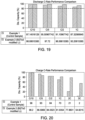
- FIGS. 16A-16B are plots depicting discharge capacity versus cycle number for a bare lithium metal anode and a lithium metal anode protected with Bi 2 Te 3 .
- Li/LiCoO 2 CR2032 coin cells with Bi 2 Te 3 modified Li as proof-of-concept platform to test the efficacy of the anode passivation procedure described herein.
- Full cells were made with Li metal as anode and commercial Lithium Cobalt oxide as the cathode with 1M LiPF 6 (EC: DEC 2% FEC) electrolytes. It was observed from FIG.
Landscapes
- Chemical & Material Sciences (AREA)
- Chemical Kinetics & Catalysis (AREA)
- Electrochemistry (AREA)
- General Chemical & Material Sciences (AREA)
- Engineering & Computer Science (AREA)
- Materials Engineering (AREA)
- Composite Materials (AREA)
- Manufacturing & Machinery (AREA)
- Battery Electrode And Active Subsutance (AREA)
- Secondary Cells (AREA)
- Cell Electrode Carriers And Collectors (AREA)
- Electric Double-Layer Capacitors Or The Like (AREA)
Claims (14)
- Procédé comprenant :la formation d'un film de lithium métallique sur un collecteur de courant, dans lequel le collecteur de courant comprend un film en cuivre ; etla formation d'un empilement de films SEI sur le film de lithium métallique, comprenant :l'exposition du film de lithium métallique à un traitement au gaz, le traitement au gaz comprenant l'exposition du film de lithium métallique à un traitement au gaz SF6, à un processus d'oxydation par plasma ou à un processus de nitruration par plasma ; etla formation d'un film de chalcogénure sur le film de lithium métallique, le film de chalcogénure étant choisi dans le groupe des films de chalcogénure de bismuth, de chalcogénure de cuivre ou des combinaisons de ces films
oula formation d'un empilement de films SEI sur le film de lithium métallique, comprenant :la formation d'un film de chalcogénure sur le film de lithium métallique, le film de chalcogénure étant choisi dans le groupe des films de chalcogénure de bismuth, de chalcogénure de cuivre ou des combinaisons de ces films ;la formation d'un film de lithium métallique supplémentaire sur le film de chalcogénure ; etl'exposition du film de lithium métallique supplémentaire à un traitement au gaz, le traitement au gaz comprenant l'exposition du film de lithium métallique à un traitement au gaz SF6, à un processus d'oxydation par plasma ou à un processus de nitruration par plasma. - Procédé selon la revendication 1, dans lequel l'empilement de films SEI comprend un film de fluorure de lithium (LiF), un film de carbonate de lithium (Li2CO3), un film d'oxyde de lithium, un film de nitrure de lithium (Li3N), ou des combinaisons de ceux-ci.
- Procédé selon la revendication 2, dans lequel le film de lithium métallique a une épaisseur comprise entre 1 et 20 micromètres.
- Procédé selon la revendication 3, dans lequel le collecteur de courant a une épaisseur comprise entre 2 micromètres et 8 micromètres.
- Procédé selon la revendication 1, dans lequel le collecteur de courant comprend :un premier film contenant du nickel ou du chrome ;un film en cuivre formé sur le premier film contenant du nickel ou du chrome et ayant une épaisseur comprise entre 50 nanomètres et 500 nanomètres ; etun second film contenant du nickel ou du chrome formé sur le film en cuivre et ayant une épaisseur comprise entre 20 nanomètres et 50 nanomètres.
- Procédé selon la revendication 1, dans lequel le collecteur de courant comprend :un substrat polymère de polyéthylène téréphtalate (PET) ; etun film en cuivre formé sur le substrat polymère PET, dans lequel le film en cuivre est déposé par l'intermédiaire d'un processus de dépôt physique en phase vapeur.
- Procédé selon la revendication 1, dans lequel le collecteur de courant comprenant le film en cuivre est exposé à un traitement au plasma ou à un processus de décharge à effet de couronne pour éliminer les matières organiques des surfaces exposées du collecteur de courant.
- Procédé selon la revendication 1, dans lequel le film de chalcogénure est déposé à l'aide d'un procédé de dépôt physique en phase vapeur (PVD) possédant une source d'énergie RF couplée à une cible composée des matériaux du film de chalcogénure.
- Procédé selon la revendication 8, comprenant en outre :
la formation d'un film d'oxyde de lithium sur le film de chalcogénure en déposant un film de lithium métallique supplémentaire par l'intermédiaire d'un processus PVD réalisé dans une atmosphère contenant de l'oxygène. - Structure d'électrode anode, comprenant :un collecteur de courant comprenant un film en cuivre ;un film de lithium métallique formé sur le collecteur de courant ; etun empilement de films d'interface d'électrolyte solide (SEI) formé sur le film de lithium métallique, comprenant :un film formé sur le film de lithium métallique par traitement au gaz, comprenant l'exposition du film de lithium métallique à un traitement au gaz SF6, à un processus d'oxydation par plasma ou à un processus de nitruration par plasma ; etun film de chalcogénure formé sur le film, le film de chalcogénure étant choisi dans le groupe des films de chalcogénure de bismuth, des films de chalcogénure de cuivre ou des combinaisons de ces films ;
ouun empilement de films d'interface d'électrolyte solide (SEI) formé sur le film de lithium métallique, comprenant :un film de chalcogénure formé sur le film de lithium métal, le film de chalcogénure étant choisi dans le groupe des films de chalcogénure de bismuth, de chalcogénure de cuivre ou des combinaisons de ceux-ciun film de lithium métallique supplémentaire formé sur le film de chalcogénure ; etun film formé sur le film de lithium métallique supplémentaire par traitement au gaz, comprenant l'exposition du film de lithium métallique à un traitement au gaz SF6, à un processus d'oxydation par plasma ou à un processus de nitruration par plasma. - Structure d'électrode anode selon la revendication 10, dans laquelle l'empilement de films SEI comprend en outre un film de fluorure de lithium formé sur le film de chalcogénure.
- Structure d'électrode anode selon la revendication 10, dans laquelle le film de chalcogénure est choisi dans le groupe CuS, Cu2Se, Cu2S, Cu2Te, CuTe, Bi2Te3, Bi2Se3, ou des combinaisons de ceux-ci.
- Structure d'électrode anode selon la revendication 10, dans laquelle l'empilement de films SEI comprend en outre un film d'oxyde de lithium formé sur le film de chalcogénure.
- Structure d'électrode anode selon la revendication 13, dans laquelle l'empilement de films SEI comprend en outre un film de carbonate de lithium formé sur le film d'oxyde de lithium.
Applications Claiming Priority (2)
| Application Number | Priority Date | Filing Date | Title |
|---|---|---|---|
| US201762583911P | 2017-11-09 | 2017-11-09 | |
| PCT/US2018/053894 WO2019094121A1 (fr) | 2017-11-09 | 2018-10-02 | Modification ex situ d'interface d'électrolyte solide à l'aide de chalcogénures pour anode métallique au lithium |
Publications (3)
| Publication Number | Publication Date |
|---|---|
| EP3707767A1 EP3707767A1 (fr) | 2020-09-16 |
| EP3707767A4 EP3707767A4 (fr) | 2021-08-18 |
| EP3707767B1 true EP3707767B1 (fr) | 2024-07-10 |
Family
ID=66327640
Family Applications (1)
| Application Number | Title | Priority Date | Filing Date |
|---|---|---|---|
| EP18876410.4A Active EP3707767B1 (fr) | 2017-11-09 | 2018-10-02 | Modification ex situ d'interface d'électrolyte solide à l'aide de chalcogénures pour anode métallique au lithium |
Country Status (6)
| Country | Link |
|---|---|
| US (3) | US10944103B2 (fr) |
| EP (1) | EP3707767B1 (fr) |
| JP (3) | JP7052035B2 (fr) |
| KR (3) | KR102591474B1 (fr) |
| CN (1) | CN111316478A (fr) |
| WO (1) | WO2019094121A1 (fr) |
Families Citing this family (25)
| Publication number | Priority date | Publication date | Assignee | Title |
|---|---|---|---|---|
| US20200407841A1 (en) * | 2018-02-07 | 2020-12-31 | Ulvac, Inc. | Thin film formation method, thin film formation apparatus, and lithium battery |
| US10910653B2 (en) | 2018-02-26 | 2021-02-02 | Graphenix Development, Inc. | Anodes for lithium-based energy storage devices |
| EP3939107A4 (fr) * | 2019-03-11 | 2023-06-21 | Coreshell Technologies, Inc. | Électrodéposition en phase solution de couches d'interphase d'électrolyte solide (sei) artificielle sur des électrodes de batterie |
| US11631840B2 (en) * | 2019-04-26 | 2023-04-18 | Applied Materials, Inc. | Surface protection of lithium metal anode |
| JP2020187932A (ja) * | 2019-05-15 | 2020-11-19 | 株式会社アルバック | リチウムイオン二次電池用負極の集電体の製造方法 |
| JP2020187929A (ja) * | 2019-05-15 | 2020-11-19 | 株式会社アルバック | リチウムイオン二次電池用負極の集電体 |
| US11024842B2 (en) * | 2019-06-27 | 2021-06-01 | Graphenix Development, Inc. | Patterned anodes for lithium-based energy storage devices |
| CA3148019A1 (fr) | 2019-08-13 | 2021-02-18 | John C. Brewer | Anodes pour dispositifs de stockage d'energie a base de lithium et procedes pour la fabrication de celles-ci |
| US11489154B2 (en) | 2019-08-20 | 2022-11-01 | Graphenix Development, Inc. | Multilayer anodes for lithium-based energy storage devices |
| US20210057755A1 (en) * | 2019-08-21 | 2021-02-25 | Graphenix Development, Inc. | Anodes for lithium-based energy storage devices |
| US11384419B2 (en) | 2019-08-30 | 2022-07-12 | Micromaierials Llc | Apparatus and methods for depositing molten metal onto a foil substrate |
| CN111697222A (zh) * | 2020-04-07 | 2020-09-22 | 电子科技大学 | 一种高能量密度锂电池电芯及其制备方法 |
| CN112421115B (zh) * | 2020-09-14 | 2022-11-18 | 上海大学 | 硒化铜原位包覆泡沫铜作为锂金属载体的锂金属基电池及其制备方法 |
| CA3195802A1 (fr) * | 2020-10-16 | 2022-04-21 | Timothy George JOHNSTON | Ensembles anodes metalliques au lithium et appareil et procede de fabrication |
| WO2022125441A1 (fr) * | 2020-12-10 | 2022-06-16 | Applied Materials, Inc. | Métrologie de bord de bande |
| EP4020612A1 (fr) * | 2020-12-24 | 2022-06-29 | Vito NV | Procédé d'application d'une couche de protection pour un métal alcalin ou une surface d'alliage de métal alcalin, et article comprenant ladite couche protectrice |
| WO2022204366A1 (fr) * | 2021-03-26 | 2022-09-29 | Sion Power Corporation | Commande in-situ d'interface d'électrolyte solide pour performance de cycle améliorée dans des batteries au lithium-métal |
| CA3219752A1 (fr) * | 2021-05-19 | 2022-11-24 | Maciej Urban JASTRZEBSKI | Ensembles anode au lithium metallique et appareil et leur procede de fabrication |
| US11769867B2 (en) * | 2021-07-26 | 2023-09-26 | Textron Innovations Inc. | Forming battery electrodes and associated battery |
| CN113363456B (zh) | 2021-08-09 | 2021-11-12 | 天津中能锂业有限公司 | 超薄锂膜复合体及其制备方法 |
| EP4425629A1 (fr) | 2021-10-29 | 2024-09-04 | Panasonic Intellectual Property Management Co., Ltd. | Batterie secondaire au lithium |
| WO2023164042A1 (fr) * | 2022-02-24 | 2023-08-31 | The Government Of The United States Of America, As Represented By The Secretary Of The Navy | Membrane à transport d'oxygène à basse température bixoysez nano-mince pour le transport d'oxygène, la séparation, et la manipulation de matériau bidimensionnel (2d) |
| DE102022203616B3 (de) | 2022-04-11 | 2023-08-31 | Volkswagen Aktiengesellschaft | Verfahren zur Fertigung einer Lithium-Ionen-Batteriezelle |
| WO2024015141A1 (fr) * | 2022-07-11 | 2024-01-18 | Applied Materials, Inc. | Procédés et systèmes de production d'anodes à lithium intercalé |
| US20240170639A1 (en) * | 2022-11-22 | 2024-05-23 | Li-Metal Corp. | Lithium weldments |
Family Cites Families (36)
| Publication number | Priority date | Publication date | Assignee | Title |
|---|---|---|---|---|
| US4299890A (en) | 1980-06-18 | 1981-11-10 | Duracell International Inc. | Solid state cell |
| JPH04248276A (ja) * | 1991-01-25 | 1992-09-03 | Matsushita Electric Ind Co Ltd | リチウム二次電池 |
| JPH11297359A (ja) * | 1998-04-15 | 1999-10-29 | Matsushita Electric Ind Co Ltd | 全固体リチウム二次電池 |
| JP4016344B2 (ja) * | 1998-12-03 | 2007-12-05 | 住友電気工業株式会社 | リチウム二次電池 |
| US7247408B2 (en) | 1999-11-23 | 2007-07-24 | Sion Power Corporation | Lithium anodes for electrochemical cells |
| AU1796701A (en) * | 1999-11-23 | 2001-06-04 | Moltech Corporation | Lithium anodes for electrochemical cells |
| CN1179432C (zh) * | 2001-05-31 | 2004-12-08 | 三星Sdi株式会社 | 锂电池的锂金属阳级保护层的形成方法 |
| KR100450208B1 (ko) | 2002-09-23 | 2004-09-24 | 삼성에스디아이 주식회사 | 리튬 전지용 음극 및 이를 포함하는 리튬 전지 |
| KR100508945B1 (ko) | 2003-04-17 | 2005-08-17 | 삼성에스디아이 주식회사 | 리튬 전지용 음극, 그의 제조 방법 및 그를 포함하는 리튬전지 |
| KR100542198B1 (ko) | 2003-10-23 | 2006-01-11 | 삼성에스디아이 주식회사 | 리튬 폴리머 이차 전지 |
| KR100542213B1 (ko) | 2003-10-31 | 2006-01-10 | 삼성에스디아이 주식회사 | 리튬 금속 전지용 음극 및 이를 포함하는 리튬 금속 전지 |
| US20090107834A1 (en) | 2007-10-29 | 2009-04-30 | Applied Materials, Inc. | Chalcogenide target and method |
| US20100156353A1 (en) * | 2008-12-18 | 2010-06-24 | Quantumsphere, Inc. | Lithium nanoparticle compositions for use in electrochemical applications |
| US9799914B2 (en) * | 2009-01-29 | 2017-10-24 | Corning Incorporated | Barrier layer for thin film battery |
| CN102449841A (zh) | 2009-06-29 | 2012-05-09 | 应用材料公司 | 能量储存装置中的三维含铜电极的固态电解质界面所用的钝化膜 |
| JP2012056549A (ja) | 2010-09-09 | 2012-03-22 | Tomoaki Koseki | 車両用タイヤ |
| EP2647066A1 (fr) | 2010-12-05 | 2013-10-09 | Ramot at Tel Aviv University, Ltd. | Dépôt électrophorétique de batteries en couches minces |
| US20120219841A1 (en) * | 2011-02-25 | 2012-08-30 | Applied Materials, Inc. | Lithium ion cell design apparatus and method |
| US8936870B2 (en) * | 2011-10-13 | 2015-01-20 | Sion Power Corporation | Electrode structure and method for making the same |
| KR20140097510A (ko) | 2011-11-30 | 2014-08-06 | 어플라이드 머티어리얼스, 인코포레이티드 | 폐쇄 루프 제어 |
| US20140001576A1 (en) | 2012-06-27 | 2014-01-02 | Applied Materials, Inc. | Lowering tungsten resistivity by replacing titanium nitride with titanium silicon nitride |
| KR20160002988A (ko) | 2013-04-23 | 2016-01-08 | 어플라이드 머티어리얼스, 인코포레이티드 | 고체 및 액체 전해질들을 갖는 전기화학 셀 |
| EP2863291A1 (fr) | 2013-10-18 | 2015-04-22 | Applied Materials, Inc. | Corps transparent pour procédé de fabrication de panneau tactile et système de fabrication d'un corps transparent pour un tel panneau |
| US9985293B2 (en) * | 2014-07-10 | 2018-05-29 | The Board Of Trustees Of The Leland Stanford Junior University | Structure that encapsulates lithium metal for high energy density battery anode |
| US10256448B2 (en) * | 2014-07-10 | 2019-04-09 | The Board Of Trustees Of The Leland Stanford Junior University | Interfacial engineering for stable lithium metal anodes |
| EP3198670B1 (fr) | 2014-09-23 | 2020-10-28 | Applied Materials, Inc. | Cellule électrochimique à électrode négative protégée |
| KR101984719B1 (ko) * | 2014-10-23 | 2019-05-31 | 주식회사 엘지화학 | 다층구조의 리튬금속 전극 및 이의 제조방법 |
| CN107210412A (zh) * | 2015-01-09 | 2017-09-26 | 应用材料公司 | 电池分隔件上的锂金属涂层 |
| JP6573312B2 (ja) | 2015-06-22 | 2019-09-11 | 日産自動車株式会社 | リチウムイオン二次電池用集電体 |
| US10763512B2 (en) * | 2015-08-28 | 2020-09-01 | Toyota Motor Engineering & Manufacturing North America, Inc. | Lithium deposition with multilayer nanomebrane |
| CN108604668B (zh) | 2016-01-28 | 2022-07-08 | 应用材料公司 | 具有保护层工具的整合的锂沉积 |
| JP2017182905A (ja) | 2016-03-28 | 2017-10-05 | 古河電気工業株式会社 | タブリード付き負極集電銅箔およびこのタブリード付き負極集電銅箔を有する電池 |
| JP2019522879A (ja) | 2016-06-21 | 2019-08-15 | アプライド マテリアルズ インコーポレイテッドApplied Materials,Incorporated | 改善されたリチウム金属サイクリングのための中間相層 |
| CN106803580A (zh) * | 2017-01-19 | 2017-06-06 | 浙江大学 | 一种用于锂金属电池的负极材料 |
| CN107154499B (zh) | 2017-04-14 | 2020-05-15 | 宁德时代新能源科技股份有限公司 | 一种含有集流体的锂电池及其制备方法 |
| EP3685460B1 (fr) | 2017-09-21 | 2024-05-15 | Applied Materials, Inc. | Fabrication d'empilements de dispositifs d'anodes au lithium |
-
2018
- 2018-10-02 US US16/150,111 patent/US10944103B2/en active Active
- 2018-10-02 EP EP18876410.4A patent/EP3707767B1/fr active Active
- 2018-10-02 CN CN201880071709.7A patent/CN111316478A/zh active Pending
- 2018-10-02 KR KR1020237009085A patent/KR102591474B1/ko active IP Right Grant
- 2018-10-02 JP JP2020524784A patent/JP7052035B2/ja active Active
- 2018-10-02 WO PCT/US2018/053894 patent/WO2019094121A1/fr unknown
- 2018-10-02 KR KR1020207016035A patent/KR102512001B1/ko active IP Right Grant
- 2018-10-02 KR KR1020237035293A patent/KR102643656B1/ko active IP Right Grant
-
2021
- 2021-03-08 US US17/194,899 patent/US11462733B2/en active Active
-
2022
- 2022-03-30 JP JP2022055933A patent/JP7383749B2/ja active Active
- 2022-09-07 US US17/939,121 patent/US11735723B2/en active Active
-
2023
- 2023-11-08 JP JP2023190502A patent/JP2024023248A/ja active Pending
Also Published As
| Publication number | Publication date |
|---|---|
| JP2022104957A (ja) | 2022-07-12 |
| KR20230148279A (ko) | 2023-10-24 |
| JP2021502671A (ja) | 2021-01-28 |
| US11462733B2 (en) | 2022-10-04 |
| KR102512001B1 (ko) | 2023-03-21 |
| JP2024023248A (ja) | 2024-02-21 |
| EP3707767A1 (fr) | 2020-09-16 |
| KR102643656B1 (ko) | 2024-03-05 |
| US20230006197A1 (en) | 2023-01-05 |
| KR20230041092A (ko) | 2023-03-23 |
| JP7052035B2 (ja) | 2022-04-11 |
| JP7383749B2 (ja) | 2023-11-20 |
| KR20200068752A (ko) | 2020-06-15 |
| US20210210752A1 (en) | 2021-07-08 |
| US20190140267A1 (en) | 2019-05-09 |
| EP3707767A4 (fr) | 2021-08-18 |
| US10944103B2 (en) | 2021-03-09 |
| KR102591474B1 (ko) | 2023-10-20 |
| CN111316478A (zh) | 2020-06-19 |
| WO2019094121A1 (fr) | 2019-05-16 |
| US11735723B2 (en) | 2023-08-22 |
Similar Documents
| Publication | Publication Date | Title |
|---|---|---|
| US11462733B2 (en) | Ex-situ solid electrolyte interface modification using chalcogenides for lithium metal anode | |
| US11888109B2 (en) | Lithium anode device stack manufacturing | |
| US11817576B2 (en) | Integrated lithium deposition with protective layer tool | |
| TWI689128B (zh) | 用於改良的鋰金屬循環的介面層 | |
| WO2024073001A1 (fr) | Réduction d'oxyde et d'hydroxyde de métal alcalin dans le film par couche passivée de surface ex situ | |
| WO2024091411A1 (fr) | Revêtement protecteur multicouche pour anodes en lithium métallique |
Legal Events
| Date | Code | Title | Description |
|---|---|---|---|
| STAA | Information on the status of an ep patent application or granted ep patent |
Free format text: STATUS: THE INTERNATIONAL PUBLICATION HAS BEEN MADE |
|
| PUAI | Public reference made under article 153(3) epc to a published international application that has entered the european phase |
Free format text: ORIGINAL CODE: 0009012 |
|
| STAA | Information on the status of an ep patent application or granted ep patent |
Free format text: STATUS: REQUEST FOR EXAMINATION WAS MADE |
|
| 17P | Request for examination filed |
Effective date: 20200608 |
|
| AK | Designated contracting states |
Kind code of ref document: A1 Designated state(s): AL AT BE BG CH CY CZ DE DK EE ES FI FR GB GR HR HU IE IS IT LI LT LU LV MC MK MT NL NO PL PT RO RS SE SI SK SM TR |
|
| AX | Request for extension of the european patent |
Extension state: BA ME |
|
| DAV | Request for validation of the european patent (deleted) | ||
| DAX | Request for extension of the european patent (deleted) | ||
| A4 | Supplementary search report drawn up and despatched |
Effective date: 20210720 |
|
| RIC1 | Information provided on ipc code assigned before grant |
Ipc: H01M 4/1395 20100101AFI20210714BHEP Ipc: H01M 4/134 20100101ALI20210714BHEP Ipc: H01M 4/62 20060101ALI20210714BHEP Ipc: H01M 4/66 20060101ALI20210714BHEP Ipc: H01M 10/052 20100101ALI20210714BHEP Ipc: H01M 4/38 20060101ALI20210714BHEP Ipc: H01M 4/04 20060101ALI20210714BHEP Ipc: H01M 4/36 20060101ALI20210714BHEP |
|
| STAA | Information on the status of an ep patent application or granted ep patent |
Free format text: STATUS: EXAMINATION IS IN PROGRESS |
|
| 17Q | First examination report despatched |
Effective date: 20230222 |
|
| GRAP | Despatch of communication of intention to grant a patent |
Free format text: ORIGINAL CODE: EPIDOSNIGR1 |
|
| STAA | Information on the status of an ep patent application or granted ep patent |
Free format text: STATUS: GRANT OF PATENT IS INTENDED |
|
| INTG | Intention to grant announced |
Effective date: 20240205 |
|
| GRAS | Grant fee paid |
Free format text: ORIGINAL CODE: EPIDOSNIGR3 |
|
| GRAA | (expected) grant |
Free format text: ORIGINAL CODE: 0009210 |
|
| STAA | Information on the status of an ep patent application or granted ep patent |
Free format text: STATUS: THE PATENT HAS BEEN GRANTED |
|
| AK | Designated contracting states |
Kind code of ref document: B1 Designated state(s): AL AT BE BG CH CY CZ DE DK EE ES FI FR GB GR HR HU IE IS IT LI LT LU LV MC MK MT NL NO PL PT RO RS SE SI SK SM TR |
|
| REG | Reference to a national code |
Ref country code: CH Ref legal event code: EP |
|
| REG | Reference to a national code |
Ref country code: DE Ref legal event code: R096 Ref document number: 602018071702 Country of ref document: DE |