EP3672220A1 - Fotoempfindliche anordnung, bilderzeugungsmodul, intelligentes endgerät und verfahren und form zur herstellung einer lichtempfindlichen anordnung - Google Patents
Fotoempfindliche anordnung, bilderzeugungsmodul, intelligentes endgerät und verfahren und form zur herstellung einer lichtempfindlichen anordnung Download PDFInfo
- Publication number
- EP3672220A1 EP3672220A1 EP18845725.3A EP18845725A EP3672220A1 EP 3672220 A1 EP3672220 A1 EP 3672220A1 EP 18845725 A EP18845725 A EP 18845725A EP 3672220 A1 EP3672220 A1 EP 3672220A1
- Authority
- EP
- European Patent Office
- Prior art keywords
- top surface
- lamination
- photosensitive
- mould
- molded
- Prior art date
- Legal status (The legal status is an assumption and is not a legal conclusion. Google has not performed a legal analysis and makes no representation as to the accuracy of the status listed.)
- Granted
Links
Images






Classifications
-
- H—ELECTRICITY
- H10—SEMICONDUCTOR DEVICES; ELECTRIC SOLID-STATE DEVICES NOT OTHERWISE PROVIDED FOR
- H10W—GENERIC PACKAGES, INTERCONNECTIONS, CONNECTORS OR OTHER CONSTRUCTIONAL DETAILS OF DEVICES COVERED BY CLASS H10
- H10W74/00—Encapsulations, e.g. protective coatings
- H10W74/10—Encapsulations, e.g. protective coatings characterised by their shape or disposition
-
- H—ELECTRICITY
- H10—SEMICONDUCTOR DEVICES; ELECTRIC SOLID-STATE DEVICES NOT OTHERWISE PROVIDED FOR
- H10F—INORGANIC SEMICONDUCTOR DEVICES SENSITIVE TO INFRARED RADIATION, LIGHT, ELECTROMAGNETIC RADIATION OF SHORTER WAVELENGTH OR CORPUSCULAR RADIATION
- H10F39/00—Integrated devices, or assemblies of multiple devices, comprising at least one element covered by group H10F30/00, e.g. radiation detectors comprising photodiode arrays
- H10F39/80—Constructional details of image sensors
- H10F39/804—Containers or encapsulations
-
- H—ELECTRICITY
- H04—ELECTRIC COMMUNICATION TECHNIQUE
- H04N—PICTORIAL COMMUNICATION, e.g. TELEVISION
- H04N23/00—Cameras or camera modules comprising electronic image sensors; Control thereof
- H04N23/50—Constructional details
- H04N23/54—Mounting of pick-up tubes, electronic image sensors, deviation or focusing coils
-
- B—PERFORMING OPERATIONS; TRANSPORTING
- B29—WORKING OF PLASTICS; WORKING OF SUBSTANCES IN A PLASTIC STATE IN GENERAL
- B29C—SHAPING OR JOINING OF PLASTICS; SHAPING OF MATERIAL IN A PLASTIC STATE, NOT OTHERWISE PROVIDED FOR; AFTER-TREATMENT OF THE SHAPED PRODUCTS, e.g. REPAIRING
- B29C45/00—Injection moulding, i.e. forcing the required volume of moulding material through a nozzle into a closed mould; Apparatus therefor
- B29C45/14—Injection moulding, i.e. forcing the required volume of moulding material through a nozzle into a closed mould; Apparatus therefor incorporating preformed parts or layers, e.g. injection moulding around inserts or for coating articles
- B29C45/14336—Coating a portion of the article, e.g. the edge of the article
-
- B—PERFORMING OPERATIONS; TRANSPORTING
- B29—WORKING OF PLASTICS; WORKING OF SUBSTANCES IN A PLASTIC STATE IN GENERAL
- B29C—SHAPING OR JOINING OF PLASTICS; SHAPING OF MATERIAL IN A PLASTIC STATE, NOT OTHERWISE PROVIDED FOR; AFTER-TREATMENT OF THE SHAPED PRODUCTS, e.g. REPAIRING
- B29C45/00—Injection moulding, i.e. forcing the required volume of moulding material through a nozzle into a closed mould; Apparatus therefor
- B29C45/17—Component parts, details or accessories; Auxiliary operations
- B29C45/26—Moulds
- B29C45/37—Mould cavity walls, i.e. the inner surface forming the mould cavity, e.g. linings
-
- H—ELECTRICITY
- H04—ELECTRIC COMMUNICATION TECHNIQUE
- H04N—PICTORIAL COMMUNICATION, e.g. TELEVISION
- H04N23/00—Cameras or camera modules comprising electronic image sensors; Control thereof
- H04N23/50—Constructional details
-
- H—ELECTRICITY
- H04—ELECTRIC COMMUNICATION TECHNIQUE
- H04N—PICTORIAL COMMUNICATION, e.g. TELEVISION
- H04N23/00—Cameras or camera modules comprising electronic image sensors; Control thereof
- H04N23/50—Constructional details
- H04N23/55—Optical parts specially adapted for electronic image sensors; Mounting thereof
-
- H—ELECTRICITY
- H10—SEMICONDUCTOR DEVICES; ELECTRIC SOLID-STATE DEVICES NOT OTHERWISE PROVIDED FOR
- H10F—INORGANIC SEMICONDUCTOR DEVICES SENSITIVE TO INFRARED RADIATION, LIGHT, ELECTROMAGNETIC RADIATION OF SHORTER WAVELENGTH OR CORPUSCULAR RADIATION
- H10F39/00—Integrated devices, or assemblies of multiple devices, comprising at least one element covered by group H10F30/00, e.g. radiation detectors comprising photodiode arrays
- H10F39/011—Manufacture or treatment of image sensors covered by group H10F39/12
-
- H—ELECTRICITY
- H10—SEMICONDUCTOR DEVICES; ELECTRIC SOLID-STATE DEVICES NOT OTHERWISE PROVIDED FOR
- H10F—INORGANIC SEMICONDUCTOR DEVICES SENSITIVE TO INFRARED RADIATION, LIGHT, ELECTROMAGNETIC RADIATION OF SHORTER WAVELENGTH OR CORPUSCULAR RADIATION
- H10F39/00—Integrated devices, or assemblies of multiple devices, comprising at least one element covered by group H10F30/00, e.g. radiation detectors comprising photodiode arrays
- H10F39/80—Constructional details of image sensors
- H10F39/806—Optical elements or arrangements associated with the image sensors
- H10F39/8063—Microlenses
-
- B—PERFORMING OPERATIONS; TRANSPORTING
- B29—WORKING OF PLASTICS; WORKING OF SUBSTANCES IN A PLASTIC STATE IN GENERAL
- B29C—SHAPING OR JOINING OF PLASTICS; SHAPING OF MATERIAL IN A PLASTIC STATE, NOT OTHERWISE PROVIDED FOR; AFTER-TREATMENT OF THE SHAPED PRODUCTS, e.g. REPAIRING
- B29C2793/00—Shaping techniques involving a cutting or machining operation
- B29C2793/009—Shaping techniques involving a cutting or machining operation after shaping
-
- B—PERFORMING OPERATIONS; TRANSPORTING
- B29—WORKING OF PLASTICS; WORKING OF SUBSTANCES IN A PLASTIC STATE IN GENERAL
- B29L—INDEXING SCHEME ASSOCIATED WITH SUBCLASS B29C, RELATING TO PARTICULAR ARTICLES
- B29L2011/00—Optical elements, e.g. lenses, prisms
Definitions
- the present disclosure relates to the technical field of imaging assemblies and smart terminals, and in particular, to a photosensitive assembly, an imaging module, a smart terminal, and a method and a mould for manufacturing a photosensitive assembly.
- Molded camera modules are a very popular high-tech in the current market. Instead of an ordinary lens holder, a photosensitive chip, a connecting medium and an electronic component of a camera module are encapsulated and fixed on a circuit board by molding, obtaining good impact stability and thermal stability.
- the upper surface of the molding structure is very flat, which can improve the tilt accuracy of mounting a lens or motor above the chip.
- the flat upper surface also brings new problems.
- the lens or motor above the molding structure still needs to apply glue and the glue is cured by drastic changes in the external environment such as exposure or heating. On the one hand, the glue has certain fluidity.
- the flat surface for mounting optical assemblies in the molded portion has become smaller and smaller.
- the lens or motor has a high requirement for mounting tilt accuracy, how to maintain miniaturization of the camera module while providing a mounting plane as large as possible on the molded portion is also an issue that needs to be solved urgently.
- a photosensitive assembly characterized in that it comprises: a circuit board having a rectangular-shaped rigid board region and comprising a flexible board extension portion extending from the rigid board region, wherein the rigid board region has a lamination side and a non-lamination side, the rigid board region has a lamination region on the lamination side, and the flexible board extension portion extends out from the lamination side; a photosensitive element mounted in the rigid board region of the circuit board; and a molded portion formed on the rigid board region, surrounding the photosensitive element, and extending towards the photosensitive element and coming into contact with the photosensitive element, wherein the molded portion has an inner side surface, an outer side surface and a top surface, the molded portion does not cover the lamination region of the rigid board region, and the top surface has a flat portion, wherein the top surface of a part of the molded portion on the lamination side has a descending portion, the descending portion is located between the flat portion and the outer side surface of the molded portion
- the descending portion in a first section therethrough, has a contour of a first arc shape, wherein the first section is in a plane perpendicular to an edge of the rigid board region on the lamination side.
- the molded portion comprises a connecting portion connecting the inner side surface and the flat portion.
- the connecting portion in a second section therethrough, has a contour of a second arc shape, wherein the second section is in a plane perpendicular to the flat portion adjacent to the connecting portion and the inner side surface, and a length of the first arc shape is greater than a length of the second arc shape.
- the connecting portion in a second section therethrough, has a contour of a second arc shape, wherein the second section is in a plane perpendicular to the flat portion adjacent to the connecting portion and the inner side surface, and a radius of curvature of the first arc shape is greater than a radius of curvature of the second arc shape.
- the top surface of the molded portion has a recessed portion adjacent to the connecting portion, and the recessed portion, in a third section therethrough, has a contour of a right angle shape, and the right angle shape has a side parallel to the flat portion of the molded portion, wherein the third section is in a plane perpendicular to the inner side surface and the top surface of the molded portion.
- An outer side surface of the molded portion has a recessed portion adjacent to the descending portion, and the recessed portion, in a third section therethrough, has a contour of an arc shape, a right angle shape, or an oblique line shape, wherein the third section is in a plane perpendicular to an edge of the rigid board region on the lamination side.
- the molded portion has an opening exposing the photosensitive element.
- the inner side surface of the molded portion is at an obtuse angle with a top surface of the photosensitive element.
- the inner side surface of the molded portion is directly connected to a top surface of the photosensitive element.
- an imaging module characterized in that it comprises the photosensitive assembly described above and an optical assembly mounted on the photosensitive assembly.
- the optical assembly is connected to the top surface of the molded portion by an adhesive, wherein the adhesive is present on the descending portion.
- the optical assembly comprises a filter assembly, a lens assembly, and a driving element.
- the optical assembly comprises a lens assembly, and the lens assembly is connected to the flat portion of the top surface of the molded portion by an adhesive.
- a smart terminal comprising the imaging module described above.
- the attaching the flexible film to the mould comprises: attaching the flexible film to the mould by evacuating gas between the flexible film and the mould.
- the mould has a protruded portion at an intersection between the top surface and the side surface of the cavity-shaped portion.
- the protruded portion in a first section therethrough, has a contour of an arc shape, an oblique line shape, or a right angle shape, wherein the first section is in a plane perpendicular to an edge of a corresponding one of the rigid board regions on the lamination side.
- the top surface of the cavity-shaped portion comprises a protruded portion closest to the respective indenter.
- the protruded portion has a bottom surface and a side surface, wherein the bottom surface is parallel to the top surface of the cavity-shaped portion.
- a side surface of the indenter forms an obtuse angle with the top surface of the cavity-shaped portion.
- a molding mould characterized in that it comprises a plurality of indenters arranged in an array and a cavity-shaped portion surrounding the plurality of indenters, wherein the respective cavity-shaped portion has a side surface and a flat top surface, and the side surface and the top surface form an open space with the indenters.
- the molding mould has a protruded portion at an intersection between the top surface and the side surface of the cavity-shaped portion.
- the protruded portion in a first section therethrough, has a contour of an arc shape, an oblique line shape, or a right angle shape, wherein the first section is in a plane perpendicular to the top surface and the side surface of the cavity-shaped portion.
- the top surface of the cavity-shaped portion comprises a protruded portion closest to the respective indenter.
- the protruded portion has a bottom surface and a side surface, wherein the bottom surface is parallel to the top surface of the cavity-shaped portion.
- a side surface of the indenter forms an obtuse angle with the top surface of the cavity-shaped portion.
- the photosensitive assembly provided by the present disclosure and the photosensitive assembly manufactured by using the method of the present disclosure can provide a relatively large glue overflow space so that the photosensitive assembly has a stable external size, and provide a flat top surface as large as possible in the molded portion while providing the glue overflow space.
- the flat top surface can facilitate automatic alignment of components mounted above it, and enhance the lateral bonding strength of the components mounted above it.
- first, second, etc. are only used to distinguish one feature from another feature, and do not indicate any limitation on the feature. Therefore, without departing from the teachings of the present application, a first main body discussed below may also be referred to as a second main body.
- the terms “substantially”, “approximately” and similar terms are used as a term expressing an approximation and not as a term expressing an extent, and are intended to indicate an inherent deviation in a measurement value or calculated value, which will be recognized by an ordinary person skilled in the art.
- spatially relative terms such as “under”, “below”, “lower”, “above”, “upper”, etc. may be used herein for descriptive purposes, and thus may be used to describe a relationship of an element or feature shown in the accompanying drawings with another element (multiple elements) or feature (multiple features).
- spatially relative terms are intended to include different orientations of a device in use, operation, and/or manufacturing. For example, if the device in the accompanying drawings is turned over, elements described as “under” or “below” other elements or features would then be oriented “above” the other elements or features.
- the exemplary term “below” may include both orientations of above and below.
- the device may be oriented in other ways (e.g., being rotated by 90 degrees or at other orientations), and thus spatially relative descriptors used herein are interpreted accordingly.
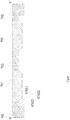
- Fig. 1 shows a top view of a photosensitive assembly according to an embodiment of the present disclosure
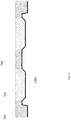
- Fig. 2 shows a sectional view of the photosensitive assembly taken along a line I-I' in Fig. 1 according to the embodiment of the present disclosure
- Fig. 3 shows an exploded perspective view of the photosensitive assembly in Fig. 1 according to the embodiment of the present disclosure.
- the photosensitive assembly 100 includes a circuit board 101, a photosensitive element 102, and a molded portion 103.
- the circuit board 101 may have a multilayer structure, for example, a multilayer structure stacked in an order of a rigid board, a flexible board, and a rigid board, but the present disclosure is not limited thereto.
- the circuit board 101 includes a rectangular rigid board region 104 and a flexible board extension portion 105 extending from one side of the rigid board region 104.
- a side to which the flexible board extension portion 105 is connected may be referred to as a flexible board side
- the flexible board extension portion 105 extends along a Y-axis direction
- the flexible board side of the rigid board region 104 extends along an X axis.
- the other side of the rigid board region 104 that is not connected to the flexible board extension portion 105 may be referred to as a non-flexible board side.
- the circuit board 101 has a lamination region 108 on the flexible board side of the rigid board region 104, and the lamination region 108 is located on the flexible board side of the circuit board 101 and is not covered by the molded portion 103.
- the photosensitive element 102 may be mounted on the circuit board 101, for example, may be mounted at a central position of the rigid board region 104, but the present disclosure is not limited thereto.
- the photosensitive element 102 can be used to convert light into an electrical signal.
- the molded portion 103 may be formed on the rigid board region 104 to surround the photosensitive element 102 and extend towards and come into contact with the photosensitive element 102.
- the molded portion 103 has an inner side surface S1031, an outer side surface S1032, and a top surface S1033 (refer to Fig. 3 ), and the molded portion 103 does not cover the lamination region 108.
- the top surface S1033 has a flat portion 106, the flat portion 106 is a flat part in the top surface S1033 of the molded portion 103, and this part is used to mount an assembly having high requirements on stability and flatness of the mounting plane, such as a lens assembly or a filter assembly.
- the flat portion 106 may be present on the top surface S1033 of the molded portion 103 located around the photosensitive element 102.
- the inner side surface S1031 and the outer side surface S1032 of the molded portion 103 surround the photosensitive element 102.
- the top surface S1033 of a part of the molded portion 103 on the lamination side has a descending portion 107, and the descending portion 107 is located between the flat portion 106 of the top surface S1033 and the outer side surface S1032 and is lower than the flat portion 106.
- the descending portion 107 may be a part between points a and b, wherein point a is a position where an extension plane (denoted by a dotted line inclined relative to a Z axis) of the outer side surface S1032 intersects with the molded portion 103, and point b is a position where an extension plane of the flat portion 106 (denoted by a dotted line parallel to the Y axis in part A of Fig. 2 ) intersects with the molded portion 103.
- the descending portion 107 is lower than the flat portion 106, when the optical assembly is mounted on the molded portion 103 by an adhesive, the descending portion 107 can accommodate the adhesive overflowing between the flat portion 106 and the optical assembly to function as a glue overflow groove.
- the descending portion 107 can provide a relatively large glue overflow space, so that the photosensitive assembly 100 can have a stable external size.
- the molded portion 103 may have a homocentric square shape, and the molded portion 103 has an opening in the middle to expose the photosensitive element 102. In a part of the molded portion 103 on the non-lamination side, the molded portion 103 may not have the descending portion 107, and the outer side surface S1032 of the molded portion 103 is perpendicular to the flat portion 106. As shown in Fig. 2 , in a part of the molded portion 103 farthest from the lamination region 108 in the Y direction, the outer side surface S1032 of the molded portion 103 is perpendicular to the flat portion 106.
- the outer side surface S1032 of the molded portion 103 may be perpendicular to the flat portion 106. This arrangement can provide a flat top surface as large as possible while having a descending portion in a part of the top surface to accommodate the overflown glue.
- Fig. 2 shows a sectional view of the photosensitive assembly taken along the line I-I' in Fig. 1 according to the embodiment of the present disclosure.
- the line I-I' extends along the Y direction and is perpendicular to an edge of the rigid board region 104 on the lamination side.
- a contour of the descending portion 107 may have a first arc shape, and the first arc shape may have a first length, i.e. an arc length from point a to point b.
- the connecting portion 109 may be a part between point c and point d, wherein point c is a position where the extension plane of the flat portion 106 intersects with the molded portion 103, and point d is a position where the extension plane of the inner side surface S1031 intersects with the molded portion 103.
- the connecting portion 109 has a second arc shape, and the second arc shape has a second length, i.e. an arc length from point c to point d.
- the descending portion 107 may have a first radius of curvature
- the connecting portion 109 may have a second radius of curvature
- the first arc length may be greater than the second arc length, or the first radius of curvature may be greater than the second radius of curvature.
- the first arc shape and the second arc shape may be a part of a circle or have a varying radius of curvature.
- the first radius of curvature or the second radius of curvature may be an average radius of curvature.
- a surface of the molded portion 103 composed of the descending portion 107, the flat portion 106, and the connecting portion 109 together makes the fluid thereon more inclined to flow towards the descending portion 107, because the descending portion 107 has a larger radius of curvature and a longer length, the tension of the fluid at the descending portion 107 is smaller, and it tends to flow towards the descending portion 107.
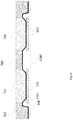
- Fig. 4 shows a sectional view of a photosensitive assembly taken along the line I-I' in FIG. 1 according to an exemplary embodiment of the present disclosure.
- the outer side surface S1032 of the molded portion 103 may have a recessed portion 110 adjacent to the descending portion 107.
- the enlarged views A-C in Fig. 4 each show three embodiments of the recessed portion 110.
- the sectional contour of the recessed portion 110 may have a right angle shape, an arc shape, or an oblique line shape.
- the outer side surface S1032 of the molded portion 103 further includes a recessed portion 110 to enable a larger glue overflow space provided so as to better accommodate the adhesive flowing out between the molded portion 103 and the optical element mounted thereon during the manufacturing process.
- Fig. 5 shows a sectional view of a photosensitive assembly taken along the line I-I' in Fig. 1 according to an exemplary embodiment of the present disclosure, wherein the enlarged view A in Fig. 5 corresponds to a part shown by a dotted circle in a lower sectional view of Fig. 5 .
- the top surface S1033 of the molded portion 103 has a recessed portion 111 adjacent to the connecting portion 109.
- the sectional contour of the recessed portion 111 may have a right angle shape, and the right angle shape has a side parallel to the flat portion 106 of the molded portion 103. That is, the recessed portion 111 has a platform parallel to the flat portion 106, and the platform is used for mounting an optical element having high requirements of flatness and stability, such as a filter assembly.
- the inner side surface S1031 of the molded portion 103 may be at an obtuse angle with the top surface of the photosensitive element 102.
- the inner side surface S1031 of the molded portion 103 may direct light incident thereon to reflect towards a direction away from the photosensitive element 102, so that the stray light incident on the photosensitive element 102 can be effectively reduced.
- the inner side surface S1031 of the molded portion 103 may be directly connected to the top surface of the photosensitive element 102. In this case, since there are no intermediate elements between the inner side surface S1031 of the molded portion 103 and the top surface of the photosensitive element 102, the thickness and volume of the photosensitive assembly 100 can be reduced.
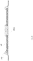
- FIG. 6 shows an imaging module according to an embodiment of the present disclosure.
- the imaging module 600 includes the photosensitive assembly 100 described with reference to Figs. 1 to 5 and an optical assembly 601 mounted on the photosensitive assembly 100.
- the optical assembly 601 is connected to the top surface of the molded portion 103 of the photosensitive assembly 100 by an adhesive 602, wherein the optical assembly 601 may be a filter assembly, a lens assembly, a driving element such as a motor, and the like.
- the enlarged view A in Fig. 6 corresponds to a part shown by a dotted circle in the right part of Fig. 6 . Referring to the enlarged view A in Fig.
- the adhesive 602 may be present on the descending portion 107 of the molded portion 103 due to the function of the glue overflow groove of the descending portion 107.
- the optical assembly 601 is a lens assembly
- the optical assembly 601 is connected to the flat portion of the molded portion 103 by the adhesive 602 because the lens assembly requires a higher flatness of the mounting plane.
- the mounting area for the lens assembly is increased, and the mounting plane of the lens assembly can be fully carried.
- the above imaging module 600 may be used in a smart terminal, for example, a smart phone, a tablet computer, and a wearable device such as a smart watch, and the like, but the present disclosure is not limited thereto.
- the imaging module 600 may be included in a camera of the smart phone.
- Fig. 7 shows a perspective view of a molding mould 700 according to an embodiment of the present disclosure.
- Fig. 8 shows a sectional view of the molding mould 700 taken along a line II-II' in Fig. 7 according to the embodiment of the present disclosure.
- the molding mould 700 may include a plurality of indenters 701 arranged in an array and a cavity-shaped portion 702 surrounding the plurality of indenters 701.
- the respective cavity-shaped portion 702 has a side surface S7021 and a flat top surface S7022, and the side surface S7021 and the top surface S7022 form an open space with the indenters 701.
- a shape formed by the top surface S7022 and the side surface S7021 of the cavity-shaped portion 702 and the side surface S7011 of the indenter 701 together corresponds to a part of the molded portion 103 on the lamination side in Fig. 2 .
- the side surface S7011 of the indenter 701 is at an obtuse angle with the top surface S7022 of the cavity-shaped portion 702 for forming the inner side surface S1031 of the molded portion 103 at an obtuse angle with the top surface of the photosensitive element 102 shown in Fig. 2 .
- Fig. 9 shows a sectional view of the molding mould 700 taken along the line II-II' in Fig. 7 according to an embodiment of the present disclosure, and the sectional view is perpendicular to the top surface S7022 and the side surface S7021 of the cavity-shaped portion 702.
- the molding mould 700 has a protruded portion 704 located at an intersection between the top surface S7022 and the side surface S7021 of the cavity-shaped portion 702. As shown in Fig.
- the sectional contour of the protruded portion 704 may have an arc shape, an oblique line shape, or a right angle shape, wherein in the sectional view including the indenter 701 and the cavity-shaped portion 702 in Fig. 9 , the sectional contour of the protruded portion 704 is shown as a right angle shape, and the protruded portions 704 having a sectional contour of an arc shape and an oblique line shape are shown in the enlarged views A and B in a lower part of Fig. 9 .
- the protruded portion 704 having the right angle shape is used to manufacture the recessed portion 110 shown in the enlarged view A of Fig. 4
- the protruded portions 704 having the sectional contours of the arc shape and the oblique line shape are used to manufacture the recessed portions 110 respectively shown in the enlarged views B and C of Fig. 4 .
- Fig. 10 shows a sectional view of the molding mould 700 taken along a line II-II' in Fig. 7 according to the embodiment of the present disclosure.
- an enlarged view of the protruded portion 705 is shown in the enlarged view A of Fig. 10 .
- the top surface S7022 of the cavity-shaped portion 702 includes a protruded portion 705 closest to the respective indenter 701.
- the protruded portion 705 has a bottom surface S7051 and a side surface S7052, wherein the bottom surface S7051 is parallel to the top surface S7022 of the cavity-shaped portion 702.
- the protruded portion 705 is used to form a recessed portion 111 shown in Fig. 5 .
- the protrusions 705 may surround the indenter 701.
- Fig. 11 shows a flowchart of a method 1100 for manufacturing the photosensitive assembly 100. As shown in Fig. 11 , the method 1100 for manufacturing the photosensitive assembly 100 may include steps 1101-1106.
- a plurality of photosensitive elements are mounted on a plurality of circuit boards in a CB-jointed panel, respectively.
- Fig. 12 shows a CB-jointed panel 1200 having a plurality of circuit boards 1201, wherein the circuit boards 1201 are arranged in an array and include rigid board regions 104 (see Fig. 3 ), the rigid board regions 104 have a lamination side and a non-lamination side, and a part of the circuit boards 1201 arranged in an array are shown by a dotted line in Fig. 12 .
- the circuit board 1201 may be a combined flexible and rigid board.
- a flexible film is attached to a mould, wherein the mould may be the molding mould 700 described with reference to Figs. 7-10 .
- Fig. 13 shows a sectional view of a molding mould 700 having a flexible film 1301 adsorbed and attached thereon, and the sectional view may correspond to the sectional view of the molding mould 700 shown in Fig. 8 .
- the flexible film 1301 can be attached to the molding mould 700 by means of vacuum adsorption.
- the gas between the flexible film 1301 and the mould 700 can be evacuated to form a vacuum, so that the flexible film 1301 is attached to the molding mould 700 and a shape corresponding to a bottom surface of the molding mould 700 is formed.
- the flexible film 1301 at an intersection of the side surface S7021 and the top surface S7022 (see Fig. 8 ) of the cavity-shaped portion 702 may form a lower surface having an arc shape, which lower surface will form the aforementioned descending portion 107, and thus the descending portion 107 is formed, the flexible film 1301 at an intersection between the top surface S7022 of the cavity-shaped portion 702 and the side surface S7011 of the indenter 701 may also form a lower surface having an arc shape.
- step 1103 the mould attached with the flexible film is pressed onto the CB-jointed panel mounted with the photosensitive elements, so that each indenter is aligned with each of a plurality of photosensitive elements, and the flexible film contacts the lamination region of each rigid board region.
- Fig. 14 shows a diagram of the CB-jointed panel 1200 and the molding mould 700 after step 1103 is performed. As shown in Fig.
- a plurality of indenters 701 are separately aligned with the photosensitive elements 102, and the cavity-shaped portion 702 presses the flexible film 1301 at the lamination region 108, so that the flexible film 1301 contacts the lamination region 108, and the indenter 701 presses the flexible film 1301, so that the flexible film 1301 contacts the photosensitive element 102.
- a closed space is formed between the molding mould 700 attached with the flexible film 1301 and the CB-jointed panel 1200.
- step 1104 a molding material is injected into a space defined by the mould attached with the flexible film and the CB-jointed panel mounted with a plurality of photosensitive elements so as to form a molded portion.
- Fig. 15 shows a diagram in which the molding material 1501 is filled into the above closed space, wherein the molding material 1501 has got a shape corresponding to the closed space.
- Fig. 16 shows a diagram after the molding mould 700 and the flexible film 1301 are removed from the configuration shown in Fig. 15 , wherein the molded portion 103 is formed on a CB-jointed panel 1200 mounted with the photosensitive elements 102.
- the photosensitive assembly is formed by cutting the molded portion at at least two non-lamination sides of each of the circuit boards and the respective circuit board along a direction perpendicular to a top surface of the CB-jointed panel.
- Fig. 17 shows a diagram of obtaining a single photosensitive assembly 100 from a CB-jointed panel by means of cutting. Referring to Fig. 17 , a single photosensitive assembly 100 shown in a lower part of Fig. 17 is obtained by cutting the photosensitive assembly 100 perpendicularly to the top surface of the CB-jointed panel 1200 at three non-lamination sides of the photosensitive assembly 100 (i.e. three sides to which the flexible board extension portion is not connected).
- the circuit board and the molded portion are cut at the same time.
- the resulting photosensitive assembly 100 has a flat portion 106 and an outer side surface S1032 perpendicular to each other on the non-lamination side(s) (see Fig. 2 ).
- the flexible board extension portion of the photosensitive assembly 100 is connected to the outer frame of the CB-jointed panel 1200 through a narrow connecting portion, and on the non-lamination side(s) of the photosensitive assembly 100, the connecting portion of the photosensitive assembly 100 and an adjacent photosensitive assembly is wider than the narrow connecting portion, which is reasonable since in the molding process, in order to form the molded portion 103, a flow channel is required for the flow of the molding material, and the connecting portion between the photosensitive assemblies 100 functions as a flow channel.
- the photosensitive assembly 100 formed by the method of the present disclosure is particularly suitable for a miniaturized imaging device.
- the area of the flat portion in this part is reduced, and in the miniaturized imaging device, the area of the flat portion for mounting the optical assembly is very valuable.
- the photosensitive assembly 100 according to the present disclosure makes the area of the flat portion maximized by making the outer side surface of the molded portion, on the non-lamination side(s), perpendicular to the flat portion.
- the shape of the top surface formed by the descending portion, the flat portion and the connecting portion of the molded portion together makes the adhesive located thereon more inclined to flow towards the descending portion, which can prevent the adhesive from flowing towards a side of the photosensitive element and causing the photosensitive element to fail.
Landscapes
- Engineering & Computer Science (AREA)
- Multimedia (AREA)
- Signal Processing (AREA)
- Manufacturing & Machinery (AREA)
- Mechanical Engineering (AREA)
- Camera Bodies And Camera Details Or Accessories (AREA)
- Transforming Light Signals Into Electric Signals (AREA)
- Studio Devices (AREA)
- Moulds For Moulding Plastics Or The Like (AREA)
Applications Claiming Priority (3)
| Application Number | Priority Date | Filing Date | Title |
|---|---|---|---|
| CN201721042380.0U CN207410417U (zh) | 2017-08-18 | 2017-08-18 | 感光组件、成像模组及智能终端 |
| CN201710712589.1A CN109413303B (zh) | 2017-08-18 | 2017-08-18 | 感光组件、成像模组、智能终端及制造感光组件的方法和模具 |
| PCT/CN2018/099271 WO2019033961A1 (zh) | 2017-08-18 | 2018-08-08 | 感光组件、成像模组、智能终端及制造感光组件的方法和模具 |
Publications (3)
| Publication Number | Publication Date |
|---|---|
| EP3672220A1 true EP3672220A1 (de) | 2020-06-24 |
| EP3672220A4 EP3672220A4 (de) | 2020-09-09 |
| EP3672220B1 EP3672220B1 (de) | 2024-06-05 |
Family
ID=65361941
Family Applications (1)
| Application Number | Title | Priority Date | Filing Date |
|---|---|---|---|
| EP18845725.3A Active EP3672220B1 (de) | 2017-08-18 | 2018-08-08 | Fotoempfindliche anordnung, bilderzeugungsmodul, intelligentes endgerät und verfahren und form zur herstellung einer lichtempfindlichen anordnung |
Country Status (6)
| Country | Link |
|---|---|
| US (1) | US11843009B2 (de) |
| EP (1) | EP3672220B1 (de) |
| JP (1) | JP6992163B2 (de) |
| KR (2) | KR102509124B1 (de) |
| TW (1) | TWI719334B (de) |
| WO (1) | WO2019033961A1 (de) |
Cited By (1)
| Publication number | Priority date | Publication date | Assignee | Title |
|---|---|---|---|---|
| EP3691241A4 (de) * | 2017-09-28 | 2020-10-14 | Ningbo Sunny Opotech Co., Ltd. | Kameramodul, lichtempfindliche komponente, lichtmpfindliches komponentenverbindungspaneel und formmatrize davon und herstellungsverfahren dafür |
Families Citing this family (2)
| Publication number | Priority date | Publication date | Assignee | Title |
|---|---|---|---|---|
| DE102019103290A1 (de) * | 2019-02-11 | 2020-08-13 | Olympus Winter & Ibe Gmbh | Autoklavierfähige Elektronik für ein Endoskop, Verfahren zum Herstellen einer autoklavierfähigen Elektronik und Endoskop |
| CN117692744A (zh) * | 2022-08-31 | 2024-03-12 | 晋城三赢精密电子有限公司 | 感光组件及其制备方法、相机模组、电子装置 |
Family Cites Families (21)
| Publication number | Priority date | Publication date | Assignee | Title |
|---|---|---|---|---|
| US6900531B2 (en) | 2002-10-25 | 2005-05-31 | Freescale Semiconductor, Inc. | Image sensor device |
| TWI289916B (en) * | 2006-03-24 | 2007-11-11 | Advanced Semiconductor Eng | Chip package and package process thereof |
| TWM308501U (en) * | 2006-09-08 | 2007-03-21 | Lingsen Precision Ind Ltd | Package structure for optical sensing chip |
| CN101170118B (zh) * | 2006-10-25 | 2010-11-10 | 鸿富锦精密工业(深圳)有限公司 | 影像感测器封装、影像感测器模组及它们的制造方法 |
| CN101221930B (zh) | 2007-01-10 | 2010-06-09 | 日月光半导体制造股份有限公司 | 芯片封装结构及其封装方法 |
| JP4450031B2 (ja) * | 2007-08-22 | 2010-04-14 | 株式会社デンソー | 半導体部品 |
| CN101960608A (zh) * | 2008-03-11 | 2011-01-26 | 松下电器产业株式会社 | 半导体设备以及半导体设备的制造方法 |
| DE112009000050A5 (de) * | 2008-04-03 | 2011-05-05 | Dr. Johannes Heidenhain Gmbh | Bauelementanordnung und Verfahren zur Herstellung einer Bauelementanordnung |
| US8878116B2 (en) | 2011-02-28 | 2014-11-04 | Sony Corporation | Method of manufacturing solid-state imaging element, solid-state imaging element and electronic apparatus |
| JP5964858B2 (ja) * | 2011-11-30 | 2016-08-03 | 京セラ株式会社 | 撮像素子収納用パッケージおよび撮像装置 |
| CN103358649A (zh) | 2013-06-14 | 2013-10-23 | 3M材料技术(广州)有限公司 | 真空覆膜设备和方法 |
| JP2015038920A (ja) | 2013-08-19 | 2015-02-26 | ソニー株式会社 | 撮像装置および電子機器 |
| TWI650016B (zh) | 2013-08-22 | 2019-02-01 | 新力股份有限公司 | 成像裝置、製造方法及電子設備 |
| CN105262936A (zh) | 2014-07-17 | 2016-01-20 | 宁波舜宇光电信息有限公司 | 一种摄像模组的制造方法及其模组半成品 |
| JP2016100573A (ja) * | 2014-11-26 | 2016-05-30 | 株式会社東芝 | 電子モジュール、及びカメラモジュール |
| CN105100569A (zh) | 2015-07-28 | 2015-11-25 | 南昌欧菲光电技术有限公司 | 摄像头模组及其第一线路板与第二线路板 |
| US20170147857A1 (en) * | 2015-11-23 | 2017-05-25 | Xintec Inc. | Chip package and method for forming the same |
| US10321028B2 (en) * | 2016-07-03 | 2019-06-11 | Ningbo Sunny Opotech Co., Ltd. | Photosensitive assembly and camera module and manufacturing method thereof |
| CN206302476U (zh) | 2016-08-01 | 2017-07-04 | 宁波舜宇光电信息有限公司 | 摄像模组及其模塑电路板组件和成型模具及电子设备 |
| CN207251754U (zh) * | 2016-08-01 | 2018-04-17 | 宁波舜宇光电信息有限公司 | 阵列摄像模组和电子设备 |
| CN207410417U (zh) | 2017-08-18 | 2018-05-25 | 宁波舜宇光电信息有限公司 | 感光组件、成像模组及智能终端 |
-
2018
- 2018-08-08 US US16/637,895 patent/US11843009B2/en active Active
- 2018-08-08 JP JP2020509516A patent/JP6992163B2/ja active Active
- 2018-08-08 KR KR1020227016983A patent/KR102509124B1/ko active Active
- 2018-08-08 KR KR1020207004556A patent/KR20200045472A/ko not_active Ceased
- 2018-08-08 WO PCT/CN2018/099271 patent/WO2019033961A1/zh not_active Ceased
- 2018-08-08 EP EP18845725.3A patent/EP3672220B1/de active Active
- 2018-08-13 TW TW107128134A patent/TWI719334B/zh active
Cited By (4)
| Publication number | Priority date | Publication date | Assignee | Title |
|---|---|---|---|---|
| EP3691241A4 (de) * | 2017-09-28 | 2020-10-14 | Ningbo Sunny Opotech Co., Ltd. | Kameramodul, lichtempfindliche komponente, lichtmpfindliches komponentenverbindungspaneel und formmatrize davon und herstellungsverfahren dafür |
| US11315967B2 (en) | 2017-09-28 | 2022-04-26 | Ningbo Sunny Opotech Co., Ltd. | Camera module, photosensitive component, photosensitive-component joined panel, and forming die thereof and manufacturing method thereof |
| US11664397B2 (en) | 2017-09-28 | 2023-05-30 | Ningbo Sunny Opotech Co., Ltd. | Camera module, photosensitive component, photosensitive-component joined panel, and forming die thereof and manufacturing method thereof |
| US11881491B2 (en) | 2017-09-28 | 2024-01-23 | Ningbo Sunny Opotech Co., Ltd. | Camera module, photosensitive component, photosensitive-component joined panel, and forming die thereof and manufacturing method thereof |
Also Published As
| Publication number | Publication date |
|---|---|
| JP2020532200A (ja) | 2020-11-05 |
| KR20200045472A (ko) | 2020-05-04 |
| US20200219919A1 (en) | 2020-07-09 |
| EP3672220A4 (de) | 2020-09-09 |
| EP3672220B1 (de) | 2024-06-05 |
| KR20220071294A (ko) | 2022-05-31 |
| WO2019033961A1 (zh) | 2019-02-21 |
| TWI719334B (zh) | 2021-02-21 |
| JP6992163B2 (ja) | 2022-01-13 |
| TW201913214A (zh) | 2019-04-01 |
| KR102509124B1 (ko) | 2023-03-10 |
| US11843009B2 (en) | 2023-12-12 |
Similar Documents
| Publication | Publication Date | Title |
|---|---|---|
| US12022180B2 (en) | Array camera module and application thereof | |
| KR102321747B1 (ko) | 카메라 모듈과 카메라 모듈을 갖는 전자설비 및 카메라 모듈 제조방법 | |
| CN108322632B (zh) | 摄像头模组、电子装置及摄像头模组制作方法 | |
| US10067311B2 (en) | Integrated lens barrel, actuator, and MEMS snubber systems and methods | |
| US10750072B2 (en) | Camera module and photosensitive assembly thereof | |
| JP7104711B2 (ja) | 撮像モジュールおよびそのモールド回路基板アセンブリ、回路基板および応用 | |
| EP4216535B1 (de) | Kameramodul und elektronische vorrichtung | |
| US20070117423A1 (en) | Camera module using printed circuit board with step portion | |
| EP3672220B1 (de) | Fotoempfindliche anordnung, bilderzeugungsmodul, intelligentes endgerät und verfahren und form zur herstellung einer lichtempfindlichen anordnung | |
| CN107786784B (zh) | 镜头组件及其制作方法 | |
| EP3562138B1 (de) | Arraykameramodul und verfahren zu dessen herstellung | |
| CN110611753A (zh) | 镜头模组及该镜头模组的组装方法 | |
| JP2008277593A (ja) | 回路基板、それを用いた光学デバイス、カメラモジュール、およびその製造方法 | |
| US6864117B2 (en) | Method for producing solid-state imaging device | |
| CN207410417U (zh) | 感光组件、成像模组及智能终端 | |
| JP2009188828A (ja) | 固体撮像装置とその製造方法 | |
| KR101469902B1 (ko) | 카메라 모듈용 필터 패키지 및 카메라 모듈 | |
| CN110832836B (zh) | 感光组件、成像模组、智能终端及制造感光组件的方法和模具 | |
| CN115118839A (zh) | 摄像模组及电子装置 | |
| CN111866325B (zh) | 摄像模组及其感光组件、电子设备、制备方法和阻容器件封装方法 | |
| JP2009070876A (ja) | 固体撮像装置およびその製造方法 | |
| CN113709329B (zh) | 摄像头模组及其制造方法 |
Legal Events
| Date | Code | Title | Description |
|---|---|---|---|
| STAA | Information on the status of an ep patent application or granted ep patent |
Free format text: STATUS: THE INTERNATIONAL PUBLICATION HAS BEEN MADE |
|
| PUAI | Public reference made under article 153(3) epc to a published international application that has entered the european phase |
Free format text: ORIGINAL CODE: 0009012 |
|
| STAA | Information on the status of an ep patent application or granted ep patent |
Free format text: STATUS: REQUEST FOR EXAMINATION WAS MADE |
|
| 17P | Request for examination filed |
Effective date: 20200227 |
|
| AK | Designated contracting states |
Kind code of ref document: A1 Designated state(s): AL AT BE BG CH CY CZ DE DK EE ES FI FR GB GR HR HU IE IS IT LI LT LU LV MC MK MT NL NO PL PT RO RS SE SI SK SM TR |
|
| AX | Request for extension of the european patent |
Extension state: BA ME |
|
| RIC1 | Information provided on ipc code assigned before grant |
Ipc: H01L 23/31 20060101ALI20200525BHEP Ipc: H04N 5/225 20060101AFI20200525BHEP |
|
| A4 | Supplementary search report drawn up and despatched |
Effective date: 20200812 |
|
| RIC1 | Information provided on ipc code assigned before grant |
Ipc: H04N 5/225 20060101AFI20200806BHEP Ipc: H01L 23/31 20060101ALI20200806BHEP |
|
| DAV | Request for validation of the european patent (deleted) | ||
| DAX | Request for extension of the european patent (deleted) | ||
| STAA | Information on the status of an ep patent application or granted ep patent |
Free format text: STATUS: EXAMINATION IS IN PROGRESS |
|
| 17Q | First examination report despatched |
Effective date: 20210510 |
|
| P01 | Opt-out of the competence of the unified patent court (upc) registered |
Effective date: 20230523 |
|
| REG | Reference to a national code |
Ref country code: DE Ref legal event code: R079 Free format text: PREVIOUS MAIN CLASS: H04N0005225000 Ipc: H04N0023540000 Ref country code: DE Ref legal event code: R079 Ref document number: 602018070379 Country of ref document: DE Free format text: PREVIOUS MAIN CLASS: H04N0005225000 Ipc: H04N0023540000 |
|
| GRAP | Despatch of communication of intention to grant a patent |
Free format text: ORIGINAL CODE: EPIDOSNIGR1 |
|
| STAA | Information on the status of an ep patent application or granted ep patent |
Free format text: STATUS: GRANT OF PATENT IS INTENDED |
|
| RIC1 | Information provided on ipc code assigned before grant |
Ipc: H04N 23/55 20230101ALI20231208BHEP Ipc: H04N 23/54 20230101AFI20231208BHEP |
|
| INTG | Intention to grant announced |
Effective date: 20240103 |
|
| GRAS | Grant fee paid |
Free format text: ORIGINAL CODE: EPIDOSNIGR3 |
|
| GRAA | (expected) grant |
Free format text: ORIGINAL CODE: 0009210 |
|
| STAA | Information on the status of an ep patent application or granted ep patent |
Free format text: STATUS: THE PATENT HAS BEEN GRANTED |
|
| AK | Designated contracting states |
Kind code of ref document: B1 Designated state(s): AL AT BE BG CH CY CZ DE DK EE ES FI FR GB GR HR HU IE IS IT LI LT LU LV MC MK MT NL NO PL PT RO RS SE SI SK SM TR |
|
| REG | Reference to a national code |
Ref country code: CH Ref legal event code: EP |
|
| REG | Reference to a national code |
Ref country code: DE Ref legal event code: R096 Ref document number: 602018070379 Country of ref document: DE |
|
| REG | Reference to a national code |
Ref country code: IE Ref legal event code: FG4D |
|
| REG | Reference to a national code |
Ref country code: LT Ref legal event code: MG9D |
|
| PG25 | Lapsed in a contracting state [announced via postgrant information from national office to epo] |
Ref country code: BG Free format text: LAPSE BECAUSE OF FAILURE TO SUBMIT A TRANSLATION OF THE DESCRIPTION OR TO PAY THE FEE WITHIN THE PRESCRIBED TIME-LIMIT Effective date: 20240605 |
|
| REG | Reference to a national code |
Ref country code: NL Ref legal event code: MP Effective date: 20240605 |
|
| PG25 | Lapsed in a contracting state [announced via postgrant information from national office to epo] |
Ref country code: FI Free format text: LAPSE BECAUSE OF FAILURE TO SUBMIT A TRANSLATION OF THE DESCRIPTION OR TO PAY THE FEE WITHIN THE PRESCRIBED TIME-LIMIT Effective date: 20240605 Ref country code: HR Free format text: LAPSE BECAUSE OF FAILURE TO SUBMIT A TRANSLATION OF THE DESCRIPTION OR TO PAY THE FEE WITHIN THE PRESCRIBED TIME-LIMIT Effective date: 20240605 |
|
| PG25 | Lapsed in a contracting state [announced via postgrant information from national office to epo] |
Ref country code: GR Free format text: LAPSE BECAUSE OF FAILURE TO SUBMIT A TRANSLATION OF THE DESCRIPTION OR TO PAY THE FEE WITHIN THE PRESCRIBED TIME-LIMIT Effective date: 20240906 |
|
| PG25 | Lapsed in a contracting state [announced via postgrant information from national office to epo] |
Ref country code: ES Free format text: LAPSE BECAUSE OF FAILURE TO SUBMIT A TRANSLATION OF THE DESCRIPTION OR TO PAY THE FEE WITHIN THE PRESCRIBED TIME-LIMIT Effective date: 20240605 |
|
| PG25 | Lapsed in a contracting state [announced via postgrant information from national office to epo] |
Ref country code: LV Free format text: LAPSE BECAUSE OF FAILURE TO SUBMIT A TRANSLATION OF THE DESCRIPTION OR TO PAY THE FEE WITHIN THE PRESCRIBED TIME-LIMIT Effective date: 20240605 |
|
| PG25 | Lapsed in a contracting state [announced via postgrant information from national office to epo] |
Ref country code: NO Free format text: LAPSE BECAUSE OF FAILURE TO SUBMIT A TRANSLATION OF THE DESCRIPTION OR TO PAY THE FEE WITHIN THE PRESCRIBED TIME-LIMIT Effective date: 20240905 Ref country code: LV Free format text: LAPSE BECAUSE OF FAILURE TO SUBMIT A TRANSLATION OF THE DESCRIPTION OR TO PAY THE FEE WITHIN THE PRESCRIBED TIME-LIMIT Effective date: 20240605 Ref country code: HR Free format text: LAPSE BECAUSE OF FAILURE TO SUBMIT A TRANSLATION OF THE DESCRIPTION OR TO PAY THE FEE WITHIN THE PRESCRIBED TIME-LIMIT Effective date: 20240605 Ref country code: GR Free format text: LAPSE BECAUSE OF FAILURE TO SUBMIT A TRANSLATION OF THE DESCRIPTION OR TO PAY THE FEE WITHIN THE PRESCRIBED TIME-LIMIT Effective date: 20240906 Ref country code: FI Free format text: LAPSE BECAUSE OF FAILURE TO SUBMIT A TRANSLATION OF THE DESCRIPTION OR TO PAY THE FEE WITHIN THE PRESCRIBED TIME-LIMIT Effective date: 20240605 Ref country code: ES Free format text: LAPSE BECAUSE OF FAILURE TO SUBMIT A TRANSLATION OF THE DESCRIPTION OR TO PAY THE FEE WITHIN THE PRESCRIBED TIME-LIMIT Effective date: 20240605 Ref country code: BG Free format text: LAPSE BECAUSE OF FAILURE TO SUBMIT A TRANSLATION OF THE DESCRIPTION OR TO PAY THE FEE WITHIN THE PRESCRIBED TIME-LIMIT Effective date: 20240605 Ref country code: RS Free format text: LAPSE BECAUSE OF FAILURE TO SUBMIT A TRANSLATION OF THE DESCRIPTION OR TO PAY THE FEE WITHIN THE PRESCRIBED TIME-LIMIT Effective date: 20240905 |
|
| PG25 | Lapsed in a contracting state [announced via postgrant information from national office to epo] |
Ref country code: NL Free format text: LAPSE BECAUSE OF FAILURE TO SUBMIT A TRANSLATION OF THE DESCRIPTION OR TO PAY THE FEE WITHIN THE PRESCRIBED TIME-LIMIT Effective date: 20240605 |
|
| REG | Reference to a national code |
Ref country code: AT Ref legal event code: MK05 Ref document number: 1693306 Country of ref document: AT Kind code of ref document: T Effective date: 20240605 |
|
| PG25 | Lapsed in a contracting state [announced via postgrant information from national office to epo] |
Ref country code: NL Free format text: LAPSE BECAUSE OF FAILURE TO SUBMIT A TRANSLATION OF THE DESCRIPTION OR TO PAY THE FEE WITHIN THE PRESCRIBED TIME-LIMIT Effective date: 20240605 |
|
| PG25 | Lapsed in a contracting state [announced via postgrant information from national office to epo] |
Ref country code: PT Free format text: LAPSE BECAUSE OF FAILURE TO SUBMIT A TRANSLATION OF THE DESCRIPTION OR TO PAY THE FEE WITHIN THE PRESCRIBED TIME-LIMIT Effective date: 20241007 |
|
| PG25 | Lapsed in a contracting state [announced via postgrant information from national office to epo] |
Ref country code: PT Free format text: LAPSE BECAUSE OF FAILURE TO SUBMIT A TRANSLATION OF THE DESCRIPTION OR TO PAY THE FEE WITHIN THE PRESCRIBED TIME-LIMIT Effective date: 20241007 |
|
| PG25 | Lapsed in a contracting state [announced via postgrant information from national office to epo] |
Ref country code: PL Free format text: LAPSE BECAUSE OF FAILURE TO SUBMIT A TRANSLATION OF THE DESCRIPTION OR TO PAY THE FEE WITHIN THE PRESCRIBED TIME-LIMIT Effective date: 20240605 |
|
| PG25 | Lapsed in a contracting state [announced via postgrant information from national office to epo] |
Ref country code: EE Free format text: LAPSE BECAUSE OF FAILURE TO SUBMIT A TRANSLATION OF THE DESCRIPTION OR TO PAY THE FEE WITHIN THE PRESCRIBED TIME-LIMIT Effective date: 20240605 |
|
| PG25 | Lapsed in a contracting state [announced via postgrant information from national office to epo] |
Ref country code: AT Free format text: LAPSE BECAUSE OF FAILURE TO SUBMIT A TRANSLATION OF THE DESCRIPTION OR TO PAY THE FEE WITHIN THE PRESCRIBED TIME-LIMIT Effective date: 20240605 Ref country code: IS Free format text: LAPSE BECAUSE OF FAILURE TO SUBMIT A TRANSLATION OF THE DESCRIPTION OR TO PAY THE FEE WITHIN THE PRESCRIBED TIME-LIMIT Effective date: 20241005 |
|
| PG25 | Lapsed in a contracting state [announced via postgrant information from national office to epo] |
Ref country code: CZ Free format text: LAPSE BECAUSE OF FAILURE TO SUBMIT A TRANSLATION OF THE DESCRIPTION OR TO PAY THE FEE WITHIN THE PRESCRIBED TIME-LIMIT Effective date: 20240605 |
|
| PG25 | Lapsed in a contracting state [announced via postgrant information from national office to epo] |
Ref country code: RO Free format text: LAPSE BECAUSE OF FAILURE TO SUBMIT A TRANSLATION OF THE DESCRIPTION OR TO PAY THE FEE WITHIN THE PRESCRIBED TIME-LIMIT Effective date: 20240605 Ref country code: SK Free format text: LAPSE BECAUSE OF FAILURE TO SUBMIT A TRANSLATION OF THE DESCRIPTION OR TO PAY THE FEE WITHIN THE PRESCRIBED TIME-LIMIT Effective date: 20240605 |
|
| PG25 | Lapsed in a contracting state [announced via postgrant information from national office to epo] |
Ref country code: SM Free format text: LAPSE BECAUSE OF FAILURE TO SUBMIT A TRANSLATION OF THE DESCRIPTION OR TO PAY THE FEE WITHIN THE PRESCRIBED TIME-LIMIT Effective date: 20240605 |
|
| PG25 | Lapsed in a contracting state [announced via postgrant information from national office to epo] |
Ref country code: SM Free format text: LAPSE BECAUSE OF FAILURE TO SUBMIT A TRANSLATION OF THE DESCRIPTION OR TO PAY THE FEE WITHIN THE PRESCRIBED TIME-LIMIT Effective date: 20240605 Ref country code: SK Free format text: LAPSE BECAUSE OF FAILURE TO SUBMIT A TRANSLATION OF THE DESCRIPTION OR TO PAY THE FEE WITHIN THE PRESCRIBED TIME-LIMIT Effective date: 20240605 Ref country code: RO Free format text: LAPSE BECAUSE OF FAILURE TO SUBMIT A TRANSLATION OF THE DESCRIPTION OR TO PAY THE FEE WITHIN THE PRESCRIBED TIME-LIMIT Effective date: 20240605 Ref country code: PL Free format text: LAPSE BECAUSE OF FAILURE TO SUBMIT A TRANSLATION OF THE DESCRIPTION OR TO PAY THE FEE WITHIN THE PRESCRIBED TIME-LIMIT Effective date: 20240605 Ref country code: IS Free format text: LAPSE BECAUSE OF FAILURE TO SUBMIT A TRANSLATION OF THE DESCRIPTION OR TO PAY THE FEE WITHIN THE PRESCRIBED TIME-LIMIT Effective date: 20241005 Ref country code: EE Free format text: LAPSE BECAUSE OF FAILURE TO SUBMIT A TRANSLATION OF THE DESCRIPTION OR TO PAY THE FEE WITHIN THE PRESCRIBED TIME-LIMIT Effective date: 20240605 Ref country code: CZ Free format text: LAPSE BECAUSE OF FAILURE TO SUBMIT A TRANSLATION OF THE DESCRIPTION OR TO PAY THE FEE WITHIN THE PRESCRIBED TIME-LIMIT Effective date: 20240605 Ref country code: AT Free format text: LAPSE BECAUSE OF FAILURE TO SUBMIT A TRANSLATION OF THE DESCRIPTION OR TO PAY THE FEE WITHIN THE PRESCRIBED TIME-LIMIT Effective date: 20240605 |
|
| PG25 | Lapsed in a contracting state [announced via postgrant information from national office to epo] |
Ref country code: IT Free format text: LAPSE BECAUSE OF FAILURE TO SUBMIT A TRANSLATION OF THE DESCRIPTION OR TO PAY THE FEE WITHIN THE PRESCRIBED TIME-LIMIT Effective date: 20240605 |
|
| REG | Reference to a national code |
Ref country code: DE Ref legal event code: R097 Ref document number: 602018070379 Country of ref document: DE |
|
| REG | Reference to a national code |
Ref country code: CH Ref legal event code: PL |
|
| PLBE | No opposition filed within time limit |
Free format text: ORIGINAL CODE: 0009261 |
|
| STAA | Information on the status of an ep patent application or granted ep patent |
Free format text: STATUS: NO OPPOSITION FILED WITHIN TIME LIMIT |
|
| PG25 | Lapsed in a contracting state [announced via postgrant information from national office to epo] |
Ref country code: DK Free format text: LAPSE BECAUSE OF FAILURE TO SUBMIT A TRANSLATION OF THE DESCRIPTION OR TO PAY THE FEE WITHIN THE PRESCRIBED TIME-LIMIT Effective date: 20240605 |
|
| PG25 | Lapsed in a contracting state [announced via postgrant information from national office to epo] |
Ref country code: LU Free format text: LAPSE BECAUSE OF NON-PAYMENT OF DUE FEES Effective date: 20240808 |
|
| PG25 | Lapsed in a contracting state [announced via postgrant information from national office to epo] |
Ref country code: CH Free format text: LAPSE BECAUSE OF NON-PAYMENT OF DUE FEES Effective date: 20240831 Ref country code: MC Free format text: LAPSE BECAUSE OF FAILURE TO SUBMIT A TRANSLATION OF THE DESCRIPTION OR TO PAY THE FEE WITHIN THE PRESCRIBED TIME-LIMIT Effective date: 20240605 |
|
| 26N | No opposition filed |
Effective date: 20250306 |
|
| REG | Reference to a national code |
Ref country code: BE Ref legal event code: MM Effective date: 20240831 |
|
| PGFP | Annual fee paid to national office [announced via postgrant information from national office to epo] |
Ref country code: GB Payment date: 20250619 Year of fee payment: 8 |
|
| PG25 | Lapsed in a contracting state [announced via postgrant information from national office to epo] |
Ref country code: BE Free format text: LAPSE BECAUSE OF NON-PAYMENT OF DUE FEES Effective date: 20240831 |
|
| PGFP | Annual fee paid to national office [announced via postgrant information from national office to epo] |
Ref country code: FR Payment date: 20250610 Year of fee payment: 8 |
|
| PG25 | Lapsed in a contracting state [announced via postgrant information from national office to epo] |
Ref country code: IE Free format text: LAPSE BECAUSE OF NON-PAYMENT OF DUE FEES Effective date: 20240808 |
|
| PG25 | Lapsed in a contracting state [announced via postgrant information from national office to epo] |
Ref country code: SE Free format text: LAPSE BECAUSE OF FAILURE TO SUBMIT A TRANSLATION OF THE DESCRIPTION OR TO PAY THE FEE WITHIN THE PRESCRIBED TIME-LIMIT Effective date: 20240605 |
|
| PGFP | Annual fee paid to national office [announced via postgrant information from national office to epo] |
Ref country code: DE Payment date: 20250611 Year of fee payment: 8 |
|
| PG25 | Lapsed in a contracting state [announced via postgrant information from national office to epo] |
Ref country code: CY Free format text: LAPSE BECAUSE OF FAILURE TO SUBMIT A TRANSLATION OF THE DESCRIPTION OR TO PAY THE FEE WITHIN THE PRESCRIBED TIME-LIMIT; INVALID AB INITIO Effective date: 20180808 |
|
| PG25 | Lapsed in a contracting state [announced via postgrant information from national office to epo] |
Ref country code: HU Free format text: LAPSE BECAUSE OF FAILURE TO SUBMIT A TRANSLATION OF THE DESCRIPTION OR TO PAY THE FEE WITHIN THE PRESCRIBED TIME-LIMIT; INVALID AB INITIO Effective date: 20180808 |