EP3635865B1 - Apparatus and method for controlling a resonator - Google Patents
Apparatus and method for controlling a resonator Download PDFInfo
- Publication number
- EP3635865B1 EP3635865B1 EP18729210.7A EP18729210A EP3635865B1 EP 3635865 B1 EP3635865 B1 EP 3635865B1 EP 18729210 A EP18729210 A EP 18729210A EP 3635865 B1 EP3635865 B1 EP 3635865B1
- Authority
- EP
- European Patent Office
- Prior art keywords
- resonator
- antenna
- frequency
- loop
- signal
- Prior art date
- Legal status (The legal status is an assumption and is not a legal conclusion. Google has not performed a legal analysis and makes no representation as to the accuracy of the status listed.)
- Active
Links
Images


Classifications
-
- H—ELECTRICITY
- H03—ELECTRONIC CIRCUITRY
- H03B—GENERATION OF OSCILLATIONS, DIRECTLY OR BY FREQUENCY-CHANGING, BY CIRCUITS EMPLOYING ACTIVE ELEMENTS WHICH OPERATE IN A NON-SWITCHING MANNER; GENERATION OF NOISE BY SUCH CIRCUITS
- H03B5/00—Generation of oscillations using amplifier with regenerative feedback from output to input
-
- H—ELECTRICITY
- H03—ELECTRONIC CIRCUITRY
- H03H—IMPEDANCE NETWORKS, e.g. RESONANT CIRCUITS; RESONATORS
- H03H11/00—Networks using active elements
- H03H11/02—Multiple-port networks
- H03H11/04—Frequency selective two-port networks
- H03H11/12—Frequency selective two-port networks using amplifiers with feedback
- H03H11/1291—Current or voltage controlled filters
-
- H—ELECTRICITY
- H03—ELECTRONIC CIRCUITRY
- H03H—IMPEDANCE NETWORKS, e.g. RESONANT CIRCUITS; RESONATORS
- H03H3/00—Apparatus or processes specially adapted for the manufacture of impedance networks, resonating circuits, resonators
- H03H3/007—Apparatus or processes specially adapted for the manufacture of impedance networks, resonating circuits, resonators for the manufacture of electromechanical resonators or networks
- H03H3/013—Apparatus or processes specially adapted for the manufacture of impedance networks, resonating circuits, resonators for the manufacture of electromechanical resonators or networks for obtaining desired frequency or temperature coefficient
-
- H—ELECTRICITY
- H03—ELECTRONIC CIRCUITRY
- H03H—IMPEDANCE NETWORKS, e.g. RESONANT CIRCUITS; RESONATORS
- H03H9/00—Networks comprising electromechanical or electro-acoustic elements; Electromechanical resonators
- H03H9/46—Filters
- H03H9/54—Filters comprising resonators of piezoelectric or electrostrictive material
- H03H9/542—Filters comprising resonators of piezoelectric or electrostrictive material including passive elements
-
- H—ELECTRICITY
- H03—ELECTRONIC CIRCUITRY
- H03H—IMPEDANCE NETWORKS, e.g. RESONANT CIRCUITS; RESONATORS
- H03H9/00—Networks comprising electromechanical or electro-acoustic elements; Electromechanical resonators
- H03H9/46—Filters
- H03H9/54—Filters comprising resonators of piezoelectric or electrostrictive material
- H03H9/545—Filters comprising resonators of piezoelectric or electrostrictive material including active elements
-
- H—ELECTRICITY
- H03—ELECTRONIC CIRCUITRY
- H03H—IMPEDANCE NETWORKS, e.g. RESONANT CIRCUITS; RESONATORS
- H03H9/00—Networks comprising electromechanical or electro-acoustic elements; Electromechanical resonators
- H03H9/46—Filters
- H03H9/64—Filters using surface acoustic waves
- H03H9/6403—Programmable filters
-
- H—ELECTRICITY
- H03—ELECTRONIC CIRCUITRY
- H03H—IMPEDANCE NETWORKS, e.g. RESONANT CIRCUITS; RESONATORS
- H03H9/00—Networks comprising electromechanical or electro-acoustic elements; Electromechanical resonators
- H03H9/46—Filters
- H03H9/64—Filters using surface acoustic waves
- H03H9/6423—Means for obtaining a particular transfer characteristic
- H03H9/6433—Coupled resonator filters
-
- H—ELECTRICITY
- H04—ELECTRIC COMMUNICATION TECHNIQUE
- H04B—TRANSMISSION
- H04B17/00—Monitoring; Testing
- H04B17/10—Monitoring; Testing of transmitters
- H04B17/11—Monitoring; Testing of transmitters for calibration
- H04B17/12—Monitoring; Testing of transmitters for calibration of transmit antennas, e.g. of the amplitude or phase
-
- H—ELECTRICITY
- H03—ELECTRONIC CIRCUITRY
- H03H—IMPEDANCE NETWORKS, e.g. RESONANT CIRCUITS; RESONATORS
- H03H2210/00—Indexing scheme relating to details of tunable filters
- H03H2210/01—Tuned parameter of filter characteristics
- H03H2210/012—Centre frequency; Cut-off frequency
-
- H—ELECTRICITY
- H03—ELECTRONIC CIRCUITRY
- H03H—IMPEDANCE NETWORKS, e.g. RESONANT CIRCUITS; RESONATORS
- H03H2210/00—Indexing scheme relating to details of tunable filters
- H03H2210/01—Tuned parameter of filter characteristics
- H03H2210/015—Quality factor or bandwidth
-
- H—ELECTRICITY
- H03—ELECTRONIC CIRCUITRY
- H03H—IMPEDANCE NETWORKS, e.g. RESONANT CIRCUITS; RESONATORS
- H03H2210/00—Indexing scheme relating to details of tunable filters
- H03H2210/01—Tuned parameter of filter characteristics
- H03H2210/017—Amplitude, gain or attenuation
-
- H—ELECTRICITY
- H03—ELECTRONIC CIRCUITRY
- H03H—IMPEDANCE NETWORKS, e.g. RESONANT CIRCUITS; RESONATORS
- H03H2210/00—Indexing scheme relating to details of tunable filters
- H03H2210/02—Variable filter component
- H03H2210/021—Amplifier, e.g. transconductance amplifier
-
- H—ELECTRICITY
- H03—ELECTRONIC CIRCUITRY
- H03H—IMPEDANCE NETWORKS, e.g. RESONANT CIRCUITS; RESONATORS
- H03H2210/00—Indexing scheme relating to details of tunable filters
- H03H2210/02—Variable filter component
- H03H2210/025—Capacitor
-
- H—ELECTRICITY
- H04—ELECTRIC COMMUNICATION TECHNIQUE
- H04B—TRANSMISSION
- H04B1/00—Details of transmission systems, not covered by a single one of groups H04B3/00 - H04B13/00; Details of transmission systems not characterised by the medium used for transmission
- H04B1/38—Transceivers, i.e. devices in which transmitter and receiver form a structural unit and in which at least one part is used for functions of transmitting and receiving
- H04B1/40—Circuits
- H04B1/401—Circuits for selecting or indicating operating mode
Definitions
- This disclosure relates to the coupling of resonant structures - a primary resonator of interest, and a secondary variable resonator - in a manner such that the closed loop characteristics of the primary resonator is modified by adjusting elements in a signal loop that also includes the primary resonator.
- Resonant structures are a common element of many electronic circuits. These resonant structures may have a fixed performance characteristic, or they may be adjustable based on control signals applied to the resonant structure or physical changes to the resonant structures. Resonators are deployed in all manner of communication circuits, one example of which is radio frequency (RF) filters.
- RF radio frequency
- RF filters with moderate to high Qs on the order of 100 or more may also be found in communication circuits.
- Mechanical resonator filters, such as MEMs, are also finding a place in modern technology circuits.
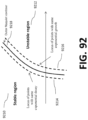
- Antennas as Resonators Some resonator applications are found within antennas, where the antenna circuit is designed to both tune the antenna to a specific frequency band and provide impedance matching, generally to a common reference impedance of 50 ⁇ .
- Antenna impedance matching especially for electrically small antennas (ESA) in RF applications, has been generally accomplished by use of lumped impedance matching components that provide a fixed antenna impedance.
- ESA antennas are commonly, but not exclusively, half-wavelength dipole or even quarter wave monopole antennas that must be designed for a specific application frequency or frequency range.
- SAW/BAW Resonators Other high-performance resonator applications are in the domain of Surface Acoustic Wave (SAW) filters and related Bulk Acoustic Wave (BAW) filters. SAW and BAW RF filters provide very narrow bandwidth (high Q) filtering for communication applications below approximately 6 GHz carrier frequency. Because of the technology deployed, these SAW/BAW devices are subject to thermal variations and aging effects that substantially reduce the filtering effectiveness. Various technology overlays are used in the manufacturing process to either mitigate or eliminate this thermal effect - both at an increased unit price.
- SAW Surface Acoustic Wave
- BAW Bulk Acoustic Wave
- GB 2 478 585 A describes an RF amplifier which is linearised by RF feedback.
- the centre frequency Q of a resonator in the loop filter is adjusted by a control loop so that the resonator centre frequency follows the frequency of the input RF signal.
- the Q of the resonator which is enhanced by local positive feedback, is similarly optimised by a control loop.
- the low Q factor of integrated circuit resonators can be enhanced.
- WO 2015/176041 A1 describes a resonator in which active feedback is used with two electrodes of a four-electrode capacitive-gap transduced wine-glass disk resonator to enable boosting of an intrinsic resonator Q and to allow independent control of insertion loss across the two other electrodes.
- Two such Q-boosted resonators configured as parallel micromechanical filters may achieve a 0.001% bandwidth passband centered around 61 MHz with 2.7 dB of insertion loss, boosting the intrinsic resonator Q from 57,000, to an active Q of 670,000.
- the split capacitive coupling electrode design removes amplifier feedback from the signal path, allowing independent control of input-output coupling, Q, and frequency.
- Controllable resonator Q allows creation of narrow channel-select filters with low insertion losses, and allows increased dynamic range of a communication front-end without the need for a variable gain low noise amplifier.
- EP 1 675 263 A1 describes a method and an apparatus for controlling a Q-factor for a filter.
- the method comprises stabilizing an active feedback to provide a variable feedback in a filter, varying the active feedback based on an input signal to the filter, and producing a desired Q-factor for the filter at a first frequency band, in response to the variable feedback.
- the method further comprises reconfiguring a center frequency and a bandwidth of the filter based on a channel bandwidth of the input signal to the filter to adjust the Q-factor for the filter in response to a second frequency band different than the first frequency band.
- the Q-factor for the filter such as a flexible or reconfigurable filter, may be controlled across a multiplicity of frequency band signals.
- a common signal path may be provided for the multiplicity of frequency band signals within a frequency agile radio of a base station by tuning the radio based on a variable feedback through realization of a negative parallel resistance (FDNR).
- FDNR negative parallel resistance
- tuneability of the Q-factor may provide frequency agile radios that include flexible or reconfigurable filters in a base station to serve different frequency bands without changing hardware.
- a second order ATL would include two such resonators that have two dominant pole pairs, an example being a cascade of two coupled LC tank resonators.
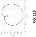
- FIG. 29 shows the frequency response of an example ATL1 after tuning
- FIG. 30 shows the frequency response of an example ATL3 after tuning
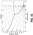
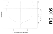
- FIG. 31 is the root locus diagram of the example ATL3 shown in FIG. 30 .
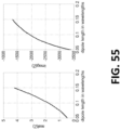
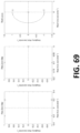
- the fundamental operating principle of the ATL which offers control of bandpass characteristics, is shown in FIG. 2 , where the wide dashed trace 602 is the resonator frequency response at an initial setting.
- the narrow dashed trace 604 is the sharper frequency response of the closed loop filter set for a narrower bandwidth (higher Q) at the initial frequency setting. Assume that the resonator is now tuned upward in frequency to the wide solid trace 606 as indicated by the black arrow 610.
- the narrow solid trace 608 is the closed loop response that results at the new resonator response frequency.
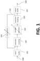
- the circuits are, for convenience, typically depicted in the style of FIG. 1 , which shows an arrangement having a main path 508 and a feedback path 510, and with the gain block 504 (which may also be referred to as a scaling block and which may have both positive or negative values) on the feedback path 510.
- the gain block 504 which may also be referred to as a scaling block and which may have both positive or negative values
- the circuit is more appropriately considered as a loop with appropriate input and output couplings, where the loop is formed from what would otherwise be the main path 508 and the feedback path 510, and the elements are connected in series within the loop. As a loop, the order of the components in the loop may be changed while still being able to provide the desired resonance characteristics.
- FIG. 3 a visual definition of an elemental resonator having s-plane poles is shown.
- the resonator block 1301 is shown in FIG. 3 .
- Resonator 1301 is represented by two poles in the S-plane as is also shown in the diagram on the right of FIG. 3 .
- the two poles are represented by ⁇ x'.
- Resonator 1301 incorporates a feedback loop across a resonator element 1401 as shown in FIG. 4 , which makes Q control possible.
- FIG. 4 is a block diagram showing a first order variable filter ATL-1, having an input 410, an output 412, and a resonator element 1301 having a combiner 1404, a resonator 1401, and a gain or scaling block 802.
- resonator block 1401 connected in a signal loop with gain or scaling block 802 as shown in FIG. 4 is the basic ATL resonator element 1301 that has two control inputs 1302 and 1304: one for changing the frequency (1302), and the other for changing the Q (1304).
- the resonator may be implemented either as a resonator element, such as a LC tank circuit, or as a Second Order Section (SOS) filter element.
- SOS Second Order Section
- FIG. 8 a block diagram of a second order variable filter ATL-2 is shown, having input 810, combiner 1404, resonators 1301, gain buffers 102, gain block 812, and output 814.
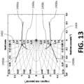
- FIG. 9 shows a root locus of the second order variable filter of FIG. 8 , with open loop roots indicated by ⁇ x' and two poles located at 1902 and two conjugate poles at 1904 for this dual SOS resonator configuration.
- the dominant root trajectories 1906b and 1908b move toward the j ⁇ axis as the closed loop gain G is increased, while the other set of trajectories 1906a and 1908a move away from the j ⁇ axis.
- the ATL will include a feedback loop comprising a desired number of resonators and a scaling block.
- Each ATL may be connected in parallel or in series with other ATL elements, or other circuit elements, and may have an additional Level Two feedback loop that comprises multiple ATL.
- Level Two feedback is intended to refer to a feedback or circuit loop that provides a feedback path around multiple ATLn elements in series. This may also include what could otherwise be referred to as a level three or level four feedback.
- the resonant frequency of R 1401 may be varied with some component included in the resonator circuit. Typically, this may be accomplished using a varactor diode, or a variable dielectric capacitor may be used for a variable capacitance, in which case the ⁇ f control' in FIG. 3 would be an analog bias voltage.
- Other variants that allow the resonant frequency to be varied are well known, such as a discrete capacitance that is switched in or out of the circuit and hence ⁇ f control' may be a digital signal.
- a MEMS variable capacitor or a MEMS variable inductor could be used where ⁇ f control' is a bias control voltage or current signal applied to the MEMS device.
- the variable capacitance or inductance may also be realized by mechanical tuning of a component.
- R 1401 could be a microwave resonance cavity in which one or more dimensions of the cavity are mechanically adjustable by some mechanism supplying ⁇ f control'.
- the 'Q control' 1304 in FIG. 3 above may comprise a control device associated with the resonator that controls the component Q of the capacitance or the inductance or resonant cavity. If the Q control increases the component Q, this is referred to herein as Q-enhancement. If the Q control decreases the component Q of the resonant cavity, this is referred to herein as Q-spoiling.
- Q-enhancement is equivalent to decreasing D, thus moving the resonant pole of R closer to the j ⁇ axis of the S-plane.
- Q-spoiling is equivalent to increasing D, thus moving the resonant pole of R further from the j ⁇ axis hence increasing D. It has been found that Q-enhancement and Q-spoiling may be used selectively to move a resonant pole towards or away from the j ⁇ axis to synthesize an arbitrary multi-pole filter function (plurality of R's).
- Scaling blocks 802, as in FIG. 4 are provided in order to enable better control over the feedback response.
- the gain factor for each scaling block 802 is variable and comprises a gain that includes both positive and negative gain values. For example, if the gain of the scaling block 802 is greater than zero, there results Q-enhancement. If the gain of the scaling block 802 is less than zero, there results Q-spoiling.
- Q-spoiling may be alternately implemented within the resonator element itself by inserting an FET circuit across the resonator element that increases the loss of the resonator. In this manner, the scaling block 802 need only have positive gain.
- each loop or secondary loop in an ATLn element there will be an additional scaling block for each loop or secondary loop in an ATLn element as discussed below.
- ATL3 circuit element see FIG. 20 for reference
- each scaling block will be capable of enabling Q-enhancement resonators and Q-spoiling resonators independently.
- the resonator may be a Q-enhanced resonator, which uses an amplifier that only allows for Q-enhancement.
- the Q-enhanced resonator would still be nested within the feedback loop of the ATLn element comprising a scaling block to override the Q-enhancement and provide a desired Q-spoiled performance as required.
- the resonator may be any type of frequency tunable resonator comprising, but not limited to, a varactor diode, a switched discrete capacitor, a variable dielectric capacitor, a variable capacitor, such as a MEMS variable capacitor, a fixed inductor, a variable inductor, such as a MEMS variable inductor, or a mechanically adjustable resonator.
- ATL1 a first order of the ATL circuit, denoted ATL1, which comprises a single resonator component 1401, a single gain or scaling block 802, and a combiner 1404 for closing the feedback loop as depicted in FIG. 4 .
- the ATL1 is the core module of the ATL variable filter in that all variants of the ATL variable filter use various combinations of this ATL1 core module.
- ATL1 core module may be described in a simplified way if the center frequency control of the ATL1 core module is omitted. This provides an intuitive method of understanding the ATLn variants, all based on this ATL1 core module.
- resonator 1301 may be a second order bandpass filter with a transfer function of: 1 s 2 + 2 D ⁇ o s + ⁇ o 2 with coefficients evaluated based on D and ⁇ o .
- the gain G 802 is variable and controls the closed loop Q. Note that at resonance the phase shift through the resonator 1401 is ideally 0 degrees.
- phase shift will not be zero in general due to parasitics and transport effects, but these may be ignored in this evaluation: the implemented circuit may require a phase shifting element associated with G 802 that will compensate for any parasitic and transport phase effects, as is discussed later. To vary the frequency, it is necessary to change ⁇ o of the resonator in the ATL1, but this is ignored in this section.
- the first order ATL1 core module has a resonator of first order. What is referred to in "order” is the number of Second Order Sections (SOS) used that make up the overall resonator.
- SOS Second Order Sections
- An SOS transfer function refers to a Laplace function of frequency variables that are second order in the denominator.
- H SOS s as s 2 + 2 D ⁇ o s + ⁇ o 2
- ⁇ o the resonance frequency in radians per second
- D is the damping coefficient
- a is a real constant.
- ⁇ f n ,Q ⁇ may then be used interchangeably with ⁇ ⁇ n , D ⁇ .
- the root locus is a standard method of determining the poles of a closed loop system given a variable loop gain.
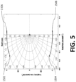
- the outcome of the root locus calculation in the present context is the trajectory of these closed loop poles as they change with variations in the loop gain G as shown in FIG. 5 for example.
- FIG. 5 is a root locus of the first order variable filter shown in FIG. 4 .
- the poles are shown at 1502 and 1504, while the root locus of the poles are shown at lines 1504 and 1508.
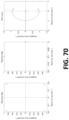
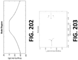
- FIG. 6 is a bode plot of the first order variable filter shown in FIG. 4 .
- FIG. 6 shows a plot of the magnitude 612 and phase 614 changes with frequency. Note that the phase change with frequency is rather gradual around resonance due to the high damping factor (low Q) assumed in this example.
- the ATL1 In this unstable region of operation the ATL1 is not usable and root trajectories cease to be meaningful. Hence we only need to plot over the range of G in which the closed loop poles remain in the left hand plane (LHP).
- LHP left hand plane
- the radial dotted lines in the root graph indicate the damping value of D.
- variable Q for the SOS resonator
- ⁇ Q-spoiler' is implemented via a variable resistive element in the SOS such as a variable FET circuit or PIN diode that can increase the loss of the SOS, thus reducing Q.
- the variable resistor reduces (spoils) the Q such that the poles of the SOS are further from the j ⁇ axis into the LHP as mentioned above. This is a degree of freedom (DOF) that allows for higher attenuation of outliers than if an SOS with a fixed lower Q was implemented.
- DOF degree of freedom
- the Q-spoiler is implemented with a FET 1702 operating in the triode region in parallel with a resonator 1701 and controlled by a Q-spoiler control voltage 1704 to provide an equivalent variable resistor function.
- the FET 1702 could be implemented with a PIN diode. It will be understood that these design options may be incorporated into any of the adaptive filter circuits described herein.
- the single resonator 2702 is a fixed resonator circuit with a feedback gain 2704.
- G may be negative for Q-spoiling or positive for Q-enhancement
- gain block 2704 is shown as a two-port gain block that it may be arranged as a one port gain block with either negative or positive resistance. Negative resistance would result in G being equivalently greater than zero and provide Q-enhancement. Positive resistance, on the other hand, is equivalent to a negative G providing Q-spoiling.
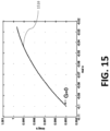
- the root locus of the positive frequency closed loop pole for positive G 1510 is shown in FIG. 15 . This corresponds to the Q-enhancement case where the close loop pole moves towards the jco axis.
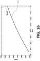
- the root locus for negative G 1610 is shown in FIG. 16 . This corresponds to the Q-spoiling where the close loop pole moves away from the j ⁇ axis.
- the resonator R comprises a means to vary the resonance frequency of the ATL1.
- the time required to tune from one frequency to the next is approximately equal to the reciprocal of the bandwidth of the ATL1.
- FIG. 10 The topology of the third order variable filter ATL3 is shown in FIG. 10 , comprising three cascaded ATL1 SOS resonators, each of which includes a feedback loop 1010, a method for changing the center frequency of the resonator, and a method for changing the Q of the resonator.
- unit gain buffers 102 are placed between all of the resonators 1301 for isolation, and a combiner 1404 to close the feedback loop.
- FIG. 10 also shows input 1012, output 1014, and gain block 1016. It is important to note the fundamental ability to individually control both the center frequency and gain of the individual resonators in this and other ATLn configurations. Initially, we shall set the center frequency of each resonator to be the same and will discuss the ATL3 with different center frequencies later.
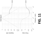
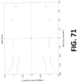
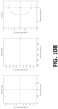
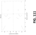
- FIG. 11 shows the Bode plot of the triple resonator, each with the same center frequency, which the out of band open loop attenuation of the triple resonator is seen to be 60 dB per decade in frequency which is of significance as it is based on low Q resonators.
- FIG. 11 shows the plot of the magnitude 1110 and phase 1112.
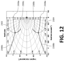
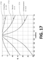
- the root locus is interesting in that there are three root trajectories 2306a/b/c and 2308a/b/c emanating from each triple of open loop poles 2302 and 2304 marked again by the 'x', although image scaling makes the three individual roots impossible to differentiate.
- one of the root trajectories 2306a/2308a follows the contour exactly as before, while the other root 2306b/2308b goes further into the left-hand plane (LHP) and does not influence the circuit.
- the third pole trajectories 2306c/2308c start to move toward the j ⁇ axis. This potentially gives rise to a spurious mode that is at much lower frequency than the intended passband.
- this potentially troublesome pole is still far from the j ⁇ axis and causes a negligible spurious response in a practical implementation.
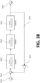
- ATL3 Topology 2 (ATL3 T-2), seen in FIG. 38 , considers adding a single feedback loop 3810 around the three series ATL1 core modules, connecting the output of the final ATL1 to the input of the first ATL1. As shown, FIG. 38 has input 3812, combiner 3814, resonators 3816, output 3818, and gain block 3820. ATL3 T-2, however, has no feedback loops within the individual ATL1 core modules. As will be pointed out, this topology results in an under-specified design situation, meaning that the performance of this topology might not meet stringent design performance criteria. But there are possible advantages, driven as always by design tradeoffs.
- ATL3 Topology 3 (ATL3 T-3), seen in FIG. 20 , where a Level Two feedback path 110a is wrapped around the three ATL1 core modules, with the individual ATL1 core modules containing independent Q and center frequency control.
- FIG. 20 shows resonators 1301, buffers 102, and feedback loops 110, in addition to level two feedback path 110a.
- the pole movement in the S-plane will be as illustrated in the right hand side of FIG. 21 .
- the arrows 3602 in FIG. 21 are for negative feedback (Q-spoiling) and the arrows 3604 are for positive feedback (Q-enhancement).
- the pole movement of this ATL3 T-3 in the S-plane as illustrated in the right-hand side of FIG. 21 . Note that only the dominant poles move toward or away from the j ⁇ axis.
- the pole control of the tunable analog ATL3 enables a variety of complex filter responses with control of the passband for the variable bandwidth filter.
- the nature of the dominant pole that arises with this ATL3 topology leads one to consider this ATL3 topology as a single pole filter implementation, a fact that will be amplified upon later.
- any required phase control for the ATL variable filter may be implemented via slight detuning of the ATL1 core modules that comprise the ATL3. In this manner, no separate phase control element is necessary, simplifying design and fabrication.
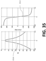
- the frequency (3510) and phase (3512) response is presented in FIG. 35 .
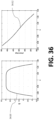
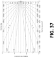
- This Butterworth pole-zero map is shown in FIG. 37 .
- the phase shift is 0 degrees at the center frequency
- flanking poles are about half the distance to the j ⁇ axis as the center pole. This implies that these passive Butterworth poles have twice the Q of the center pole.
- the arrangement of three ATL1 core modules can realize three resonant poles as discussed.
- this may also be used to provide similar results as a classic passive third order Chebyshev type bandpass filter.
- an equivalent Chebyshev scheme is shown using three ATL1 core modules, where the resonators 1401 each have a feedback path 110 with a scaling block (not shown) and are separated by buffers 102.
- the poles of the three ATL1 core modules are generated as described above and may be set arbitrarily close to the j ⁇ axis.
- a simpler bandwidth control is that of implementing the Level Two feedback loop 110a as shown in FIG. 20 .
- the feedback around each ATL1 core module is driven from a common control source (not shown), and each ATL1 core module feedback loop has a gain block (not shown), as described above.
- the first level control for the ATL1 core modules moves the three poles in unison towards or away from the j ⁇ axis, as shown diagrammatically in the left side of FIG. 21 .
- the outer Level Two control loop 110a that is around the three individual ATL1 core modules also has a gain block (not shown).
- Level Two control we can spread the outer flanking poles and cause the center dominant pole to move either toward or away from the jw axis, as shown diagrammatically in the right side of FIG. 21 . It is important to note that the three poles can move in opposite directions. This important result enables controlling the bandwidth of the filter with relative ease, while maintaining a similar frequency response.
- each of these three ATL1 core module resonators are with feedback loops such that there are 3 cascaded individual ATL1 core modules.
- the root locus is shown in FIG. 22 .
- the 'x' 3702a/b/c designate the positions of the poles with feedback gain of 0.
- the gain is positive for right excursions 3704a/b/c towards the j ⁇ axis (Q-enhancement) and negative for excursions 3706a/b/c to the left (Q-spoiling).
- Q-enhancement negative resistance amplification
- the range of the feedback gain for each root trajectory is -1 ⁇ G ⁇ 0.9.
- FIG. 26 shows how the preferred ATL3 topology Level Two feedback may be used to control the bandwidth of the filter. Positive Level Two feedback narrows the filter bandwidth and negative Level Two feedback broadens it. Only a very small amount of preferred ATL3 topology Level Two feedback is needed for this control.
- the Level Two feedback was 0 (line 2610), -0.002 (line 2612), and +0.002 (line 2614), as indicated.
- the preferred ATL3 topology Level Two feedback control of FIG. 20 allows for an effective means of bandwidth control that may be practically implemented.
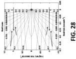
- FIG. 28 shows the zero degree root locus of this configuration, which is very similar to that shown in FIG. 12 where each of the three SOS resonators has the same center frequency.
- the ATL1 core module may provide good band pass filtering performance for many applications.
- the ATL1 core module provides the basic frequency tuning and Q adjustment of the ATL concept.
- the ATL2 and ATL3 filters may give more flexibility for tailoring to an application.
- the ATL3 will provide the best rejection of the out of band signals for typically encountered closed loop Q values.
- an adjustable phase shifter may also be used to provide some circuit control.
- adjustable phase shifters that may be used in the context of ATL-based circuitry.
- Other types of phase shift elements that provide an adequate level of performance may also be used.
- the ATL3 is comprised of three ATL1 core modules, it is important to examine the phase control of this ATL1 core module. It has been found that the closed loop passband of the ATL1 core module forms around the range of frequency where the open loop phase shift is a multiple of 360 degrees. As it is desired to have only a single passband, the passband of the resonator may be arranged to coincide with the frequency of a multiple of 360 degrees phase shift. If the resonator peak frequency is misaligned, then the closed loop response peak will still coincide with the frequency at which a multiple of 360 degrees is achieved, although the passband may be distorted.
- the phase control may in principle be any circuit that can alter the signal phase shift at the resonance frequency. It does not have to provide a constant phase shift across a band of frequencies, nor does it have to provide a constant delay across a band of frequencies.
- the required characteristics of the phase shift function are:
- phase shift provided must be relatively smooth throughout the closed loop Q-dependent bandwidth of the ATL1;
- FIG. 39 shows ATL1 band 3914.
- the magnitude of the transfer function through the phase shifter should not vary drastically over the Q-dependent bandwidth of the ATL1.
- a variable phase shift may be introduced by starting with a variable delay line that is made up of a uniform sequence of varactor diodes along a transmission line. By varying the varactor voltage, the group delay may be varied, and by changing the group delay, the phase may be shifted.
- variable phase shifters, resonators, delay lines and quadrature modulators may be considered as circuits arranged and optimized to provide a variable delay over a range of frequencies.
- variable resonator and variable phase shifter By generalizing the variable resonator and variable phase shifter and recognizing that they are functionally similar in the context of application to the ATLn, it is possible to use a plurality of sub-circuits in the loop, where each sub-circuit may be controlled to give a desired delay and amplitude response that may be controlled by a plurality of control voltages.
- the ATL1 core module is a single variable resonator sub-circuit. Potentially, with careful design, the phase shift may be a multiple of 360 degrees at a desired frequency within the passband of the resonator. Shifting the resonant frequency equivalently shifts the phase. The ATL1 response peak will occur where the loop phase shift is a multiple of 360 degrees.
- the limitation of the ATL1 with only a variable resonator is that the phase shift adjustment of the resonator is limited. Hence if the loop has a large phase error, then there is not enough range with the single resonator, requiring a variable and fixed phase shifter to be added. However, based on the above discussion of general phase shift control considerations, this is equivalent to stringing a number of delay controllable sub-circuits in series.
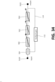
- variable phase shifter has a flatter frequency response in terms of magnitude and may therefore be used over a larger frequency range, but this comes at a cost of adding more components, some of which are difficult to integrate into a chip. If three resonators are added, this is equivalent to a special case architecture of the ATL3. This is shown in FIG. 34 , with input 3410, output 3412, three variable resonators 502, which may be ATL1 elements, a feedback path 110, a coupler 104, and a gain element 112, which may be controllable.
- FIG. 40 shows an idealized model of ATL1 with two implementations, having resonator 4010 and scaling block 4012 in different positions.
- D s 1 + GF s
- XR(s) is the open loop transfer function
- G is the loop gain.
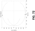
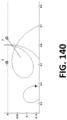
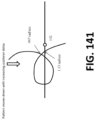
- a typical Nyquist stability plot is shown in FIG. 41 where the points of the locus crossing the positive portion of the real axis are coincident with the open loop phase being a multiple of 360 degrees.
- the frequency response may be determined (relative to the closed loop denominator) as the inverse of the phasor shown between the real axis point of 1/G and the open loop transfer function F(jw).
- F(jw) the open loop transfer function
- a pure phase shift is not possible to implement as the circuit becomes infinitely complex. We can only implement this approximately over a narrow frequency range.
- FIG. 42 wherein we show the Nyquist plot of a resonator over a small frequency range as curve 4210.
- the resonance response decreases as the phasor length from 1/G to the resonance point increases.
- G increases, the ATL1 will peak at the point A instead of the resonance point.
- the peak closed loop response of the ATL1 will shift in frequency, which is not desirable.
- the peak response for finite Q is not necessarily the frequency coincident with an open loop phase shift that is a multiple of 360 degrees.
- the loop phase will asymptotically approach a multiple of 360 degrees.
- Rotating the open loop transfer function such that its peak is along the real axis can set the phase shift correctly.
- the frequency will not shift as the Q is enhanced or spoiled.
- phase shifter function that is required is not a constant but rather a smooth function over the range of the closed loop narrowband response of the ATL1.
- phase shifter An issue with this phase shifter is that as the varactor capacitance C increases, so does the loss of the circuit. Also, the range of phase shift is not sufficient. To solve this multiple RC segments may be used. This solves both problems but requires higher complexity.
- the desired chip implementable phase shifter is a type of resonant delay circuit that provides a smoothly varying delay over a relatively small bandwidth.
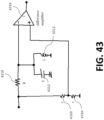
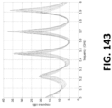
- Such a phase shifter is the all-pass circuit shown in FIG. 43 , having resistors 4310, capacitor 4312, inductor 4314, and difference amplifier 4316.
- R can be implemented with a combination of a FET and capacitor implemented as a varactor diode, which allows for controlling the position of the poles and zeros.
- phase curve By changing the all-pass frequency ⁇ p , the phase curve can be shifted left or right, providing phase control for a given passband.
- the constant amplitude response of FIG. 45 is an advantage in that the phase can be changed without changes to the loop gain. Also, note that this phase shifter has a range approaching 360 degrees.
- the ATLn is a bandpass filter comprised of a series of "n" each ATL1 core modules, in one of three possible topologies as discussed above.
- Each of the ATL1 modules is independent in performance and may be adjusted for both the center frequency and the Q value of the resonator and may include an amplifier in a feedback loop around the resonator.
- Each ATL1 is isolated from the other ATL1 modules using circuit coupling buffers, which ideally introduce zero phase shifts.
- the open loop phase shift of the ATL1 resonator should be zero degrees at the center frequency of the passband, and highly linear throughout the passband. This can be achieved with an ideal resonator without any parasitics.
- the phase of a signal may be affected by many different factors as it passes through a circuit, some of which include stray component capacitances and inductances that may be referred to as "parasitics”.
- parasitics associated with the ATL1 resonator (or resonators as in the ATLn), and there is phase shift associated with the buffer amplifiers. In the ATLn, where n ⁇ 2, the excess phase shift may exceed 360 degrees. Certainly excess phase needs to be considered.
- phase shifter may be adequate for an ATLn circuit that is implemented on a chip, where parasitics are generally minimal, well modeled and understood, and where the ATLn circuit is intended to be used over a modest frequency tuning range. In other circumstances, such as when the ATLn is implemented as discrete components or with surface mount architectures, it may be necessary to incorporate a variable phase shifter to correct the phase of a signal passing through the circuit.
- phase shifter used will depend on the actual implementation of the circuit.
- Various types of phase shifters are known in the art, and a person of ordinary skill may incorporate a suitable phase shifter into an ATLn as needed.
- ATLn topologies discussion above we showed that it is not necessary to implement a separate phase shifter element, as it is possible to easily control net loop phase error by minor frequency adjustments to the ATL1 core modules that comprise the ATLn. This important result applies to all ATLn variants of the ATL variable filter for n > 1.
- variable gain block can be realized with a differential amplifier and a FET to control the source current and hence the gain of the differential amplifier.
- One of the two outputs of the differential amplifier can be selected with a switch.
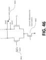
- FIG. 46 A simplified schematic of the variable gain with a polarization selectable output 4610 is shown in FIG. 46 , having input 4612 and current adjustment for gain control 4614.
- This gain polarization switching circuit is a simple integration of a differential amplifier with a control for the gain based on adjusting the current through the differential FET pair via the bottom FET shown. Selection of the outputs from the two differential outputs provides the polarity selection.
- An alternative might be to use a full Gilbert cell integration. A Gilbert cell is more elaborate than what is required for the ATL3 implementation. However, there may be other considerations not considered here that may deem the Gilbert cell as a better choice.
- the closed loop center frequency will be at the correct frequency when phase shift at that frequency is a multiple of 360 degrees.
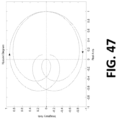
- FIG. 47 A typical Nyquist plot based on this ATL1 phase shift control implementation is shown in FIG. 47 .
- a parasitic delay resulted in a phase shift of 0.6 radians.
- the all-pass network is based on a resonator
- the all-pass phase shifter provides constant magnitude which is not needed for phase shifting.
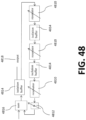
- FIG. 48 shows a block diagram of the ATL3 with three cascaded resonators 4810, with a variable gain block 4812, a gain polarity selection buffers 4814, sum 4816, and output 4818.
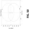
- isolated resonators 4910 are not necessary and we can group the three required resonators into a composite bandpass filter with three poles as shown in FIG. 49 .
- gain block 4912 Also shown in FIG. 49 are gain block 4912, sum 4914, isolation buffer 4916, input at 4918, and output at 4920.
- the resonators only need to be detuned by about 5 % each to accommodate this worst case parasitic phase shift. Also, as described before, if the parasitic phase shift is increased beyond 1.5 radians then the other polarization output of the variable gain block is used.
- control voltages may be set that adapt the performance of the ATLn for the target application, based on the following principles:
- the signal phase shifter implemented with varactor diodes, may require additional control voltages.
- Signal phase shifting arises from the delay and phase shift of components and interconnections for implementations at either a) bulk component level; b) component surface mount level; or c) integrated chip level. It is necessary to compensate these phase changes in the feedback loop(s) with a phase shifter that can properly restore the overall phase shift of the loop.
- LUT Look Up Table
- the basic ATL1 calibration data is resident in the LUTs.
- the ATLn there will be 3n calibration LUT, each LUT containing
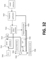
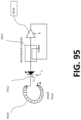
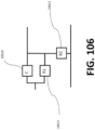
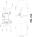
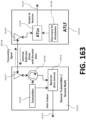
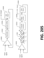
- FIG. 32 presents a circuit that has processing built in for the purpose of calibrating and stabilizing the response of an ATL1 block 7502.
- FIG. 32 shows ATL-1 7502, power detector 7512, ADC 7514, frequency down converter 7510, frequency counter 7509, temperature sensors 7508, ⁇ P 7504, LUT 7516, control PWM (f, Q) 7506, frequency synthesizer 7507, and crystal reference 7505.
- the microprocessor 7504 generally a system asset, adjusts the control for the frequency and Q of the ATL1 7502 through a digital to analog converter (DAC) implemented as a pulse width modulation (PWM) circuit 7506, and based on readings from a temperature sensor 7508.
- the microprocessor drives the ATL1 7502 to the start to self-oscillation.
- the frequency of this self-oscillation is down converted in block 7510 by a frequency synthesizer signal generated by a crystal reference 7505 and a frequency synthesizer 7507 that is set also by the microprocessor 7504.
- a frequency counter 7509 or other measurement means determines the frequency of the down-converted signal.
- the resonant frequency of the ATL1 core module may be determined.
- a power detector 7512 and analog to digital converter (ADC) block 7514 that can estimate the rate of increase of the self-oscillation signal at the output of the ATL1 7502.
- the microprocessor 7504 estimates this exponential rise of power and from this determines where the closed loop pole of the ATL1 7502 is. Presently it will be just to the right of the jw axis. If the Q-enhancement is decreased slightly then the self-oscillation will continue at the same frequency to a high accuracy but will begin to decay exponentially. Now the pole is on the left hand side of the jw axis.
- this exponential decay may be measured, and the operating point measured.
- the mapping of the ATL1 7502 to the f and Q control signals may be completed.
- This calibration may be done based on circuitry on chip that requires no additional off chip components except for the crystal reference source. During operation, calibration breaks may be made such that the LUT 7516 is continuously updated. In the case of a wireless sensor, the transmitter and receiver functions are separated by epochs of inactivity in which the calibration processing may be done.
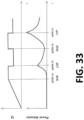
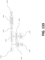
- FIG. 33 shows an example of the Q control of the ATL1 alternated between higher and lower levels that alternately places the closed loop pole of the ATL1 in the right hand and left hand planes.
- the resulting exponential rise and decay is easily measured by the power detector with numerical analysis done on the microprocessor.
- the applied Q control voltage may be mapped to a specific pole position. This is stored in the LUT such that when a pole position is required for the filtering operations of the ATL1 then the LUT may be interpolated and the ⁇ f,Q ⁇ control voltages set.
- Either the times of t 1 and t 2 may be set and the voltages x 1 and x 2 measured, or else fixed thresholds may be set at x 1 and x 2 , and the time difference of t 2 - t 1 may be measured. Either approach is straight forward.
- the above calibration procedure is repeated for each ATL1 core module within the ATLn.
- the ATLn may be designed to relatively easily broaden the bandwidth.
- a small amount of Level Two feedback gain G around the 3 Rs of an ATL3 is a simple and robust way to change the passband from something representing a single pole passband response to a broader response similar to a third order Chebyshev filter.
- An application of this control concept may be in a wireless sensor, and may provide the following aspects:
- the envelope of the self-oscillation of the ATL1 may be used as a probe signal to estimate the real part of the pole location.
- the imaginary component is determined by the frequency of self-oscillation.
- the self-oscillation may be measured based on comparison with a crystal locked synthesizer frequency.
- the three resonators (R) of the ATL3 may also be used directly.
- the ATL1 allows for calibration to be continuous and in parallel with the operation of the ATL3 which is then dedicated for the actual signal processing.
- the measurements of the ATL1 pole location as a function of the control voltages and perhaps chip temperature is stored in a LUT.
- the values of the LUT are interpolated when the ATL3 is to be configured.
- the ATL1 calibration is stable over time, varying primarily based on ambient temperature, it may not be sufficient for precision filtering operation for applications that require high Q narrow bandwidth operation where the poles are very close to the j ⁇ axis.
- the ATL passband is affected by the load match at the input and output terminals.
- This relative frequency accuracy is typically provided by a crystal reference that is available in all communications devices. In applications where the highest precision is not needed, or when an external crystal reference is not available, high performance is still achievable.
- a factory calibration may not be sufficient for this level of highest precision, such that initialization calibration, and possibly run time calibration, may be necessary. What is more, in narrow bandwidth operations, the Q enhancement factor may be large and therefore the loop gain has to be set very precisely. If the loop gain is changed by as little as 100 ppm in high precision applications where narrow bandwidth linear filtering mode is desired, the ATLn can push the closed loop poles over the jw axis into the right hand plane (RHP) resulting either in a) self oscillation; or b) transitioning into an injection locking. Hence precise calibration of the loop gain is also required. To address these calibration issues, two calibration modes, discussed in detail below, are envisioned.
- ATL1 self-calibration at any system implementation - be it discrete component level, surface mount level, or as an integrated chip - is based on measurements of the ATL1 passband as a function of the ⁇ f,g,p ⁇ control voltages.
- the ATL1 can go into this self-calibration mode every time it is requested to do so by an upper application layer that either a) repopulates the LUTs or b) can do a weighting of the previous and current measurements.
- These ATL1 measurements will be done with the input and the output loads of the circuit in place such that any deviation due to port impedance mismatch is accounted for.
- a temperature sensor is also provided with the ATL1 circuit such that the sensitivity due to temperature changes may be calculated. Note that this is done over multiple calibration runs and by analysis of the drift during run-time. Note also that this in-situ calibration also accounts for the voltage regulation errors and any offsets in DAC voltages for the ⁇ f,g,p ⁇ controls.
- Initialization is only required when the initial parameters for operating frequency and bandwidth (Q) are established. If multiple operational frequencies are required, as in a frequency hopping application, initialization is required at each operational frequency. Operation of the ATL1, and by extension the ATLn, has proven to be stable over time and hence initialization is not routinely performed.
- the sole parameter that affects operational calibration is the ambient temperature of operation, which is the subject of run time calibration.
- each of the ATL1 core modules much be separately initialized and their respective LUTs established.
- Run time calibration is application specific.
- the ⁇ f,g,p ⁇ control parameters may be set by dithering or other optimization strategies to maximize the quality of the ATL1 filtering. Corrections to the LUTs may be noted as deviations from this optimization process. Hence the LUTs are continuously optimized. Algorithms for long term annealing of the LUT may be customized to the specific applications.
- the frequency passband response is measured relative to a crystal-based reference oscillator or other frequency reference source.
- ATL1 initialization self-calibration and ATL1 run time calibration.
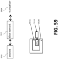
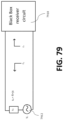
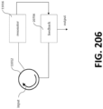
- This structure is dependent upon the physical implementation of the ATL1 core module, be it at discrete component level, surface mount level, or an integrated chip implementation. While any application could be considered (an ATL3 or the ATLF for example), in order to focus initially on the concepts of self-calibration and stability control only, the ATL1 core module is implemented within an overall wireless sensor transceiver system consisting of a minimal four components, a block diagram of which is shown in FIG.
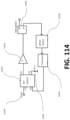
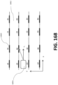
- ATL1a and ATL1b show antenna 14610, switch array 14612, ATLa 14614, ATLb 14616, down/up conversion and ADC/DAC sampling 14618, ATL control 14620, baseband processing 14622, LO/ADC clock synthesizer 14624, power conditioning 14626, transceiver chip 14628, clock crystal 14630, and power source 14632.
- ATL1a and ATL1b we show a pair of standard ATL1 core modules labeled as ATL1a and ATL1b. They are chip implementations of the ATL1 and considered to be identical and uncalibrated. But the following calibration process would be the same at discrete component level and surface mount implementations of FIG. 146 . Chip level implementation, however, likely provides the highest level of precision.
- the antenna is connected to an operational mode switch matrix that enables different configurations of the ATL1a and ATL1b for calibration mode, transmit mode, and receive mode.
- the switch will have some insertion loss and will contribute to the receiver noise figure (NF).
- NF receiver noise figure
- the baseband processing is used to generate observables from which the ATL1a and ATL1b may be controlled.
- the control is shown as a red line that also affects the switch array.
- the overall goal is to develop a practical means of self-calibration of the ATL1a and ATL1b that is done within the transceiver module outlined in FIG. 146 by itself. That is, the transceiver module as shown in FIG. 146 will be fabricated and inserted into the transceiver system initially uncalibrated. Upon application of power, the transceiver module enters a self-calibration mode wherein it generates a look-up table (LUT) for the control voltages of ATL1a and ATL1b necessary to support a given center frequency and Q. The calibration will be ongoing during operation in various modes. In this way the transceiver chip will self-learn as it is operating.
- LUT look-up table
- the clock crystal sets the reference frequency to be used.
- inexpensive clock crystals are only accurate to within about 100 ppm, it is possible in various scenarios to use an incoming reference signal to determine the frequency offset of the clock crystal, as mentioned above, and store this also in the LUT.
- ATL1 may be operated as a stable oscillator with a tunable frequency, and that this output may be fed onto another ATL1 to determine its frequency characteristics.
- ATL1a becomes a voltage controlled oscillator (VCO) that feeds into ATL1b to determine the bandpass characteristics of ATL1b, and then to use ATL1b as a VCO to feed into ATL1a to in turn determine the bandpass characteristics of ATL1b.
- VCO voltage controlled oscillator
- ATL1a and ATL1b are built on the same chip die, operate at the same temperature and have the same voltage applied to it and age in the same manner, they will be very closely matched in terms of operating characteristics. This helps with the calibration as will be elaborated on later.
- a key innovation is that the chip is a transceiver and therefore has baseband processing that is clocked based on the frequency corrected clock.
- the stability of the clock crystal is therefore effectively mapped into the ATL1a and ATL1b. That is, say that ATL1a is used as a VCO set up to operate at a specific frequency based on control settings. Then it is possible based on the down conversion (based on an LO synthesizer derived from the clock crystal) and ADC sampling (clock also based on the clock crystal) to determine the frequency of the ATL1a relative to the corrected clock crystal frequency.
- the Q of the primary resonator may be considered high relative to the adjustable resonator, where a high Q resonator may be considered to be a factor of 10 greater, or even a factor of 100 greater, than the adjustable resonator.
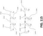
- the basic receive mode (Mode 1 shown in FIG. 147 ), where we have the ATL1a forms the RF filter.
- FIG. 147 shows antenna 14710, ATLa 14712, and down conversion ADC sampling 14714. In this mode the ATL1a will have relatively high Q and also will have a high gain.
- ATL1a and ATL1b are cascaded (Mode 2 shown in FIG. 148 ) where the ATL1a will have a lower Q, broader bandwidth and ATL1b will be narrower bandwidth and higher Q.
- FIG. 148 shows antenna 14810, ATLa 14812, ATLb 14814, and down conversion ADC sampling 14816. The idea is that ATL1a will suppress some of the out of band tones and have better intermodulation performance as it is lower Q. The ATL1b will be narrower bandwidth with a higher Q.
- FIG. 149 shows antenna 14910, ATLa 14912, attenuator 14914, ATLb 14916, and down conversion ADC sampling. If the gain is too high, then it is difficult to ensure that the transceiver chip remains stable. Note that this attenuator is a relatively trivial circuit that may be added in at the output of the ATL1a.
- Mode 3 is the basic transmit mode that works in conjunction with mode 1 for the receive mode.
- FIG. 150 shows antenna 15010, ATLb 1501, and up conversion DAC sampling 15014.
- the switch array would facilitate the switching between the mode 1 and mode 3 for the TDD function.
- FIG. 151 shows ALTb 15110, attenuator 15112, ALTa 15114, and down conversion ADC sampling 15116.
- An attenuated sinusoidal signal then goes into the ATL1a and is down converted and sampled.
- Subsequent processing measures the level and frequency of the signal output of the ATL1a. In this way, the ATL1a bandwidth and center frequency may be tuned.
- Mode 5 shown in FIG. 152 , is the reverse of Mode 4 in that the ATL1a is used as the VCO and fed into the ATL1b that operates as a filter.
- FIG. 152 shows ATLa 15210, attenuator 15212, ATLb 15214, and down conversion ADC sampling 15216.
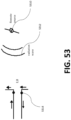
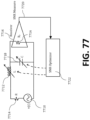
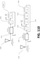
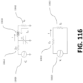
- FIG. 153 shows coupler 15310, resonator 15312, scaling block 15314, and phase shifter 15316.
- control voltages ⁇ f,g,p ⁇ one for the resonator frequency, one for the scaling block setting and the third for the phase shifter control.
- the ATL1b fabrication is sufficiently controlled such that the resonator of ATL1b may be set such that it is approximately in the middle of the tunable band. This implies that we are assuming reasonable fabrication control of the varactor diodes used in the resonators. Also, the resonator for ATL1a is initially set in the middle of the tunable band.
- the gain is increased.
- the ATL1a resonator oscillation condition is met when the loop phase around the ATL1a is a multiple of 360 degrees, and that the loop gain is slightly less than unity.
- the ATL1a phase is then adjusted such that the scaling block is set to the minimum feedback gain to sustain oscillation.
- the difficultly will be in observing the oscillation as the baseband processing has a restricted bandwidth. Hence an initial search over the resonator voltage and the phase is required for ATL1a.
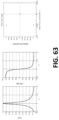
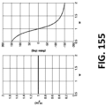
- the frequency response is shown in FIG. 155 . Note that the magnitude response is flat as required of an ideal phase shifter, and that the phase is a decreasing slope with frequency representing a near constant delay over an approximate frequency range of ⁇ 20%. By changing the all-pass center frequency ⁇ p , the phase curve can be shifted left or right providing phase control.
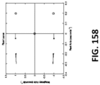
- the zero-degree root locus of the resonator is shown in FIG. 158 , where we additionally show both the poles and zeros of the phase shifter.
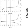
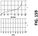
- the new phase plot of the phase shifter now shows a lag of 50° as seen in FIG. 159 .
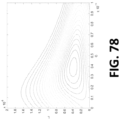
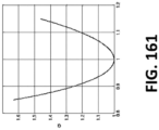
- FIG. 161 shows a plot of the loop gain required to reach the oscillation condition as a function of the phase shifter mismatch. We map this into the equivalent phase shift shown in FIG. 156 .
- ATL1 core module resonance frequency and phase shifter values can be set by increasing G and noting the point where the ATL1 core module begins to oscillate.
- the following procedure is one possible sequence: Set up the switch array to give us Mode 4 shown in FIG. 151 .
- Mode 5 shown in FIG. 152 is switched in, reversing the functions of ATLla and ATL1b. That is ATLlb is now set up for no feedback and hence broad bandwidth.
- the LUT entries for the ATLlb may be used as initial points for the ATLla calibration. In the case where the ATLla and ATLlb are located on the same chip die, and operated under the same conditions (temperature, supply voltage, etc.), the LUT entries for ATLla for should be very close.
- the ATLla is then set up as an oscillator and the calibration table filled, following the procedural steps as above, for the ATL1a.
- the LUT's are now populated with the conditions for the closed loop resonant poles to reach thejw axis for both the ATLla and ATL1b.
- the final step is to interpolate these values into a uniform frequency sampling, which is easily done as the data collected from the initial step is sufficiently dense.
- Mode 4 ( FIG. 151 ) again, but now with the ATLlb as a VCO that can be tuned fairly accurately.
- the precise frequency of the ATLlb will ultimately be determined by the LO down conversion and the digital signal processing (DSP) baseband processing. This determined frequency is 'exact' in the context of the clock crystal.
- DSP digital signal processing
- ATLlb oscillates as a VCO at ⁇ a with the signal passed into ATL1a.
- the phase shifter control and open loop resonator control voltage of ATLla are dithered in a synchronous fashion based on the LUT entry. This causes the passband of the ATLla to be dithered in terms of the center frequency.
- the down conversion, ADC and subsequent processing determines the amplitude variation of the frequency component at ⁇ a . The variation is used to determine the bandwidth of the ATLla with a specific feedback gain. This observation is now an entry into the LUT for ATL1a. Then the feedback gain of ATLla is incremented and the process repeated.
- ATLla is calibrated in this fashion then we can go back to Mode 5 ( FIG. 152 ) and use the ATLla as the VCO and measure the bandwidth of ATLlb for various feedback gain settings.
- variable resonator is an ATL-based circuit that controls an external resonator (XR)
- this circuit design may be referred to as an ATLXR.
- ATLXR As the discussion below will be in terms of an ATL-based circuit used with an external resonator, the term ATLXR will be used as a shorthand reference to a primary resonator that is modified by an adjustable resonator. However, it will be understood that the principles discussed may be expanded to other circuit designs in which other types of resonators are controlled using the ATL-based circuits described herein, which may not be considered external, as well as other suitable types of adjustable resonators.
- the primary resonator may be a fixed resonator or a resonator that is tunable in frequency. However, for practical reasons, the primary resonator is preferably stable over the cycle time of the secondary variable resonator control and response loop such that the external predetermined primary resonant structure appears "quasi-fixed" for system performance purposes.
- This approach may be used to make small adjustments post-production that may increase production yields for high Q and moderate Q filters.
- the yield improvements may amount to adjusting the Q and/or center frequency of the fixed resonant structure.
- the frequency response of the primary resonator may be designed to operate within a predetermined error factor, such as may be specified by the manufacturing specifications.
- the adjustable resonator may then be used to control the primary resonator within this predetermined error factor to cause the closed loop frequency response to approach the ideal frequency response of the primary resonator.
- an external resonator denoted by XR
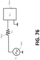
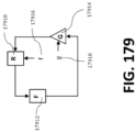
- the XR resonator is connected in a signal loop with active signal amplification gain block g and an additional second variable resonator, denoted by R, as shown in FIG. 179 .
- the variable R resonator 17910 is controllable in terms of resonant frequency by a control f 17916, and may have a low Q, relative to the external resonator F 17912.
- the gain block G 17914 is controllable by g 17918.
- the ATLXR provides fine tuning of a primary resonator by employing a tunable secondary low Q circuit in a signal loop containing the primary resonator.
- the pre-determined resonance properties of the primary resonator may be effectively modified by the action of:
- the primary resonator being controlled may be a resonator other than an "eXternal Resonator”
- the adjustable resonator may be a resonator other than an ATL-based circuit.
- ATLXR Acronym Table is presented for reference: ATL Any member of the set ATL1, ATL3, ATLn in context ATLF Implementation of the ATLXR where external resonator is an antenna ATLF3 Implementation of the ATLF incorporating the ATL3 version of the ATLn ATLXR ATL with a primary (external) Resonator incorporated into a signal loop BAW Bulk acoustic wave resonator BPF Band pass filter DC Directional Coupler f Frequency control of secondary variable resonator g Gain control of scaling block in loop G Gain block or scaling block, acted on by control g LHP Portion of the s-plane to the left of the jw axis P Loop phase control of P P Phase shifter, considered to be discrete (0 degrees or 180 degrees) R(s) Transfer function of a chip integratable resonator R, controllable by f RHP Portion of the s-plane to
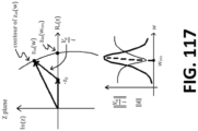
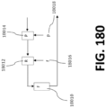
- the ATLXR and its operation may be described using a pole zero diagram of the open loop response of the ATLXR.
- a loop delay needs to be represented which includes module delays of:
- the pole zero plot of the open loop ATLXR response is shown in FIG. 181 .
- the s plane is shown with vertical axis as the jw axis, and the horizontal axis as the real axis. Also shown are the poles of a Pade delay model 18110.
- the set of poles 18110 and zeros 18112 shown as the 'Pade model of the open loop delay' of FIG. 181 is a polynomial approximation to the phase exponential term of exp(-sTD), where TD is the overall accumulated delay of the signal loop that does not include the delay of the primary or adjustable resonators.
- the Pade poles and zeros are equivalent and not physical. They form an all pass filter structure that affects phase only and not amplitude.
- Pade poles and zeros of FIG. 181 an essential observation is that these equivalent poles are far into the left-hand plane relative to a) the tunable poles of R, and b) the higher Q poles of the primary resonator. Also, for the closed loop the pole migration with increased loop gain of the Pade poles is negligible.
- FIG. 182 shows the poles and zeros of the Pade representation for a normalized loop delay of two periods of the ATLXR band center frequency.
- the effect of increasing the loop delay further is that the poles move closer to the jw axis and therefore influence the phase slope more.
- a higher order Pade model will be needed. Instead of this, the Pade poles and zeros could be expressed more as a bandpass response. However, this is not really necessary as the delays will be small.
- the Pade delay model accurately represents the effect of the arbitrary delay that occurs within the signal loop.
- the operation of the ATLXR is then explained based on FIG. 183 .
- the ATLXR loop gain g is increased, the dominant high Q pole of the primary resonator closest to the j ⁇ axis will follow one of the trajectories as shown by the small arrows. The trajectory followed depends on the location of the pole of R (as controlled by f) and the phase setting of P.
- variable secondary resonator R is adjusting the s-plane operating point of the primary, or external resonator XR.
- the ideas developed herein are applicable to a device in which the ATLXR places a controllable variable resonator (R) with a variable gain block into a signal loop that includes an external generally high Q resonator (XR), such that the closed loop frequency response of the ATLXR that incorporates the primary, or external resonator XR may be modestly "manipulated".
- This manipulation of the primary external resonator is actually a manipulation of the closed loop ATLXR circuit that contains the primary resonator, and the tunable resonator.
- Dynamic modifications of the closed loop ATLXR are sufficient to get the desired passband response and compensate for moderate temperature changes, initial manufacturing tolerances, and device ageing effects of the primary, or external resonator XR.
- the closed loop resonance effecting the signal path transfer function from the input to output port is a modified version of the dominant resonance pole of the stand-alone primary resonator.
- the transfer function from the input to output port of the ATLXR results in a narrow bandpass frequency response that is approximately equivalent to the response of a single dominant high Q pole that can be manipulated with the controls ⁇ f,g,p ⁇ acting on the secondary variable resonator R
- the pole of the primary resonator which may not be explicitly controllable, may be implicitly controlled to move the pole a desired location in the s-plane by operation of the coupled signal loop, for such items as, but not limited to:
- a frequency hopping sub-band such as in Bluetooth
- the overall SAW may provide a 20 MHz bandpass
- the ATLXR emphasizes the particular sub-band of 1 MHz bandwidth, and follows the frequency hopping scheme.
- XR(s) is used to represent the transfer function of the external resonator, which may be considered external to the ATLXR chip.
- the XR resonator may be any electrical, electromagnetic or electro-mechanical resonator, such as the following:
- the ATLXR variable resonators R are generally low Q resonators, may be integratable onto a chip, and may be controllable in terms of frequency response for both resonance frequency and bandwidth. Examples of suitable resonators R in the ATLXR shown above are broadly described above.
- R(s) is the transfer function of the secondary resonator of the ATL signal loop and has a control of f.
- the control f would typically act on a form of varactor diode, or perhaps a MEMS device, to vary the capacitance of R.
- P is a discrete switched phase that may have several phase states as selectable by the control of p.
- the gain block G has a variable gain controllable by g. Finally, there is a coupler at the input and output of the ATLXR circuit.
- variable R resonator would ideally be integrated on chip.
- R would typically consist of integrated capacitors and spiral inductors of fixed value in addition to a varactor diode of variable value as controllable by f.
- R may also be implemented based on distributed transmission line components integrated onto the chip die.
- Another alternative for the resonator of R is that it is implemented based on an integrated MEMS device which results in a variable inductor or variable capacitor. Examples of suitable resonators R may include those described in detail in Nielsen.
- the primary resonators may be single port instead of two port devices.
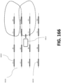
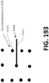
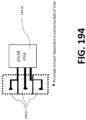
- a multiple pole BAW chip device as illustrated in FIG. 191 .
- the resonators are on a common BAW chip with grounding and one port connections from each resonator to the ATLXR chip.
- Proposed is an external resonator chip consisting of a plurality of BAW resonators each with a one port connection to the matching ATLXR chip that constitutes a multipole filter.
- the internal adjustable resonator block R closes the signal loop as required.
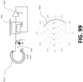
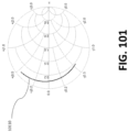
- the primary resonator may be part of an antenna or radiating system. This may include antennas that have some resonance property as a chip antenna or a printed circuit antenna.
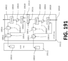
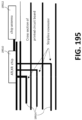
- An ATLXR may be arranged as shown in FIG. 192 which has a plurality of general ATLXR blocks and a switch matrix that connects various antennas and various resonators. This will have general ports that may attach to BAW resonators, printed resonators, chip antennas, no resonator at all, etc. On the other side the switch matrix attaches to ATLXR circuits. Or if no enhancement is required then no ATLXR is attached.
- FIG. 192 shows BAW/SAW resonators 19210, PCB printed resonators 19212, chip antennas 19214, switch matrix 19216, block of ATLXR circuits 19218, and general ATLXR chip 19220.
- the switch and plurality of ATLXR circuits may be integrated into a generic transceiver chip and then general external resonators may be attached to the general pins of the ATLXR which may be antennas, printed circuit board resonators, SAW/BAW resonators, and the like.
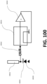
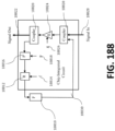
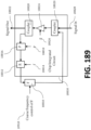
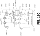
- FIG. 188 shows components F 18810, R 18812 controlled by f 18814, P 18816 controlled by p 18818, couplers 18820, signal out 18822, gain block G 18824 controlled by g 18826, signal in 18828, and chip integrated circuit 18830.
- the signal loop may have a single variable resonator or a plurality of variable resonators. Further, there may be one or more primary resonator, either in series or in parallel, connected in series within the loop with the one or more variable resonators.
- the adjustable resonator may be integrated on chip.
- the adjustable resonator may consist of integrated capacitors and spiral inductors of fixed value in addition to a varactor diode of variable value as controllable by f.
- R may also be implemented based on distributed transmission line components integrated onto the chip die.
- Another alternative for the resonator of R is that it is implemented based on an integrated MEMS device, which results in a variable inductor or variable capacitor.
- Other suitable resonators will also be recognized by those skilled in the art.
- the ATLXR signal loop has an adjustable resonator R, coupled with a primary, or external resonator, which may be of various types. This permits a combined closed loop resonator response with a single dominant pole that may be manipulated with the controls ⁇ f,g,p ⁇ within the secondary tunable resonator.
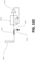
- the primary resonator F may be controllable or tunable between different operating frequencies, as in the example of FIG. 189 , having components F 18810, R 18812 controlled by f 18814, P 18816 controlled by p 18818, couplers 18820, signal out 18822, gain block G 18824 controlled by g 18826, signal in 18828, and chip integrated circuit 18830, and additionally having coarse frequency control ofF 18910.
- the primary resonator may be a ferrite based resonator with an applied magnetic field for slow control.
- it may be a MEMS type resonator that has some coarse frequency control that is relatively slow.
- the ATLXR may be directly extendable itself to a multi-pole filter implementation.
- FIG. 190 shows components F 18810, R 18812 controlled by f 18814, P 18816 controlled by p 18818, couplers 18820, signal out 18822, gain block G 18824 controlled by g 18826, signal in 18828, and chip integrated circuit 18830, and additionally having variable attenuator 19010 controlled by v 19012.
- the additional control of v for the variable attenuator V is provided such that the overall throughput gain of the multi-ATLXR circuit does not result in uncontrollable self-oscillation.
- the cascade configuration of FIG. 190 is extendable to an arbitrary order bandpass filter wherein each ATLXR circuit will implement one SOS (second order section or bi-quad) of the overall transfer function of the bandpass filter.
- Integrated chip complexity is generally considered to be secondary as small signal transistors may be integrated at negligible cost. Inductors and capacitors may be costlier as they occupy a larger die area. Hence a cost-effective integration of the variable R resonators generally only achieves a low Q value of about 10. To achieve a highly selective bandpass filter response, it is necessary that the filter poles have high Q values, e.g. much higher than 10, and therefore significant Q enhancement may be necessary. While arbitrary high Q enhancement is possible with the ATLn, this comes at a cost of reduced linearity. The advantage of the off-chip external resonator is that it may have a fairly high initial Q and hence only a modest further enhancement in Q is necessary.
- the primary resonator will have a Q that is about 10 times or more greater than the Q of the adjustable resonator, and may be as much as 100 times or more greater than the Q of the adjustable resonator.
- referring to the values of 10 or 100 is not intended to be a definite limit, but shall be considered a general range that will inherently unclude factors that are close to, but may be slightly outside, these ranges.
- the primary resonator may be an external resonator.
- the term "external” is commonly used herein to refer to the primary resonator.
- teachings may also be applied to non-external resonators.
- a resonator may be considered external if it is made from a different material, or a different technology, relative to the adjustable resonant circuit.
- the primary resonator may be a first component, made form a first material
- the adjustable resonator may be a second component made from a second material that is different than the first material. Exmaples of this are shown, for example, in FIG. 188 , where the resonator is "off-chip" relative to the adjustable resonator, and in FIG. 191 , which shows a BAW filter on a separate substrate. Other designs will be apparent to those skilled in the art and will not be discussed further.
- a useful printed resonator may include a waveguide-like cavity built on the PC board with a number of via connections to contain the field. This is shown in FIG. 193 , which is a top down view of the resonators showing the feed structure and the via hole connections that stitch the outer periphery of the waveguide cavity. Via connections in the PCB are shown at 19310, and the feed is shown at 19312. Metallization at the top and bottom planes of the printed circuit board are not shown for sake of clarity. A single port resonator is shown but this could be a two port by adding another feed probe.
- a resonator of this type has the advantage of providing higher Q as the losses are essentially dielectric and not conductive.
- Multiple resonators 19412 may be implemented as shown in FIG. 194 , each of which are connected to an ATLXR chip 19410.
- Multi-level boards offer a possibility of stacking printed resonators as illustrated in the diagram in FIG. 195 having ATLXR chip 19510 and chip antenna 19512.
- ATLXR chip 19510 and chip antenna 19512 Generally, in smart phones at least 10 layers are used and hence a number of stripline resonators 19514may get stacked as illustrated in order to occupy less space. If the ATLXR chip uses ball grid connectors, then the resonators may be stacked under the chip for compactness. This makes for a very cost-effective implementation of external resonators XR that would have an initial Q on the order of 100 for microwave frequency applications. At higher frequencies, the printed resonators become more attractive as they are smaller but may require low loss dielectric substrates in order to maintain the Q of an external resonator XR at around 100 or so.
- the first characteristic is a set of resonators which are to be coupled, including:
- the second characteristic is an active signal loop that incorporates the set of resonators.
- This generally includes the coupling architecture that couples the signal in and out of the resonators in order to achieve the desired effect.
- Coupling mechanisms may consist of circulators, directional couplers, multiport devices, etc. There may be one resonator or multiple resonators in the loop. Further, the 'resonator' implies the system of resonators unless we are specific about referring to a single resonator.
- ATLXR Implementation Category 1 Unidirectional Signal Flow
- Category 1 is the first ATLXR implementation category, and has two main characteristics. The first is that all of the signals are unidirectional. The second is that the input signal is isolated from the feedback signal via the directional sum block. This however assumes that the sum block is nonreciprocal.
- a better way to implement ATLXR Category 1 is to use an active differential amplifier 20502 as a non-reciprocal sum block that forces the unidirectional signal flow in the loop, as shown at the top of FIG. 205 , where the circuit on the top has a resonator 20504, a phase shifter 20506 and a gain block 20508, and the circuit on bottom has ATL circuits 1301 and an external resonator 20510.
- the output may be taken anywhere, and the order of the components in the loop is arbitrary. While the resonators are labeled 1301 in the various drawings depicting ATL circuits, it will be understood that these may be higher or lower order ATL circuits, or may be a basic resonator, such as resonator 1401 discussed previously.
- This active feedback summer is perhaps ideal in that the differential amplifier circuit is trivial to implement on chip and does not require any inductors or other components that are difficult to implement at chip level.
- the ATL3 implementation enables loop phase shift control within the low Q secondary resonators, and a phase shifter may be as simple as switching between two phase polarizations.
- ATLXR Implementation Category 2 Bidirectional Signal Exchange with the External Resonator
- Category 2 implementation of the ATLXR uses either a directional coupler or a circulator as the combining element between the primary resonator (XR) and the adjustable resonator circuitry, as shown at FIG. 110 and FIG. 206 respectively, where an implementation using either the ATL1 or ATL3 is shown as the adjustable resonator circuity.
- Other ATL implementations are also possible.
- the circulator or directional coupler backwards so as to deliberately reflect the feedback signal off the external resonator as an input component that now becomes part of the loop.
- the role of the circulator or directional coupler is to separate a bidirectional flow in the external resonator to a segregated flow in the loop.
- a reversed directional coupler 20704 of say 10 dB
- this provides a signal to bounce off of the antenna 20702, shown at the top of FIG. 207 , or to the input of an external resonator such as a BAW or printed circuit antenna as the external one port resonator that is recirculated, as shown at the bottom of FIG. 207 , where the circuit also includes a resonator 20706 and a gain/phase block 20708.
- the external resonator is an antenna
- the ATLF the ATLF in detail below
- ATLXR Implementation Category 3 The ATL as a Negative Resistance Amplifier
- Category 3 implementation of the ATLXR uses a hybrid coupler, as shown at the bottom of FIG. 113 where the ATL is implemented as a negative resistance amplifier. In this implementation category, there is no requirement for a directional coupler.
- the hybrid coupler is part of the in-line bidirectional phase shifter. It is an example of an implementation of a phase shifter and does not really have anything to do with the ATLF feedback loop. That is, a phase shifter may be developed in another way without the hybrid coupler.
- ATLXR Implementation Category 4 Using External Two-Port Resonators
- ATLXR Category 4 consists of the external resonator as a two port resonator. This two port resonator could be a printed antenna, a printed resonator, or a two port BAW/SAW. Category 4 is shown in FIG. 209 , with an antenna 20902, resonator 20904, and a gain/phase block 20906. As such we can envision an application of, for instance, a multiple pole BAW chip device as illustrated in FIG. 191. FIG.
- FIG. 191 shows components F 18810, R 18812 controlled by f 18814, P 18816 controlled by p 18818, couplers 18820, signal out 18822, gain block G 18824 controlled by g 18826, signal in 18828, ATLXR chip 19110, BAW chip 19112, and attenuator 19114 controlled by a 19116.
- the resonators are on a common BAW chip with grounding and one port connections from each resonator to the ATLXR chip.
- Proposed is an external resonator chip consisting of a plurality of BAW resonators each with a one port connection to the matching ATLXR chip that constitutes a multipole filter.
- the internal resonator block R forms the additional feedback port required.
- An ATLXR may be arranged as shown in FIG. 192 which has a plurality of general ATLXR blocks and a switch matrix that connects various antennas and various resonators. This will have general ports that may attach to BAW resonators, printed resonators, chip antennas, no resonator at all, etc. On the other side the switch matrix attaches to ATLXR circuits. Or if no enhancement is required then no ATLXR is attached.
- the switch and plurality of ATLXR circuits may be integrated into a generic transceiver chip and then general external resonators may be attached to the general pins of the ATLXR which may be antennas, printed circuit board resonators, SAW/BAW resonators, and the like.
- Wireless transceivers have been highly integrated and optimized over the past decades to a point where a sophisticated WiFi transceiver, operating at 2.45 GHz or 5 GHz, consists of a small number of components enabled by the high level of integration in the central transceiver chip, and fits onto a circuit board of several square centimeters. This has fueled the IoT and applications such as the wireless smart bandage sensor.
- the availability of inexpensive wireless transceivers is now creating a push for even further cost reductions, performance enhancements, and antenna size reductions.
- ESA Electrically small antennas
- an antenna is easiest to understand if we start in the transmit mode. It is simply an apparatus that arranges current flow of charge that is alternately accelerating and decelerating such that radiated electromagnetic (EM) fields have an amplitude that depends inversely on the range from this radiating apparatus in the far field that is typically 10 wavelengths from the radiating source.
- EM radiated electromagnetic
- the Lorentz reaction integral predicts that the performance of the receive antenna is reciprocal to the performance of the transmit mode antenna: the current distribution within an antenna and the antenna impedance is the same for both transmit and receive functions. Hence we can analyze the antenna in transmit mode and use the impedance properties calculated to determine the behavior of the antenna in the receive mode.
- FIG. 53 shows a remote source 5310, a radiation wave 5312, and wire dipole 5314.
- the Lorentz reaction integral which is the measure of how the antenna structure couples to the incoming external field, is ⁇ s E • J ⁇ H • M d ⁇
- the current distribution within an electrically small wire antenna may be determined from the same Lorentz reaction integral by determining the current distribution that has:
- the input impedance is then easily extracted once the antenna current distribution is known.
- the Lorentz reaction integral provides a way to calculate the general coupling between the two antenna structures.
- the Lorentz reaction integral shows that the coupling is reciprocal: coupling is independent of which antenna is radiating and which antenna is receiving. A significant result from this is that the antenna impedance is the same for both transmitting and receiving.
- This principle of reciprocity allows us to analyze the antenna as a transmission structure, which is usually simpler, and then directly use the outcome of this to reciprocally tell us how the antenna receives a signal. In the transmit mode, accelerating electrons moving along a wire conductor generate EM fields that have a 1/r component, r being the distance from an observation point to the antenna center.
- the input impedance and conductance of a dipole antenna of variable electrical length are presented in FIG. 54 , where electrical length is the total physical dipole antenna length in terms of wavelengths.
- the real component is shown at 5410, while the imaginary component is shown at 5412.
- the antenna behaves as a capacitor and for longer than resonance behaves as an inductor.
- the series LRC dipole impedance model is a reasonable approximation, as the slope of the real component is not overly steep.
- the LRC model of a dipole antenna may only be accurate over a relatively narrow bandwidth for higher Q dipole antennas.
- the half wavelength dipoles, or even quarter wavelength monopoles are physically too large for small wireless sensor applications and a more compact antenna is required.
- FIG. 55 we consider the input impedance of a small antenna with a dimension of nominally 0.1 wavelengths.
- the series LRC model of such a short dipole shows that the radiation resistance is 2 ohms while the series capacitive reactance is 2000 ohms. It thus requires a resonance circuit of very large Q and component precision to efficiently compensate for this large capacitive reactance. It is a non-trivial impedance matching circuit to transform the 2 ohms to 50 ohms.
- FIG. 56 shows the impedance of an electrically small dipole wire antenna with an antenna Q on the order of 10 to 20 over a 20% relative bandwidth.
- This antenna structure generates primarily a magnetic field perpendicular to the loop plane, which is equivalent to a (fictitious) magnetic current dipole also perpendicular to the loop plane.
- An equivalent representation of this antenna is a magnetic current M flowing perpendicular to the plane of the loop. Note that M is fictitious, unlike J which is real.
- the Lorentz coupling integral of the loop antenna becomes ⁇ v H ⁇ M dv showing that the loop antenna is now sensitive to the magnetic component of the far field external source instead of the electric component
- Impedance matching is in principle accomplished by a series capacitor of - jX( ⁇ ) that resonates with the antenna inductance, providing an R( ⁇ ) which is generally on the order of several ohms: a resistance that is too small for compatibility with low power integrated electronics.
- Segment 5710 of the Smith Chart curve (normalized to 50 ohms) shown in FIG. 57 is the series capacitor and 5712 is the shunt capacitance. Note that this only matches the antenna for one frequency. If it is desired to be well matched over a larger range of frequencies then, a more complex impedance matching circuit would be required.
- ground Plane Effects The dipole and loop antennas are balanced in the way that they are symmetrical with regard to the terminal. However, in the construction of small wireless circuits a ground plane is convenient as it forms a potential reference point that is distributed throughout the circuit. Unfortunately, as the frequency increases, a ground plane:
- the printed antenna such as the inverted F antenna (PIFA) is inexpensive and efficient.
- the PIFA antenna is an example of an unbalanced antenna with a ground plane. This is commonly used as a printed antenna for small wireless transceivers.
- FIG. 211 shows the current flow and the resultant field generation, represented by arrows 21102, complicated by the current flow in the ground plane.
- the size of about quarter wavelength may still prove to be prohibitive.
- Aperture antennas The wire dipole and the wire loop are the two fundamental types of radiating structures: all wire antennas are combinations of these two antenna types. While aperture antennas that couple into waveguide structures are different, these are not of significance in this discussion except to say that in order to couple from a field mode to a conducted mode, a wire antenna of some sort is still needed.
- Chip antennas are generally installed such that the ground plane is a significant circuit element, with the ground plane essentially forming the other half of the antenna.
- FIG. 59 shows an antenna 5910, filter network 5912, and transceiver 5914.
- the circuit ground plane essentially forms the other half of the antenna adding more impedance matching complexity.
- the transceiver has to (generally) provide matching typically to 50 ohms, which implies internal buffering with an impact on overall efficiency.
- the matching components not only add cost, but also require board space; additional fabrication steps; and are lossy. Referring to the bottom of FIG. 59 , a transceiver chip with ATLn 5916, a chip antenna 5918, and a ground plate 5920 are shown.
- a varactor diode may be placed as a shunt component from the chip antenna terminal to ground. Similar to the resonator of the ATL1, this allows for a smooth tuning across a broad frequency range.
- the ATLn directional coupler when integrating the ATLn with an electrically small antenna, is realized based on using spiral transformers and inductors. For a desired tuning bandwidth of over 10%, it is difficult to achieve good directivity such that the coupling ratio
- a solution might be to include a low noise amplifier (LNA) between the antenna and ATL1. However, this will require additional components to match the antenna with the LNA, or else a significant portion of the available power will be reflected back to the antenna and re-radiated.
- LNA low noise amplifier
- the adjustment of a circuit referred to as the ATLF may be accomplished by allowing for an automatic conjugate impedance match between the antenna and the receiver, as discussed elsewhere.
- the ATLF may be used to achieve a high degree of energy transfer between the antenna and the transmitter/receiver, and does so at the specific band of interest within the larger frequency envelope of the modulated signal carrier.
- FIG. 54 shows the plot of the input impedance and conductance of a dipole antenna of variable electrical length, where electrical length is the physical length in terms of wavelengths. For lengths shorter than resonance, the antenna behaves as a capacitor and for longer than resonance behaves as an inductor. Of interest is that in neither the series LRC antenna model nor parallel LRC antenna model is the real part constant since the antenna radiation resistance is a function of electrical length.
- Such small ESAs have a high reactive component and a low radiation resistance.
- FIG. 55 we consider the input impedance of a much shorter antenna of nominally 0.1 wavelengths.
- the series RC model of such a short dipole shows that the radiation resistance is scarcely 2 ohms, while the series capacitive reactance is 2,000 ohms. It requires a resonance circuit of enormous Q and component precision to efficiently compensate for this large capacitive reactance.
- the matching circuit to transform the 2 ohms to 50 ohms is not trivial and using actual lumped matching components represents a significant loss.
- FIG. 56 shows the impedance of a dipole that is nominally 0.35 wavelengths long.
- the radiation resistance has increased to 30 ohms, while the series capacitive reactance is a more manageable 375 ohms.
- This fixed impedance antenna is subsequently attached to a matching fixed impedance transceiver subsystem.
- Signal loss in the coupled antenna/transceiver system the antenna impedance matching of the antenna, over the operating range of the transceiver, is a fixed and relatively constant average impedance over the operating band of the transceiver. The result is a loss of some 2 - 3 dB in signal strength for both transmit and receiver. This loss in signal strength reduces the range of the transceiver.
- a conjugate matching antenna circuit may be used that allows for a maximum or at least increased amount of energy transfer between an ESA antenna to the transceiver over the entire bandwidth of the transmission.
- This circuit is called the Anlotek ATL Filtenna, or simply the ATLF.
- the ATLF is applicable to both transmit and receive functions.
- the ATLF conjugate matching antenna circuit is functional in conditions where the antenna impedance is not static.
- control of a circuit for complex conjugate matching of an antenna in a situation or application where the local environment of the subject antenna causes the reflection coefficient of the subject antenna is not static.
- the change of the reflection coefficient may be caused by 1) local environmental factors, or 2) the coupling of the subject antenna with nearby objects, or 3) application specific changes to the antenna impedance.
- Antenna optimization techniques for communication systems and other applications in such a dynamic environment may lose track of the true reflection coefficient of the subject antenna and thus fail to optimize the antenna or even cause the antenna to be effectively decoupled from the transceiver system.
- VSWR Voltage Standing Wave Ratio
- This method looks at the VSWR present in the signal transmission line to the antenna as a measure of impedance mismatch between the transmitter and antenna and adjusts variable inductor and capacitor circuit elements to minimize the VSWR.
- Variable line length elements are another way of minimizing the VSWR. Measuring the VSWR requires special equipment at the antenna tower.
- the VSWR is adjusted to minimize the impedance mismatch at the antenna across the full bandwidth of the transmission. This is in marked contrast to the approach discussed below that optimizes the matching between the antenna and the receiver / transmitter.
- reconfigurable antenna may be used to refer some sort of control applied to the antenna to change its frequency response or radiation pattern. This may be achieved by a varactor diode control or PIN switches to couple in different parts of the antenna.
- a varactor based tunable antenna which thereby falls into the definition of a reconfigurable filtenna, has a response as shown in FIG. 61 .
- Many other examples of the reconfigurable filtenna exist in the literature, one category using active secondary radiators for achieving the reconfigurable filtenna properties.
- the ATLF coupled resonant structure antenna subsystem reduces or removes the need for impedance matching when connected to a circuit as the antenna feed. This form of antenna impedance matching by the ATLF is valid for both transmit and receive mode. Additionally, the ATLF resonator-linked antenna subsystem also allows for an improved transfer of received antenna energy to the attached transceiver.
- the ATLF accomplishes impedance matching by synthesizing the unknown reflection coefficient of the antenna, by which the ATLF creates an equivalent conjugate impedance match with the receiver, which is the condition for maximum energy transfer from the antenna to the receiver.
- the actual reflection coefficient of the antenna is dynamic and unique to the antenna structure at the precise operating frequency but is not known a priori by the ATLF.
- This synthesizing of the unknown reflection coefficient of the antenna is achieved by analyzing the SNR feedback from the receiver demodulation, available from the receiver system, and dithering both magnitude and phase within the ATLF to provide the conjugate impedance match sought. Once this is achieved, the ATLF may further increase the magnitude of the effective reflection coefficient thereby effectively narrowing the signal bandwidth and increasing the Q of the received signal. Bandwidth narrowing is limited by the self-calibration and stability control of the ATLF, discussed below, that assures stability by preventing the feedback loop from driving the ATLF into instability by crossing the j ⁇ axis and crossing into the RHP.
- lookup table parameters may be used for optimization, rather than the demodulated SNR feedback from the receiver.
- transmitter matching is based on feedback from the receiver, as the SNR estimation sets appropriate values stored in a LUT that may be used for the transmit mode, based on the principle of reciprocity.
- the ATLF resonator linked antenna subsystem shown as two coupled resonators in FIG. 62 in the receive mode, thus dispenses with the typical antenna matching components and allows connecting the transceiver device directly to the ATLF resonator linked antenna subsystem.
- FIG. 62 shows an impedance unmatched antenna 6210, a recirculating loop at antenna and ATL port 6212, an ATL resonator 6214, an ATL gain block 6216, and received signal output 6218. This is possible because any electrically small low loss antenna is a resonator circuit element in itself that would be absorbed into the ATLn as a resonator sub-circuit such that they resonate together.
- the ATLF may be used as:
- the increment in the chip die size to accommodate the ATLF is an insignificant cost driver.
- the inductor is more of a size issue and Q's of more than 15 are not likely cost effective.
- the ATLn resonator Q of about 10 is a reasonable starting point.
- a successful ATLn enhancement factor ratio of closed loop Q to open loop Q
- the ATLF is described below in terms of an ATL-based circuit. It will be apparent, however, that circuits that provide similar benefits, to a greater or lesser extent, may be provided using other components that perform similar functions as those performed by the ATL-based circuit.
- the circuit connected to the antenna includes a signal conditioning block that includes an adjustable phase shift element and an adjustable scaling block connected in a signal loop with the antenna, where the adjustable phase shift element and the adjustable scaling block are controlled to condition the signal to modify the signal received by the antenna toward a desired signal.
- the signal conditioning block also includes an adjustable resonator. It will also be understood that the signal conditioning block may be divided into separate components and distributed throughout the signal loop to provide the desired signal conditioning.
- D r is fixed based on what can be easily integrated into a chip.
- D r 0.05 is reasonable for an integrated LC chip resonator resulting in a resonator Q of 10, which is easily designed.
- a key point here is that such a low Q means that the resonator components may be physically small when integrated.
- L and C are the integrated inductor and capacitor components of the resonator.
- L and C should have a small value, as the physical area of each component grows roughly proportional to the component value.
- ⁇ r the resonance frequency
- the energy storage in L is 0.5 Li 2
- the energy storage in C is 0.5 Cv 2
- i and v are the current and voltage of the resonator signal.
- i and v are the current and voltage of the resonator signal.
- the directional coupler 6410 adds the resonator output back into the loop and minimizes the connection to the input port 6420.
- the directional coupler 6410 is of value in this context as the recirculating signal is of much larger amplitude than the incoming signal by a ratio (at resonance) of 1/(1 - G), where G denotes the overall open loop gain at resonance, as controlled by the control voltage g. This signal ratio results in a large return gain on the input port 6420 of the ATL.
- the splitter in FIG. 64 may be trivially implemented with a simple lossy resistive circuit.
- phase shifter for the ATL1 is discussed above. Now consider the combining of the phase shifter into the feedback loop of the ATLF, shown in FIG. 68 , consisting of resonator 6810, a gain element 6812, a phase shifter 6814, a directional coupler 6816, input 6818, and output 6820. As indicated herein, there are various implementations of circuits available to provide the directional coupler function.
- the numerator of this transfer function may vary depending on where the output and input are given. For now, we assume the input is current impressed into the antenna and the output is taken from the output of the gain block. Now we can consider the combined poles and zeros and plot out the closed loop poles as a function of G as shown in FIG. 69 .
- the resonator poles move towards the jw axis as G is increased, eventually crossing the line with the maximum ingress into the right hand plane being the open loop zeros of the phase shifter all-pass network.
- the open loop poles of the all-pass filter go conveniently deeper into the left hand plane and become the secondary closed loop poles.
- FIG. 69 we show the case for the aligned phase shifter and resonator. If the phase shifter is misaligned, then a distorted root trajectory results as shown in FIG. 70 . Note that the resonator ⁇ r would have to be adjusted to compensate for the phase error of the phase shifter to get the same ATL1 center frequency.
- the rule for optimizing the three control voltages ⁇ f,p,g ⁇ still holds and may be generalized as: Given the constraint of a given output ⁇ signal level, Q enhancement, bandwidth ⁇ then ⁇ f,p,g ⁇ is set such that g is minimized, where
- the Nyquist plot can be used to show the effect of adding additional delay to the loop, such that there are multiple 360 degree increments associated with the round trip delay.
- excess delay increases in the ATL1 loop, there is a narrowing of the passband as the off-resonance points are significantly moved due to the phase shift of the delay.
- FIG. 73 shows a Nyquist plot of XR(s) as the delay increases from no delay (line 7310) to finite delay (line 7312) and then infinite delay (line 7314).
- the circuit of FIG. 75 may be approximated as the circuit shown in FIG. 76 , having source 7610, resistor 7612, and terminating in Z load 7614.
- the impedance looking into the matching network and receiver from the antenna is exactly 20 ohms. Also, as only lossless inductors and capacitors are used in the match, the full available power from the antenna is dissipated in the receiver resistance R r .
- the L match is simple and works well for narrow bandwidths.
- a problem with a chip integration of the L-match is that the range of L and C required to accommodate a range of antennas may be significant.
- a tunable inductor could be implemented with a MEMS device.
- MEMS do not integrate well with standard RFICs or MMICs due to mechanical structures required and high control voltage so when circuit cost is an issue, MEMS solutions are usually not viable.
- the ATLF implementation of a negative resistance device works only at the resonant frequency of the antenna itself. This resonant frequency occurs when the reactance of the antenna is zero. In a practical implementation, a negative resistance device will have some reactance associated with it that will push the resonance. We will first consider the ATLF circuit with a fixed frequency negative resistance device, and then extend that treatment to a variable negative resistance implementation, providing tunability.
- Attaching a negative resistance device to the antenna may be approximated by the circuit shown at the top of FIG. 112 .
- the circuit in FIG. 112 shows antenna model 11210 with resistor 11212, capacitor 11214, and inductor 11216, along with coupling cap 11218, and negative resistance provided at resistor 11220 and inductor 11222.
- the root locus and Nyquist plot of this circuit are shown at the bottom of FIG. 112 .
- Application of a larger magnitude of negative resistance pushes the magnitude of the ATLF reflection coefficient over one and results in Q enhancement. Note how the poles circle around and cross the jw axis at a much different frequency than the resonance of the antenna. Also, there are two resonances with the second occurring at a much lower frequency. This is evident in the Nyquist plot also.
- the antenna may have a soft resonance, but as gain is increased the Q enhancement may change the band center completely and seemingly unpredictably. This is where the ATLF provides much more predictable control of the Q enhanced passband.
- phase shifter consisting of a directional coupler and varactor diodes.
- Putting this four port directional coupler into the scheme of FIG. 113 results in a phase shift equal to the phase shift of the reflection of ports 2 and 3, facilitated by a change in the varactor diode voltage.
- the top portion of FIG. 113 shows antenna 11310, directional coupler 11312, gain block 11314, output 11316, phase shifter 11318, and termination 11320.
- the middle portion shows antenna 11322, bidirectional hybrid coupler and phase shifter 11324, and negative impedance 11326.
- the bottom portion shows antenna 11328 connected to resistor 11330, capacitor 11332, and inductor 11334, with hybrid coupler 11336 and negative impedance amplifier 11338 having capacitor 11340, inductor 11342, and resistor 11344.
- Hybrid coupler 11336 is also connected to two varactor diodes 11338.
- the signal loop is as follows:
- the directional coupler may provide a 3 dB or a higher coupling ratio. Also, it may be implemented as a 90 degree or a 180 degree coupler.
- the 90 degree coupler is lossless with no signal sent to port 3 such that there is no dissipation in the termination resistor. Hence at resonance the full signal is sent through port 4 into the feedback loop. Furthermore, with ideal components at resonance with the phase shifter set correctly, there is no loss in the circuit, and all the power generated is available to the input port of the 3 dB output power splitter. The result is that when the phasing is done correctly, such that there is ideally no loss in the loop, then the noise figure (NF) of the ATL1 is minimized. Hence this arrangement provides the best NF and the highest frequency selectivity.
- negative resistance amplifier examples include, but are not limited to, a tunnel diode, a Gunn diode, or an Impatt diode.
- a properly biased FET of any type to provide a negative resistance.
- Such implementations are considered known to those skilled in the art. It is important to note that the phase shifter is traversed in both directions.
- phase shifter imposes some loss. Further, the coupler is not integratable at chip level.
- the coupler is not integratable at chip level.
- the scheme 11510 at the top of FIG. 115 uses a variable RC time constant.
- the bottom scheme 11512 uses several stages of inductors and capacitors. Both schemes 11510 and 11512 show resistors 11514, inductors 11516, and capacitors 11518.
- the needed phase delay correction may be minimized by integration.
- the phase shift through the components may be reasonably accurately known.
- fixed phase compensation may be included, and then the phase shifter need only adjust for the phase error or the phase shift not correctable by fixed networks, such as a variable phase shift of a delay over a broad frequency range.
- a simple variable phase shifter may be used that combines the ATL negative resistance implementation and the phase shifter discussed above.
- the objective of the ATLF is to synthesize the physical capacitor of the inductance matching example. This is achieved through matching of reflection coefficients: if the reflection coefficient of the ATLF looks like that of a capacitor, then the circuit will react as if a physical capacitor was actually creating the reflection coefficient. In this case, the antenna reactive inductance is cancelled out.
- FIG. 81 shows a source 8110, resistor 8112, inductor 8114, and RF voltage source 8116.
- the current that flows out of the antenna is i(t) which is reduced due to the inductive impedance.
- FIG. 82 shows source 8210, resistors 8212, inductor 8214, and capacitor 8416. Then the voltage across the capacitor is given as 1 2 R ⁇ Cj ⁇
- the region over which the antenna coupling is reasonable diminishes and higher gains are required. This is expected since the active feedback has to match a larger magnitude reflection coefficient of the antenna. As the reflection coefficients become larger, the resonance becomes stronger and the region shrinks.
- Indirect measures of the matching condition in the receive mode may be facilitated by measuring the SNR of the demodulated output with the simple objective of adjusting the matching components such that the SNR is maximized.
- the only sources of noise are the thermal noise of the antenna based on the effective temperature of the environment it is exposed to and the intrinsic noise of the receiver RF amplifier, then maximizing the SNR of the demodulated received signal output is equivalent to minimizing the NF or the FOM as described earlier.
- the NF has the penalty term of 1 / 1 ⁇ ⁇ r 2 which is thereby minimized, which in turn implies that
- ISI noise inter-symbol interference discussed elsewhere
- ISI noise increases as the bandwidth of antenna match becomes too narrow. This is an element of consideration when the bandwidth of the ATLF received signal is too narrow to begin with, as discussed below.
- the first is that the antenna is matched to transfer the maximum signal power to the receiver.
- the second is that the bandwidth is limited by the matching process, due to the resonance of the matching network as discussed below. Hence noise and interference from outside of the resonance peak is being suppressed relative to the desired antenna signal.
- FIG. 89 is then a block diagram of the processing that we are attempting to do, showing the antenna 8910 picking up the signal and being matched to the receiver, whereupon the signal is demodulated extracting the data symbol values used to optimize the information content contained in both the SNR and ISI metrics.
- FIG. 89 shows antenna 8910, impedance match 8912, receiver RF/IF 8914, data demodulation processing 8916, SNR estimate 8918, and SNR optimization algorithm 8920.
- An outcome of this process is also the estimate of the SNR of the samples of the demodulated data symbols. These are used in the SNR optimization that contains an optimization algorithm for setting the parameters for the antenna matching.
- the ATLF may be pre-calibrated with a factory measurement and calibration, with values stored in a LUT.
- the real benefit of the ATLF is to adapt to changes in the antenna characteristics.
- Q enhancement within the ATL it is necessary to precisely determine and implement the feedback. And ultimately, it is the noise in the demodulated signal that matters, not directly the amplitude or bandwidth of the demodulated signal.
- the ATLF should respond to features of the filtering that is done in the demodulation process such as from an equalizer used to minimize ISI and in-band interference. It is necessary that the ATLF adapt dynamically to work in concert with these other systems and not compromise their function. Hence attention to overall processing feedback loops is important.
- the BB output (which could also be near IF) is digitized and goes into a baseband equalizer that shapes the baseband filter to minimize ISI (inter-symbol interference) noise as well as in-band noise.
- the equalizer operates with a relatively fast feedback loop as shown because it has to keep up with channel variations due to multipath effects.
- a variant of the equalizer is the rake receiver and OFDM receiver as used in spread spectrum receivers, in which the channel state is continuously tracked and estimated. Regardless of the details, the purpose is to mitigate effects of channel frequency selectivity as effected by changing multipath.
- the data is extracted from the demodulated baseband signal. Additionally, we get some measures of the SNR from the demodulation process that then drives the ATLF optimization.
- the ATLF is not affected by multipath and does not have to accommodate changes to the wireless channel. However, it needs to accommodate changes to the antenna impedance that occur if there are electromagnetic scattering or absorption objects placed in the near field of the antenna that affect its impedance. Changes to the antenna near field are expected to be much slower and less frequent than changes to the multipath communications channel. Consequently, it is desirable to have the ATLF as an outer slower loop.
- antenna impedance changes are of significance
- the smart bandage where the patient may change position effecting the antenna near field and hence its impedance which the ATLF has to accommodate.
- this change occurs slowly and relatively infrequently in comparison to changes in the room multipath channel.
- the receiver the antenna is connected to a receiver of resistance R R .
- the R r load represents the receiver impedance
- the receiver has a noise figure (NF) of NF r .
- the figure of merit (FOM) of the antenna-receiver may be defined to be this NF. This makes sense as the gain of the antenna-receiver is arbitrary and the FOM should only focus on the receiver's ability to utilize the available power sourced by the antenna.
- the desired signal output of the antenna is generally buried in thermal background noise and interference. Additionally, due to multipath, the exact received signal strength is high variable. Therefore, it is not practical to estimate the condition of the antenna matching from observations of the RF signal.
- the desired signal has to be down converted, filtered and processed before structural features of the signal may be reliably measured from which we may assess the state of the antenna matching.
- the reflection coefficient of the antenna may be measured directly based on the VSWR (voltage standing wave ratio) measurement which is typically straightforward to implement.
- VSWR voltage standing wave ratio
- the ATLF consists of an antenna resonator coupled to a resonant ATL self-configured as a negative resistance, shown at the top of FIG. 94 .
- the antenna resonator is represented by the series LRC model, where R represents the radiation resistance.
- ⁇ G G(g) denoting the direct dependence on G as set by the control g.
- ⁇ G G(g) denoting the direct dependence on G as set by the control g.
- ⁇ G G(g) denoting the direct dependence on G as set by the control g.
- FIG. 94 shows antenna (series LRC) 9410, negative resistance 9412, resistor 9414, inductor 9416, and capacitor 9418.
- FIG. 95 shows small loop antenna 9510, capacitor 9512, directional coupler 9514, and gain block 9516. This enables the coupling of the antenna resonator to the ATLn resonator that is central to proper performance of the ATLF. Were not the coupler reversed, the negative resistance reflection from the ATL would feed back into the ATL itself, and not toward the antenna.
- the small loop antenna as an initial configuration as shown in FIG. 95 .
- the gain is arranged as a scaling block and a reversed directional coupler.
- the operation is that the signal enters as a voltage source in the loop antenna. This is amplified by the gain section which behaves as a one port reflection that is reflected back by the mismatched antenna.
- the reversed directional coupler serves to block any reflection from the gain stage controlled by g.
- This reflection coefficient is plotted in FIG. 96 as line 9610 for the normalized frequency range 0.75 ⁇ w ⁇ 1.25. As expected, the C V capacitance cancels the antenna reactance and the reflection coefficient at resonance is a negative real value.
- ⁇ A is a constant amplitude function with a similar pole zero pattern as the all pass filter.
- the root locus for this case as shown in FIG. 97 .
- the output is taken from the scaling block output.
- This root locus shows that the typical ATLn behavior of pole movement exists and may be controlled with closed loop poles crossing the jw axis provided that R ⁇ 1. That is, the radiation impedance is less than the characteristic impedance. If R > 1, then there is a limit to the possible Q enhancement of this circuit as shown in the right side root locus plot of FIG. 97 . Note that when R > 1, the open loop poles are actually on the negative real axis and there is no resonance. Providing feedback, however, does generate Q enhancement from zero to some finite value that is limited by R
- ⁇ A is the negative of the previous case which results in the Smith chart plot on bottom of FIG. 99 with line 9918.
- FIG. 100 shows capacitor 10010, antenna 10012, inductor 10014, directional coupler 10016, and gain block 10018.
- FIG. 98 shows the transfer functions of the ATLF for various values of the normalized varactor diode capacitance. This is calculated by first determining the reflection coefficient of the antenna with matching L and Cv. Then the ideal ATL1 is assigned a reflection coefficient of the smallest real part of the antenna reflection over the frequency range of interest and adding 0.01. This gives a Q in the range of about 100.
- the reflection coefficient is plotted as shown in FIG. 101 at 10110 showing similar behavior as before but the magnitude of ⁇ A is slightly larger and not as symmetric about the real axis.
- FIG. 102 shows antenna 10214, capacitor 10216, directional coupler 10216, and gain block 10218.
- FIG. 103 shows antenna reflection 10310, directional coupler 10312, phase shifter 10314, and gain stage 10316.
- the numerator of this transfer function can vary depending on where the output and input are placed. For now we assume the input is current impressed into the antenna and the output is taken from the output of the gain block. Now we can consider the combined poles and zeros and plot out the closed loop poles as a function of G as shown in FIG. 104 .
- FIG. 106 shows capacitor 10610 and resistors 10612. This restoring circuit may be placed anywhere in the loop of FIG. 103 and provides stable enhancement. With this circuit added, the root locus changes to that of FIG. 107 showing stable enhancement of the dominant pole.
- FIG. 110 shows antenna refection 11010, reversed directional coupler 11012, gain stage 11014, and resonator 11016.
- FIG. 111 The root locus for the ATLF based on the ATL2 is shown in FIG. 111 .
- the poles left of the resonator are the antenna poles and finally to the far left are the poles of the all pass circuit simulating the loop delay.
- a key element of the ALTF is that the directional coupler is reversed from the normal ATLn configuration so that the antenna is coupled into the resonant structure of the ATLn with a controllable bandwidth.
- the normal directional coupler is reversed, this makes the ATLn behave as a negative resistance, providing return gain at the input power.
- the ATLF is implemented in this way, then the requirement for a directional coupler goes away. This may be highly desirable as it is difficult to realize a suitable directional coupler on a chip with L's and C's that are physically small.
- This may be construed as a coupling of resonators, the antenna and the phase shifter.
- the objective here is not a detailed design but rather a discussion of circuit topology such that it may be related back to the ATLF with the ATL1.
- the ⁇ g,p,f ⁇ controls for the ATLF based on look-up table (LUT) entries for a given input of ⁇ desired Q, desired center passband frequency ⁇ .
- the LUT may be populated based on a standardized measurement in an anechoic chamber.
- this initial factory calibration is only of use if the antenna is constant. If the antenna is changed for another or if the impedance of the antenna changes due to near-field interaction then the LUT entries will be in error.
- the ATLF must have to have a run-time calibration method.
- the LUT for the operating point of the data signal (carrier frequency and bandwidth) can be optimized, which optimizes the SNR.
- the inputs to the LUT are the parameters of the data signal, and not the desired center frequency and bandwidth that we use herein for Self Calibration of the ATLn.
- the bandwidth is set appropriately, considering that too wide a bandwidth will result in too much adjacent channel noise to enter the receiver; and too narrow a bandwidth will result in ISI (inter symbol interference).
- the ATLF is still stationary with a static antenna and no changes in the near field but the data signal is frequency hopping.
- the ⁇ f,g,p ⁇ are dithered slightly to a new value and we note if the resulting SNR after the burst has been demodulated has increased or decreased.
- Another complication is that of the change of near field environment of the antenna.
- An example is the smart bandage where the patient may change positions or roll over periodically that influences the near field of the antenna.
- the impedance of the antenna changes and a modified entry for the LUT is required.
- This type of problem has a solution and is covered with extensive publications in the public domain.
- a classic application is the cable modem equalizer.
- the dithering algorithm is the simplest run-time calibration and is generally robust. However, there are pathological cases where the dithering algorithm fails.
- the emerging machine learning algorithms may be applicable. The algorithms will vary significantly with specific applications.
- the signal bandwidth of the ATLF may be visualized by looking at the reflection coefficient into the antenna.
- ⁇ A s 2 + 1 LC s 2 + 2 R L s + 1 LC based on the characteristic impedance being R
- the pole-zero pattern has two zeros on the jw axis and poles in the LHP. The smaller the ratio of R / L the closer the poles will be to the jw axis.
- the signal quality factor of the ATLF which may also be referred to as the figure of merit (FOM), addresses how well the overall antenna responds to an incoming electromagnetic (EM) signal in receive mode.
- This FOM may be flexible in that a variety of antennas may be accommodated by the ATLF, and therefore what is considered acceptable or preferred may change depending on a particular design scenario.
- the FOM therefore has to separate the performance of the antenna element itself and the performance of the ATLF or in other words, the ability of the ATLF to accommodate the specific antenna.
- the antenna intercepts the signal contained in the incoming EM field and converts it into conducted electrical power.
- the efficacy of the antenna to perform this task is quantified by the radiation resistance that is denoted herein as R A .
- the available power from the antenna of course depends on the signal amplitude as either a voltage or current. The complexities of determining the signal amplitude may be ignored in this FOM calculation, as this is simply a property of the antenna and not the ATLF.
- the actual power delivered to the receiver depends on the input impedance of the ATLF and the signal gain associated with the ATLF. However, this ATLF gain should not be part of the FOM. Instead what is important is the ATLF's utilization of the available power and how much noise is contributed by the ATLF.
- R F denote the input resonance impedance of the ATLF.
- FIG. 118 shows resistors 11810 and sources 11812.
- the receiver load resistance R r represents the receiver impedance and that the receiver has a noise figure (NF) of NF r .
- This relationship shows the inflation of the NF due to the mismatch between the antenna and the receiver.
- the figure of merit (FOM) of the antenna-receiver may be defined as this NF. This makes sense as the gain of the antenna-receiver is arbitrary and the FOM should only focus on the receiver's ability to utilize the available power sourced by the antenna.
- the ATLF as a negative resistance generates additional independent thermal noise which may be represented by an equivalent noise source at the input to the ATLF negative resistance block that is characterized by the noise figure (NF) of the ATLF denoted as NF ATLF .
- the NF of the overall ATLF is defined as NF ATLF ⁇ SNR in SNR out where SNR in is the SNR associated with the available power output of the antenna, and SNR out is the SNR at the output of the ATLF assuming that we are evaluating this at the resonance frequency.
- the overall NF of the ATLF is a product of the NF of the negative resistance used in the ATLF ( F F ) and the penalty term of (1-
- NF as a FOM is reasonable as it captures how well the ATLF absorbs the antenna signal and transfers it to the gain stage. This may be compared to conventional arrangements in which the matching circuitry represents component losses and mismatch over the desired frequency range. NF also shows the equivalent noise inflation due to the mismatch of the ATLF, specifically between the antenna radiation resistance and the active electronic device used as the negative resistance. Determining this impedance is a subtle point, as it would seem that
- FIG. 119 shows 4 port directional coupler 11910, gain 11912, resistor 11914, grounding 1196, and phase shifter 11918.
- the output of this coupler is amplified and phase shifted and sent back into the coupler.
- a high ratio coupler such that the pair of ports ⁇ 1,2 ⁇ and the pair ⁇ 3,4 ⁇ are strongly coupled.
- the gain G is sufficiently high such that path from port 1 to the gain G and back through port 3 to port 1 has gain.
- the phase shifter is set correctly to offset the 90 degree shift of the hybrid coupler.
- 2 ) -1 is important but represents a modest loss relative to other loss mechanisms and sources of noise.
- 2 ) -0.9 dB representing a modest increment of about 1 dB in terms of the NF.
- the NF due to mismatch resulting from reactive components may be much larger.
- the main implementation issue of the ATLF is therefore that of resonator coupling.
- various circuit configurations that may be developed, some of which have been arranged into categories, and shown in the block diagrams of FIG. 120 :
- A shows the direct connection from the antenna 12010 to the ATLn 12012, with the ATLn providing frequency tunability and Q adjustment, but without providing coupling to the antenna 12010.
- B shows an LNA 12014 that serves as an active isolator that decouples the antenna subcircuit from the ATLn filter. If the antenna 12010 is not matched to the characteristic impedance over the band of interest, then it will not couple effectively into the ATL1 12012. Hence B includes a matching network 12016 and an LNA 12014.
- C shows the small antenna 12010, which may be modeled as an LRC circuit, where the varactor 12018 modifies the effective antenna capacitance. This changes the antenna resonance, partially matching the antenna over the operating band to the ATL1 resonator 12020.
- D is the same as C, but with a cascade of an ATL1 12020 and an ATLn 12012.
- the first ATL1 interacts with the antenna 12010 and is a lower Q circuit with a varactor 12018.
- the reason for this circuit is to do partial enhancement of the Q creating a dominant pole pair that is further enhanced by the second ATLn. This approach makes it simpler to accommodate a wider variety of antennas.
- E shows the controllable negative resistance solution provided by a configured ATLn, discussed later, to the ATLF implementation.
- E shows antenna 12010, resonator 12022, phase shifter 12024, and negative impedance 12026.
- F shows an ATLF implementation based on an off chip directional coupler.
- F shows antenna 12010, coupler 12028, and scaling, resonator, and phase block 12030.
- G is similar to F but shows that the phase shifter may be removed and replaced by three resonators 12022 that if slightly detuned will provide a suitable range of phase correction, as discussed above.
- G shows antenna 12010, coupler 12028, and scaling block 12032.
- H shows the ATLF comprised of a specialized antenna 12010 that consists of a radiating element 12034 and an integrated directional coupler 12036, providing a two port antenna that may connect to the versions of F and G.
- a specialized antenna 12010 that consists of a radiating element 12034 and an integrated directional coupler 12036, providing a two port antenna that may connect to the versions of F and G.
- control voltages that adapt the performance of the ATLn for the target application may be set, based on the following principles:In this exampleThus, for the ATL1, there may be 3 such LUTs, while for the ATL3, there may be 9 LUTs.
- FIG. 32 presents a circuit that has processing built in for the purpose of calibrating and stabilizing the response of an ATL1 block 7502.
- the microprocessor 7504 generally a system asset, adjusts the control for the frequency and Q of the ATL1 7502 through a DAC implemented as a pulse width modulation (PWM) circuit 7506, and based on readings from a temperature sensor 7508.
- the microprocessor drives the ATL1 7502 to the start to self-oscillation.
- the frequency of this self-oscillation is down converted in block 7510 by a frequency synthesizer signal generated by a crystal reference 7505 and a frequency synthesizer 7507 that is set also by the microprocessor 7504.
- a frequency counter 7509 or other measurement means determines the frequency of the down-converted signal. In this way the resonant frequency of the ATL1 core module may be determined.
- a power detector 7512 and ADC block 7514 that can estimate the rate of increase of the self-oscillation signal at the output of the ATL1 7502.
- the microprocessor 7504 estimates this exponential rise of power and from this determines where the closed loop pole of the ATL1 7502 is. Presently it will be just to the right of the jw axis. If the Q-enhancement is decreased slightly then the self-oscillation will continue at the same frequency to a high accuracy but will begin to decay exponentially.
- the first result from complex variable theory is that the open loop transfer function is in itself stable and has no poles inside the right hand plane. This is true as long as the components are unconditionally stable.
- the resonators and the gain block are assumed to be stable which is certainly true for the resonators, as these are passive sub-circuits with no active gain.
- the gain block may be assumed to be unconditionally stable and hence also qualifies. A situation could arise though if the gain block is based on a transistor configuration that is not unconditionally stable and as the impedance of the other loop components change slightly, could see a pole creep up in the right hand plane that changes the Nyquist stability criteria. This is a design issue that may be avoided or minimized.
- the negative resistance implementation of the ATLF is a bit more challenging in that the gain block is certainly not unconditionally stable. Situations may easily arise in which the reflection off of the resonator or phase shifter and the negative resistance pushes a pole into the right hand plane that is outside of the normal operating band. This could be a frequency well below or above the resonator bandwidth wherein the reflection coefficient approaches unity. This needs to be avoided by careful design insuring that 1) there are no open loop poles in the right hand plane, and 2) potential poles are designed out.
- FIG. 92 shows stable region 9210, unstable region 9212, locus of points with same exponential decay 9214, locus of points with same exponential growth 9216, and outer Nyquist contour 9218.
- the Nyquist locus may have small loops that appear, due to antenna reflections in the antenna near field. These loops are always into the interior of the unstable region as illustrated in FIG. 128 .
- the reason for this is that the phasor of the Nyquist locus (for a realizable stable open loop response) is always in the clockwise direction as frequency is increased.
- the reflection off the scattering points is a much faster rotating phasor that also rotates in the clockwise direction. Sketching this out it is seen that only inwardly oriented loops are possible. This implies that the near field scattering will result in gaps in tunable frequencies. However, as the loops cannot grow on the outside, it helps the stability as the loop will not suddenly make the ATLF unstable. This is illustrated in FIG. 129 .
- the LUT may be populated with the boundary value of the Nyquist locus for the given desired frequency as well as the g giving the desired Q.
- variable multipath and/or variable antenna impedance this is more difficult as the SNR fluctuates randomly. If the multipath and antenna impedance is slowly changing, then we may assume it to be quasi-static, in which case we can complete an iteration of the SNR steepest ascent routine before the characteristics change. In this way we are always tracking the value of g(t) and f(t) necessary for the optimum point. If the fluctuations are slow relative to the time necessary to measure the SNR, then several iterations of steepest descent are possible and we can converge or tightly track.
- each of the set of frequencies is preferably calibrated by the ATLF. Doing so may give us a vector of settings for f and g as a function of the hopping frequency.
- One calibration procedure may calibrate for each of the hopping frequencies as though they were a single frequency. However, another, more efficient procedure may also be used.
- grouping hopping frequencies over the coherence bandwidth of the multipath channel is preferably done in terms of sharing SNR data samples and the steepest descent algorithm preferably converges within the coherence time of the channel. This may seem rather restrictive, however, it is the optimization algorithm only has to keep up with changes in the antenna impedance and some slow changes in the ATLF based on temperature, supply voltage and aging. Hence, the changes to the eventual LUT may be made quite slowly. That said, there will be instances for which the ATLF cannot calibrate and tune properly such as in cases where the sensor antenna is continuously subjected to fast changing and significant near field scattering.
- the calibration will only be developed for that single frequency. It will use the self-oscillation mode to determine the Nyquist boundary point. It may do this several times recording temperature at the same time to start the estimation of temperature related parameters. It then goes to sleep and wakes up when it is time to begin the acquisition phase.
- the calibration is done in the same way but for each of the hopping frequencies as described earlier. Assume that the commissioning provides it with a procedure such that it handles the calibration in an efficient manner such as using a spline fit as opposed to doing each frequency independently.
- the sensor wakes up and begins an acquisition mode.
- the time information may not be exact so that it waits for the packet to arrive at a specific frequency based on the LUT.
- it may do a self-calibration step to fine tune the position of the antenna center frequency and bandwidth.
- the ATLF may not have accurate time information, it will open the receiver and wait for a data packet at the specific frequency.
- the packet arrives then there is information for setting the clock accurately for the next packet and the next carrier frequency of the hopping sequence expected.
- the acquisition phase may consume a disproportional amount of energy if not configured optimally. Regardless, it is finished with the acquisition mode once the LUT entries are accurate and that the receive performance is optimal.
- Tracking Phase At the completion of acquisition the self-calibration based on self-oscillation is no longer required and the track mode may be entered. This implies that only the SNR during receive is use for fine tuning the ATLF.
- the SNR tuning is very low power but requires a sequence of data packets as stochastic gradient methods are used. Such stochastic gradient determination requires dithering that does result in a slight degradation in the ATLF tuning.
- SNR gradient estimation becomes too unreliable and noisy and the track mode is no longer workable. In this case it is necessary to revert back to the acquisition mode and rely on self-oscillation to control the ATLF and ready it for the next packet. The penalty is that acquisition consumes more power than track mode.
- the track mode fails due to the coherence bandwidth or coherence time being too short and acquisition takes too much energy, then an option is to control the bandwidth such that it gives an acceptable averaged result over segments of the hopping frequency band. That is, instead of retuning the ATLF for each specific frequency hopping packet, we can group the frequency hopping band into two or three segments. The ATLF would use a broader bandwidth. Now there is much more data available as the packets of a group of hopping frequencies occurs more often than the individual frequencies. Hence a compromised version of the track mode will work again.
- the run time calibration There may be various ways of achieving this.
- the telemetry link is used intermittently and therefore there is a significant proportion of time in which the ATLn and ATLF may self-calibrate. This self-calibration may be tailored to the specifics of the application.
- Mode 3 ( FIG. 150 ) for transmission
- Mode 4 ( FIG. 151 ) may be run a few milliseconds before transmission, setting up the control voltages for A TL1b precisely based on using ATL1a as a VCO set to the transmit frequency.
- the ATLF is reconfigured for Mode 3 ( FIG. 150 ) with the ATL1b precisely tuned in frequency.
- a receive mode will also be required such that the bandage sensor may be controlled as to a) what to transmit, and b) when to transmit, and c) on which frequency channel.
- the receiver wakes up at a predetermined time based on the wireless telemetry protocol used.
- epoch Mode 4 FIG. 151
- the ATL1b is the VCO set up at the expected receive frequency.
- the control of ATL1a is dithered to ensure that the passband is centered correctly and has the correct frequency. Frequency errors in ATL1b may be corrected at the same time.
- This intermittent run time calibration does not have to be done continuously, but only on a periodic basis. At issue is that the calibration will take additional battery energy, which is also to be minimized. For every calibration measurement done, the LUT may be annealed with the new information. As such, the ATLn and ATLF stays self-calibrated and up to date.
- ATL1a and/or ATL1b are continuously adapted for optimized receiver performance, which is only done in the receiver mod.
- the control voltages may be dithered to optimize this demodulation process.
- the self-calibration of the ATLF may occur when it is first powered up after circuit construction. This may be part of a factory calibration or the eventual user may do this as an initialization procedure. During run time, the calibration of the ATLn may be continued as required, either:
- This ATLF optimization is not a compromise of any best fit matching that may be achieved with a small number of discrete matching components. This becomes important as the tuning bandwidth increases and the instantaneous channel bandwidth decreases. For instance, if the tuning is over a 10 % bandwidth, but the wireless communications channel is over a 0.1 % bandwidth, then instead of the compromised tuning over the 10 % bandwidth, the ATLF is automatically optimized for best matching for each 0.1 % bandwidth increment over the entire 10 % tuning range.
- variable analog bandpass filter that is simultaneously and independently tunable in frequency and adjustable in bandwidth (the ATL);
- a circuit for conjugate antenna impedance matching, based on a vertical integration of the ATL;
- the control of the ATLn has been discussed above.
- the main difference between the ATLF and the ATLn in terms of control is that the input port impedance of the ATLn is assumed to be a designed real value such that the control did not have to contend with an unknown time varying impedance.
- the ATLF on the other hand, has unknown port impedance in terms of the antenna.
- the antenna impedance may fluctuate significantly with time as scattering objects in the near field change.
- the LUT is fundamentally dimensioned in terms of the control voltages with the potential of compensation for variations in temperature, supply voltage measurements, component aging, etc.
- the unmodelled parameters such as allowance of slow component drift over time may be handled by the SNR optimization. Essentially, the more information that can be stored in the LUT the less fine-tuning that the run-time control has to do.
- the LUT may be built up as an initial calibration procedure or developed a priori during run time. Regardless of the procedure, as the calibration matures, the emphasis on run-time control will become less critical as the LUT becomes more accurate.
- the calibration may be thought of as a form of supervised learning where the labeled data that is used for training is the output of the communication processing.
- the objective of maximizing the SNR drives the control. Feedback from this process as to the fine adjustments made to the LUT control is used to make annealing adjustments to the LUT over time.
- the ATLF follows a similar ATLn strategy in which the LUT is used for coarse tuning and SNR optimization is used for run-time fine adjustments. The difference is, however, that the ATLF has to contend with an unknown and time fluctuating antenna port impedance. Near field scattering objects affect the antenna impedance, giving rise to three very different cases for control of the ATLF. These static, quasi-static and dynamic antenna impedance cases are now described.
- Static Antenna Impedance Consider a sensor mounted on some equipment in a climate controlled environment where there is no chance of scattering objects that enter the near field of the antenna. In this case the antenna environment is static and the antenna impedance is static. This is then the same scenario from a control perspective of the ATLn control with static input and output port impedances.
- the ATLF LUT may be pre-calibrated or built up over time. Ultimately only the unmodelled components of the LUT have to be tracked based on the SNR optimization procedure. For instance, if the LUT does not have provision for temperature fluctuations, then the ATLF control tracks over slow variations. Note that the frequency selectivity of the multipath, that may occur between the static sensor and the reader, does not affect the antenna impedance as the influence of the moving reader in terms of a moving scattering object is insignificant.
- Quasi-Static Antenna Impedance Consider the sensor mounted on some equipment that is outdoors subject to larger temperature and humidity changes that affect the impedance of the antenna.
- One method of control is to build up a higher dimensional LUT that takes these environmental effects into account. Assuming a sufficiently elaborate LUT then there is no difference in comparison with the static case. However if it is impractical to calibrate the higher dimensional LUT then some run-time control tracking is necessary. Regardless, the LUT must still be built up and refined over time.
- the antenna impedance may change significantly (10 % or more) over a short time interval (fraction of a second) which implies that the control system will have to keep up to that rate.
- the LUT may be used for some initial coarse setting, but tracking the antenna impedance is key to achieving any appreciable Q enhancement (bandwidth narrowing).
- An example would be the smart bandage where the patient is moving resulting in potentially significant changes to the antenna impedance. If little is known of the signal to be demodulated, then only the SNR is available for optimization. If the signal structure is known, then more powerful optimization processing may be implemented to do the optimization faster and more robustly. However, this more elaborate processing requires energy. Hence there is a point where the energy saved by the more optimal tuning of the ATLF is more than offset by the additional increment in energy required for the processing.
- a major feature of the ATLF in the static antenna impedance case is that it may be completely self-calibrating once it is installed with the antenna and, for example, a sensor.
- a pipeline sensor installation may be made as simple as a sensor out of the package is placed on the pipe and powered up whereupon it begins a self-calibration algorithm to build up the LUT. After the LUT is satisfactory it is then available for service.
- Mechanisms for detecting the need for recalibration are part of the control algorithm is such that the sensor can always go back to the initial self-calibration mode if necessary.
- G is a nonlinear but monotonic function of the gain control parameter denoted by g and the polarity control denoted by p.
- G is frequency independent.
- the resonance frequency will be a nonlinear but a monotonically increasing function of f.
- g,p,f) where the function H(s) is conditioned on the parameters g, p and f, is what remains of the open loop response once the pure real value gain of G(g,p) has been factored out. Note that the notation of G(g,p) explicitly states that this real gain is not a function of frequency s nor of the frequency control f.
- FIG. 130 where the left contour represents the Nyquist locus when the system is calibrated, and the black dots indicating the frequency points on the Nyquist locus of the desired center frequency of the ATLF passband.
- FIG. 130 shows Nyquist locus at calibration 13010, operating point 13012, desired center frequency 13014, operating center frequency after antenna impedance change 13016, and Nyquist locus at actual operation 13018.
- the green dot represents the operating point which is essentially 1/G and is based on the setting of g and p. As described above, the operating point is based on the criteria.
- FIG. 131 shows desired center frequency 13110, frequency response centered on desired frequency 13112, and mismatched frequency response 13114.
- FIG. 132 shows Nyquist locus at actual operation 13210, Nyquist locus at initial calibration 13212, initial operating point 13214, initial operating point 13214, and new operating point in operation 13216.
- the left contour of FIG. 132 shifts to the left such that the Nyquist contour encircles the operating point.
- the ATLF becomes unstable and hence begins to oscillate at a frequency generally independent of that of the desired signal.
- the operating point is relatively close to the Nyquist locus such that there is always a chance of oscillation with a slight perturbation of the antenna impedance. From this Nyquist plot visualization, we can clearly state the objective of the ATLF control algorithms.
- ATLF Control Algorithms Objective Maintain the operating point a fixed distance from the Nyquist contour and maintain the desired frequency point of the Nyquist locus such that it coincides with the intercept point on the real axis.
- Idealized ATLF consisting of a non-reactive antenna and loop with controllable delay
- a suitable circuit may be the diode power detection circuit as shown in FIG. 133 .
- the ADC may be a simple one-bit threshold comparator. This detector is wideband but does not have to respond quickly and hence the detector circuit with ADC will consume very little power.
- the ATLF output would typically be down-converted for further processing of the baseband signal in order to demodulate and decode the signal. This could be zero IF, near IF, or complete with a full IF stage before converting to baseband. It only matters that there is a low pass filter (LPF) preceding the baseband signal power detector. Again, this detector of FIG.
- LPF low pass filter
- FIG. 133 is a simple diode detector with an ADC sampling the output that may be relatively slow and as simple as a single bit comparator. Note that this too is a very low power and low complexity detector.
- FIG. 133 shows ATLF 13310, down conversion 13312, LPF 13314, baseband signal power detector 13316, ADC 13318, RF power detector 13320, ADC 13322, reference crystal 13324, and LO synthesizer 13326.
- the control f may be varied until the baseband detector lights up. At that point we have the f that satisfies the condition of the oscillation frequency at the near zero frequency of the baseband. Note that f does not have to be extremely precise. If the ATLF bandpass is centered within say 20% of the baseband bandwidth that is sufficient. Hence the low pass filter preceding the baseband detector could be 20% bandwidth relative to the overall baseband bandwidth.
- TTS active transceiver time slot
- FIG. 134 shows antenna 13410, LO synthesizer 13412, reference crystal 13414, LPF 13416, ADC 13418, microcontroller 13420, LUT 13422, baseband signal power detector 13424, LPF 13426, down conversion 13428, control (DAC) 13430, RF power detector 13432, and ATLF 13434.
- the antenna is part of the ATLF which initially filters the signal that is subsequently down converted and processed in the baseband.
- An ADC samples the signal and the two detector outputs and the digitized information passed onto the controller.
- the controller would typically be a highly specialized ASIC and not a general purpose controller as indicated.
- FIG. 135 shows the time sequence for the active ATLF calibration referenced to a data packet receive epoch.
- the loop gain may be a function off as the pure controllable delay and purely resistive antenna is exchanged for a more implementable resonator and more realistic antenna model.
- the gain block may have some gain magnitude frequency dependence and phase shift that is that is weakly dependent on gain.
- the ATLF loop now consists of the reflection coefficient of the antenna and the pure variable delay of the feedback loop, both of which are frequency dependent.
- the antenna As having a specific lumped component equivalent model consisting of a radiation resistance and a reactance. For an electrically small antenna in isolation this may be a lumped series inductor or a capacitor that is a sufficient model over a relatively small bandwidth of 10 percent or less. For larger tuning bandwidths it may be necessary to add a series capacitor also to the model. With this, we get the antenna reflection coefficient that consists of two poles and two zeros as described before. What is not included in this model is how the antenna interacts with its immediate surrounding environment. Suppose that there is a reflection that occurs with a relatively long delay caused by a secondary scattering source a few wavelengths from the antenna.
- FIG. 138 shows objects 13810, antenna 13812, antenna ground plate 13814, and antenna port 13816.
- FIG. 139 shows the complex Nyquist plot of this.
- the left plot is with no near field scatterers such that the antenna reflection is determined simply by the isolated impedance of the antenna, as would be measured in an anechoic chamber.
- the center plot adds a scatterer modeled as an amplitude scaled delay.
- the right plot shows the detail around the center plot point where the real axis is crossed, which is where we assume the 1/G point is located.
- phase shifter control moves the whole pattern approximately up and down. Suppose our 1/G operating point is as shown. Then as the phase shifter moves the pattern down and initially causes the frequency of the passband to tune smoothly as desired. Then the Nyquist loop is encountered, causing the peak at a lower frequency to pop up and become dominant.
- the tuning is not smooth but is jumpy. The frequency jump may easily be many times the bandwidth of the ATLF such that the signal tracking will appear to be lost.
- test antenna was connected to a calibrated network analyzer and swept between 5 to 6 GHz.
- the test antenna was held above a workbench with a laminated top and significant metal components in the area. It was held in roughly a horizontal orientation above the desk surface at a height of about 45 cm and moved slowly down in height to 20 cm above the table surface.
- FIG. 142 we show the Nyquist locus of a representative data set, and show a set of complex values for 1/G.
- FIG. 144 shows antenna 14410, 4 port coupler 14412, resonator blocks 14414, and variable gain block 14416.
- FIG. 145 shows that a closed loop passband may be generated that is Q enhanced at the desired frequency. This may be done for all of the frequencies over the range of 5-6 GHz.
- a method of visualizing the potential instabilities and issues with tuning is to consider a Nyquist locus of the open loop response.
- the open loop transfer function value at the desired frequency must appear outside the loop of the Nyquist locus. That is, there can be no encirclements of the segment of the open loop transfer function corresponding to the desired tuning range. Any point in this segment that is encircled - within the Nyquist loop - may not be Q-enhanced appropriately.
- the portion of the Nyquist locus corresponding to the tuning range is therefore necessary to emphasize the portion of the Nyquist locus corresponding to the tuning range. If resonators can be tuned to enhance the currently desired frequency of ATLF operation, then the corresponding region of the Nyquist locus can be relatively emphasized by pushing that specific region of the Nyquist locus further out while shrinking the other components towards the origin of the complex plane.
- FIG. 144 shows a block diagram of the ATLF3 using three cascaded resonator blocks and a variable gain block. Note that no phase shifter is included as detuning the three resonator blocks may provide adequate phase control as shown above. However, as discussed above, it is convenient to include a gain polarity control as part of the variable G. This reduces the amount of detuning necessary for the resonators and thereby results in a better-shaped passband. Having three resonators seems to be the correct number as a) two resonators is insufficient as too much resonator detuning will be required for some antenna impedances for satisfactory frequency tuning control, and b) four resonators is excessive complication.
- the antenna is real (non-reactive) in this example, so therefore is the antenna reflection coefficient real. If the real antenna impedance is less than that of the characteristic impedance, then the reflection coefficient will be negative and a negative G would then be selected by polarization switching described above to approach the Nyquist locus from the right hand side. Note that the only element dependent on frequency is the resonators themselves that may be tuned to an arbitrary frequency. Consequently, the desired frequency of the Nyquist locus may be set to coincide with the real axis intercept point and smooth tunability is assured.
- the resonance is on the real axis such that and increase in
- the locus and the real axis are reasonably perpendicular to each other such that the AM/PM (amplitude modulation and pulse modulation) noise will not be an issue.
- the polarity of G depends on the resistance of the antenna. So if the real part of the antenna impedance is greater than the characteristic resistance of the interconnecting transmission line then the reflection coefficient is real and positive such that G > 0.
- the difference in these two solutions is in the angle that the locus makes with the real axis: the more perpendicular the slope is to the real axis, the more symmetric the passband will be around the desired frequency. If the angle between the locus and the real axis is small (such that the locus and real axis are becoming collinear) then the AM to PM noise will become excessive.
- FIG. 125 shows the Nyquist locus for a large parasitic delay of 3 radians.
- the desired frequency point is already very close to the negative real axis intercept point, it does not make sense to try to use the positive real axis interception point.
- FIG. 126 gives the Nyquist locus of the ATLF3 with the detuned resonators. Note that the consequence of the detuning is that the Nyquist locus is no longer perpendicular with respect to the real axis. This couples the g and f control. In contrast, the Nyquist contour in FIG. 121 is nicely perpendicular.
- the synthesizer may not be so general as to allow a frequency sweep as required to find ⁇ 1 and ⁇ 2 .
- Then choose the operating frequency with the minimum relative change in f.
- the point is to minimize the detuning of the resonators based on the choice of p.
- the Nyquist locus will have parasitic loops such that may cause issues if they occur close to the operating point. In such cases the choice with the large detuning may actually be the better choice. However, without more visibility of the Nyquist locus this decision may only be made blindly.
- FIG. 128 An illustration of potential problems is shown in FIG. 128 , having operation point 12810 and loop 12812.
- the operating point close to a loop in the Nyquist locus. Because of the loop as f is changed slightly, the center frequency will appear jump discontinuously. This will create problems for the tracking which if done in a reasonable way will give a compromise tuning with two passbands in this case.
- the three resonators of the ATLF3 significantly reduce the possibility of these loops from occurring near the operating point.
- the possibility of this type of situation is difficult to eliminate and therefore the tracking algorithm is preferably sufficiently robust in such cases providing at least a compromise solution as opposed to one that loses track.
- the obvious improvement is to calibrate the frequencies in sequence and realize that the change in f and g from, say, a lower hopping frequency to the next higher hopping frequency is very small.
- FIG. 163 shows source transmitter/access node 16310 in communication via transmitter signal 16312 with ATLF 16314.
- Source transmitter/access node 16310 has data output 16316, receiver (echo demod) 16318, transmitter 16320, antenna 16322, and circular coupler 16324.
- ATLF 16314 has antenna 16326, ATLn 16328, data input for modulation 16330, and output to receiver 16332.
- the ATLF via the coupled antenna, is continuously in a two-way full duplex mode, where it is both:
- An ATLF that enhances the re-radiation behaves as a type of wireless RFID wherein some rather arbitrary combination of the ATLF ⁇ g,f,p ⁇ control may be dithered in time to modulate the re-radiation of an incoming message signal, where the response from the ATLF could be comprised of digital communication symbols representing a sequence of bits to be returned to the requester as a small, though detectable, modulation of the VSWR.
- the wireless RFID was developed for such an application, except that typical deployments may only have one R and one S at a time because the physical distance between R and S has to be small in order to facilitate energy harvesting of the R emission to power the transponder circuitry of S.
- the small range of existing RFID technology is a significant limitation that this filing will overcome.
- V2V Vehicle-to-vehicle
- V2I Vehicle-to-Infrastructure
- ITS Intelligent Transportation Systems
- AVs have proven to be feasible, even without roadside infrastructure.
- Computer vision sensors and processing combined with extensive street maps of high detail have proven sufficient to a limited extent.
- Such initiatives have ushered in the beginnings of the AV era.
- the present car-based AV system is not scalable. For instance, if every AV in high-density freeway traffic sported a rooftop LIDAR, then there would be so much interference that the system would fail. Also, in common and important situations where visibility is impaired such as in fog, snowstorm or heavy rain, camera and LIDAR based systems become useless.
- wireless RF signaling is virtually a necessity, as RF signals are not significantly impacted by poor visibility.
- GPS is an obvious choice. While this may assist the driver in getting to a destination, it is not of sufficient precision to maintain the position of the vehicle within a driving lane on a freeway - a positioning requirement that needs to be within 10 cm. GPS satellite sources are too far away to provide such accuracy without a rigorous amount of processing and cooperative signaling applied which is completely impractical from a cost perspective, to say nothing of GPS latency issues that would render any GPS based system ineffective in a moving car.
- the obvious solution is to have wireless roadway/roadside infrastructure such as smart RF positioning markers and signposts.
- inexpensive but precise, vehicle positioning system augmentation enabled by the technology of this disclosure, may be injected into this vehicle information space on a stand-alone basis and may be of use not only in ushering in this future, but for providing immediate value for vehicle operations and safety.
- An access node may send out a request signal on a coordinated frequency for which the ATLF is tuned.
- the ATLF naturally re-radiates this signal due to the high coupling between the antenna and the ATLn.
- This coupling may be effectively encoded onto the modulated antenna reflection by modulating the varactor diode in the ATL1 with the data.
- An AN with a built-in coupler of some type detects the signal from the ATLF and readily demodulates the data. In this way we have full duplex data communication to a wireless sensor in a bandage, for example, without actually using a transmitter, saving the power that would normally be required from a transmitter. At the system level, this affords significant cost savings, reduction in size, and performance enhancement.
- This architecture is illustrated in FIG. 163 .
- a second application for the modulated antenna reflection enhancer could be its use as a roadway lane and/or roadway edge marker.
- the vehicle sends out a signal that the ATLF sitting in the lane marker picks up and re-transmits back to the vehicle with gain, as the vehicle transceiver picks up the modulated antenna reflection and decodes the information content of the modulated antenna reflection.
- the ATLF is operating in this mode at very low power and provides safety assisting data transfer with an enhanced range driven by the ATLF gain.
- the ATLF modulated antenna reflection data content is much higher than for the roadway lane marker application and the data modulation onto the antenna reflection is readily accommodative.
- FIG. 165 which shows AV 16510, RF positioning interrogator 16512, and RF positioning lane marker 16514
- the AV is moving down the lane of a road that has been implemented with RFLM modules.
- the AV RF positioning interrogator (AVPI) emanates a narrow bandwidth code modulated signal that propagates forward of the vehicle. This is picked up by the ATLF/antenna loop in the RFLM, which then modulates the received signal with an added code that contains the identity of the RF lane marker. This modulated signal is fed back to the antenna as part of the loop structure, whereupon the antenna reradiates the encoded signal as part of the basic antenna reflection.
- AVPI AV RF positioning interrogator
- the information-modulated signal makes its way back to the AVPI where it is coherently demodulated, decoding both 1) the lane marker identity; and 2) the amplitude and Doppler shift of the carrier signal that evolves as the AV approaches the RFLM.
- This time signature may be used to estimate where the RF lane marker is relative to the moving AV.
- the AV may determine its precise position within the lane.
- FIG. 166 shows multiple RF positioning lane markers 16610, AV 16612, unique ID 16614, and roadway lane 16616.
- Each of the RFLMs is identified with a unique code.
- the RFLM ID code is directly correlated to a specific location along the road contained within an external digital map that was created when the RFLM system was deployed. Note that the RFLM code need not be too long as the identity scheme may be repeated down the road with a modulus that is related to the AV GPS position. In a plausible implementation, RFLM identities may be repeated every few hundred meters. As stated, GPS (or other location sensitive scheme) may easily resolve any RFLM identity ambiguities. Alternately, the AVPI processing may track the number of cycles to resolve this cyclical ambiguity.
- Each tracked RFLM will provide an amplitude and Doppler profile with time such that the precise position of the AV may be robustly determined.
- a simpler processing scheme that is likely sufficient in terms of performance is simply operating on the envelope of the coherently demodulated signal, as will be shown. In this scheme the processing required of the AVPI is negligible, although the AVPI is not resource constrained.
- Each AVPI will have a unique vehicle code, that could include the vehicle's VIN number among other information, as part of its signal modulation that is selected to be orthogonal.
- the RFLM ATLF operates in a linear fashion and merely modulates the overall superposition of multiple AVPI signals with the RFLM identity. In this way then the AVPI tracks the amplitude and Doppler signature from multiple RFLMs with minimal interference of other vehicles.
- a key to this system is the redundancy of positioning signaling.
- each AV whether in autonomous mode or not, will be determining precise vehicle position information.
- This position information may be communicated to neighboring vehicles via vehicle to vehicle (V2V), enabling every AV to know the positions of the other AV vehicles around it.
- V2V vehicle to vehicle
- This information may augment and backup the auto bumper radars deployed for collision avoidance.
- non-AV vehicles As the transition to fully AV traffic takes place, there will be many non-AV vehicles for the next decade or so. However, such non-AV vehicles may be fitted with a small self-contained system that tracks the RFLMs and communicates non-AVPI estimated positions via V2V and V2I channels. Surrounding AVs therefore will know precisely where the human driven vehicle is and may operate accordingly. There are endless innovations that will emerge along this theme that are beyond the current scope. However, the point to be stressed is that precise knowledge of vehicle position is essential.
- a key feature of the disclosed RFLM is that it is autonomous and does not require complex networking with a highway infrastructure system to operate.
- the RFLM may of course be optionally augmented with a wireless connection to other highway infrastructure.
- the main objective remains that the RFLM is there primarily to assist the AV in accurately determining its position within the lane and within the roadway.
- the signals from the RFLMs must be uniquely identifiable such that they may be registered with a location along the width of the road. Also, it is desirable to position the AV accurately along the length of the roadway lane. Also, there will be multiple AVs in a given segment of roadway. There are multiple methods of unique identification of the AV and RFLM combinations that may be achieved through modulation. Within this disclosure we will assume orthogonal coding as the preferred method. However, there are other methods possible.
- AVPI AV Positioning Interrogator
- each AVPI has a unique modulation waveform that is approximately orthogonal to the modulation waveforms used by other AVPIs. Hence if a single AV is fitted with a plurality of AVPIs, then each of the AVPIs will have a unique modulation.
- G LA is the channel gain from the AVPI to the RFLM antenna output
- d LA (t) is the physical distance between the car AVPI and the ATLF position within the RFLM which changes with time as a function of the radial velocity between the AV and the RFLM.
- d LA / c is the delay from the AVPI to the ATLF position within the RFLM.
- the signal is phase modulated by the ATLF that is accomplished by slight dithering of the phase shifter element in the ATLF feedback loop.
- This modulation is denoted by the complex function of m 2 (t).
- f D f c ⁇ rad c
- v rad is the radial velocity between the car AVPI and the RFLM.
- the ultimate objective of the AVPI is to extract an estimate of d LA (t) from the modulated antenna reflection observation of c 4 (t). This is done by a likelihood search over the possible RFLM functions and the d LA (t).
- FIG. 166 we show a set of 16 different RFLM objects. There could be more or less: this is an arbitrary configuration based on the roadway specification. It is assumed that there is a map available such that each RFLM has a unique location although the modulation functions of m 2 (t) repeat periodically along the roadway length as discussed above.
- a complication is that we do not want to require that the RFLM have accurate time and therefore there will be an arbitrary offset such that we should write as m 2 (t-t LM ).
- the AVPI processing has to search over the RFLM type index and the offset as part of the demodulation process. Searching over the RFLM type is not complex as the cardinality of the RFLM types will be modest and the map is available such that the car AVPI may anticipate which RFLM type to expect.
- processing for each new RFLM that shows up is straight forward and efficient.
- the Doppler will actually vary with time as the RFLM will be offset from the trajectory of the car AVPI. It is also assumed that the AV has accurate knowledge of its velocity. From this the Doppler function of f D (t) may be mapped into an accurate estimate of the location of the RFLM relative to the car AVPI.
- G 0 (dL A (t)) is also strongly dependent on d LA (t) and may be used.
- the RFLM operates entirely linearly as it is allowed to saturate to minimize the power consumption of the ATLF, as maintaining high linearity in the presence of a strong interrogator signal will require a higher power gain block in the ATLF. This obviously increases power consumption and is not necessary.
- the ATLF is extremely simple, consisting of a phase modulation impressing the function of m 2 (t) onto the antenna re-radiation signal from the ATLF antenna, regardless of the input signal. Hence multiple car AVPI signals are merely superimposed and treated to the same modulation. Also, the ATLF is allowed to saturate such that linearity requirements are modest. This is important as the signal levels will vary over a large range and that the power consumption of the ATLF-based RFLM must be minimized. Again, there is no sophisticated digital processing required in the ATLF-based RFLM and very low power analog processing is sufficient.
- the complex processing of the AVPI is a maximum likelihood optimization that enables very precise estimation of d LA (t) as indicated. This is certainly possible with current processing technology and is no more complex than the processing found inside a standard GPS receiver ASIC. However, an alternate and simpler form of processing is now presented, based on tracking the envelope signal of the coherent demodulated output of the AVPI.
- the signals from the AVPI at the ATLF antenna will be much larger than thermal noise. Hence this is an interference-limited problem, as multiple AVPI signals will be entering the ATLF. If the ATLF is operated in the small signal linear region then the superposition of multiple input signals will not be an issue. However, if the signals become large, such as when the AV is next to the RFLM, then the ATLF will go into a soft saturation. This will cause some cross-coupling of signals which may become an issue if the in-band intermodulation is too large. Thus, the ATLF loop gain should be reduced to avoid adverse nonlinear effects in the ATLF.
- a simple low power and low complexity solution is to put a simple envelope detector on the output of the ATLF within the RFLM and analyze the signal envelope. This may be accomplished with a passive diode detector and a simple envelope analysis processing as shown in the block diagram of FIG. 167 , which shows antenna 16710, phase shifter 16712, negative impedance gain 16714, envelope detector 16716, envelope analysis filter 16718, control feedback 16720, and sum 16722.
- the three blocks in the upper left of the ATLF kernel itself are based on a negative impedance amplifier, antenna, and phase shifter.
- the envelope detector and analysis filter are shown, with feedback for the gain block and the phase shifter, said phase shifter being controlled by the phase modulation which is the higher speed modulation of m 2 (t).
- the envelope analysis would adjust the gain upward such that the envelope level exceeds a lower threshold. Then it would look for slow variation, and perhaps features indicative of car traffic passing by the RFLM. These features could include, but are not limited to audio or detection of magnetic field variation.
- the car AVPIs have a specific envelope profile shape in time as the vehicle passes. Then the phase is adjusted for maximum variation. Note that some assumptions regarding short term stationary distribution of traffic around the RFLM is assumed. When the phase is optimized (maximum desired variation in the envelope signal for a given gain level) then the gain is increased by an increment and process repeated. Note this calibration process may be both intermittent and independent of the normal function of the RFLM: it is essentially a background task.
- the tuning of the ATLF does not have to be done continuously, but just once every few minutes or so.
- the tuning calibration processing may be optimized such that it only consumes a small portion of the average power consumption of the ATLF.
- the assumed car velocity is 10 m/sec.
- FIG. 170 is a plot of the signals at the RFLMs due to the signal from the passing AVPI.
- the fluctuation of the envelope of the signal in each RFLM will depend on d LA (t).
- the fluctuation of the envelope in the ATLF will be a random process. If traffic is a reasonably stationary random process then we may tune the ATLF with the objective of observing maximum envelope fluctuation. Note that the relative fluctuation may be more than 35 dB for AVPIs travelling close to the RFLM. Hence it should be straightforward to tune the ATLF.
- the frequency bandwidth (Q) of the ATLF may be set to the lowest level, which is a broadband response that will result in a significant amount of broadband noise. This in turn will result in high frequency envelope fluctuations. These rapid fluctuations will essentially be filtered out with a low pass filter.
- the center of the ATLF is not referenced to any external device and may be several percent off. However, as the initial Q is low then the bandwidth is significantly larger than this center frequency error. Now traffic starts, and the fluctuations start. Note that we can add in such criteria as we expect the envelope of a passing AVR to generate a profile such as in FIG. 170 . This specific feature is something the ATLF envelope processor may easily search for. Note from FIG.
- the ATLF may possibly converge to an incorrect passband and therefore not respond to the AVR signaling.
- the AV has wireless tire pressure sensors at a carrier frequency close to the AVPI carrier frequency, then there is a finite probability that the ATLF will converge to the tire sensor wireless channel instead. While a majority of automobile networking is done using Bluetooth frequencies at 2.4 GHz, some radio frequency planning may be required.
- the ATLF will build into the processing some quality metric that is proportional to the time averaged deviation of the envelope fluctuations.
- the quality metric that was initially large will start to decrease with time.
- a decrease in the quality metric starts to decrease the gain of the ATLF feedback, which increases the ATLF bandwidth.
- the ATLF-based RFLM will still be active and respond to the vehicles AVPI but the response to the AVPI will be weaker.
- the AVPI can respond to this weaker signal by increasing its transmit power up to 100 mW instead of the nominal 10 mW. Also, during the periods of very low traffic, the level of interference will be less, and hence the RFLM system response should still be sufficient. In the morning when traffic builds once again, the ATLF starts from its broadest bandwidth and then slowly converges to a narrow bandwidth.
- FIG. 171 the coherent demodulation and envelope processing of the superimposed RFLMsA3, B3, and C3 of FIG. 170 .
- the envelope in FIG. 171 corresponds to the AVPI being on the side of the lane as shown in FIG. 169 . If the AVPI is in the middle of the lane, then the envelope changes significantly in amplitude as shown in FIG. 172 .
- An implementation of the AVPI may consist of two units on either side of the AV at the front:
- the ATLF in the RFLM when the operation is linear, could have the same antenna re-radiation gain for all of the RFLMs.
- that RFLM will of course generate a stronger antenna re-radiation just by proximity.
- the AVPI signal received by the nearby ATLF becomes sufficiently strong that the ATLF starts to soft saturate with subsequent gain reduction as described above.
- this With the gain reduction of a specific RFLM, this naturally suppresses other AVPI signals from that specific RFLM. This further assists in filtering of the RFLM antenna re-radiation signals.
- the RFLM modulation signal of m 2 (t) may have a moderately high chipping rate of say 10 7 chips per second. In this case, the RFLM responses further than 15 meters will be fully de-correlated and hence will be filtered out. Thus, a variation of the ATLF chip rate may be used to control the response range of the network of RFLMs.
- the RFLM Doppler shift at 5.8 GHz with an AV velocity of 30 m/sec (about 110km/hr) is about 500 Hz.
- the ATLF will go into a soft saturation. This will cause some cross-coupling of signals which may become an issue if the in-band intermodulation is too large. Hence the ATLF loop gain is reduced to avoid self-oscillation of the ATLF.
- FIG. 175 shows AV 17510, multiple RF positioning lane markers 1752, and roadway lanes 17514.
- m A (t) and m B (t) are the modulating signals of the AVPIs of car A and car B respectively.
- m A (t) and m B (t) are the modulating signals of the AVPIs of car A and car B respectively.
- the positioning module in the vehicle may determine an estimate of the radial distance to the LM at a specific time using various signal processing means. This range estimate is used in the vehicle navigation system as but one of several inputs used to estimate the absolute location of the vehicle, whether a driven vehicle or an AV.
- the accurate time available from GPS may be used to create the distance to the responding RFLMs. If three or more RFLMs respond to the vehicle positioning interrogator, the resulting distances may be used to triangulate the position of the vehicle in GPS coordinates.
- the flatness of the terrain may be used to increase the accuracy of the vehicle position determined by the triangulation.
- the triangulation is more constrained.
- RFLM range calculations may augment positioning calculations for vehicles equipped with a navigation system.
- FIG. 176 shows GPS 17610, clock frequency 17612, vehicle positioning module 17614, LM's 17616, IMU 17618, wireless roadside infrastructure 17620, cellular signals 17622, camera, LIDAR sensors 17624, vehicle location 17626, vehicle orientation 17628, vehicle navigation processor 17630, and electronic map 17632.
- GPS or GNSS
- the AV has a GPS receiver that tracks the available GPS signals and determines from this 1) a frequency reference; and b) a precise time signal.
- the frequency reference is passed to the vehicle positioning module that generates the interrogation signals to which a plurality of LMs respond.
- the vehicle determines the radial distance to the LMs as a function of time.
- Multiple range measurements are taken to a plurality of LMs at a plurality of sample time instances using the clock frequency to determine distance based on the round-trip signal time to the various LMs. These range measurements are associated with the unique identity of the LM.
- the range measurements are passed to the vehicle navigational processor. From the navigational processor come the estimates of the absolute position of the vehicle (x,y,z referenced to the coordinates of the electronic map) and the orientation of the vehicle (yaw, pitch and roll angles) from the Inertial Measurement Unit (IMU). To do this computation the navigational processor (NP) uses whatever information is available, including
- the NP will likely have cameras and perhaps a LIDAR system to provide sensor input for the navigation system: there are many forms of correlative processing algorithms that compare features as extracted from the camera and LIDAR with the electronic map. The point is that there are a number of inputs that may go into the NP, of which the vehicle positioning information from the RFLM measurements are one type.
- the IMU contains three axis accelerometers and three axis rate gyros.
- the IMU together with the LM responses provide the NP with sufficient information to accurately navigate when there is insufficient visibility for computer vision algorithms to operate on both the camera and LIDAR signals, extracting useful features.
- the NP algorithms would be based on some form of Bayesian filter that would treat the 6 degree of freedom (DOF) of the vehicle motion (x, y, z, roll, pitch, yaw) as a state vector that is a multivariable random process.
- This Bayesian processor would contain a dynamic model of the vehicle as it would behave mechanically in normal traffic situations. That is, a vehicle at highway speeds would have significant forward momentum and limited agility, providing a smoothness mechanism for combining multiple disparate input sensor measurements sampled at different time instances.
- the combination of the RFLMs and vehicle positioning module operates as part of a complex navigation system that provides a continuous estimate of the vehicle motion and position.
- the errors of the range estimate between the LM and vehicle it may be difficult to describe the overall accuracy of the Navigation Processor output.
- the RFLM system may be able to provide accurate lane positioning information to the vehicle. If this vehicle is an AV, then automatic lane positioning control results.
- the car's forward looking AVPI may have an antenna gain of about 10 dBi which is easily achievable in a small conformal package at microwave frequencies in general, and 5.8 GHz specifically.
- the ATLF will utilize an ESA with a gain of about 5 dBi.
- the ideal RFLM antenna re-radiation radiation pattern is sketched in Fig. 165 . Such a pattern would correspond to about 10 dBi generated by a small microstrip antenna array that is conformal with the RFLM surface. Vertical polarization would likely be easier to implement but is not necessarily a constraint.
- the RFLM antenna reflection radiation may only need to be in one direction.
- the signal will grow quickly, approximately as R -4 where R is the range between the RFLM and the AV.
- R is the range between the RFLM and the AV.
- AGC automatic gain control
- the RFLM must be configured with some sort of rechargeable battery and/or super-capacitor to enable continuous operation. It should be noted that there are several forms of energy available for harvesting such as mechanical motion of the cars moving next to the RFLM. This section, however, will discuss more common sources of power for maintaining RFLM charge.
- the efficiency of solar cells varies widely depending on technology used. A reasonable design might be a cell size of 5 cm by 20 cm so that we have 100 sq. cm or .01 square meters.
- the solar radiation at the equator is about 1600W/m 2 , so potentially we have 16W available. However, this diminishes for latitudes away from the equator, also the road tilt will be in the unfavorable direction in a fraction of the road segments. Conversion efficiencies of solar cells are improving such that assuming 20% is reasonable. Hence, consider that an additional 10 dB loss due to solar efficiency and orientation mismatch (deviation from orthogonal) seems reasonable, bringing us to 1.6 W.
- FIG. 177 shows a possible implementation of a ruggedized RFLM.
- FIG. 177 shows RF positioning lane markers 17710, solar cells 17712, and reflector 17714.
- Rectangle 17716 outlines the RFLM system at about 3-4 inches wide by 3 or 4 feet long. Of course, this may vary depending on local roadway standards followed.
- the top view shows small solar cells 17712 that collect just enough energy to power the RFLM 17710. It is recognized that this solar source is ruggedized and may be compromised with dirt, gravel, snow layer, water from rain and some runoff and therefore has a low efficiency. However, the RFLM will only consume power in the range of 1 mW. Hence large collection surfaces are not required.
- the solar cell will charge a super-capacitor or other short-term battery device that will power the RFLM.
- the energy storage should be long enough that the RFLM may operate for a 24-hour period without light. Hence it may be used to cover the nighttime period, as well as times where the RFLM could be covered with a shallow snow layer pending road clearance.
- the lower image in FIG. 177 shows a cross-section of the RFLM that is slightly recessed into the asphalt layer.
- the train sensor network application is illustrated in FIG. 178 , which shows sensors 17810 (S) along the track, track 17812, train 17814, reader 17816 along the track, and stationary reader 17818 offset from the track.
- the link budget above shows that this is a readily possible architecture.
- the sensor itself has to have more power output and hence will require more instantaneous power.
- the trains will typically be infrequent (relative to roadway traffic considered before).
- the problem is shown in FIG. 178 where the sensors on the train cars may be read from either an R on the train engine, or a stationary R on the side of the track.
- Another implementation might be where the S sensors are along the track and the R reader on the engine may read them.
- a third possibility is that the reader on the train engine reads sensors (TS) placed on the train cars, or the cargo of the train.
- the ATLF in the sensor (S) modulates the data on top of the received signal from the reader (R) mounted on the train engine, for example.
- the train reader (TR) Stepping through the signal modulation we start with the carrier signal of the TR of the form Re A c exp j 2 ⁇ f c t where A c is the complex amplitude of the carrier and f c is the carrier frequency.
- the modulation of m 1 (t) is a unique coding for each TR. Hence two trains may simultaneously interrogate a given sensor without an issue of data packet collision failure.
- G TS is the channel gain from the TR to the TS sensor antenna
- d ts is the physical distance between the TR and TS sensor which changes with time as a function of the radial velocity. Note that d ts / c is the time delay from the TR to the TS sensor.
- SB Smart Bandages
- the same SB would be used as in the hospital.
- the mobile home patient would be linked to a home monitoring station, and the strength of the antenna re-radiation signal from the ATLF modulated SB antenna reflection would allow free motion throughout the house without repeaters.
- the ATLF will automatically adjust the matching of the SB antenna to the ATLF in any setting.
- changes to the local impedance of the antenna due to, for example, patient positioning or changes in the patient's skin condition, are automatically accounted for.
- the ATLF antenna re-radiation enhanced approach may be used to respond to an inquiry from an overhead drone fly-by or a vehicle passing the sensor node.
- the moving sensor would contain information about its position, as well as specific sensor data.
- the network module of this filing would respond to AV interrogators providing the unique sensor identifier that would include a special marker as a moving sensor, along with sensor position data and relevant sensor data.
- the AV processing would maintain a separate database for such moving sensors.
- the AV could project potential collisions at a large distance from the moving sensor and operate to mitigate said collision, and optionally notify AV occupants.
- This application might be particularly useful for robotic vehicles in, for example, warehousing operations, where robotic vehicles are programmed to avoid such collisions.
- FIG. 196 An example of an inter-digit SAW device, based on surface wave excitation on the acoustic crystal, is shown in FIG. 196.
- FIG. 196 shows metal lines 19610, electrical port 19612, interdigital transducer 19614, surface acoustic wave 19616, and piezoelectric substrate 19618.
- the coupling through the electrical ports has a sharp high Q resonance in the frequency response.
- the acoustic wave traverses back and forth as shown which efficiently couples the two electrodes at a specific frequency.
- FIG. 197 An example of a BAW resonator is shown in FIG. 197.
- FIG. 197 shows electrical port 19710, metal electrode 19712, and quartz substrate 19714.
- the BAW requires electrodes on top and bottom of the acoustic crystal wafer. Illustrated is a wafer 170um thick for a 10 MHz resonator. Microwave BAWs are much thinner as the frequency is so much higher. As a result, there is a large capacitance which shunts the signal through the crystal electromagnetically. Consequently, there is a limit to how high in frequency the BAW may operate. It is necessary to use material with the highest acoustic velocity possible such that the electrodes may be further separated.
- SAWs and BAWs have some sensitivity to temperature, generally due to the stiffness of the substrate material, which tends to decrease at higher temperatures, causing the acoustic velocity to diminish. This may cause frequency shifts of the resonant poles of several MHz as the temperature changes.
- the ATLXR may compensate for this shift by a compensating shift in the resonance frequency of the coupled ATLn resonators (R) in the ATLXR feedback.
- the Q of the SAW may be readily be decreased by placing some acoustic absorbing medium on top of the electrodes during fabrication.
- SAWs may be designed to have specified Q values.
- BAWs are generally single resonator devices but several may be mounted on the same acoustic substrate and connected to form a higher order filter.
- the flexibility of the SAW in terms of designing the electrode to get multiple poles for a higher order filter is not possible with the BAW.
- Implementation of the ATLXR is not limited to situations where the primary resonator, such as an external resonator XR, is high Q.
- the primary resonator such as an external resonator XR
- Q enhancement of the primary resonator 18420 consider the Category 1 implementation of the ATLXR as shown in FIG. 184 where three variable secondary resonators 18410 are used in the ATLXR feedback loop 18412. Between the three R variable resonators is a gain block of G 18414 used to isolate the R resonators 18410.
- P is the phase shifter 18416 and DC is the directional coupler 18418 of coupling ratio "c" to provide the feedback signal.
- the Q enhancement of the primary resonator XR poles for the example where the initial open loop Q of the primary resonator is 50 and the Q of R is 5 is shown FIG. 185 .
- the dominant poles of the primary resonator XR are closest to the j ⁇ axis on the right, starting with the pole location corresponding to Q of 50.
- the dominant pole of the primary resonator XR moves toward the j ⁇ axis providing a potentially substantial increase in the Q of the external resonator F.
- variable resonator R By detuning the frequency of variable resonator R slightly, we can Q enhance the primary resonator XR as shown in FIG. 186 , with the root locus point moving toward the j ⁇ axis. At the same time, one can see that the root locus is also moving higher in the s plane, indicating that the resonant frequency of the circuit has increased slightly (less than 0.5% in this specific example). As discussed later, this frequency shift may be controlled to place the closed loop resonant pole precisely in the s-plane.
- Tuning of the ATLXR variable resonator R also allows for the compensation of the arbitrary phase shift that exists in the ATLXR signal loop.
- FIG. 187 shows the response for a 90-degree phase shift induced by parasitic delay. Note the shift in frequency of the enhanced pole of the primary resonator F. This may be compensated for by controlling f of the variable resonators R Note that the more the primary resonator XR is moved in the s-plane, the movement of the secondary R poles will become larger. Hence the limit of movement of the primary resonator XR pole is the point where the variable resonator R poles start interfering with the passband response, thereby generating spurious bands.
- An ATLXR low-Q resonator may facilitate changes to both tuning range and Q value when coupled with a high Q characteristic component such as a SAW or BAW.
- a high Q characteristic component such as a SAW or BAW.
- ATLXR ATLXR signal loop as shown in FIG. 199 , where F1, F2 and F3 are the resonators, R is a resonator block, such as an ATL-base resonator, G is a gain block, P is a phase shifter, and DC is a directional coupler.
- This ATLXR implementation with the external resonator XR consists of:
- Tunable in the frequency response of the coupled resonators That a tunable high-Q filter may result over a relatively broad tuning range by incorporating these parallel high-performance, high-Q resonators into an ATLXR configuration using ATL resonators of low Q.
- the poles of the external high-Q resonators XR are given by the 'x' symbols, and the zeros by the 'o' symbols: the zeros arise due to the parallel resonator connection structure of the BAWs.
- the change in operating frequency of the coupled ATLXR and high-Q BAW resonators is seen as a change in slope of the primary root locus as it moves horizontally in the s-plane in response to sweeping the coupled ATLXR resonators over frequency.
- a high Q, dominant closed loop pole gives this filter a very narrow band response that is tunable over a relatively broad frequency range - broad relative to the narrow bandwidth of the ATLXR bandpass response.
- Another key point of the chart sequences of FIG. 200 is that the relatively broad range in frequency tuning is accompanied by controllable changes in the Q of the coupled resonators, made possible by the multiple SAW/BAW resonators that are sequentially Q-enhanced as the coupled tunable secondary ATL resonance (R) is changed.
- the change in Q of the coupled ATLXR and high-Q BAW resonators is seen as the primary root locus moves horizontally in the s-plane in response to sweeping the ATLXR resonators over frequency.
- Providing a Q decrease of the coupled resonators post fabrication While not shown in this example, closed loop Q-spoiling of the ATLXR is similarly achieved by making the gain of the ATLXR gain block a negative value. This results in the dominant ATLXR pole moving away from the j ⁇ axis in the charts of FIG. 200 , corresponding to Q reduction. For the ATLXR, it may be advantageous to have the Q a little lower so that it is easier to tune.
- FIG. 201 Another possible implementation is to use a coupled line bandpass filter as illustrated in FIG. 201 that has the equivalent of several higher Q poles in parallel and ATLXR feedback circuit 20110. Combining this within an ATLXR signal loop, we can achieve a large tuning range that runs the extent of the bandwidth of the coupled line filter without incurring the difficulties of high Q-enhancement as emphasized in the previous example.
- a coupled microstrip line filter with multiple poles that can be Q enhanced in sequence resulting in a broad tuning range with modest Q enhancement required
- the R resonators are tuned higher in resonance frequency, then the upper pole of the external filter resonator is Q enhanced as it moves toward the j ⁇ axis. Likewise, if the R resonators are tuned lower in resonance frequency, then the lower pole of the external filter resonator is Q spoiled as it moves away from the j ⁇ axis.
- a waveguide filter 20410 may be used as shown in FIG. 204
Landscapes
- Physics & Mathematics (AREA)
- Acoustics & Sound (AREA)
- Engineering & Computer Science (AREA)
- Electromagnetism (AREA)
- Computer Networks & Wireless Communication (AREA)
- Signal Processing (AREA)
- Manufacturing & Machinery (AREA)
- Control Of Motors That Do Not Use Commutators (AREA)
- Transmitters (AREA)
- Networks Using Active Elements (AREA)
- Filters And Equalizers (AREA)
- Near-Field Transmission Systems (AREA)
- Transceivers (AREA)
- Measurement Of Resistance Or Impedance (AREA)
- Piezo-Electric Or Mechanical Vibrators, Or Delay Or Filter Circuits (AREA)
Priority Applications (1)
| Application Number | Priority Date | Filing Date | Title |
|---|---|---|---|
| EP24223864.0A EP4572141A3 (en) | 2017-05-24 | 2018-05-24 | Apparatus and method for controlling a resonator |
Applications Claiming Priority (6)
| Application Number | Priority Date | Filing Date | Title |
|---|---|---|---|
| US201762510634P | 2017-05-24 | 2017-05-24 | |
| US201762527636P | 2017-06-30 | 2017-06-30 | |
| US201762563498P | 2017-09-26 | 2017-09-26 | |
| US201762564149P | 2017-09-27 | 2017-09-27 | |
| US201862641879P | 2018-03-12 | 2018-03-12 | |
| PCT/IB2018/053705 WO2018215973A1 (en) | 2017-05-24 | 2018-05-24 | Apparatus and method for controlling a resonator |
Related Child Applications (1)
| Application Number | Title | Priority Date | Filing Date |
|---|---|---|---|
| EP24223864.0A Division EP4572141A3 (en) | 2017-05-24 | 2018-05-24 | Apparatus and method for controlling a resonator |
Publications (2)
| Publication Number | Publication Date |
|---|---|
| EP3635865A1 EP3635865A1 (en) | 2020-04-15 |
| EP3635865B1 true EP3635865B1 (en) | 2025-01-01 |
Family
ID=64395340
Family Applications (2)
| Application Number | Title | Priority Date | Filing Date |
|---|---|---|---|
| EP18729210.7A Active EP3635865B1 (en) | 2017-05-24 | 2018-05-24 | Apparatus and method for controlling a resonator |
| EP24223864.0A Pending EP4572141A3 (en) | 2017-05-24 | 2018-05-24 | Apparatus and method for controlling a resonator |
Family Applications After (1)
| Application Number | Title | Priority Date | Filing Date |
|---|---|---|---|
| EP24223864.0A Pending EP4572141A3 (en) | 2017-05-24 | 2018-05-24 | Apparatus and method for controlling a resonator |
Country Status (7)
| Country | Link |
|---|---|
| US (3) | US11290084B2 (enExample) |
| EP (2) | EP3635865B1 (enExample) |
| JP (3) | JP7265486B2 (enExample) |
| KR (1) | KR102626450B1 (enExample) |
| CN (2) | CN117318668A (enExample) |
| TW (2) | TWI849471B (enExample) |
| WO (1) | WO2018215973A1 (enExample) |
Families Citing this family (60)
| Publication number | Priority date | Publication date | Assignee | Title |
|---|---|---|---|---|
| US11290084B2 (en) | 2017-05-24 | 2022-03-29 | Anlotek Limited | Apparatus and method for controlling a resonator |
| CN107565989B (zh) * | 2017-09-28 | 2020-07-10 | 歌尔股份有限公司 | 一种无人机宽频天线复用方法及装置 |
| FR3084489B1 (fr) * | 2018-07-26 | 2020-09-11 | Etat Francais Represente Par Le Delegue General Pour Larmement | Procede de detection d’au moins un equipement informatique compromis au sein d’un systeme d’information |
| TWI685208B (zh) * | 2018-12-07 | 2020-02-11 | 財團法人工業技術研究院 | 位置編碼裝置與方法 |
| WO2020125935A1 (en) * | 2018-12-17 | 2020-06-25 | U-Blox Ag | Estimating one or more characteristics of a communications channel |
| CN111716966B (zh) * | 2019-03-19 | 2023-03-10 | 武汉杰开科技有限公司 | 一种低频接收机以及胎压监测设备 |
| RU2714109C1 (ru) * | 2019-04-09 | 2020-02-11 | Акционерное общество "Омский научно-исследовательский институт приборостроения" (АО "ОНИИП") | Активный электрический фильтр на две полосы пропускания |
| US11277110B2 (en) | 2019-09-03 | 2022-03-15 | Anlotek Limited | Fast frequency switching in a resonant high-Q analog filter |
| US20220299594A1 (en) * | 2019-10-14 | 2022-09-22 | Google Llc | Millimeter wave radar on flexible printed circuit board |
| US11012033B1 (en) * | 2019-10-29 | 2021-05-18 | Keysight Technologies, Inc. | Oscillator with one-port resonator |
| RU2718212C1 (ru) * | 2019-11-21 | 2020-03-31 | федеральное государственное бюджетное образовательное учреждение высшего образования "Донской государственный технический университет" (ДГТУ) | Универсальный программируемый arc-фильтр |
| RU2718210C1 (ru) * | 2019-11-21 | 2020-03-31 | федеральное государственное бюджетное образовательное учреждение высшего образования "Донской государственный технический университет" (ДГТУ) | Активный rc-фильтр нижних частот с одноэлементной перестройкой частоты полюса на дифференциальных и мультидифференциальном операционных усилителях |
| US11277676B2 (en) * | 2019-11-22 | 2022-03-15 | Raytheon Technologies Corporation | Radio frequency system sensor interface |
| RU2718709C1 (ru) * | 2019-11-22 | 2020-04-14 | федеральное государственное бюджетное образовательное учреждение высшего образования "Донской государственный технический университет" (ДГТУ) | Полосовой фильтр с независимой подстройкой основных параметров |
| RU2718830C1 (ru) * | 2019-11-25 | 2020-04-14 | федеральное государственное бюджетное образовательное учреждение высшего образования "Донской государственный технический университет" (ДГТУ) | Полосовой фильтр второго порядка с независимой подстройкой основных параметров |
| CN115427911A (zh) * | 2019-12-05 | 2022-12-02 | 安乐泰克有限公司 | 在频率合成中使用稳定的可调谐有源反馈模拟滤波器 |
| RU2721404C1 (ru) * | 2019-12-12 | 2020-05-19 | федеральное государственное бюджетное образовательное учреждение высшего образования "Донской государственный технический университет" (ДГТУ) | Активный RC-фильтр с независимой подстройкой основных параметров |
| US11611143B2 (en) * | 2020-03-24 | 2023-03-21 | Commscope Technologies Llc | Base station antenna with high performance active antenna system (AAS) integrated therein |
| EP3890189A1 (en) * | 2020-03-30 | 2021-10-06 | Anlotek Limited | Active feedback analog filters with coupled resonators |
| WO2021201878A1 (en) * | 2020-04-03 | 2021-10-07 | Viasat, Inc. | Time-division duplex (tdd) antenna system |
| EP3926828A1 (en) * | 2020-06-15 | 2021-12-22 | Anlotek Limited | Tunable bandpass filter with high stability and orthogonal tuning |
| CN111835366B (zh) * | 2020-07-14 | 2024-02-02 | 上海交通大学 | 基于卷积循环自动编码器的并行信号处理装置和方法 |
| EP3975433A1 (en) | 2020-09-28 | 2022-03-30 | Nokia Technologies Oy | Filtration for radio access technologies |
| US11496969B2 (en) * | 2020-10-13 | 2022-11-08 | Samsung Electronics Co., Ltd. | Systems, methods, and apparatus for combined power control of multiple transmit paths |
| CN112677752B (zh) * | 2021-01-12 | 2022-02-08 | 阜阳市安航电子科技有限公司 | 一种基于人工智能的新能源汽车动力系统 |
| EP4054076A1 (en) | 2021-02-27 | 2022-09-07 | Anlotek Limited | Active multi-pole filter |
| US12348208B2 (en) | 2021-05-12 | 2025-07-01 | Anlotek Limited | Fast frequency switching in a variable RF filter |
| TW202304153A (zh) * | 2021-05-23 | 2023-01-16 | 英商安諾特克有限公司 | 多環路信號處理 |
| CN113328786B (zh) * | 2021-06-07 | 2022-06-10 | 东方红卫星移动通信有限公司 | 一种低轨星座系统下行pfd掩码获取方法及系统 |
| US12113277B2 (en) * | 2021-06-15 | 2024-10-08 | The Johns Hopkins University | Multifunctional metasurface antenna |
| US20220407544A1 (en) * | 2021-06-22 | 2022-12-22 | Intel Corporation | Radio communication circuit with radio frequency quadrature generation |
| US20230008751A1 (en) * | 2021-07-12 | 2023-01-12 | Seagate Technology Llc | Dynamic gain adjustment based on distance to target in an active light detection system |
| TWI771103B (zh) | 2021-07-14 | 2022-07-11 | 立積電子股份有限公司 | 雷達裝置及其訊號接收方法 |
| TWI853184B (zh) * | 2021-08-04 | 2024-08-21 | 義守大學 | 配置三維堆疊晶片間的訊號墊片的方法和電子裝置 |
| CN113791541B (zh) * | 2021-09-17 | 2023-08-18 | 江西理工大学 | 一种理论预测耦合非全同振子系统中同步包络的参数的方法 |
| DE102021129836A1 (de) | 2021-11-16 | 2023-05-17 | Diehl Metering Systems Gmbh | Verfahren zur Antennenabstimmung |
| TWI781838B (zh) * | 2021-12-01 | 2022-10-21 | 嘉雨思科技股份有限公司 | 訊號回授增益電路 |
| JP7731279B2 (ja) * | 2021-12-17 | 2025-08-29 | 株式会社Magnolia White | 検出装置 |
| EP4224191A1 (en) * | 2022-02-08 | 2023-08-09 | Fraunhofer-Gesellschaft zur Förderung der angewandten Forschung e.V. | Field modification device |
| WO2023177585A1 (en) | 2022-03-17 | 2023-09-21 | Northrop Grumman Systems Corporation | Acoustic resonator filter system |
| WO2023192963A1 (en) | 2022-03-31 | 2023-10-05 | Humatics Corporation | Systems and methods for estimating vehicle locations |
| US12260682B2 (en) * | 2022-04-26 | 2025-03-25 | Gentex Corporation | Toll module |
| US12005941B2 (en) | 2022-04-27 | 2024-06-11 | Rockwell Automation Technologies, Inc. | System and method for controlling movers in an independent cart system during heavy traffic |
| CN114925643B (zh) * | 2022-06-02 | 2023-09-15 | 贵州振华风光半导体股份有限公司 | 一种用于高频振荡电路算法模型的优化方法 |
| CN115318605B (zh) * | 2022-07-22 | 2023-09-08 | 东北大学 | 变频超声换能器自动匹配方法 |
| CN115299946B (zh) * | 2022-08-25 | 2024-05-28 | 电子科技大学 | 一种引入检测结果反馈的自适应输入信号通道筛选电路 |
| CN115441842B (zh) * | 2022-09-21 | 2025-12-05 | 杭州电子科技大学 | 一种负反馈超宽带低噪声放大器电路及其设计方法 |
| CN115514386B (zh) * | 2022-09-23 | 2025-04-04 | 振弦(苏州)微电子有限公司 | 一种抗干扰电路及抗干扰芯片 |
| WO2024123881A1 (en) * | 2022-12-06 | 2024-06-13 | US Data Mining Group, Inc. (dba US Bitcoin Corp.) | Systems and methods for performing electrical grid primary frequency response via a flexible data center |
| US12431880B2 (en) * | 2023-01-10 | 2025-09-30 | Samsung Electronics Co., Ltd. | Phased array transceiver including a bidirectional phase shifter |
| US20240319243A1 (en) * | 2023-03-23 | 2024-09-26 | Rohm Co., Ltd. | Analysis device and recording medium |
| US12395257B2 (en) * | 2023-06-12 | 2025-08-19 | L3Harris Global Communications, Inc. | Systems and methods for providing a propagation prediction tool |
| WO2024256854A1 (en) * | 2023-06-16 | 2024-12-19 | Telefonaktiebolaget Lm Ericsson (Publ) | Filter with relative phase control |
| CN117031115A (zh) * | 2023-08-10 | 2023-11-10 | 环旭电子股份有限公司 | 自动化负载拉移测量系统及其测量方法 |
| CN118032814B (zh) * | 2024-01-09 | 2024-10-29 | 西南大学 | 基于微波负阻电路补偿技术的高分辨率气体传感器 |
| CN118041273B (zh) * | 2024-04-15 | 2024-06-18 | 西南应用磁学研究所(中国电子科技集团公司第九研究所) | 一种跳频滤波器自动调试方法 |
| CN118332484B (zh) * | 2024-06-17 | 2024-08-09 | 山东中科思尔科技有限公司 | 辅助信号调理的谐振压力传感器检测系统及方法 |
| CN119165896B (zh) * | 2024-11-22 | 2025-02-28 | 唇动食品股份有限公司 | 一种防粘附的粘稠物料液位控制方法 |
| CN120027773A (zh) * | 2025-02-19 | 2025-05-23 | 哈尔滨工业大学 | 一种利用主动驻波进动实现的半球谐振子阻尼特性在线辨识方法 |
| CN120145977B (zh) * | 2025-05-16 | 2025-09-09 | 广州市艾佛光通科技有限公司 | 一种体声波谐振器及其设计方法 |
Family Cites Families (118)
| Publication number | Priority date | Publication date | Assignee | Title |
|---|---|---|---|---|
| US1570771A (en) | 1922-03-20 | 1926-01-26 | American Telephone & Telegraph | Means for and method of reducing interference |
| US1778085A (en) | 1926-11-24 | 1930-10-14 | American Telephone & Telegraph | Distortionless amplifying system |
| US1915440A (en) | 1930-05-01 | 1933-06-27 | American Telephone & Telegraph | Regenerative amplifier |
| US1926169A (en) | 1931-03-11 | 1933-09-12 | American Telephone & Telegraph | Phase and frequency control |
| US2099769A (en) | 1936-06-23 | 1937-11-23 | American Telephone & Telegraph | Circuits embodying negative impedance |
| US3720881A (en) | 1972-01-17 | 1973-03-13 | Kinetic Technology Inc | Filter network having negative feedback loops |
| KR0151379B1 (ko) | 1989-04-21 | 1999-09-01 | 프레데릭 얀 스미스 | 동조 가능한 공진 증폭기, 주파수 합성회로 및 슈퍼헤테로다인 fm 수신기 |
| US5311198A (en) | 1990-08-23 | 1994-05-10 | The United States Of America As Represented By The Administrator Of The National Aeronautics And Space Administration | Active antenna |
| US5291159A (en) | 1992-07-20 | 1994-03-01 | Westinghouse Electric Corp. | Acoustic resonator filter with electrically variable center frequency and bandwidth |
| US5491604A (en) * | 1992-12-11 | 1996-02-13 | The Regents Of The University Of California | Q-controlled microresonators and tunable electronic filters using such resonators |
| JPH06310981A (ja) * | 1993-04-27 | 1994-11-04 | Sony Corp | 位相可変回路 |
| FI95327C (fi) * | 1994-01-26 | 1996-01-10 | Lk Products Oy | Säädettävä suodatin |
| US5854593A (en) * | 1996-07-26 | 1998-12-29 | Prince Corporation | Fast scan trainable transmitter |
| DE19634622B4 (de) * | 1996-08-27 | 2005-05-12 | Epcos Ag | In seiner Resonanzfrequenz abstimmbarer Butler-Oszillator |
| US5917387A (en) | 1996-09-27 | 1999-06-29 | Lucent Technologies Inc. | Filter having tunable center frequency and/or tunable bandwidth |
| US5949290A (en) * | 1997-01-14 | 1999-09-07 | Bertram; Earnest L. | Voltage controlled oscillator tuning apparatus and method |
| CA2224261A1 (en) | 1997-12-09 | 1999-06-09 | Philsar Electronics Inc. | Low phase noise, high q, high gain amplifier in an integrated circuit |
| US6347237B1 (en) | 1999-03-16 | 2002-02-12 | Superconductor Technologies, Inc. | High temperature superconductor tunable filter |
| US6420913B1 (en) | 1999-09-20 | 2002-07-16 | Sun Microsystems, Inc. | Dynamic termination logic driver with improved impedance control |
| KR20010093794A (ko) * | 1999-09-29 | 2001-10-29 | 추후기재 | 높은 선택도, 낮은 삽입 손실 및 확장된 주파수 범위에대해 개량된 대역외 저지를 갖는 협대역 통과 동조 공진기필터 토폴로지 |
| US6356143B2 (en) | 1999-11-01 | 2002-03-12 | Intreon Corporation | Method and apparatus for filtering radio frequency signals |
| GB0003313D0 (en) | 2000-02-15 | 2000-04-05 | Koninkl Philips Electronics Nv | Software reconfiguration of communications apparatus |
| US6920315B1 (en) * | 2000-03-22 | 2005-07-19 | Ericsson Inc. | Multiple antenna impedance optimization |
| DE60116111T2 (de) | 2000-05-16 | 2006-11-02 | Chandler, Stephen Antony Gerard, Stroud | Rückgekoppelte hochfrequenzverstärker |
| US6452465B1 (en) | 2000-06-27 | 2002-09-17 | M-Squared Filters, Llc | High quality-factor tunable resonator |
| US6937877B2 (en) | 2000-12-21 | 2005-08-30 | General Electric Company | Wireless communication with a mobile asset employing dynamic configuration of a software defined radio |
| FI110868B (fi) | 2001-01-22 | 2003-04-15 | Maa Ja Elintarviketalouden Tut | Menetelmä sekoisolarisiresinolidiglykosidin (SDG) eristämiseksi ja puhdistamiseksi pellavansiemenistä |
| US6496075B2 (en) | 2001-03-14 | 2002-12-17 | Ericsson Inc. | Automatic tuning of VCO |
| US7174147B2 (en) | 2001-04-11 | 2007-02-06 | Kyocera Wireless Corp. | Bandpass filter with tunable resonator |
| JP3880329B2 (ja) | 2001-04-20 | 2007-02-14 | 株式会社日立国際電気 | ループゲイン制御方法及び電力増幅回路 |
| EP1251635A1 (en) * | 2001-04-20 | 2002-10-23 | Semiconductor Ideas to The Market (ItoM) BV | Tunable resonance amplifier |
| US6650195B1 (en) | 2001-07-30 | 2003-11-18 | Xilinx, Inc. | Oscillator with differential tunable tank circuit |
| US6664873B2 (en) * | 2001-08-03 | 2003-12-16 | Remec Oy | Tunable resonator |
| US7151925B2 (en) | 2001-09-10 | 2006-12-19 | Industrial Technology Research Institute | Software defined radio (SDR) architecture for wireless digital communication systems |
| US6587007B2 (en) * | 2001-11-26 | 2003-07-01 | Micrel, Incorporated | Ring topology based voltage controlled oscillator |
| US6771147B2 (en) | 2001-12-17 | 2004-08-03 | Remec, Inc. | 1-100 GHz microstrip filter |
| US6954774B1 (en) | 2001-12-20 | 2005-10-11 | Rockwell Collins | Bandpass filter with ability to tune a pass frequency, passband gain and filter Q |
| US7302237B2 (en) | 2002-07-23 | 2007-11-27 | Mercury Computer Systems, Inc. | Wideband signal generators, measurement devices, methods of signal generation, and methods of signal analysis |
| JP4228660B2 (ja) * | 2002-11-13 | 2009-02-25 | セイコーエプソン株式会社 | 電圧制御型発振器とこれを用いた電子機器 |
| DE10325396A1 (de) | 2003-05-28 | 2004-12-23 | Atmel Germany Gmbh | Schaltungsanordnung und Verfahren zur Phasenmodulation für rückstreubasierte Transponder |
| US6862441B2 (en) * | 2003-06-09 | 2005-03-01 | Nokia Corporation | Transmitter filter arrangement for multiband mobile phone |
| GB2403086B (en) | 2003-06-17 | 2005-07-20 | Motorola Inc | Cartesian loop transmitter and method of adjusting an output level of such transmitter |
| JP3931163B2 (ja) * | 2003-08-14 | 2007-06-13 | 松下電器産業株式会社 | アンテナ整合装置 |
| FR2864727B1 (fr) | 2003-12-29 | 2007-05-11 | St Microelectronics Sa | Circuit electronique comportant un resonateur destine a etre integre dans un produit semi-conducteur |
| DE102004013952A1 (de) | 2004-03-22 | 2005-10-20 | Infineon Technologies Ag | Schaltkreis-Anordnung und Signalverarbeitungs-Vorrichtung |
| JP2005295352A (ja) | 2004-04-02 | 2005-10-20 | Seiko Epson Corp | 周波数制御特性の調整方法、周波数選択型発振器およびこれを備えた電子機器 |
| DE102004028068A1 (de) | 2004-06-09 | 2005-12-29 | Epcos Ag | Oszillator |
| US7098751B1 (en) | 2004-08-27 | 2006-08-29 | National Semiconductor Corporation | Tunable capacitance circuit for voltage control oscillator |
| JP4453575B2 (ja) | 2004-09-07 | 2010-04-21 | 株式会社日立製作所 | ソフトウェア無線装置 |
| US7522016B2 (en) | 2004-09-15 | 2009-04-21 | Qualcomm, Incorporated | Tunable surface acoustic wave resonators |
| US7777597B2 (en) * | 2004-10-29 | 2010-08-17 | Nortel Networks Limited | Band reject filters |
| CN1279653C (zh) * | 2004-11-04 | 2006-10-11 | 上海交通大学 | 频率可调高温超导微波谐振器 |
| US7433668B2 (en) | 2004-12-23 | 2008-10-07 | Lucent Technologies Inc. | Controlling Q-factor of filters |
| EP1675263B1 (en) | 2004-12-23 | 2009-10-07 | Lucent Technologies Inc. | Controlling Q-factor of filters |
| US7414779B2 (en) * | 2005-01-20 | 2008-08-19 | Massachusetts Institute Of Technology | Mode locking methods and apparatus |
| TWI271028B (en) * | 2005-05-31 | 2007-01-11 | Sheng-Fuh Chang | A concurrent triple-band gain amplifier for multi-standard coexist communications |
| JP4922677B2 (ja) | 2005-07-01 | 2012-04-25 | パナソニック株式会社 | 無線通信装置 |
| US7509141B1 (en) | 2005-09-29 | 2009-03-24 | Rockwell Collins, Inc. | Software defined radio computing architecture |
| US7809410B2 (en) | 2005-11-15 | 2010-10-05 | Harris Corporation | Power management system for SCA based software defined radio and related method |
| KR100735420B1 (ko) | 2006-02-17 | 2007-07-04 | 삼성전기주식회사 | 클럭 노이즈 제거 회로 |
| US7400203B2 (en) | 2006-08-03 | 2008-07-15 | Broadcom Corporation | Circuit with Q-enhancement cell having feedback loop |
| KR100921383B1 (ko) | 2006-09-08 | 2009-10-14 | 가부시키가이샤 엔.티.티.도코모 | 가변 공진기, 대역폭 가변 필터, 전기회로 장치 |
| JP4724135B2 (ja) | 2007-02-22 | 2011-07-13 | 株式会社エヌ・ティ・ティ・ドコモ | 可変共振器、可変フィルタ、電気回路装置 |
| US7937076B2 (en) | 2007-03-07 | 2011-05-03 | Harris Corporation | Software defined radio for loading waveform components at runtime in a software communications architecture (SCA) framework |
| US8050708B2 (en) | 2007-04-12 | 2011-11-01 | Harris Corporation | Option management in a software-defined radio |
| EP2168202B1 (en) | 2007-06-27 | 2013-07-31 | Superconductor Technologies, Inc. | Low-loss tunable radio frequency filter |
| US8565671B2 (en) * | 2007-06-29 | 2013-10-22 | Thomson Licensing | Repeater for radio frequency signals, and for digital television signals in particular |
| FR2920927B1 (fr) * | 2007-09-11 | 2011-05-06 | Commissariat Energie Atomique | Procede d'adaptation automatique d'impedance de circuit radiofrequence et chaine d'emission ou reception a adaptation automatique |
| US8107939B2 (en) | 2007-12-14 | 2012-01-31 | Microsoft Corporation | Software defined radio architecture |
| US7917117B2 (en) | 2008-01-28 | 2011-03-29 | University Of Washington | Auto-tuning amplifier |
| EP3958468B1 (en) | 2008-02-28 | 2024-01-31 | pSemi Corporation | Method and apparatus for use in digitally tuning a capacitor in an integrated circuit device |
| CN101971508B (zh) | 2008-03-10 | 2015-02-11 | 纽兰斯公司 | 宽带信号处理的方法、系统和装置 |
| US8120536B2 (en) | 2008-04-11 | 2012-02-21 | Powerwave Technologies Sweden Ab | Antenna isolation |
| US7884680B2 (en) | 2008-06-30 | 2011-02-08 | Infineon Technologies Ag | Dynamically adjustable Q-factors |
| US8103213B2 (en) | 2008-09-03 | 2012-01-24 | Nokia Corporation | Software-defined radio configuration |
| WO2010040119A1 (en) | 2008-10-03 | 2010-04-08 | Purdue Research Foundation | Tunable evanescent-mode cavity filter |
| US7994870B2 (en) | 2008-10-20 | 2011-08-09 | Qualcomm, Incorporated | Tunable filter with gain control circuit |
| FR2939581B1 (fr) | 2008-12-09 | 2010-11-26 | Commissariat Energie Atomique | Reseau de resonateurs couples, filtre passe-bande et oscillateur. |
| EP2396796A4 (en) * | 2009-02-13 | 2017-03-22 | Witricity Corporation | Wireless energy transfer in lossy environments |
| US8166084B2 (en) * | 2009-03-27 | 2012-04-24 | Intersil Americas Inc. | Calibration of adjustable filters |
| US8362853B2 (en) * | 2009-06-19 | 2013-01-29 | Qualcomm Incorporated | Tunable MEMS resonators |
| CN102725959B (zh) * | 2010-01-28 | 2016-05-25 | 株式会社村田制作所 | 可调谐滤波器 |
| CN102148609B (zh) * | 2010-02-04 | 2014-12-17 | 赫梯特微波公司 | 宽带模拟带通滤波器 |
| EP2537249A1 (en) | 2010-02-16 | 2012-12-26 | Sky Holdings Company, LLC | Spectral filtering systems |
| US8724731B2 (en) | 2010-02-26 | 2014-05-13 | Intersil Americas Inc. | Methods and systems for noise and interference cancellation |
| GB2478585A (en) * | 2010-03-11 | 2011-09-14 | Stephen Anthony Gerard Chandler | An RF amplifier linearised by RF feedback, and having a loop filter resonator of enhanced Q |
| CN102098018A (zh) | 2011-03-10 | 2011-06-15 | 江苏苏美达机电有限公司 | 一种可调带通滤波器系统 |
| JP2012239016A (ja) * | 2011-05-11 | 2012-12-06 | Lapis Semiconductor Co Ltd | 受信装置及び多重フィルタの制御方法 |
| US8767871B2 (en) | 2011-06-08 | 2014-07-01 | Broadcom Corporation | Antenna tuning using the ratio of complex forward and reflected signals |
| US9407239B2 (en) | 2011-07-06 | 2016-08-02 | Hrl Laboratories, Llc | Wide bandwidth automatic tuning circuit |
| GB2494652A (en) * | 2011-09-14 | 2013-03-20 | Stephen Anthony Gerard Chandler | A transmitter amplifier with linearising RF feedback and automatic control of resonator Q, resonator frequency, loop phase, and loop gain |
| US9236846B2 (en) * | 2011-12-06 | 2016-01-12 | Futurewei Technologies, Inc. | Tunable bandpass filter device and method |
| WO2013098998A1 (ja) | 2011-12-28 | 2013-07-04 | 富士通株式会社 | 高周波フィルタ、通信モジュール及び通信装置 |
| US8941441B2 (en) * | 2013-03-15 | 2015-01-27 | Innophase Inc. | LNA with linearized gain over extended dynamic range |
| US8766712B2 (en) * | 2012-05-04 | 2014-07-01 | Analog Devices, Inc. | Quality factor tuning for LC circuits |
| JP5618027B2 (ja) | 2012-09-28 | 2014-11-05 | 株式会社村田製作所 | インピーダンス変換回路およびアンテナ装置 |
| US9083351B1 (en) | 2013-03-11 | 2015-07-14 | Raytheon Company | Phase lock loop with tracking filter for attenuating spurious signals of a swept local oscillator |
| US9614490B2 (en) * | 2013-06-06 | 2017-04-04 | Qorvo Us, Inc. | Multi-band interference optimization |
| US9184498B2 (en) | 2013-03-15 | 2015-11-10 | Gigoptix, Inc. | Extending beamforming capability of a coupled voltage controlled oscillator (VCO) array during local oscillator (LO) signal generation through fine control of a tunable frequency of a tank circuit of a VCO thereof |
| WO2014181569A1 (ja) | 2013-05-10 | 2014-11-13 | 株式会社村田製作所 | アンテナ装置 |
| JP6098349B2 (ja) | 2013-05-14 | 2017-03-22 | 船井電機株式会社 | 発振装置、走査型スキャナ装置、情報端末、移相量調整装置、及び移相量調整方法 |
| JP6187593B2 (ja) * | 2013-09-26 | 2017-08-30 | 株式会社村田製作所 | 共振回路及び高周波フィルタ |
| JP6220618B2 (ja) | 2013-09-30 | 2017-10-25 | 日本電波工業株式会社 | 共振回路及び発振回路 |
| KR101701037B1 (ko) | 2014-05-02 | 2017-02-13 | 한양대학교 산학협력단 | 소프트웨어 정의 라디오 어플리케이션의 배포, 설치 및 실행 방법 |
| WO2015176041A1 (en) | 2014-05-15 | 2015-11-19 | The Regents Of The University Of California | Active resonator system with tunable quality factor, frequency, and impedance |
| US9852843B2 (en) * | 2014-07-14 | 2017-12-26 | Qualcomm Incorporated | Method and apparatus for adjustable coupling for improved wireless high Q resonant power transfer |
| US9813033B2 (en) | 2014-09-05 | 2017-11-07 | Innophase Inc. | System and method for inductor isolation |
| US9735752B2 (en) | 2014-12-03 | 2017-08-15 | Tdk Corporation | Apparatus and methods for tunable filters |
| CN104538714B (zh) | 2014-12-25 | 2017-04-26 | 深圳顺络电子股份有限公司 | 一种中心频率可调的带通滤波器 |
| EP3062442B1 (en) | 2015-02-27 | 2019-01-16 | Friedrich-Alexander-Universität Erlangen-Nürnberg | Hybrid recursive active filtering with adaptive transfer function shaping capability |
| US9627882B2 (en) * | 2015-03-30 | 2017-04-18 | Infineon Technologies Ag | Serial capacitance tuner |
| US9641138B2 (en) | 2015-04-09 | 2017-05-02 | Analog Devices, Inc. | Multipath feedforward band pass amplifier |
| RU2738030C2 (ru) * | 2015-11-23 | 2020-12-07 | Анлотек Лимитед | Перестраиваемый фильтр |
| CN108463949B (zh) | 2016-01-15 | 2022-07-05 | 瑞典爱立信有限公司 | 微型可调谐滤波器 |
| US10396807B1 (en) | 2016-02-08 | 2019-08-27 | Auburn University | Multi-ring coupled ring oscillator with improved phase noise |
| US11290084B2 (en) | 2017-05-24 | 2022-03-29 | Anlotek Limited | Apparatus and method for controlling a resonator |
| US10236899B1 (en) | 2018-02-22 | 2019-03-19 | Allegro Microsystems, Llc | Tunable fractional phase locked loop |
| US11277110B2 (en) | 2019-09-03 | 2022-03-15 | Anlotek Limited | Fast frequency switching in a resonant high-Q analog filter |
-
2018
- 2018-05-24 US US16/616,926 patent/US11290084B2/en active Active
- 2018-05-24 TW TW111129565A patent/TWI849471B/zh active
- 2018-05-24 EP EP18729210.7A patent/EP3635865B1/en active Active
- 2018-05-24 CN CN202311388738.5A patent/CN117318668A/zh active Pending
- 2018-05-24 CN CN201880050479.6A patent/CN111034041B/zh active Active
- 2018-05-24 EP EP24223864.0A patent/EP4572141A3/en active Pending
- 2018-05-24 TW TW107117659A patent/TWI776901B/zh active
- 2018-05-24 JP JP2019564987A patent/JP7265486B2/ja active Active
- 2018-05-24 KR KR1020197038162A patent/KR102626450B1/ko active Active
- 2018-05-24 WO PCT/IB2018/053705 patent/WO2018215973A1/en not_active Ceased
-
2022
- 2022-03-10 US US17/691,412 patent/US12166473B2/en active Active
-
2023
- 2023-04-14 JP JP2023066646A patent/JP7608509B2/ja active Active
-
2024
- 2024-10-30 US US18/932,494 patent/US20250055443A1/en active Pending
- 2024-12-18 JP JP2024223104A patent/JP2025038156A/ja active Pending
Also Published As
| Publication number | Publication date |
|---|---|
| EP4572141A2 (en) | 2025-06-18 |
| EP4572141A3 (en) | 2025-11-12 |
| JP7608509B2 (ja) | 2025-01-06 |
| TWI849471B (zh) | 2024-07-21 |
| US11290084B2 (en) | 2022-03-29 |
| WO2018215973A1 (en) | 2018-11-29 |
| KR102626450B1 (ko) | 2024-01-19 |
| US12166473B2 (en) | 2024-12-10 |
| EP3635865A1 (en) | 2020-04-15 |
| CN117318668A (zh) | 2023-12-29 |
| CN111034041B (zh) | 2023-10-31 |
| JP2020521402A (ja) | 2020-07-16 |
| JP2025038156A (ja) | 2025-03-18 |
| JP2023106372A (ja) | 2023-08-01 |
| US20200153410A1 (en) | 2020-05-14 |
| US20250055443A1 (en) | 2025-02-13 |
| CN111034041A (zh) | 2020-04-17 |
| US20220200574A1 (en) | 2022-06-23 |
| TW202247602A (zh) | 2022-12-01 |
| TW202508221A (zh) | 2025-02-16 |
| TWI776901B (zh) | 2022-09-11 |
| KR20200011478A (ko) | 2020-02-03 |
| TW201909552A (zh) | 2019-03-01 |
| JP7265486B2 (ja) | 2023-04-26 |
Similar Documents
| Publication | Publication Date | Title |
|---|---|---|
| US12166473B2 (en) | Apparatus and method for controlling a resonator | |
| AU2005227368B2 (en) | Transponder, including transponder system | |
| US20090305628A1 (en) | Method of obtaining single wire transmission line | |
| US20130009722A1 (en) | Wide bandwidth automatic tuning circuit | |
| US9570806B1 (en) | Dual band transmitter | |
| JP2007228254A (ja) | 無線タグ通信システムの質問器 | |
| US20130009720A1 (en) | Wide bandwidth automatic tuning circuit | |
| US10187120B1 (en) | Tunable microwave network and application to transmit leakage cancellation circuit in an RFID interrogator | |
| EP2730032B1 (en) | Automatic tuning circuit | |
| US20240258992A1 (en) | Acoustic load-line tuning in a wireless transmission circuit | |
| KR101540526B1 (ko) | 패키지 인덕턴스 보상형 튜너블 커패시터 회로 | |
| TWI903580B (zh) | 用於控制諧振器之裝置及方法 | |
| Huebner et al. | Long range wireless sensor networks using transmit-only nodes | |
| US20240429969A1 (en) | Reconfigurable intelligent surface, communication method using the reconfigurable intelligent surface, and transceiver device including the reconfigurable intelligent surface | |
| CN104347960A (zh) | 主动式天线模块 | |
| Lasser | Passive RFID for automotive sensor applications | |
| Zhang et al. | Adaptive impedance matching system for downlink of passive semi‐ultra wideband ultra‐high frequency radio frequency identification tag | |
| CN201163407Y (zh) | 射频卡寻卡发射电路 | |
| Hwang | Ultra-low power radio transceiver for wireless sensor networks | |
| Stojilović et al. | Design of antenna system for short-range wireless sensor network | |
| Karam | Techniques for low-power CMOS transmitter system integration for short-range radio-frequency communication |
Legal Events
| Date | Code | Title | Description |
|---|---|---|---|
| STAA | Information on the status of an ep patent application or granted ep patent |
Free format text: STATUS: UNKNOWN |
|
| STAA | Information on the status of an ep patent application or granted ep patent |
Free format text: STATUS: THE INTERNATIONAL PUBLICATION HAS BEEN MADE |
|
| PUAI | Public reference made under article 153(3) epc to a published international application that has entered the european phase |
Free format text: ORIGINAL CODE: 0009012 |
|
| STAA | Information on the status of an ep patent application or granted ep patent |
Free format text: STATUS: REQUEST FOR EXAMINATION WAS MADE |
|
| 17P | Request for examination filed |
Effective date: 20191209 |
|
| AK | Designated contracting states |
Kind code of ref document: A1 Designated state(s): AL AT BE BG CH CY CZ DE DK EE ES FI FR GB GR HR HU IE IS IT LI LT LU LV MC MK MT NL NO PL PT RO RS SE SI SK SM TR |
|
| AX | Request for extension of the european patent |
Extension state: BA ME |
|
| DAV | Request for validation of the european patent (deleted) | ||
| DAX | Request for extension of the european patent (deleted) | ||
| STAA | Information on the status of an ep patent application or granted ep patent |
Free format text: STATUS: EXAMINATION IS IN PROGRESS |
|
| 17Q | First examination report despatched |
Effective date: 20220107 |
|
| GRAP | Despatch of communication of intention to grant a patent |
Free format text: ORIGINAL CODE: EPIDOSNIGR1 |
|
| STAA | Information on the status of an ep patent application or granted ep patent |
Free format text: STATUS: GRANT OF PATENT IS INTENDED |
|
| INTG | Intention to grant announced |
Effective date: 20240723 |
|
| GRAS | Grant fee paid |
Free format text: ORIGINAL CODE: EPIDOSNIGR3 |
|
| GRAA | (expected) grant |
Free format text: ORIGINAL CODE: 0009210 |
|
| STAA | Information on the status of an ep patent application or granted ep patent |
Free format text: STATUS: THE PATENT HAS BEEN GRANTED |
|
| AK | Designated contracting states |
Kind code of ref document: B1 Designated state(s): AL AT BE BG CH CY CZ DE DK EE ES FI FR GB GR HR HU IE IS IT LI LT LU LV MC MK MT NL NO PL PT RO RS SE SI SK SM TR |
|
| REG | Reference to a national code |
Ref country code: GB Ref legal event code: FG4D |
|
| REG | Reference to a national code |
Ref country code: DE Ref legal event code: R096 Ref document number: 602018078099 Country of ref document: DE |
|
| REG | Reference to a national code |
Ref country code: CH Ref legal event code: EP |
|
| REG | Reference to a national code |
Ref country code: IE Ref legal event code: FG4D |
|
| REG | Reference to a national code |
Ref country code: LT Ref legal event code: MG9D |
|
| REG | Reference to a national code |
Ref country code: NL Ref legal event code: MP Effective date: 20250101 |
|
| REG | Reference to a national code |
Ref country code: AT Ref legal event code: MK05 Ref document number: 1757344 Country of ref document: AT Kind code of ref document: T Effective date: 20250101 |
|
| PG25 | Lapsed in a contracting state [announced via postgrant information from national office to epo] |
Ref country code: NL Free format text: LAPSE BECAUSE OF FAILURE TO SUBMIT A TRANSLATION OF THE DESCRIPTION OR TO PAY THE FEE WITHIN THE PRESCRIBED TIME-LIMIT Effective date: 20250101 |
|
| PG25 | Lapsed in a contracting state [announced via postgrant information from national office to epo] |
Ref country code: FI Free format text: LAPSE BECAUSE OF FAILURE TO SUBMIT A TRANSLATION OF THE DESCRIPTION OR TO PAY THE FEE WITHIN THE PRESCRIBED TIME-LIMIT Effective date: 20250101 |
|
| PG25 | Lapsed in a contracting state [announced via postgrant information from national office to epo] |
Ref country code: PL Free format text: LAPSE BECAUSE OF FAILURE TO SUBMIT A TRANSLATION OF THE DESCRIPTION OR TO PAY THE FEE WITHIN THE PRESCRIBED TIME-LIMIT Effective date: 20250101 |
|
| PGFP | Annual fee paid to national office [announced via postgrant information from national office to epo] |
Ref country code: DE Payment date: 20250506 Year of fee payment: 8 |
|
| PG25 | Lapsed in a contracting state [announced via postgrant information from national office to epo] |
Ref country code: ES Free format text: LAPSE BECAUSE OF FAILURE TO SUBMIT A TRANSLATION OF THE DESCRIPTION OR TO PAY THE FEE WITHIN THE PRESCRIBED TIME-LIMIT Effective date: 20250101 |
|
| PGFP | Annual fee paid to national office [announced via postgrant information from national office to epo] |
Ref country code: GB Payment date: 20250506 Year of fee payment: 8 |
|
| PG25 | Lapsed in a contracting state [announced via postgrant information from national office to epo] |
Ref country code: NO Free format text: LAPSE BECAUSE OF FAILURE TO SUBMIT A TRANSLATION OF THE DESCRIPTION OR TO PAY THE FEE WITHIN THE PRESCRIBED TIME-LIMIT Effective date: 20250401 Ref country code: IS Free format text: LAPSE BECAUSE OF FAILURE TO SUBMIT A TRANSLATION OF THE DESCRIPTION OR TO PAY THE FEE WITHIN THE PRESCRIBED TIME-LIMIT Effective date: 20250501 |
|
| PG25 | Lapsed in a contracting state [announced via postgrant information from national office to epo] |
Ref country code: HR Free format text: LAPSE BECAUSE OF FAILURE TO SUBMIT A TRANSLATION OF THE DESCRIPTION OR TO PAY THE FEE WITHIN THE PRESCRIBED TIME-LIMIT Effective date: 20250101 |
|
| PG25 | Lapsed in a contracting state [announced via postgrant information from national office to epo] |
Ref country code: PT Free format text: LAPSE BECAUSE OF FAILURE TO SUBMIT A TRANSLATION OF THE DESCRIPTION OR TO PAY THE FEE WITHIN THE PRESCRIBED TIME-LIMIT Effective date: 20250502 Ref country code: LV Free format text: LAPSE BECAUSE OF FAILURE TO SUBMIT A TRANSLATION OF THE DESCRIPTION OR TO PAY THE FEE WITHIN THE PRESCRIBED TIME-LIMIT Effective date: 20250101 |
|
| PGFP | Annual fee paid to national office [announced via postgrant information from national office to epo] |
Ref country code: FR Payment date: 20250506 Year of fee payment: 8 |
|
| PG25 | Lapsed in a contracting state [announced via postgrant information from national office to epo] |
Ref country code: BG Free format text: LAPSE BECAUSE OF FAILURE TO SUBMIT A TRANSLATION OF THE DESCRIPTION OR TO PAY THE FEE WITHIN THE PRESCRIBED TIME-LIMIT Effective date: 20250101 Ref country code: GR Free format text: LAPSE BECAUSE OF FAILURE TO SUBMIT A TRANSLATION OF THE DESCRIPTION OR TO PAY THE FEE WITHIN THE PRESCRIBED TIME-LIMIT Effective date: 20250402 |
|
| PG25 | Lapsed in a contracting state [announced via postgrant information from national office to epo] |
Ref country code: AT Free format text: LAPSE BECAUSE OF FAILURE TO SUBMIT A TRANSLATION OF THE DESCRIPTION OR TO PAY THE FEE WITHIN THE PRESCRIBED TIME-LIMIT Effective date: 20250101 |
|
| PG25 | Lapsed in a contracting state [announced via postgrant information from national office to epo] |
Ref country code: CZ Free format text: LAPSE BECAUSE OF FAILURE TO SUBMIT A TRANSLATION OF THE DESCRIPTION OR TO PAY THE FEE WITHIN THE PRESCRIBED TIME-LIMIT Effective date: 20250101 |
|
| PG25 | Lapsed in a contracting state [announced via postgrant information from national office to epo] |
Ref country code: SE Free format text: LAPSE BECAUSE OF FAILURE TO SUBMIT A TRANSLATION OF THE DESCRIPTION OR TO PAY THE FEE WITHIN THE PRESCRIBED TIME-LIMIT Effective date: 20250101 |
|
| REG | Reference to a national code |
Ref country code: DE Ref legal event code: R097 Ref document number: 602018078099 Country of ref document: DE |
|
| PG25 | Lapsed in a contracting state [announced via postgrant information from national office to epo] |
Ref country code: SM Free format text: LAPSE BECAUSE OF FAILURE TO SUBMIT A TRANSLATION OF THE DESCRIPTION OR TO PAY THE FEE WITHIN THE PRESCRIBED TIME-LIMIT Effective date: 20250101 |
|
| PG25 | Lapsed in a contracting state [announced via postgrant information from national office to epo] |
Ref country code: DK Free format text: LAPSE BECAUSE OF FAILURE TO SUBMIT A TRANSLATION OF THE DESCRIPTION OR TO PAY THE FEE WITHIN THE PRESCRIBED TIME-LIMIT Effective date: 20250101 |
|
| PG25 | Lapsed in a contracting state [announced via postgrant information from national office to epo] |
Ref country code: IT Free format text: LAPSE BECAUSE OF FAILURE TO SUBMIT A TRANSLATION OF THE DESCRIPTION OR TO PAY THE FEE WITHIN THE PRESCRIBED TIME-LIMIT Effective date: 20250101 |
|
| PG25 | Lapsed in a contracting state [announced via postgrant information from national office to epo] |
Ref country code: EE Free format text: LAPSE BECAUSE OF FAILURE TO SUBMIT A TRANSLATION OF THE DESCRIPTION OR TO PAY THE FEE WITHIN THE PRESCRIBED TIME-LIMIT Effective date: 20250101 |
|
| PG25 | Lapsed in a contracting state [announced via postgrant information from national office to epo] |
Ref country code: RO Free format text: LAPSE BECAUSE OF FAILURE TO SUBMIT A TRANSLATION OF THE DESCRIPTION OR TO PAY THE FEE WITHIN THE PRESCRIBED TIME-LIMIT Effective date: 20250101 |
|
| PG25 | Lapsed in a contracting state [announced via postgrant information from national office to epo] |
Ref country code: SK Free format text: LAPSE BECAUSE OF FAILURE TO SUBMIT A TRANSLATION OF THE DESCRIPTION OR TO PAY THE FEE WITHIN THE PRESCRIBED TIME-LIMIT Effective date: 20250101 |
|
| PLBE | No opposition filed within time limit |
Free format text: ORIGINAL CODE: 0009261 |
|
| STAA | Information on the status of an ep patent application or granted ep patent |
Free format text: STATUS: NO OPPOSITION FILED WITHIN TIME LIMIT |
|
| REG | Reference to a national code |
Ref country code: CH Ref legal event code: L10 Free format text: ST27 STATUS EVENT CODE: U-0-0-L10-L00 (AS PROVIDED BY THE NATIONAL OFFICE) Effective date: 20251112 |
|
| 26N | No opposition filed |
Effective date: 20251002 |
|
| REG | Reference to a national code |
Ref country code: CH Ref legal event code: H13 Free format text: ST27 STATUS EVENT CODE: U-0-0-H10-H13 (AS PROVIDED BY THE NATIONAL OFFICE) Effective date: 20251223 |