EP3552463B1 - Leiterplattenverbund und verfahren zu dessen herstellung - Google Patents
Leiterplattenverbund und verfahren zu dessen herstellung Download PDFInfo
- Publication number
- EP3552463B1 EP3552463B1 EP17816673.2A EP17816673A EP3552463B1 EP 3552463 B1 EP3552463 B1 EP 3552463B1 EP 17816673 A EP17816673 A EP 17816673A EP 3552463 B1 EP3552463 B1 EP 3552463B1
- Authority
- EP
- European Patent Office
- Prior art keywords
- printed circuit
- circuit board
- groove
- circuit boards
- boards
- Prior art date
- Legal status (The legal status is an assumption and is not a legal conclusion. Google has not performed a legal analysis and makes no representation as to the accuracy of the status listed.)
- Active
Links
Images


Classifications
-
- H—ELECTRICITY
- H05—ELECTRIC TECHNIQUES NOT OTHERWISE PROVIDED FOR
- H05K—PRINTED CIRCUITS; CASINGS OR CONSTRUCTIONAL DETAILS OF ELECTRIC APPARATUS; MANUFACTURE OF ASSEMBLAGES OF ELECTRICAL COMPONENTS
- H05K3/00—Apparatus or processes for manufacturing printed circuits
- H05K3/36—Assembling printed circuits with other printed circuits
- H05K3/366—Assembling printed circuits with other printed circuits substantially perpendicularly to each other
-
- H—ELECTRICITY
- H05—ELECTRIC TECHNIQUES NOT OTHERWISE PROVIDED FOR
- H05K—PRINTED CIRCUITS; CASINGS OR CONSTRUCTIONAL DETAILS OF ELECTRIC APPARATUS; MANUFACTURE OF ASSEMBLAGES OF ELECTRICAL COMPONENTS
- H05K1/00—Printed circuits
- H05K1/02—Details
- H05K1/14—Structural association of two or more printed circuits
- H05K1/141—One or more single auxiliary printed circuits mounted on a main printed circuit, e.g. modules, adapters
-
- H—ELECTRICITY
- H05—ELECTRIC TECHNIQUES NOT OTHERWISE PROVIDED FOR
- H05K—PRINTED CIRCUITS; CASINGS OR CONSTRUCTIONAL DETAILS OF ELECTRIC APPARATUS; MANUFACTURE OF ASSEMBLAGES OF ELECTRICAL COMPONENTS
- H05K1/00—Printed circuits
- H05K1/02—Details
- H05K1/14—Structural association of two or more printed circuits
-
- H—ELECTRICITY
- H05—ELECTRIC TECHNIQUES NOT OTHERWISE PROVIDED FOR
- H05K—PRINTED CIRCUITS; CASINGS OR CONSTRUCTIONAL DETAILS OF ELECTRIC APPARATUS; MANUFACTURE OF ASSEMBLAGES OF ELECTRICAL COMPONENTS
- H05K2201/00—Indexing scheme relating to printed circuits covered by H05K1/00
- H05K2201/04—Assemblies of printed circuits
- H05K2201/048—Second PCB mounted on first PCB by inserting in window or holes of the first PCB
-
- H—ELECTRICITY
- H05—ELECTRIC TECHNIQUES NOT OTHERWISE PROVIDED FOR
- H05K—PRINTED CIRCUITS; CASINGS OR CONSTRUCTIONAL DETAILS OF ELECTRIC APPARATUS; MANUFACTURE OF ASSEMBLAGES OF ELECTRICAL COMPONENTS
- H05K2201/00—Indexing scheme relating to printed circuits covered by H05K1/00
- H05K2201/09—Shape and layout
- H05K2201/09145—Edge details
-
- H—ELECTRICITY
- H05—ELECTRIC TECHNIQUES NOT OTHERWISE PROVIDED FOR
- H05K—PRINTED CIRCUITS; CASINGS OR CONSTRUCTIONAL DETAILS OF ELECTRIC APPARATUS; MANUFACTURE OF ASSEMBLAGES OF ELECTRICAL COMPONENTS
- H05K2201/00—Indexing scheme relating to printed circuits covered by H05K1/00
- H05K2201/09—Shape and layout
- H05K2201/09818—Shape or layout details not covered by a single group of H05K2201/09009 - H05K2201/09809
- H05K2201/09827—Tapered, e.g. tapered hole, via or groove
-
- H—ELECTRICITY
- H05—ELECTRIC TECHNIQUES NOT OTHERWISE PROVIDED FOR
- H05K—PRINTED CIRCUITS; CASINGS OR CONSTRUCTIONAL DETAILS OF ELECTRIC APPARATUS; MANUFACTURE OF ASSEMBLAGES OF ELECTRICAL COMPONENTS
- H05K2201/00—Indexing scheme relating to printed circuits covered by H05K1/00
- H05K2201/10—Details of components or other objects attached to or integrated in a printed circuit board
- H05K2201/10007—Types of components
- H05K2201/10151—Sensor
-
- H—ELECTRICITY
- H05—ELECTRIC TECHNIQUES NOT OTHERWISE PROVIDED FOR
- H05K—PRINTED CIRCUITS; CASINGS OR CONSTRUCTIONAL DETAILS OF ELECTRIC APPARATUS; MANUFACTURE OF ASSEMBLAGES OF ELECTRICAL COMPONENTS
- H05K2201/00—Indexing scheme relating to printed circuits covered by H05K1/00
- H05K2201/10—Details of components or other objects attached to or integrated in a printed circuit board
- H05K2201/10431—Details of mounted components
- H05K2201/10568—Integral adaptations of a component or an auxiliary PCB for mounting, e.g. integral spacer element
-
- H—ELECTRICITY
- H05—ELECTRIC TECHNIQUES NOT OTHERWISE PROVIDED FOR
- H05K—PRINTED CIRCUITS; CASINGS OR CONSTRUCTIONAL DETAILS OF ELECTRIC APPARATUS; MANUFACTURE OF ASSEMBLAGES OF ELECTRICAL COMPONENTS
- H05K2203/00—Indexing scheme relating to apparatus or processes for manufacturing printed circuits covered by H05K3/00
- H05K2203/13—Moulding and encapsulation; Deposition techniques; Protective layers
- H05K2203/1305—Moulding and encapsulation
- H05K2203/1316—Moulded encapsulation of mounted components
-
- H—ELECTRICITY
- H05—ELECTRIC TECHNIQUES NOT OTHERWISE PROVIDED FOR
- H05K—PRINTED CIRCUITS; CASINGS OR CONSTRUCTIONAL DETAILS OF ELECTRIC APPARATUS; MANUFACTURE OF ASSEMBLAGES OF ELECTRICAL COMPONENTS
- H05K2203/00—Indexing scheme relating to apparatus or processes for manufacturing printed circuits covered by H05K3/00
- H05K2203/16—Inspection; Monitoring; Aligning
- H05K2203/167—Using mechanical means for positioning, alignment or registration, e.g. using rod-in-hole alignment
-
- H—ELECTRICITY
- H05—ELECTRIC TECHNIQUES NOT OTHERWISE PROVIDED FOR
- H05K—PRINTED CIRCUITS; CASINGS OR CONSTRUCTIONAL DETAILS OF ELECTRIC APPARATUS; MANUFACTURE OF ASSEMBLAGES OF ELECTRICAL COMPONENTS
- H05K3/00—Apparatus or processes for manufacturing printed circuits
- H05K3/22—Secondary treatment of printed circuits
- H05K3/28—Applying non-metallic protective coatings
- H05K3/284—Applying non-metallic protective coatings for encapsulating mounted components
Definitions
- the invention relates to a printed circuit board assembly and a method for its production.
- Printed circuit boards are generally known from the prior art.
- the invention is based on the object of specifying a method for producing a printed circuit board assembly that is improved compared to the prior art and a printed circuit board assembly that is improved compared to the prior art.
- the object is achieved according to the invention by a method for producing a printed circuit board assembly with the features of claim 1 and a printed circuit board assembly with the features of claim 6.
- a first printed circuit board in particular a sensor carrier printed circuit board
- a second printed circuit board in particular a supporting printed circuit board.
- the first printed circuit board is supported by the second printed circuit board, in particular during a process of connecting the first printed circuit board and the second printed circuit board to a third printed circuit board, which is designed in particular as a main printed circuit board.
- This connection process includes, for example, arranging the first and second printed circuit board on the third printed circuit board and partially or completely overmoulding at least the first printed circuit board with a plastic, in particular with a thermosetting plastic, in a plastic overmoulding process in which at least the first and expediently also the second Printed circuit board arranged in a plastic injection mold and overmoulded with plastic.
- both printed circuit boards each have a groove, with the two printed circuit boards being connected to one another in such a way that the bottoms of the two grooves touch one another.
- the two circuit boards are thus joined together in such a way that their grooves slide into one another, so that groove side walls of the first circuit board rest on flat sides of the second circuit board and groove side walls of the second circuit board rest on flat sides of the first circuit board.
- This connection is also referred to as a two-groove connection.
- the two printed circuit boards are connected in such a way that they are aligned with one another in such a way that surface normals of the two printed circuit boards are aligned at right angles to one another.
- the lengths of the two printed circuit boards run parallel to one another.
- the length extensions of the two printed circuit boards are essentially the same size and the two printed circuit boards rest against one another essentially over their length extension area, or the second printed circuit board rests on the first printed circuit board over a significant length extension area of the first circuit board, in particular over more than half of the length extension area of the first circuit board.
- the first and second printed circuit boards are expediently designed and connected to one another in such a way that the first printed circuit board is supported by the second printed circuit board over its entire length extension area or over a significant part thereof, in particular over more than half of the length extension area.
- the two printed circuit boards are connected to one another in such a way that one on the component arranged on the first printed circuit board, in particular a sensor, is supported in its position by the second printed circuit board.
- the second printed circuit board is expediently in contact with the component, in particular on at least one peripheral side of the component or on a plurality of peripheral sides.
- the second printed circuit board is latched onto the sensor.
- the component on the first circuit board is supported and held in position by the second circuit board, for example during the plastic overmolding process.
- Appropriate shaping of the second printed circuit board makes it possible to support various component design concepts, for example sensor design concepts. This support of the component, for example the sensor, achieves in particular an improved positioning accuracy.
- the two circuit boards have corresponding latching hooks or other corresponding latching elements.
- one of the printed circuit boards has one or more latching lugs and the other printed circuit board has a latching opening corresponding to the respective latching lug. This prevents the two printed circuit boards from drifting apart, in particular during the plastic encapsulation process.
- At least the first printed circuit board is expediently connected to the third printed circuit board, in particular the main printed circuit board.
- a so-called sensor dome is formed, for example, when the component is formed as a sensor on the first printed circuit board.
- the first printed circuit board is expediently perpendicular to the third printed circuit board.
- At least one positioning formation on the first printed circuit board is introduced into a corresponding recess in the third printed circuit board. Thereby, a position of the first circuit board becomes relative secured to the third printed circuit board, in particular relative to solder joints on the third printed circuit board.
- the at least one positioning formation is metallically coated at least in regions, expediently circumferentially.
- the soldering is expediently carried out without electrical contacting, d. H. no current conduction is planned later via this soldering. This is also referred to as the principle of blind contact soldering.
- At least the first printed circuit board is expediently overmoulded with a plastic, in particular with a thermosetting plastic, at least in regions.
- the second printed circuit board is preferably also overmoulded with the plastic at least in regions and/or at least one region of the third printed circuit board. This achieves an integral connection of the first printed circuit board to the second and/or third printed circuit board.
- the printed circuit board assembly produced using the method described can be used, for example, in a vehicle, for example in a transmission control unit.
- the first printed circuit board is expediently designed as a sensor carrier printed circuit board, which carries the sensor as a component
- the third printed circuit board is designed as a main printed circuit board.
- a joining process for connecting the first and second printed circuit boards is expediently carried out, as already described, via the so-called two-groove connection.
- the second circuit board designed as a support circuit board has the function of supporting the first circuit board, expediently designed as a sensor carrier circuit board, in a subsequent assembly process, soldering process and/or plastic overmoulding process, in particular duroplastic overmoulding process.
- the first printed circuit board equipped with one or more components designed as a sensor, for example, and expediently designed as a sensor carrier circuit board, is expediently held in position with respect to the third circuit board by one or more positioning formations, also referred to as positioning pins. It is expediently held in position in the area of soldering points in the third printed circuit board.
- the positioning can be done by clamping in appropriate recesses, such as mounting holes in the third circuit board.
- one or more positioning formations can be provided on the third printed circuit board and a respective corresponding recess can be provided in the first printed circuit board.
- the respective positioning formation can be metallically coated all around and soldered in without electrical contacting (principle of blind contact soldering).
- the first printed circuit board in particular the sensor carrier printed circuit board, is expediently accommodated in a corresponding tool in a plastic encapsulation process, in particular duroplast encapsulation process, after it has been fitted, and in the x-direction and y-direction, i. H. recorded in width-extension direction and thickness-extension direction.
- the Z direction i. H. the direction of linear expansion, remains free in order to avoid compressive forces on the third printed circuit board, which is designed as the main printed circuit board, for example, and the soldering points.
- the component for example the sensor
- the component, in particular the sensor can also be viewed from above and below through a recess in the second printed circuit board, which is designed as a supporting printed circuit board more precisely held in position in the plastic overmoulding process.
- catches for example snap-in hooks, can be provided which are pushed into one another during the process of joining the first and second printed circuit boards and thus enable even more stability, for example in the sensor dome concept already mentioned above.
- the sensor dome concept can be overmoulded with plastic, in particular duroplast.
- the first printed circuit board is encapsulated at least in regions. The position of the first circuit board with the component in the encapsulation tool can be held more precisely during the encapsulation process by means of coordinated support geometries.
- a printed circuit board assembly according to the invention which is produced in particular by means of the method described above, comprises at least two printed circuit boards connected to one another in a form-fitting manner.
- the support of the first circuit board is achieved by the second circuit board, in particular for subsequent machining processes and/or use of the circuit board assembly in a device, for example in a control unit of a vehicle, for example in a transmission control unit.
- the printed circuit board assembly expediently comprises three interconnected printed circuit boards, preferably the first printed circuit board designed as a sensor carrier printed circuit board, the second printed circuit board designed as a supporting printed circuit board and the third printed circuit board designed as the main printed circuit board to support it.
- the first and second printed circuit boards are connected to one another in a form-fitting manner, in particular via the two-groove connection, and can also be connected in a force-fitting and/or material-to-material manner, cohesively, for example by plastic overmoulding.
- the third printed circuit board is connected to the first and/or second printed circuit board in a form-fitting, non-positive and/or cohesive manner, for example soldered, by the plastic encapsulation and/or by inserting and for example jamming one or more positioning formations in a respective corresponding recess.
- the first circuit board is oriented substantially perpendicular to the third circuit board.
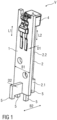
- the figures 1 and 2 and 5 to 7 show schematic representations of a printed circuit board assembly V made up of two printed circuit boards 1, 2 that are connected to one another at least in a form-fitting manner.
- the first printed circuit board 1 carries at least one component 4, in particular an electronic component 4.
- this component 4 is designed as a sensor, so that this first printed circuit board 1 is designed as a sensor carrier printed circuit board.
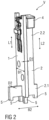
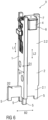
- the second circuit board 2 is designed as a support circuit board, the function of which is to support the first circuit board 1, in particular during a connection process described below for connecting at least the first circuit board 1 to an in figure 4 illustrated third circuit board 3, for example a main circuit board, to the circuit board assembly V, which then includes these three circuit boards 1, 2, 3.
- This connection process during which the second printed circuit board 2 supports the first printed circuit board 1, so that in particular it is ensured that the first printed circuit board 1 does not change its position relative to the third printed circuit board 3, includes, for example, an assembly process, a soldering process and/or a plastic encapsulation process, in particular with a thermoset plastic.
- the second circuit board 2 one or more components 4, in particular carry electronic components 4 and/or electrical conductor tracks, as does the first printed circuit board 1.
- the printed circuit board assembly V can be used, for example, in a vehicle, for example in a control unit of the vehicle, for example in a transmission control unit.
- a control unit of the vehicle for example in a transmission control unit.
- other possible uses are also conceivable, in particular in electrical or electronic devices which have a plurality of printed circuit boards connected to one another.
- the printed circuit board assembly V which comprises at least the first printed circuit board 1 and the second printed circuit board 2 and expediently also, as in figure 4 shown, also includes the third printed circuit board 3, the first printed circuit board 1 and the second printed circuit board 2 are at least positively connected to one another. This is advantageously done using what is known as a two-groove connection.
- the first printed circuit board 1 and the second printed circuit board 2 each have at least one groove N1, N2.
- the first printed circuit board 1 and the second printed circuit board 2 are, as in figure 3 shown connected to each other in such a way that the bottoms of the two grooves N1, N2 touch.
- the connection of the first printed circuit board 1 and the second printed circuit board 2 is in figure 3 using the example in the figures 1 and 2 shown first circuit board 1 and second circuit board 2 shown. Joining the in the Figures 5 to 7 illustrated embodiments of the first and second printed circuit board 1, 2 is essentially in the same way.
- the first printed circuit board 1 and the second printed circuit board 2 are plate-shaped and therefore each have two opposite flat sides, two longitudinal sides and two transverse sides. The long sides and transverse sides essentially form a peripheral side edge of the respective printed circuit board 1, 2.
- the first printed circuit board 1 and the second printed circuit board 2 are essentially elongated, ie they each have a length dimension L1, L2, a width dimension B1, B2 and a Thickness dimension D1, D2, wherein the length dimension L1, L2 is larger, in particular significantly larger, than the width dimension B1, B2 and wherein the width dimension B1, B2 is larger, in particular significantly larger, than the thickness dimension D1, D2.
- the long sides are longer than the short sides of the respective printed circuit board 1, 2.
- Longitudinal extension L1, L2 means an extension of the respective printed circuit board 1, 2 in its longitudinal direction.
- the width extension B1, B2 is to be understood as meaning an extension of the respective printed circuit board 1, 2 in its transverse direction, ie width direction.
- Thickness expansion D1, D2 is to be understood as meaning an expansion of the respective printed circuit board 1, 2 in its thickness direction.
- the respective groove N1, N2 is designed as a depression in the respective side edge.
- a groove depth direction thus runs from an upper edge of the groove, i. H. from a slot opening to the slot bottom of the respective slot N1, N2.
- a groove direction of the respective groove N1, N2 runs at right angles to the groove depth direction and thus from one flat side to the opposite flat side of the respective printed circuit board 1, 2.
- the groove N1 in the first printed circuit board 1 is formed in the area of one of the transverse sides, with the direction of the groove depth extending in the direction of the other transverse side, i.e. in the direction of the longitudinal extent L1 of the first printed circuit board 1.
- the groove N1 is formed in the region of the transverse side facing away from the component 4 arranged on the first printed circuit board 1. This lateral side, in which the groove N1 is formed, is provided for connection to the third printed circuit board 3.
- the second circuit board 2 has in the embodiments according to Figures 1 to 4 6 and 7 has a wide area 2.1 and an adjoining narrow area 2.2, with a width extension B2 of the wide area 2.1 being greater than a width extension B2 of the narrow area 2.2.
- the wide area 2.1 extends to a transverse side of the second printed circuit board 2, which is provided for connection to the third printed circuit board 3.
- support feet can be provided which are placed on a flat side of the third circuit board 3 .
- the groove N2 is formed in the second circuit board 2 in an edge side of the wide area 2.1, which faces the transverse side of the second circuit board 2 associated with the narrow area 2.2.
- the direction of the groove depth runs in the direction of the length L2 of the second circuit board 2, with the groove bottom being arranged closer to the transverse side associated with the wide area 2.1 and the groove edge consequently being arranged closer to the transverse side associated with the narrow area 2.2.
- One of the groove walls is designed as an extension of a longitudinal edge area of the narrow area 2.2 into the wide area 2.1.
- the side walls of the slot N1 in the first printed circuit board 1 lie on one flat side of the second printed circuit board 2 and the side walls of the slot N2 in the second printed circuit board 2 lie on one flat side of the first one Printed circuit board 1, so that the printed circuit boards 1, 2 are conveniently clamped together via the grooves N1, N2.
- the narrow area 2.2 of the second printed circuit board 2 rests against one flat side of the first printed circuit board 1 over a significant part of the length L1 of the first printed circuit board 1, in particular over more than half of the length L1 of the first printed circuit board 1, and thus supports the first printed circuit board 1, in particular against tilting.
- the first printed circuit board 1 and the second printed circuit board 1 are thus connected to one another or are connected to one another in the finished printed circuit board assembly V in such a way that flat sides of the first printed circuit board 1 are aligned at right angles to flat sides of the second printed circuit board 2, i. H. Surface normals of the first and second printed circuit board 1, 2 are aligned at right angles to one another.
- the length extensions L1, L2, in particular their respective direction, of the two printed circuit boards 1, 2 are aligned parallel to one another.
- the groove extension directions of the two grooves N1, N2 are aligned at right angles to one another and the groove depth directions of the two grooves N1, N2 are aligned parallel to one another.
- Corresponding shaping of the second printed circuit board 2 also makes it possible for at least one component 4, in particular the sensor, to be supported on the first printed circuit board 1 by the second printed circuit board 2, in order thereby to achieve improved positioning accuracy of this component 4.
- this is achieved in that the length dimension L2 of the second printed circuit board 2 is designed in such a way that the second printed circuit board 2 when assembled with the first printed circuit board 1 extends up to the component 4 to be supported on the first printed circuit board 1, i.e. rests against the component 4 to be supported.
- the second printed circuit board 2 is designed in such a way that it encloses the component 4 to be supported at least in regions when it is assembled with the first printed circuit board 1 .
- the The second circuit board 2 has a component recess 6 corresponding to a component shape of the component 4 to be supported, in which the component 4 to be supported is arranged after the joining of the first and second circuit boards 1, 2 and is thereby supported by the second circuit board 2 in several directions, in particular from above and below, i.e. in the direction of length extension of the first circuit board 1.
- this enables the position of the component 4, for example the sensor, to be secured in the plastic encapsulation process.
- the second printed circuit board 2 has a latching lug 7 with which it snaps into place on the component 4 .
- a plurality of components 4 can also be supported on the first circuit board 1 by means of the second circuit board 2, given a corresponding shaping of the second circuit board 2 .
- a correspondingly adapted shape of the second printed circuit board 2 enables support for differently designed components 4, for example for different sensor construction concepts.
- the shape of the second printed circuit board 2 must be adapted to the design of the respective component 4 .
- the first circuit board 1 is designed in such a way as already mentioned above Figures 1 to 4 and 6 and 7 described.
- the second printed circuit board 2 is significantly shorter; it essentially only includes the wide area 2.1 of the second printed circuit board 2 according to the other exemplary embodiments.
- the groove N2 is formed here in the area of one long side, with the groove depth direction extending in the direction of the other long side, i.e. in the direction of the width extension B2 of the second circuit board 2.
- the groove N2 is formed in the area of the long side, which is not intended for connection to the third circuit board 3.
- the other long side, which is designed to be connected to the third printed circuit board 3 is, in this embodiment the second printed circuit board 2 has the two positioning formations 5 or feet in the width extent B2 of the second printed circuit board 2 .
- the first and second printed circuit boards 1, 2 are advantageously connected to one another via the two-groove connector, as shown in FIG figure 3 shown, and then the first and second printed circuit boards 1, 2 are connected to the third printed circuit board 3, as in FIG figure 4 shown.
- the first printed circuit board 1 is held in position on the third printed circuit board 3 by its positioning formations 5, i.e. the positioning pins, expediently in the area of soldering points on the third printed circuit board 3. This positioning is carried out here by clamping the positioning formations 5 in the respective corresponding recess in the third printed circuit board 3.
- the second printed circuit board 2 can first be arranged on the third printed circuit board 3 and then the first printed circuit board 1 in the manner described in the second printed circuit board 2, if present, with its respective positioning formation 5 are inserted into the respective corresponding recess in the third printed circuit board 3.
- the positioning formations 5 of the first and/or second printed circuit board 1, 2 can be metallically coated at least in certain areas, advantageously circumferentially, and soldered into the third printed circuit board 3, expediently without electrical contacting. This is called the principle of blind contact soldering. This soldering of the first and/or second printed circuit board 1, 2 to the third printed circuit board 3 thus only serves to secure the position of the first and/or second printed circuit board 1, 2 relative to the third printed circuit board 3.
- the first printed circuit board 1 is arranged vertically on the second printed circuit board 3, with its length extension L1 parallel to a normal vector of the third printed circuit board 3, i.e. to the normal vector of the flat side of the third printed circuit board 3.
- the component 4 for example the sensor, is arranged on the first printed circuit board 1 at a distance from the third printed circuit board.
- the first printed circuit board 1 is populated after, d. H. after connection to the third printed circuit board 3 in the manner described above and/or after the first and/or third printed circuit board 1, 3 has been fitted with further components 4, in a plastic overmolding tool, in particular in a duroplastic injection molding tool. It is there expediently in the x-direction, i. H. in the direction of thickness extension, and in the y-direction, i. H. in the direction of width expansion, held in the plastic overmoulding tool. The z-direction, i. H. the direction of linear expansion, is expediently left free, d. H. in this direction, the first circuit board 1 is not in contact with an inside of the plastic encapsulation tool, so that no compressive forces act on the third circuit board 3 and soldering points.
- the first printed circuit board 1 is now overmolded with a plastic, in particular with a thermosetting plastic, at least in certain areas or completely.
- the second printed circuit board 2 is also encapsulated in areas or completely and/or at least areas of the third printed circuit board 3 are overmoulded with the plastic, in particular duroplast.
- the component 4 is designed as a sensor on the first printed circuit board 1, a so-called sensor dome is realized by this printed circuit board assembly V.
- the sensor is arranged at a distance from the third printed circuit board 3, which is expediently designed as the main printed circuit board that it can protrude, for example, from a control unit housing and into another unit, for example into a transmission of a vehicle, protrudes or is at least arranged on a housing or in a housing recess of the housing of the other unit.
- the first printed circuit board 1 and the second printed circuit board 2 expediently have one or more corresponding latching formations.
- the first printed circuit board 1 and the second printed circuit board 2 expediently have one or more corresponding latching formations.
- a corresponding printed circuit board latching lug 8 is formed, which snaps into place in the latching opening when the two printed circuit boards 1, 2 are joined together.
- corresponding snap-in hooks can be provided on the first and second printed circuit boards 1, 2, which are pushed into one another and snap into place when the first and second printed circuit boards 1, 2 are joined together. This latching achieves greater stability during the plastic encapsulation and, for example, also during use of the circuit board assembly V.
- support geometries can also be provided on one or more of the printed circuit boards 1, 2, 3, in particular on the first and/or second printed circuit board 1, 2, and/or in the plastic injection molding tool. i.e. appropriate support and/or mount formations.
- the printed circuit board assembly V produced in the manner described thus includes, as shown in FIG figures 1 and 2 5 to 7, at least the first printed circuit board 1 and the second printed circuit board 2, which are connected in the manner described, in particular by two-groove plugging, at least in a form-fitting manner, for example also in a force-fitting manner.
- the printed circuit board assembly V produced in the manner described expediently comprises the first, second and third printed circuit boards 1, 2, 3, with at least the first printed circuit board 1 and the second printed circuit board 2 being connected in the manner described, in particular by means of a two-groove connection, at least in a form-fitting manner, for example also in a force-fitting manner.
- the first and/or second printed circuit board 1, 2 are connected to the third printed circuit board 3, for example, in a form-fitting, force-fitting and/or cohesive manner, cohesively in particular through the plastic, in particular duroplastic, due to the plastic encapsulation described above, and/or, for example, by soldering.
- the positive connection of the first and/or second printed circuit board 1, 2 to the third printed circuit board 3 is achieved, for example, by one or more positioning formations 5 introduced into respective recesses in the third printed circuit board 3.
- the form fit between the first and second circuit board 1, 2 can also result from the latching described above.
- the printed circuit board assembly V can be used, for example, in a transmission control unit for a vehicle or in another control unit or in another electrical device.
- the first printed circuit board 1 is expediently designed as a sensor carrier printed circuit board and carries the sensor as a component 4 .
- the second printed circuit board 2 is designed as a support printed circuit board and the third printed circuit board 3 as a main printed circuit board.
- the arrangement of the first printed circuit board 1 supported by the second printed circuit board 2 on the third printed circuit board 3 forms a so-called sensor dome.
Landscapes
- Engineering & Computer Science (AREA)
- Microelectronics & Electronic Packaging (AREA)
- Manufacturing & Machinery (AREA)
- Combinations Of Printed Boards (AREA)
- Structure Of Printed Boards (AREA)
Description
- Die Erfindung betrifft einen Leiterplattenverbund und ein Verfahren zu dessen Herstellung.
- Aus dem Stand der Technik sind Leiterplatten allgemein bekannt.
-
US 4 513 064 A ,DE 10 2012 213304 A1 ,US 2013/003331 A1 undDE 42 44 626 A1 offenbaren Leiterplattenverbunde nach dem Stand der Technik. - Der Erfindung liegt die Aufgabe zugrunde, ein gegenüber dem Stand der Technik verbessertes Verfahren zur Herstellung eines Leiterplattenverbundes und einen gegenüber dem Stand der Technik verbesserten Leiterplattenverbund anzugeben.
- Die Aufgabe wird erfindungsgemäß gelöst durch ein Verfahren zur Herstellung eines Leiterplattenverbundes mit den Merkmalen des Anspruchs 1 und einen Leiterplattenverbund mit den Merkmalen des Anspruchs 6.
- Vorteilhafte Ausgestaltungen der Erfindung sind Gegenstand der Unteransprüche.
- In einem erfindungsgemäßen Verfahren zur Herstellung eines Leiterplattenverbundes wird eine erste Leiterplatte, insbesondere eine Sensorträgerleiterplatte, mit einer zweiten Leiterplatte, insbesondere einer Stützleiterplatte, formschlüssig verbunden. Dadurch wird ein Stützen der ersten Leiterplatte durch die zweite Leiterplatte insbesondere während eines Verbindungsprozesses der ersten Leiterplatte und der zweiten Leiterplatte mit einer insbesondere als Hauptleiterplatte ausgebildeten dritten Leiterplatte erreicht. Dieser Verbindungsprozess umfasst beispielsweise das Anordnen der ersten und zweiten Leiterplatte auf der dritten Leiterplatte und das bereichsweise oder vollständige Umspritzen zumindest der ersten Leiterplatte mit einem Kunststoff, insbesondere mit einem Duroplastkunsstoff, in einem Kunststoffumspritzprozess, in welchem zumindest die erste und zweckmäßigerweise auch die zweite Leiterplatte in einem Kunststoffspritzwerkzeug angeordnet und mit Kunststoff umspritzt werden.
- Erfindungsgemäß weisen beide Leiterplatten jeweils eine Nut auf, wobei die beiden Leiterplatten derart miteinander verbunden werden, dass sich Nutböden der beiden Nuten berühren. Die beiden Leiterplatten werden somit derart zusammengefügt, dass sich deren Nuten ineinanderschieben, so dass Nutseitenwände der ersten Leiterplatte an Flachseiten der zweiten Leiterplatte anliegen und Nutseitenwände der zweiten Leiterplatte an Flachseiten der ersten Leiterplatte anliegen. Diese Verbindung wird auch als Zweinutverbindung bezeichnet. Zweckmäßigerweise wird dadurch ein Verklemmen der jeweiligen Leiterplatte in der Nut der jeweiligen anderen Leiterplatte erreicht, so dass nicht nur eine formschlüssige, sondern auch eine kraftschlüssige Verbindung erreicht wird.
- Erfindungsgemäß werden die beiden Leiterplatten derart zueinander ausgerichtet verbunden, dass Flächennormalen der beiden Leiterplatten rechtwinklig zueinander ausgerichtet sind.
- Erfindungsgemäß verlaufen Längenausdehnungen der beiden Leiterplatten dabei parallel zueinander. Zweckmäßigerweise sind die Längenausdehnungen der beiden Leiterplatten im Wesentlichen gleich groß und die beiden Leiterplatten liegen im Wesentlichen über ihren Längenausdehnungsbereich aneinander an oder die zweite Leiterplatte liegt über einen wesentlichen Längenausdehnungsbereich der ersten Leiterplatte, insbesondere über mehr als die Hälfte des Längenausdehnungsbereichs der ersten Leiterplatte, an der ersten Leiterplatte an. Zweckmäßigerweise sind die erste und zweite Leiterplatte derart ausgebildet und werden derart miteinander verbunden, dass die erste Leiterplatte über ihren gesamten Längenausdehnungsbereich oder über einen wesentlichen Teil davon, insbesondere über mehr als die Hälfte des Längenausdehnungsbereichs, von der zweiten Leiterplatte gestützt wird.
- Erfindungsgemäß werden die beiden Leiterplatten derart miteinander verbunden, dass ein auf der ersten Leiterplatte angeordnetes Bauelement, insbesondere ein Sensor, durch die zweite Leiterplatte in seiner Position gestützt wird. Hierzu liegt die zweite Leiterplatte nach dem Verbinden der beiden Leiterplatten zweckmäßigerweise am Bauelement an, insbesondere an zumindest einer Umfangsseite des Bauelements oder an mehreren Umfangsseiten. Beispielsweise wird die zweite Leiterplatte am Sensor verrastet. Auf diese Weise wird das Bauelement auf der ersten Leiterplatte durch die zweite Leiterplatte gestützt und in Position gehalten, zum Beispiel während des Kunststoffumspritzprozesses. Durch eine entsprechende Formgebung der zweiten Leiterplatte ist eine Stützung für verschiedene Bauelementaufbaukonzepte, beispielsweise Sensoraufbaukonzepte, möglich. Durch diese Stützung des Bauelements, beispielsweise des Sensors, wird insbesondere eine verbesserte Positioniergenauigkeit erreicht.
- Vorteilhafterweise kann vorgesehen sein, dass die beiden Leiterplatten miteinander verrastet werden. Beispielsweise weisen die beiden Leiterplatten korrespondierende Rasthaken oder andere korrespondierende Rastelemente auf. Beispielsweise weist eine der Leiterplatten eine oder mehrere Rastnasen und die andere Leiterplatte eine zur jeweiligen Rastnase korrespondierende Rastöffnung auf. Dadurch wird ein Auseinanderdriften der beiden Leiterplatten, insbesondere während des Kunststoffumspritzprozesses, vermieden.
- Zweckmäßigerweise wird zumindest die erste Leiterplatte mit der dritten Leiterplatte, insbesondere der Hauptleiterplatte, verbunden. Dadurch wird beispielsweise ein so genannter Sensordom ausgebildet, wenn das Bauelement auf der ersten Leiterplatte als ein Sensor ausgebildet ist. Dabei steht die erste Leiterplatte zweckmäßigerweise senkrecht auf der dritten Leiterplatte.
- In einer vorteilhaften Ausführungsform wird zumindest eine Positionierausformung der ersten Leiterplatte in eine korrespondierende Ausnehmung in der dritten Leiterplatte eingeführt. Dadurch wird eine Position der ersten Leiterplatte relativ zur dritten Leiterplatte, insbesondere relativ zu Lötstellen auf der dritten Leiterplatte, gesichert.
- Es kann vorgesehen sein, dass die erste Leiterplatte und die dritte Leiterplatte miteinander verlötet werden. Beispielsweise ist hierzu die zumindest eine Positionierausformung zumindest bereichsweise, zweckmäßigerweise umlaufend, metallisch beschichtet. Zweckmäßigerweise erfolgt das Verlöten ohne elektrische Kontaktführung, d. h. über diese Verlötung ist später keine Stromführung vorgesehen. Dies wird auch als Prinzip der Blindkontaktverlötung bezeichnet.
- Zweckmäßigerweise wird zumindest die erste Leiterplatte mit einem Kunststoff, insbesondere mit einem Duroplastkunststoff, zumindest bereichsweise umspritzt. Vorzugsweise werden auch die zweite Leiterplatte zumindest bereichsweise und/oder zumindest ein Bereich der dritten Leiterplatte mit dem Kunststoff umspritzt. Dadurch wird eine stoffschlüssige Verbindung der ersten Leiterplatte mit der zweiten und/oder dritten Leiterplatte erreicht.
- Im Folgenden werden nochmals vorteilhafte Ausführungsformen des Verfahrens zur Herstellung des Leiterplattenverbundes beschrieben. Der mittels des beschriebenen Verfahrens hergestellte Leiterplattenverbund kann beispielsweise in einem Fahrzeug verwendet werden, beispielsweise in einem Getriebesteuergerät. Dabei ist die erste Leiterplatte zweckmäßigerweise als Sensorträgerleiterplatte ausgebildet, welche als Bauelement den Sensor trägt, und die dritte Leiterplatte ist als Hauptleiterplatte ausgebildet. Ein Fügeprozess zum Verbinden der ersten und zweiten Leiterplatte erfolgt zweckmäßigerweise, wie bereits beschrieben, über die so genannte Zweinutsteckung. Die als Stützleiterplatte ausgebildete zweite Leiterplatte hat die Funktion, die zweckmäßigerweise als Sensorträgerleiterplatte ausgebildete erste Leiterplatte in einem nachfolgenden Montageprozess, Lötprozess und/oder Kunststoffumspritzprozess, insbesondere Duroplastumspritzprozess, zu stützen.
- Die mit einem oder mehreren beispielsweise jeweils als Sensor ausgebildeten Bauelementen bestückte und zweckmäßigerweise als Sensorträgerleiterplatte ausgebildete erste Leiterplatte wird zweckmäßigerweise bezüglich der dritten Leiterplatte in Position gehalten über eine oder mehrere Positionierausformungen, auch als Positionierpins bezeichnet. Sie wird zweckmäßigerweise im Bereich von Lötstellen in der dritten Leiterplatte in Position gehalten. Die Positionierung kann erfolgen durch Klemmung in entsprechenden Ausnehmungen, beispielsweise Aufnahmebohrungen in der dritten Leiterplatte. In anderen Ausführungsformen können an der dritten Leiterplatte eine oder mehrere Positionierausformungen und in der ersten Leiterplatte eine jeweilige korrespondierende Ausnehmung vorgesehen sein.
- Des Weiteren kann die jeweilige Positionierausformung umlaufend metallisch beschichtet sein und ohne elektrische Kontaktführung eingelötet werden (Prinzip der Blindkontaktverlötung). Zweckmäßigerweise wird die erste Leiterplatte, insbesondere Sensorträgerleiterplatte, vorzugsweise nach dem Bestücken, in einem Kunststoffumspritzungsprozess, insbesondere Duroplastumspritzungsprozess in einem entsprechenden Werkzeug aufgenommen und in x-Richtung und y-Richtung, d. h. in Breitenausdehnungsrichtung und Dickenausdehnungsrichtung aufgenommen. Die Z- Richtung, d. h. die Längenausdehnungsrichtung, bleibt frei, um keine Druckkräfte auf die beispielsweise als Hauptleiterplatte ausgebildete dritte Leiterplatte und die Lötstellen zu erhalten.
- Durch eine weitere Formgebung der als Stützleiterplatte ausgebildeten zweiten Leiterplatte kann das Bauelement, beispielsweise der Sensor, auf der ersten Leiterplatte gestützt werden, um eine verbesserte Positioniergenauigkeit des Bauelements, insbesondere des Sensors, zu erhalten. Hier ist eine Unterstützung für unterschiedliche Bauelementaufbaukonzepte, insbesondere Sensoraufbaukonzepte, möglich. Auch kann das Bauelement, insbesondere der Sensor, durch eine Ausnehmung in der als Stützleiterplatte ausgebildeten zweiten Leiterplatte von oben und unten genauer in Position gehalten werden im Kunststoffumspritzungsprozess.
- Um ein Auseinanderdriften der ersten und zweiten Leiterplatte insbesondere im oberen Bereich zu vermeiden, können Verrastungen, beispielsweise Rasthaken, vorgesehen sein, die im Zusammenfügungsprozess der ersten und zweiten Leiterplatte ineinander eingeschoben werden und somit noch mehr Stabilität beispielsweise im oben bereits erwähnten Sensordomkonzept ermöglichen.
- Nach dem Zusammenfügen der drei Leiterplatten kann das Sensordomkonzept mit Kunststoff, insbesondere Duroplast, umspritzt werden. Dabei wird insbesondere die erste Leiterplatte zumindest bereichsweise umspritzt. Durch abgestimmte Supportgeometrien kann die Position insbesondere der ersten Leiterplatte mit dem Bauelement im Umspritzungswerkzeug während des Umspritzungsvorganges genauer gehalten werden.
- Ein erfindungsgemäßer Leiterplattenverbund, welcher insbesondere mittels des oben beschriebenen Verfahrens hergestellt ist, umfasst mindestens zwei formschlüssig miteinander verbundene Leiterplatten. Dabei wird durch die zweite Leiterplatte die Stützung der ersten Leiterplatte erreicht, insbesondere für nachfolgende Bearbeitungsprozesse und/oder einen Einsatz des Leiterplattenverbundes in einem Gerät, beispielsweise in einem Steuergerät eines Fahrzeugs, zum Beispiel in einem Getriebesteuergerät.
- Zweckmäßigerweise umfasst der Leiterplattenverbund drei miteinander verbundene Leiterplatten, vorzugsweise die als Sensorträgerleiterplatte ausgebildete erste Leiterplatte, zu deren Stützung die als Stützleiterplatte ausgebildete zweite Leiterplatte und die als Hauptleiterplatte ausgebildete dritte Leiterplatte.
- Die erste und zweite Leiterplatte sind formschlüssig miteinander verbunden, insbesondere über die Zweinutsteckung, und können zudem kraftschlüssig und/oder stoffschlüssig verbunden sein, stoffschlüssig beispielsweise durch das Kunststoffumspritzen.
- Die dritte Leiterplatte ist mit der ersten und/oder zweiten Leiterplatte formschlüssig, kraftschlüssig und/oder stoffschlüssig verbunden, beispielsweise verlötet, durch das Kunststoffumspritzen und/oder durch das Einfügen und beispielsweise verklemmen einer oder mehrerer Positionierausformungen in einer jeweiligen korrespondierenden Ausnehmung. Die erste Leiterplatte ist im Wesentlichen senkrecht zur dritten Leiterplatte ausgerichtet. Dadurch wird, wenn das Bauelement auf der ersten Leiterplatte als ein Sensor ausgebildet ist, ein Sensordom erreicht, mittels welchem der Sensor von der zweckmäßigerweise als Hauptleiterplatte ausgebildeten dritten Leiterplatte beabstandet ist.
- Ausführungsbeispiele der Erfindung werden im Folgenden anhand von Zeichnungen näher erläutert.
- Dabei zeigen:
- Figur 1
- schematisch eine perspektivische Darstellung einer Ausführungsform eines Leiterplattenverbundes aus zwei Leiterplatten,
- Figur 2
- schematisch eine weitere perspektivische Darstellung der Ausführungsform des Leiterplattenverbundes aus
Figur 1 , - Figur 3
- schematisch eine Montage des Leiterplattenverbundes aus den
Figuren 1 und2 , - Figur 4
- schematisch eine perspektivische Darstellung eines Leiterplattenverbundes aus drei Leiterplatten,
- Figur 5
- schematisch eine perspektivische Darstellung einer Ausführungsform eines Leiterplattenverbundes aus zwei Leiterplatten außerhalb des Schutzumfangs der Ansprüche,
- Figur 6
- schematisch eine perspektivische Darstellung einer weiteren Ausführungsform eines Leiterplattenverbundes aus zwei Leiterplatten, und
- Figur 7
- schematisch eine weitere perspektivische Darstellung der Ausführungsform des Leiterplattenverbundes aus
Figur 6 . - Einander entsprechende Teile sind in allen Figuren mit den gleichen Bezugszeichen versehen.
- Die
Figuren 1 und2 sowie 5 bis 7 zeigen schematische Darstellungen eines Leiterplattenverbundes V aus zwei zumindest formschlüssig miteinander verbundenen Leiterplatten 1, 2. Dabei trägt die erste Leiterplatte 1 zumindest ein Bauelement 4, insbesondere ein elektronisches Bauelement 4. Im dargestellten Beispiel ist dieses Bauelement 4 als ein Sensor ausgebildet, so dass diese erste Leiterplatte 1 als eine Sensorträgerleiterplatte ausgebildet ist. - Die zweite Leiterplatte 2 ist als eine Stützleiterplatte ausgebildet, deren Funktion es ist, die erste Leiterplatte 1 zu stützen, insbesondere während eines im Folgenden beschriebenen Verbindungsprozesses zum Verbinden zumindest der ersten Leiterplatte 1 mit einer in
Figur 4 dargestellten dritten Leiterplatte 3, beispielsweise einer Hauptleiterplatte, zum Leiterplattenverbund V, welcher dann diese drei Leiterplatten 1, 2, 3 umfasst. Dieser Verbindungsprozess, während dessen die zweite Leiterplatte 2 die erste Leiterplatte 1 stützt, so dass insbesondere sichergestellt wird, dass die erste Leiterplatte 1 ihre Position relativ zur dritten Leiterplatte 3 nicht verändert, umfasst beispielsweise einen Montageprozess, einen Lötprozess und/oder einen Kunststoffumspritzprozess, insbesondere mit einem duroplastischen Kunststoff. - Zusätzlich zu dieser Stützfunktion kann beispielsweise auch die zweite Leiterplatte 2 ein oder mehrere Bauelemente 4, insbesondere elektronische Bauelemente 4, und/oder elektrische Leiterzüge tragen, ebenso wie die erste Leiterplatte 1.
- Der Leiterplattenverbund V kann beispielsweise in einem Fahrzeug verwendet werden, zum Beispiel in einem Steuergerät des Fahrzeugs, beispielsweise in einem Getriebesteuergerät. Es sind jedoch auch andere Einsatzmöglichkeiten denkbar, insbesondere in elektrischen oder elektronischen Geräten, welche mehrere miteinander verbundene Leiterplatten aufweisen.
- In einem Verfahren zur Herstellung des Leiterplattenverbundes V, welcher zumindest die erste Leiterplatte 1 und die zweite Leiterplatte 2 umfasst und zweckmäßigerweise des Weiteren, wie in
Figur 4 gezeigt, auch die dritte Leiterplatte 3 umfasst, werden die erste Leiterplatte 1 und die zweite Leiterplatte 2 zumindest formschlüssig miteinander verbunden. Dies erfolgt vorteilhafterweise über eine so genannte Zweinutsteckung. - Um dies zu ermöglichen, weisen die erste Leiterplatte 1 und die zweite Leiterplatte 2 jeweils zumindest eine Nut N1, N2 auf. Die erste Leiterplatte 1 und die zweite Leiterplatte 2 werden, wie in
Figur 3 gezeigt, derart miteinander verbunden, dass sich Nutböden der beiden Nuten N1, N2 berühren. Das Verbinden der ersten Leiterplatte 1 und zweiten Leiterplatte 2 ist inFigur 3 am Beispiel der in denFiguren 1 und2 dargestellten ersten Leiterplatte 1 und zweiten Leiterplatte 2 gezeigt. Das Verbinden der in denFiguren 5 bis 7 dargestellten Ausführungsformen der ersten und zweiten Leiterplatte 1, 2 erfolgt im Wesentlichen auf die gleiche Weise. - Die erste Leiterplatte 1 und die zweite Leiterplatte 2 sind plattenförmig ausgebildet und weisen daher jeweils zwei gegenüberliegende Flachseiten, zwei Längsseiten und zwei Querseiten auf. Die Längsseiten und Querseiten bilden im Wesentlichen einen umlaufenden Seitenrand der jeweiligen Leiterplatte 1, 2. Die erste Leiterplatte 1 und die zweite Leiterplatte 2 sind im Wesentlichen länglich ausgebildet, d. h. sie weisen jeweils eine Längenausdehnung L1, L2, eine Breitenausdehnung B1, B2 und eine Dickenausdehnung D1, D2 auf, wobei die Längenausdehnung L1, L2 größer ist, insbesondere wesentlich größer ist, als die Breitenausdehnung B1, B2 und wobei die Breitenausdehnung B1, B2 größer ist, insbesondere wesentlich größer ist, als die Dickenausdehnung D1, D2. Entsprechend der Längsausdehnung L1, L2 und Breitenausdehnung B1, B2 sind die Längsseiten länger als die Querseiten der jeweiligen Leiterplatte 1, 2. Unter Längenausdehnung L1, L2 ist eine Ausdehnung der jeweiligen Leiterplatte 1, 2 in ihrer Längsrichtung zu verstehen. Unter Breitenausdehnung B1, B2 ist eine Ausdehnung der jeweiligen Leiterplatte 1, 2 in ihrer Querrichtung, d. h. Breitenrichtung, zu verstehen. Unter Dickenausdehnung D1, D2 ist eine Ausdehnung der jeweiligen Leiterplatte 1, 2 in ihrer Dickenrichtung zu verstehen.
- Die jeweilige Nut N1, N2 ist als eine Vertiefung im jeweiligen Seitenrand ausgebildet. Eine Nuttiefenrichtung verläuft somit von einem oberen Nutrand, d. h. von einer Nutöffnung, zum Nutboden der jeweiligen Nut N1, N2. Eine Nutverlaufsrichtung der jeweiligen Nut N1, N2 verläuft rechtwinklig zur Nuttiefenrichtung und somit von einer Flachseite zur gegenüberliegenden Flachseite der jeweiligen Leiterplatte 1, 2.
- Die Nut N1 in der ersten Leiterplatte 1 ist im Bereich einer der Querseiten ausgebildet, wobei sich die Nuttiefenrichtung in Richtung der anderen Querseite erstreckt, d. h. in Richtung der Längenausdehnung L1 der ersten Leiterplatte 1. Insbesondere ist die Nut N1 im Bereich der vom auf der ersten Leiterplatte 1 angeordneten Bauelement 4 abgewandten Querseite ausgebildet. Diese Querseite, in welcher die Nut N1 ausgebildet ist, ist zur Verbindung mit der dritten Leiterplatte 3 vorgesehen. Sie weist daher in den dargestellten Ausführungsbeispielen gemäß den
Figuren 1 bis 7 beidseits der Nut N1 jeweils eine Positionierausformung 5, auch als Positionierpins bezeichnet, in Längenausdehnung L1 der ersten Leiterplatte 1 auf, welche zur Montage der ersten Leiterplatte 1 mit der dritten Leiterplatte 3 in eine jeweilige korrespondierende Ausnehmung, beispielsweise eine Aufnahmebohrung, in der dritten Leiterplatte 3 eingeführt wird. - Die zweite Leiterplatte 2 weist in den Ausführungsbeispielen gemäß den
Figuren 1 bis 4 sowie 6 und 7 einen breiten Bereich 2.1 und einen anschließenden schmalen Bereich 2.2 auf, wobei eine Breitenausdehnung B2 des breiten Bereichs 2.1 größer ist als eine Breitenausdehnung B2 des schmalen Bereichs 2.2. Der breite Bereich 2.1 erstreckt sich bis zu einer Querseite der zweiten Leiterplatte 2, welche zur Verbindung mit der dritten Leiterplatte 3 vorgesehen ist. Sie weist daher zweckmäßigerweise ebenfalls zwei Positionierausformungen 5, auch als Positionierpins bezeichnet, in Längenausdehnung L2 der zweiten Leiterplatte 2 auf, welche zur Montage der zweiten Leiterplatte 2 mit der dritten Leiterplatte 3 in eine jeweilige korrespondierende Ausnehmung, beispielsweise Aufnahmebohrung, in der dritten Leiterplatte 3 eingeführt werden. Alternativ können anstelle der Positionierausformungen 5 Stützfüße vorgesehen sein, welche auf eine Flachseite der dritten Leiterplatte 3 aufsetzen. - Die Nut N2 ist in der zweiten Leiterplatte 2 in einer Randseite des breiten Bereichs 2.1 ausgebildet, welche der dem schmalen Bereich 2.2 zugeordneten Querseite der zweiten Leiterplatte 2 zugewandt ist. Die Nuttiefenrichtung verläuft dabei in Richtung der Längenausdehnung L2 der zweiten Leiterplatte 2, wobei der Nutboden näher an der dem breiten Bereich 2.1 zugeordneten Querseite und der Nutrand demzufolge näher an der dem schmalen Bereich 2.2 zugeordneten Querseite angeordnet ist. Eine der Nutwände ist dabei als eine Verlängerung eines Längsrandbereichs des schmalen Bereichs 2.2 in den breiten Bereich 2.1 hinein ausgebildet.
- Werden die erste Leiterplatte 1 und die zweite Leiterplatte 2 auf die in
Figur 3 gezeigte Weise über die Zweinutsteckung miteinander verbunden, liegen Nutseitenwände der Nut N1 in der ersten Leiterplatte 1 an jeweils einer Flachseite der zweiten Leiterplatte 2 an und Nutseitenwände der Nut N2 in der zweiten Leiterplatte 2 liegen an jeweils einer Flachseite der ersten Leiterplatte 1 an, so dass die Leiterplatten 1, 2 über die Nuten N1, N2 zweckmäßigerweise miteinander verklemmt sind. Zudem liegt der schmale Bereich 2.2 der zweiten Leiterplatte 2 über einen wesentlichen Teil der Längenausdehnung L1 der ersten Leiterplatte 1, insbesondere über mehr als die Hälfte der Längenausdehnung L1 der ersten Leiterplatte 1, an der einen Flachseite der ersten Leiterplatte 1 an und stützt somit die erste Leiterplatte 1 insbesondere gegen ein Verkippen ab. - Die erste Leiterplatte 1 und die zweite Leiterplatte 1 werden somit derart miteinander verbunden oder sind im fertiggestellten Leiterplattenverbund V derart miteinander verbunden, dass Flachseiten der ersten Leiterplatte 1 rechtwinklig zu Flachseiten der zweiten Leiterplatte 2 ausgerichtet sind, d. h. Flächennormalen der ersten und zweiten Leiterplatte 1, 2 sind rechtwinklig zueinander ausgerichtet. Dabei sind die Längenausdehnungen L1, L2, insbesondere deren jeweilige Richtung, der beiden Leiterplatten 1, 2 parallel zueinander ausgerichtet. Die Nutverlaufsrichtungen der beiden Nuten N1, N2 sind dabei rechtwinklig zueinander ausgerichtet und die Nuttiefenrichtungen der beiden Nuten N1, N2 sind parallel zueinander ausgerichtet.
- Durch eine entsprechende Ausformung der zweiten Leiterplatte 2 wird es zudem ermöglicht, dass zumindest eine Bauelement 4, insbesondere den Sensor, auf der ersten Leiterplatte 1 durch die zweite Leiterplatte 2 zu stützen, um dadurch eine verbesserte Positioniergenauigkeit dieses Bauelements 4 zu erhalten. In den Ausführungsbeispielen gemäß den
Figuren 1 bis 4 wird dies dadurch erreicht, dass die Längenausdehnung L2 der zweiten Leiterplatte 2 derart ausgebildet ist, dass sich die zweite Leiterplatte 2 im mit der ersten Leiterplatte 1 zusammengefügten Zustand bis an das zu stützende Bauelement 4 auf der ersten Leiterplatte 1 heran erstreckt, d. h. am zu stützenden Bauelement 4 anliegt. In den Ausführungsbeispielen gemäß denFiguren 6 und7 wird dies dadurch erreicht, dass die zweite Leiterplatte 2 derart ausgebildet ist, dass sie im mit der ersten Leiterplatte 1 zusammengefügten Zustand das zu stützende Bauelement 4 zumindest bereichsweise umschließt. D. h. die zweite Leiterplatte 2 weist eine mit einer Bauelementform des zu stützenden Bauelements 4 korrespondierende Bauelementausnehmung 6 auf, in welcher das zu stützende Bauelement 4 nach dem Zusammenfügen der ersten und zweiten Leiterplatte 1, 2 angeordnet ist und dadurch in mehrere Richtungen, insbesondere von oben und unten, d. h. in Längenausdehnungsrichtung der ersten Leiterplatte 1, durch die zweite Leiterplatte 2 gestützt ist. Dies ermöglicht insbesondere eine Positionssicherung des Bauelements 4, beispielsweise des Sensors, im Kunststoffumspritzprozess. Beispielsweise weist die zweite Leiterplatte 2 eine Rastnase 7 auf, mit welcher sie am Bauelement 4 einrastet. Auf die beschriebene Weise können mittels der zweiten Leiterplatte 2, bei entsprechender Ausformung der zweiten Leiterplatte 2, auch mehrere Bauelemente 4 auf der ersten Leiterplatte 1 gestützt werden. - Durch eine entsprechend angepasste Formgebung der zweiten Leiterplatte 2 ist eine Stützung für unterschiedlich ausgebildete Bauelemente 4, beispielsweise für unterschiedliche Sensoraufbaukonzepte, möglich. Die Formgebung der zweiten Leiterplatte 2 ist hierzu an die Ausbildung des jeweiligen Bauelements 4 anzupassen.
- In einem Ausführungsbeispiel außerhalb des Schutzumfangs der Ansprüche gemäß
Figur 5 ist die erste Leiterplatte 1 derart ausgebildet, wie bereits oben zu denFiguren 1 bis 4 sowie 6 und 7 beschrieben. Die zweite Leiterplatte 2 ist jedoch wesentlich kürzer, sie umfasst im Wesentlichen lediglich den breiten Bereich 2.1 der zweiten Leiterplatte 2 gemäß den anderen Ausführungsbeispielen. - Daher ist hier die Nut N2 im Bereich einer Längsseite ausgebildet, wobei sich die Nuttiefenrichtung in Richtung der anderen Längsseite erstreckt, d. h. in Richtung der Breitenausdehnung B2 der zweiten Leiterplatte 2. Die Nut N2 ist dabei im Bereich der Längsseite ausgebildet, welche nicht zur Verbindung mit der dritten Leiterplatte 3 vorgesehen ist. Die andere Längsseite, welche zur Verbindung mit der dritten Leiterplatte 3 ausgebildet ist, weist bei dieser Ausführungsform der zweiten Leiterplatte 2 die beiden Positionierausformungen 5 oder Füße in Breitenausdehnung B2 der zweiten Leiterplatte 2 auf.
- Zur Montage des Leiterplattenverbundes V, welcher zweckmäßigerweise die erste, zweite und dritte Leiterplatte 1, 2, 3 umfasst, werden somit vorteilhafterweise die erste und zweite Leiterplatte 1, 2 über die Zweinutsteckung miteinander verbunden, wie in
Figur 3 gezeigt, und anschließend werden die erste und zweite Leiterplatte 1, 2 mit der dritten Leiterplatte 3 verbunden, wie inFigur 4 gezeigt. Dabei wird die erste Leiterplatte 1 über ihre Positionierausformungen 5, d. h. die Positionierpins, auf der dritten Leiterplatte 3 in Position gehalten, zweckmäßigerweise im Bereich von Lötstellen auf der dritten Leiterplatte 3. Diese Positionierung erfolgt hier durch Klemmung der Positionierausformungen 5 in der jeweiligen korrespondierenden Ausnehmung in der dritten Leiterplatte 3. Alternativ kann auch zunächst die zweite Leiterplatte 2 auf der dritten Leiterplatte 3 angeordnet werden und danach die erste Leiterplatte 1 auf die beschriebene Weise in die zweite Leiterplatte 2, wenn vorhanden, mit ihrer jeweiligen Positionierungsausformung 5 in die jeweilige korrespondierende Ausnehmung in der dritten Leiterplatte 3 eingeschoben werden. - Dies gilt zweckmäßigerweise auch für die zweite Leiterplatte 2 und deren Positionierausformungen 5, falls diese vorhanden sind. Die Positionierausformungen 5 der ersten und/oder zweiten Leiterplatte 1, 2 können zumindest bereichsweise, vorteilhafterweise umlaufend, metallisch beschichtet sein und, zweckmäßigerweise ohne elektrische Kontaktführung, in die dritte Leiterplatte 3 eingelötet werden. Dies wird als Prinzip der Blindkontaktverlötung bezeichnet. Dieses Verlöten der ersten und/oder zweiten Leiterplatte 1, 2 mit der dritten Leiterplatte 3 dient somit lediglich der Positionssicherung der ersten und/oder zweiten Leiterplatte 1, 2 relativ zur dritten Leiterplatte 3.
- Wie in
Figur 4 gezeigt, ist nach diesem Zusammenfügen der drei Leiterplatten 1, 2, 3 die erste Leiterplatte 1 senkrecht auf der zweiten Leiterplatte 3 angeordnet, wobei ihre Längenausdehnung L1 parallel zu einem Normalenvektor der dritten Leiterplatte 3, d. h. zum Normalenvektor der Flachseite der dritten Leiterplatte 3, verläuft. Dadurch ist das Bauelement 4, beispielsweise der Sensor, auf der ersten Leiterplatte 1 mittels dieser von der dritten Leiterplatte beabstandet angeordnet. - Zweckmäßigerweise wird die erste Leiterplatte 1 nach dem bestücken, d. h. nach dem Verbinden mit der dritten Leiterplatte 3 auf die oben beschriebene Weise und/oder nach einem Bestücken der ersten und/oder dritten Leiterplatte 1, 3 mit weiteren Bauelementen 4, in einem Kunststoffumspritzwerkzeug, insbesondere in einem Duroplastumspritzwerkzeug, aufgenommen. Sie wird dort zweckmäßigerweise in x-Richtung, d. h. in Dickenausdehnungsrichtung, und in y-Richtung, d. h. in Breitenausdehnungsrichtung, im Kunststoffumspritzwerkzeug gehalten. Die z-Richtung, d. h. die Längenausdehnungsrichtung, bleibt zweckmäßigerweise frei, d. h. in dieser Richtung liegt die erste Leiterplatte 1 nicht an einer Innenseite des Kunststoff- umspritzwerkzeugs an, damit keine Druckkräfte auf die dritte Leiterplatte 3 und auf Lötstellen einwirken.
- Zur Vollendung der Herstellung des Leiterplattenverbundes V aus erster, zweiter und dritter Leiterplatte 1, 2, 3 wird nun die erste Leiterplatte 1 mit einem Kunststoff, insbesondere mit einen Duroplastkunststoff, zumindest bereichsweise oder vollständig umspritzt. Zweckmäßigerweise werden dabei auch die zweite Leiterplatte 2 bereichsweise oder vollständig und/oder zumindest Bereiche der dritten Leiterplatte 3 mit dem Kunststoff, insbesondere Duroplast, umspritzt.
- Ist das Bauelement 4 auf der ersten Leiterplatte 1 als ein Sensor ausgebildet, wird durch diesen Leiterplattenverbund V ein so genannter Sensordom realisiert. Bei einem Sensordom ist der Sensor von der zweckmäßigerweise als Hauptleiterplatte ausgebildeten dritten Leiterplatte 3 beabstandet angeordnet, so dass er zum Beispiel aus einem Steuergerätgehäuse herausragen kann und in eine andere Einheit, beispielsweise in ein Getriebe eines Fahrzeugs, hineinragt oder zumindest an einem Gehäuse oder in einer Gehäuseausnehmung des Gehäuses der anderen Einheit angeordnet ist.
- Um, insbesondere während des Kunststoffumspritzens, ein Auseinanderdriften der ersten und zweiten Leiterplatte 1, 2 insbesondere im von der dritten Leiterplatte 3 abgewandten Bereich zu vermeiden, kann vorgesehen sein, dass die erste Leiterplatte 1 und die zweite Leiterplatte 2 miteinander verrastet werden, wie beispielsweise in
Figur 7 gezeigt. Hierzu weisen die erste Leiterplatte 1 und die zweite Leiterplatte 2 zweckmäßigerweise eine oder mehrere korrespondierende Rastausformungen auf. Beispielsweise ist in einer der beiden Leiterplatten 1, 2, inFigur 7 in der ersten Leiterplatte 1, zumindest eine Rastöffnung ausgebildet und an der anderen Leiterplatte 2, 1, inFigur 7 an der zweiten Leiterplatte 2, ist eine korrespondierende Leiterplattenrastnase 8 ausgebildet, welche durch das Zusammenfügen der beiden Leiterplatten 1, 2 in die Rastöffnung einrastet. In anderen Ausführungsformen können korrespondierende Rasthaken an der ersten und zweiten Leiterplatte 1, 2 vorgesehen sein, welche durch das Zusammenfügen der ersten und zweiten Leiterplatte 1, 2 ineinander eingeschoben werden und einrasten. Durch diese Verrastung wird eine größere Stabilität während des Kunststoffumspritzens und beispielsweise auch während eines Einsatzes des Leiterplattenverbundes V erreicht. - Um eine Positionshaltung der Leiterplatten 1, 2, 3 zueinander und/oder des zumindest einen Bauelements 4 auf der ersten Leiterplatte 1 insbesondere im Kunststoffspritzgusswerkzeug zusätzlich zu verbessern, können zudem so genannte Supportgeometrien an einer oder mehrerer der Leiterplatten 1, 2, 3, insbesondere an der ersten und/oder zweiten Leiterplatte 1, 2, und/oder im Kunststoffspritzgusswerkzeug vorgesehen sein. D. h. entsprechende Stützungs- und/oder Halterungsausformungen.
- Der auf die beschriebene Weise hergestellte Leiterplattenverbund V umfasst somit, wie in den
Figuren 1 und2 sowie 5 bis 7 gezeigt, zumindest die erste Leiterplatte 1 und die zweite Leiterplatte 2, welche auf die beschriebene Weise, insbesondere durch Zweinutsteckung, zumindest formschlüssig verbunden sind, beispielsweise zudem auch kraftschlüssig. Zweckmäßigerweise umfasst der auf die beschriebene Weise hergestellte Leiterplattenverbund V die erste, zweite und dritte Leiterplatte 1, 2, 3, wobei zumindest die erste Leiterplatte 1 und die zweite Leiterplatte 2 auf die beschriebene Weise, insbesondere durch Zweinutsteckung, zumindest formschlüssig, beispielsweise zudem auch kraftschlüssig, verbunden sind. - Die erste und/oder zweite Leiterplatte 1, 2 sind mit der dritten Leiterplatte 3 beispielsweise formschlüssig, kraftschlüssig und/oder stoffschlüssig verbunden, stoffschlüssig insbesondere durch den Kunststoff, insbesondere Duroplastkunststoff, aufgrund des oben beschriebenen Kunststoffumspritzens, und/oder beispielsweise durch Verlöten. Die formschlüssige Verbindung der ersten und/oder zweiten Leiterplatte 1, 2 mit der dritten Leiterplatte 3 wird beispielsweise durch einen oder mehrere in jeweilige Ausnehmungen der dritten Leiterplatte 3 eingeführte Positionierausformungen 5 erreicht. Der Formschluss zwischen erster und zweiter Leiterplatte 1, 2 kann zudem aus der oben beschriebenen Verrastung resultieren.
- Der Leiterplattenverbund V kann beispielsweise in einem Getriebesteuergerät für ein Fahrzeug oder in einem anderen Steuergerät oder in einem anderen elektrischen Gerät verwendet werden. Insbesondere bei einer Verwendung im Getriebesteuergerät ist die erste Leiterplatte 1 zweckmäßigerweise als eine Sensorträgerleiterplatte ausgebildet und trägt als Bauelement 4 den Sensor. Die zweite Leiterplatte 2 ist als Stützleiterplatte und die dritte Leiterplatte 3 als Hauptleiterplatte ausgebildet. Durch die Anordnung der durch die zweite Leiterplatte 2 gestützten ersten Leiterplatte 1 auf der dritten Leiterplatte 3 ist ein so genannter Sensordom ausgebildet.
-
- 1
- erste Leiterplatte
- 2
- zweite Leiterplatte
- 2.1
- breiter Bereich
- 2.2
- schmaler Bereich
- 3
- dritte Leiterplatte
- 4
- Bauelement
- 5
- Positionierausformung
- 6
- Bauelementausnehmung
- 7
- Rastnase
- 8
- Leiterplattenrastnase
- B1, B2
- Breitenausdehnung
- D1, D2
- Dickenausdehnung
- L1, L2
- Längenausdehnung
- N1, N2
- Nut
- V
- Leiterplattenverbund
Claims (7)
- Verfahren zur Herstellung eines Leiterplattenverbundes (V), wobei eine erste Leiterplatte (1), insbesondere eine Sensorträgerleiterplatte, mit einer zweiten Leiterplatte (2), insbesondere einer Stützleiterplatte, formschlüssig verbunden wird, wobei die Längenausdehnungen (L1, L2) der beiden Leiterplatten (1, 2) parallel zueinander ausgerichtet sind, wobei beide Leiterplatten (1, 2) jeweils eine Nut (N1, N2) aufweisen und wobei die beiden Leiterplatten (1, 2) derart miteinander verbunden werden, dass sich Nutböden der beiden Nuten (N1, N2) berühren, wobei die beiden Leiterplatten (1, 2) derart zueinander ausgerichtet verbunden werden, dass Flächennormalen der beiden Leiterplatten (1, 2) rechtwinklig zueinander ausgerichtet sind,
dadurch gekennzeichnet, dassdie Nut (N1) im Bereich der von einem auf der ersten Leiterplatte (1) angeordneten Bauelement (4) abgewandten Querseite ausgebildet ist,die zweite Leiterplatte (2) einen breiten Bereich (2.1) und einen anschließenden schmalen Bereich (2.2) aufweist, wobei der schmale Bereich (2.2) über einen wesentlichen Teil der Längenausdehnung (L1) der ersten Leiterplatte (1) liegt, und die Nut (N2)in der zweiten Leiterplatte (2) in einer Randseite des breiten Bereichs (2.1) ausgebildet ist, und dassdie Leiterplatten (1, 2) derart miteinander verbunden werden, dass das auf der ersten Leiterplatte (1) angeordnete Bauelement (4), insbesondere Sensor, durch die zweite Leiterplatte (2) in seiner Position gestützt wird. - Verfahren nach Anspruch 1,
wobei die beiden Leiterplatten (1, 2) miteinander verrastet werden. - Verfahren nach einem der vorhergehenden Ansprüche,
wobei zumindest die erste Leiterplatte (1) mit einer dritten Leiterplatte (3) verbunden wird. - Verfahren nach einem der vorhergehenden Ansprüche,
wobei zumindest eine Positionierausformung (5) der ersten Leiterplatte (1) in eine korrespondierende Ausnehmung in der dritten Leiterplatte (3) eingeführt wird und/oder die erste Leiterplatte (1) und die dritte Leiterplatte (3) miteinander verlötet werden. - Verfahren nach einem der vorhergehenden Ansprüche,
wobei zumindest die erste Leiterplatte (1) mit einem Kunststoff zumindest bereichsweise umspritzt wird. - Leiterplattenverbund (V), insbesondere hergestellt mittels eines Verfahrens nach einem der vorhergehenden Ansprüche, umfassend mindestens zwei formschlüssig miteinander verbundene Leiterplatten (1, 2), wobei eine erste Leiterplatte (1), insbesondere eine Sensorträgerleiterplatte, mit einer zweiten Leiterplatte (2), insbesondere einer Stützleiterplatte, formschlüssig verbunden ist, wobei die Längenausdehnungen (L1, L2) der beiden Leiterplatten (1, 2) parallel zueinander ausgerichtet sind, wobei beide Leiterplatten (1, 2) jeweils eine Nut (N1, N2) aufweisen und wobei die beiden Leiterplatten (1, 2) derart miteinander verbunden sind, dass sich Nutböden der beiden Nuten (N1, N2) berühren, wobei die beiden Leiterplatten (1, 2) derart zueinander ausgerichtet verbunden sind, dass Flächennormalen der beiden Leiterplatten (1, 2) rechtwinklig zueinander ausgerichtet sind,
dadurch gekennzeichnet, dass die Nut (N1) im Bereich der von einem auf der ersten Leiterplatte (1) angeordneten Bauelement (4) abgewandten Querseite ausgebildet ist, die zweite Leiterplatte (2) einen breiten Bereich (2.1) und einen anschließenden schmalen Bereich (2.2) aufweist, wobei der schmale Bereich (2.2) über einen wesentlichen Teil der Längenausdehnung (L1) der ersten Leiterplatte (1) liegt, und die Nut (N2) in der zweiten Leiterplatte (2) in einer Randseite des breiten Bereichs (2.1) ausgebildet ist, und dass die Leiterplatten (1, 2) derart miteinander verbunden sind, dass das auf der ersten Leiterplatte (1) angeordnete Bauelement (4), insbesondere Sensor, durch die zweite Leiterplatte (2) in seiner Position gestützt ist. - Leiterplattenverbund (V) nach Anspruch 6, umfassend drei miteinander verbundene Leiterplatten (1, 2, 3).
Applications Claiming Priority (2)
| Application Number | Priority Date | Filing Date | Title |
|---|---|---|---|
| DE102016224653.4A DE102016224653B4 (de) | 2016-12-12 | 2016-12-12 | Leiterplattenverbund und Verfahren zu dessen Herstellung |
| PCT/EP2017/082109 WO2018108758A1 (de) | 2016-12-12 | 2017-12-08 | Leiterplattenverbund und verfahren zu dessen herstellung |
Publications (2)
| Publication Number | Publication Date |
|---|---|
| EP3552463A1 EP3552463A1 (de) | 2019-10-16 |
| EP3552463B1 true EP3552463B1 (de) | 2023-07-26 |
Family
ID=60702710
Family Applications (1)
| Application Number | Title | Priority Date | Filing Date |
|---|---|---|---|
| EP17816673.2A Active EP3552463B1 (de) | 2016-12-12 | 2017-12-08 | Leiterplattenverbund und verfahren zu dessen herstellung |
Country Status (7)
| Country | Link |
|---|---|
| US (1) | US10893615B2 (de) |
| EP (1) | EP3552463B1 (de) |
| JP (1) | JP6828164B2 (de) |
| KR (1) | KR102423939B1 (de) |
| CN (1) | CN110169212B (de) |
| DE (1) | DE102016224653B4 (de) |
| WO (1) | WO2018108758A1 (de) |
Families Citing this family (7)
| Publication number | Priority date | Publication date | Assignee | Title |
|---|---|---|---|---|
| KR102622914B1 (ko) * | 2017-02-06 | 2024-01-10 | 삼성전자주식회사 | 전력 공급 장치 및 전력 공급 장치를 포함하는 전자 장치 |
| JP1663818S (de) * | 2018-12-26 | 2020-07-20 | ||
| USD936025S1 (en) * | 2018-12-26 | 2021-11-16 | Lg Chem, Ltd. | Flexible printed circuit board for battery module |
| TWD202895S (zh) * | 2019-03-27 | 2020-02-21 | 家登精密工業股份有限公司 | 光罩盒組裝件 |
| CN114498117B (zh) * | 2020-10-23 | 2024-06-18 | 台达电子工业股份有限公司 | 插座结构 |
| EP4509411A1 (de) | 2023-08-16 | 2025-02-19 | Goodrich Lighting Systems GmbH & Co. KG | Flugzeugleuchte, flugzeug mit einer flugzeugleuchte und verfahren zur montage einer flugzeugleuchte |
| DE102024200130B3 (de) | 2024-01-05 | 2025-03-20 | Vitesco Technologies Germany Gmbh | Elektronikbaugruppe und Verfahren zur Herstellung der Elektronikbaugruppe |
Family Cites Families (24)
| Publication number | Priority date | Publication date | Assignee | Title |
|---|---|---|---|---|
| US2958013A (en) * | 1956-08-20 | 1960-10-25 | Arthur Ansley Mfg Co | Electrical unit |
| US3522485A (en) * | 1967-11-21 | 1970-08-04 | Automatic Radio Mfg Co | Modular circuit construction |
| DE2441209A1 (de) | 1974-08-28 | 1976-03-11 | Erie Elektronik Gmbh | Elektrische anschlusskontaktierung |
| US4513064A (en) * | 1982-12-17 | 1985-04-23 | The United States Of America As Represented By The Secretary Of The Army | Package for rugged electronics |
| JPS6251769U (de) * | 1985-09-18 | 1987-03-31 | ||
| DE3919273C2 (de) | 1989-06-13 | 1993-10-14 | Bosch Gmbh Robert | Leiterplattenanordnung |
| DE4244626C2 (de) * | 1992-12-29 | 1995-02-09 | Mannesmann Ag | Anordnung zum Positionieren |
| JPH1154875A (ja) * | 1997-07-31 | 1999-02-26 | Nec Home Electron Ltd | プリント基板の保持構造 |
| US20020071259A1 (en) | 2000-11-13 | 2002-06-13 | Sture Roos | Circuit board assembly |
| SE0004161D0 (sv) * | 2000-11-13 | 2000-11-13 | Ericsson Telefon Ab L M | Circuit board assembly |
| US6804120B2 (en) * | 2001-12-18 | 2004-10-12 | Siemens Vdo Automotive Corporation | Method and apparatus for connecting circuit boards for a sensor assembly |
| JP2008071848A (ja) * | 2006-09-13 | 2008-03-27 | Funai Electric Co Ltd | テレビジョン受像機用回路基板ユニット及び電子機器用回路基板ユニット |
| US7435095B1 (en) * | 2007-06-11 | 2008-10-14 | Hon Hai Precision Ind. Co., Ltd. | Electrical interconnection system |
| US7864544B2 (en) * | 2007-08-01 | 2011-01-04 | Delphi Technologies, Inc. | Printed circuit board assembly |
| JP2009152331A (ja) * | 2007-12-20 | 2009-07-09 | Panasonic Corp | 配線基板の加工方法、および半導体装置 |
| US8328571B2 (en) * | 2010-11-04 | 2012-12-11 | Tyco Electronics Corporation | Connector assemblies having moveable mating arrays and power connectors |
| CH704882A2 (fr) * | 2011-04-29 | 2012-10-31 | Fischer Connectors Holding Sa | Connecteur haute densité. |
| CN102858088A (zh) | 2011-06-28 | 2013-01-02 | 鸿富锦精密工业(深圳)有限公司 | 电路板及其制作方法及采用该电路板的电子产品 |
| GB2494919B (en) * | 2011-09-23 | 2015-06-17 | Control Tech Ltd | Method for connecting printed circuit boards. |
| TWI456379B (zh) * | 2012-07-23 | 2014-10-11 | Chicony Power Tech Co Ltd | 電源系統及其組合式電源裝置 |
| DE102012213304A1 (de) * | 2012-07-30 | 2014-01-30 | Zf Friedrichshafen Ag | Verfahren zum Herstellen einer dreidimensionalen Leiterplattenanordnung und dreidimensionale Leiterplattenanordnung |
| US9163792B2 (en) | 2013-07-23 | 2015-10-20 | Zacaabel, Llc | Illuminated hand wand |
| US9108262B1 (en) * | 2014-04-17 | 2015-08-18 | Topline Corporation | Disposable apparatus for aligning and dispensing solder columns in an array |
| DE102016224657A1 (de) * | 2016-12-12 | 2018-06-14 | Conti Temic Microelectronic Gmbh | Verfahren zum Verbinden eines Bauelementträgers mit einer Leiterplatte und Verbund aus einer Leiterplatte und einem Bauelementträger |
-
2016
- 2016-12-12 DE DE102016224653.4A patent/DE102016224653B4/de not_active Expired - Fee Related
-
2017
- 2017-12-08 KR KR1020197018382A patent/KR102423939B1/ko active Active
- 2017-12-08 EP EP17816673.2A patent/EP3552463B1/de active Active
- 2017-12-08 US US16/468,820 patent/US10893615B2/en active Active
- 2017-12-08 JP JP2019531276A patent/JP6828164B2/ja active Active
- 2017-12-08 CN CN201780071642.2A patent/CN110169212B/zh active Active
- 2017-12-08 WO PCT/EP2017/082109 patent/WO2018108758A1/de not_active Ceased
Also Published As
| Publication number | Publication date |
|---|---|
| JP2020501377A (ja) | 2020-01-16 |
| KR20190087565A (ko) | 2019-07-24 |
| DE102016224653B4 (de) | 2022-07-21 |
| US20200077525A1 (en) | 2020-03-05 |
| WO2018108758A1 (de) | 2018-06-21 |
| DE102016224653A1 (de) | 2018-06-14 |
| KR102423939B1 (ko) | 2022-07-21 |
| CN110169212B (zh) | 2023-01-20 |
| CN110169212A (zh) | 2019-08-23 |
| EP3552463A1 (de) | 2019-10-16 |
| US10893615B2 (en) | 2021-01-12 |
| JP6828164B2 (ja) | 2021-02-10 |
Similar Documents
| Publication | Publication Date | Title |
|---|---|---|
| EP3552463B1 (de) | Leiterplattenverbund und verfahren zu dessen herstellung | |
| DE69816882T2 (de) | Verfahren zum Herstellen eines Verbinders und ein Verbinder hergestellt durch Formen mit Einsetzung und dessen Verwendung | |
| DE112017007139B4 (de) | Gehäuse, elektronische Vorrichtung und Verfahren zur Herstellung eines Gehäuses | |
| EP0982978B1 (de) | Gehäuse, insbesondere Schlossgehäuse mit elektrischen Anschlusseinrichtungen | |
| WO2013178212A2 (de) | Kraftfahrzeug-komponententräger und verfahren zu seiner herstellung | |
| DE102013209435A1 (de) | Steckerverbindung mit einem zur Vermeidung von Spänen optimierten Führungselement | |
| DE10260241B4 (de) | Kontaktierungsbauteil und Verfahren zur Herstellung eines Kontaktierungsbauteils | |
| DE102010034975A1 (de) | Elektronische Schaltung | |
| DE102016119057B4 (de) | Sensorelement für einen kapazitiven Sensor und Verfahren zur Herstellung des Sensorelements und des Sensors | |
| DE102012105352A1 (de) | Positionierelement | |
| DE102014216518A1 (de) | Elektronische Steuereinheit sowie Moldwerkzeug und Verfahren zum Herstellen einer elektronischen Steuereinheit | |
| DE102005039086B4 (de) | Verfahren zum Herstellen einer elektrischen Verbindungseinrichtung sowie derart hergestellte Verbindungseinrichtung | |
| DE10345632B4 (de) | Anordnung mit einem Sensor | |
| DE102018206480B4 (de) | Verbinder und Steuergerät | |
| DE102016224657A1 (de) | Verfahren zum Verbinden eines Bauelementträgers mit einer Leiterplatte und Verbund aus einer Leiterplatte und einem Bauelementträger | |
| DE102017011113B4 (de) | Elektrisches Verbindungselement mit einer Stromschiene | |
| DE102014204051A1 (de) | Verbindungsanordnung, Verfahren zum Herstellen einer Verbindungsanordnung und elektrisches Gerät mit einer Verbindungsanordnung | |
| WO2019038285A1 (de) | Sensorbauteil, vormontageanordnung für ein sensorbauteil und verfahren zur herstellung eines sensorbauteils | |
| LU101641B1 (de) | System aus einem Steckkontaktträger und wenigstens einem Steckkontaktelement , Steckkontaktträger, Steckkontaktelement und Steckverbinder | |
| DE10306618A1 (de) | Planare Kontaktstruktur mit Kontaktzungen für eine variable Steckposition | |
| DE102007002749B3 (de) | Modularer Steckeraufbau | |
| DE102023201588A1 (de) | Elektronikmodul | |
| DE19841467A1 (de) | Platinen-Steckkontakt-Anordnung | |
| DE102024113214A1 (de) | Kontaktelement und Steckverbinder | |
| DE102016219662A1 (de) | Gehäuse zur Aufnahme einer ein- oder mehrteiligen Leiterplatte |
Legal Events
| Date | Code | Title | Description |
|---|---|---|---|
| STAA | Information on the status of an ep patent application or granted ep patent |
Free format text: STATUS: UNKNOWN |
|
| STAA | Information on the status of an ep patent application or granted ep patent |
Free format text: STATUS: THE INTERNATIONAL PUBLICATION HAS BEEN MADE |
|
| PUAI | Public reference made under article 153(3) epc to a published international application that has entered the european phase |
Free format text: ORIGINAL CODE: 0009012 |
|
| STAA | Information on the status of an ep patent application or granted ep patent |
Free format text: STATUS: REQUEST FOR EXAMINATION WAS MADE |
|
| 17P | Request for examination filed |
Effective date: 20190524 |
|
| AK | Designated contracting states |
Kind code of ref document: A1 Designated state(s): AL AT BE BG CH CY CZ DE DK EE ES FI FR GB GR HR HU IE IS IT LI LT LU LV MC MK MT NL NO PL PT RO RS SE SI SK SM TR |
|
| AX | Request for extension of the european patent |
Extension state: BA ME |
|
| RAP1 | Party data changed (applicant data changed or rights of an application transferred) |
Owner name: VITESCO TECHNOLOGIES GERMANY GMBH |
|
| DAV | Request for validation of the european patent (deleted) | ||
| DAX | Request for extension of the european patent (deleted) | ||
| STAA | Information on the status of an ep patent application or granted ep patent |
Free format text: STATUS: EXAMINATION IS IN PROGRESS |
|
| 17Q | First examination report despatched |
Effective date: 20210407 |
|
| RAP3 | Party data changed (applicant data changed or rights of an application transferred) |
Owner name: VITESCO TECHNOLOGIES GERMANY GMBH |
|
| GRAP | Despatch of communication of intention to grant a patent |
Free format text: ORIGINAL CODE: EPIDOSNIGR1 |
|
| STAA | Information on the status of an ep patent application or granted ep patent |
Free format text: STATUS: GRANT OF PATENT IS INTENDED |
|
| INTG | Intention to grant announced |
Effective date: 20230329 |
|
| GRAS | Grant fee paid |
Free format text: ORIGINAL CODE: EPIDOSNIGR3 |
|
| GRAA | (expected) grant |
Free format text: ORIGINAL CODE: 0009210 |
|
| STAA | Information on the status of an ep patent application or granted ep patent |
Free format text: STATUS: THE PATENT HAS BEEN GRANTED |
|
| P01 | Opt-out of the competence of the unified patent court (upc) registered |
Effective date: 20230530 |
|
| AK | Designated contracting states |
Kind code of ref document: B1 Designated state(s): AL AT BE BG CH CY CZ DE DK EE ES FI FR GB GR HR HU IE IS IT LI LT LU LV MC MK MT NL NO PL PT RO RS SE SI SK SM TR |
|
| REG | Reference to a national code |
Ref country code: CH Ref legal event code: EP |
|
| REG | Reference to a national code |
Ref country code: DE Ref legal event code: R096 Ref document number: 502017015118 Country of ref document: DE |
|
| REG | Reference to a national code |
Ref country code: IE Ref legal event code: FG4D Free format text: LANGUAGE OF EP DOCUMENT: GERMAN |
|
| REG | Reference to a national code |
Ref country code: LT Ref legal event code: MG9D |
|
| REG | Reference to a national code |
Ref country code: NL Ref legal event code: MP Effective date: 20230726 |
|
| PG25 | Lapsed in a contracting state [announced via postgrant information from national office to epo] |
Ref country code: NL Free format text: LAPSE BECAUSE OF FAILURE TO SUBMIT A TRANSLATION OF THE DESCRIPTION OR TO PAY THE FEE WITHIN THE PRESCRIBED TIME-LIMIT Effective date: 20230726 |
|
| PG25 | Lapsed in a contracting state [announced via postgrant information from national office to epo] |
Ref country code: GR Free format text: LAPSE BECAUSE OF FAILURE TO SUBMIT A TRANSLATION OF THE DESCRIPTION OR TO PAY THE FEE WITHIN THE PRESCRIBED TIME-LIMIT Effective date: 20231027 |
|
| PG25 | Lapsed in a contracting state [announced via postgrant information from national office to epo] |
Ref country code: IS Free format text: LAPSE BECAUSE OF FAILURE TO SUBMIT A TRANSLATION OF THE DESCRIPTION OR TO PAY THE FEE WITHIN THE PRESCRIBED TIME-LIMIT Effective date: 20231126 |
|
| PG25 | Lapsed in a contracting state [announced via postgrant information from national office to epo] |
Ref country code: SE Free format text: LAPSE BECAUSE OF FAILURE TO SUBMIT A TRANSLATION OF THE DESCRIPTION OR TO PAY THE FEE WITHIN THE PRESCRIBED TIME-LIMIT Effective date: 20230726 Ref country code: RS Free format text: LAPSE BECAUSE OF FAILURE TO SUBMIT A TRANSLATION OF THE DESCRIPTION OR TO PAY THE FEE WITHIN THE PRESCRIBED TIME-LIMIT Effective date: 20230726 Ref country code: PT Free format text: LAPSE BECAUSE OF FAILURE TO SUBMIT A TRANSLATION OF THE DESCRIPTION OR TO PAY THE FEE WITHIN THE PRESCRIBED TIME-LIMIT Effective date: 20231127 Ref country code: NO Free format text: LAPSE BECAUSE OF FAILURE TO SUBMIT A TRANSLATION OF THE DESCRIPTION OR TO PAY THE FEE WITHIN THE PRESCRIBED TIME-LIMIT Effective date: 20231026 Ref country code: LV Free format text: LAPSE BECAUSE OF FAILURE TO SUBMIT A TRANSLATION OF THE DESCRIPTION OR TO PAY THE FEE WITHIN THE PRESCRIBED TIME-LIMIT Effective date: 20230726 Ref country code: LT Free format text: LAPSE BECAUSE OF FAILURE TO SUBMIT A TRANSLATION OF THE DESCRIPTION OR TO PAY THE FEE WITHIN THE PRESCRIBED TIME-LIMIT Effective date: 20230726 Ref country code: IS Free format text: LAPSE BECAUSE OF FAILURE TO SUBMIT A TRANSLATION OF THE DESCRIPTION OR TO PAY THE FEE WITHIN THE PRESCRIBED TIME-LIMIT Effective date: 20231126 Ref country code: HR Free format text: LAPSE BECAUSE OF FAILURE TO SUBMIT A TRANSLATION OF THE DESCRIPTION OR TO PAY THE FEE WITHIN THE PRESCRIBED TIME-LIMIT Effective date: 20230726 Ref country code: GR Free format text: LAPSE BECAUSE OF FAILURE TO SUBMIT A TRANSLATION OF THE DESCRIPTION OR TO PAY THE FEE WITHIN THE PRESCRIBED TIME-LIMIT Effective date: 20231027 Ref country code: FI Free format text: LAPSE BECAUSE OF FAILURE TO SUBMIT A TRANSLATION OF THE DESCRIPTION OR TO PAY THE FEE WITHIN THE PRESCRIBED TIME-LIMIT Effective date: 20230726 |
|
| PG25 | Lapsed in a contracting state [announced via postgrant information from national office to epo] |
Ref country code: PL Free format text: LAPSE BECAUSE OF FAILURE TO SUBMIT A TRANSLATION OF THE DESCRIPTION OR TO PAY THE FEE WITHIN THE PRESCRIBED TIME-LIMIT Effective date: 20230726 |
|
| PG25 | Lapsed in a contracting state [announced via postgrant information from national office to epo] |
Ref country code: ES Free format text: LAPSE BECAUSE OF FAILURE TO SUBMIT A TRANSLATION OF THE DESCRIPTION OR TO PAY THE FEE WITHIN THE PRESCRIBED TIME-LIMIT Effective date: 20230726 |
|
| REG | Reference to a national code |
Ref country code: DE Ref legal event code: R097 Ref document number: 502017015118 Country of ref document: DE |
|
| PG25 | Lapsed in a contracting state [announced via postgrant information from national office to epo] |
Ref country code: SM Free format text: LAPSE BECAUSE OF FAILURE TO SUBMIT A TRANSLATION OF THE DESCRIPTION OR TO PAY THE FEE WITHIN THE PRESCRIBED TIME-LIMIT Effective date: 20230726 Ref country code: RO Free format text: LAPSE BECAUSE OF FAILURE TO SUBMIT A TRANSLATION OF THE DESCRIPTION OR TO PAY THE FEE WITHIN THE PRESCRIBED TIME-LIMIT Effective date: 20230726 Ref country code: ES Free format text: LAPSE BECAUSE OF FAILURE TO SUBMIT A TRANSLATION OF THE DESCRIPTION OR TO PAY THE FEE WITHIN THE PRESCRIBED TIME-LIMIT Effective date: 20230726 Ref country code: EE Free format text: LAPSE BECAUSE OF FAILURE TO SUBMIT A TRANSLATION OF THE DESCRIPTION OR TO PAY THE FEE WITHIN THE PRESCRIBED TIME-LIMIT Effective date: 20230726 Ref country code: DK Free format text: LAPSE BECAUSE OF FAILURE TO SUBMIT A TRANSLATION OF THE DESCRIPTION OR TO PAY THE FEE WITHIN THE PRESCRIBED TIME-LIMIT Effective date: 20230726 Ref country code: CZ Free format text: LAPSE BECAUSE OF FAILURE TO SUBMIT A TRANSLATION OF THE DESCRIPTION OR TO PAY THE FEE WITHIN THE PRESCRIBED TIME-LIMIT Effective date: 20230726 Ref country code: SK Free format text: LAPSE BECAUSE OF FAILURE TO SUBMIT A TRANSLATION OF THE DESCRIPTION OR TO PAY THE FEE WITHIN THE PRESCRIBED TIME-LIMIT Effective date: 20230726 |
|
| PG25 | Lapsed in a contracting state [announced via postgrant information from national office to epo] |
Ref country code: IT Free format text: LAPSE BECAUSE OF FAILURE TO SUBMIT A TRANSLATION OF THE DESCRIPTION OR TO PAY THE FEE WITHIN THE PRESCRIBED TIME-LIMIT Effective date: 20230726 |
|
| PLBE | No opposition filed within time limit |
Free format text: ORIGINAL CODE: 0009261 |
|
| STAA | Information on the status of an ep patent application or granted ep patent |
Free format text: STATUS: NO OPPOSITION FILED WITHIN TIME LIMIT |
|
| 26N | No opposition filed |
Effective date: 20240429 |
|
| PG25 | Lapsed in a contracting state [announced via postgrant information from national office to epo] |
Ref country code: SI Free format text: LAPSE BECAUSE OF FAILURE TO SUBMIT A TRANSLATION OF THE DESCRIPTION OR TO PAY THE FEE WITHIN THE PRESCRIBED TIME-LIMIT Effective date: 20230726 |
|
| REG | Reference to a national code |
Ref country code: CH Ref legal event code: PL |
|
| PG25 | Lapsed in a contracting state [announced via postgrant information from national office to epo] |
Ref country code: LU Free format text: LAPSE BECAUSE OF NON-PAYMENT OF DUE FEES Effective date: 20231208 |
|
| PG25 | Lapsed in a contracting state [announced via postgrant information from national office to epo] |
Ref country code: MC Free format text: LAPSE BECAUSE OF FAILURE TO SUBMIT A TRANSLATION OF THE DESCRIPTION OR TO PAY THE FEE WITHIN THE PRESCRIBED TIME-LIMIT Effective date: 20230726 |
|
| GBPC | Gb: european patent ceased through non-payment of renewal fee |
Effective date: 20231208 |
|
| REG | Reference to a national code |
Ref country code: BE Ref legal event code: MM Effective date: 20231231 |
|
| PG25 | Lapsed in a contracting state [announced via postgrant information from national office to epo] |
Ref country code: MC Free format text: LAPSE BECAUSE OF FAILURE TO SUBMIT A TRANSLATION OF THE DESCRIPTION OR TO PAY THE FEE WITHIN THE PRESCRIBED TIME-LIMIT Effective date: 20230726 Ref country code: LU Free format text: LAPSE BECAUSE OF NON-PAYMENT OF DUE FEES Effective date: 20231208 |
|
| REG | Reference to a national code |
Ref country code: IE Ref legal event code: MM4A |
|
| PG25 | Lapsed in a contracting state [announced via postgrant information from national office to epo] |
Ref country code: IE Free format text: LAPSE BECAUSE OF NON-PAYMENT OF DUE FEES Effective date: 20231208 |
|
| PG25 | Lapsed in a contracting state [announced via postgrant information from national office to epo] |
Ref country code: GB Free format text: LAPSE BECAUSE OF NON-PAYMENT OF DUE FEES Effective date: 20231208 |
|
| PG25 | Lapsed in a contracting state [announced via postgrant information from national office to epo] |
Ref country code: BE Free format text: LAPSE BECAUSE OF NON-PAYMENT OF DUE FEES Effective date: 20231231 |
|
| PG25 | Lapsed in a contracting state [announced via postgrant information from national office to epo] |
Ref country code: CH Free format text: LAPSE BECAUSE OF NON-PAYMENT OF DUE FEES Effective date: 20231231 |
|
| PG25 | Lapsed in a contracting state [announced via postgrant information from national office to epo] |
Ref country code: IE Free format text: LAPSE BECAUSE OF NON-PAYMENT OF DUE FEES Effective date: 20231208 Ref country code: GB Free format text: LAPSE BECAUSE OF NON-PAYMENT OF DUE FEES Effective date: 20231208 Ref country code: CH Free format text: LAPSE BECAUSE OF NON-PAYMENT OF DUE FEES Effective date: 20231231 Ref country code: BE Free format text: LAPSE BECAUSE OF NON-PAYMENT OF DUE FEES Effective date: 20231231 |
|
| PG25 | Lapsed in a contracting state [announced via postgrant information from national office to epo] |
Ref country code: BG Free format text: LAPSE BECAUSE OF FAILURE TO SUBMIT A TRANSLATION OF THE DESCRIPTION OR TO PAY THE FEE WITHIN THE PRESCRIBED TIME-LIMIT Effective date: 20230726 |
|
| PG25 | Lapsed in a contracting state [announced via postgrant information from national office to epo] |
Ref country code: BG Free format text: LAPSE BECAUSE OF FAILURE TO SUBMIT A TRANSLATION OF THE DESCRIPTION OR TO PAY THE FEE WITHIN THE PRESCRIBED TIME-LIMIT Effective date: 20230726 |
|
| REG | Reference to a national code |
Ref country code: AT Ref legal event code: MM01 Ref document number: 1593476 Country of ref document: AT Kind code of ref document: T Effective date: 20231208 |
|
| REG | Reference to a national code |
Ref country code: DE Ref legal event code: R081 Ref document number: 502017015118 Country of ref document: DE Owner name: SCHAEFFLER TECHNOLOGIES AG & CO. KG, DE Free format text: FORMER OWNER: VITESCO TECHNOLOGIES GERMANY GMBH, REGENSBURG, DE |
|
| PG25 | Lapsed in a contracting state [announced via postgrant information from national office to epo] |
Ref country code: AT Free format text: LAPSE BECAUSE OF NON-PAYMENT OF DUE FEES Effective date: 20231208 |
|
| PG25 | Lapsed in a contracting state [announced via postgrant information from national office to epo] |
Ref country code: CY Free format text: LAPSE BECAUSE OF FAILURE TO SUBMIT A TRANSLATION OF THE DESCRIPTION OR TO PAY THE FEE WITHIN THE PRESCRIBED TIME-LIMIT; INVALID AB INITIO Effective date: 20171208 |
|
| PG25 | Lapsed in a contracting state [announced via postgrant information from national office to epo] |
Ref country code: HU Free format text: LAPSE BECAUSE OF FAILURE TO SUBMIT A TRANSLATION OF THE DESCRIPTION OR TO PAY THE FEE WITHIN THE PRESCRIBED TIME-LIMIT; INVALID AB INITIO Effective date: 20171208 |
|
| PG25 | Lapsed in a contracting state [announced via postgrant information from national office to epo] |
Ref country code: TR Free format text: LAPSE BECAUSE OF FAILURE TO SUBMIT A TRANSLATION OF THE DESCRIPTION OR TO PAY THE FEE WITHIN THE PRESCRIBED TIME-LIMIT Effective date: 20230726 |
|
| PGFP | Annual fee paid to national office [announced via postgrant information from national office to epo] |
Ref country code: FR Payment date: 20251229 Year of fee payment: 9 |
|
| PGFP | Annual fee paid to national office [announced via postgrant information from national office to epo] |
Ref country code: DE Payment date: 20251231 Year of fee payment: 9 |