EP3444656B1 - Lichtdimmungsmodul - Google Patents
Lichtdimmungsmodul Download PDFInfo
- Publication number
- EP3444656B1 EP3444656B1 EP17779174.6A EP17779174A EP3444656B1 EP 3444656 B1 EP3444656 B1 EP 3444656B1 EP 17779174 A EP17779174 A EP 17779174A EP 3444656 B1 EP3444656 B1 EP 3444656B1
- Authority
- EP
- European Patent Office
- Prior art keywords
- light control
- electrodes
- control module
- control sheet
- wires
- Prior art date
- Legal status (The legal status is an assumption and is not a legal conclusion. Google has not performed a legal analysis and makes no representation as to the accuracy of the status listed.)
- Active
Links
- 238000002834 transmittance Methods 0.000 claims description 104
- 239000000758 substrate Substances 0.000 claims description 79
- 239000004973 liquid crystal related substance Substances 0.000 claims description 44
- RYGMFSIKBFXOCR-UHFFFAOYSA-N Copper Chemical compound [Cu] RYGMFSIKBFXOCR-UHFFFAOYSA-N 0.000 claims description 43
- 239000000463 material Substances 0.000 claims description 16
- 229920000642 polymer Polymers 0.000 claims description 12
- 239000004020 conductor Substances 0.000 claims description 10
- 239000004983 Polymer Dispersed Liquid Crystal Substances 0.000 claims description 6
- 239000011159 matrix material Substances 0.000 claims description 6
- 239000010410 layer Substances 0.000 description 107
- 239000010949 copper Substances 0.000 description 33
- 229910052802 copper Inorganic materials 0.000 description 32
- 238000010586 diagram Methods 0.000 description 13
- 229910052751 metal Inorganic materials 0.000 description 10
- 239000002184 metal Substances 0.000 description 10
- 239000011295 pitch Substances 0.000 description 10
- 230000000694 effects Effects 0.000 description 8
- BQCADISMDOOEFD-UHFFFAOYSA-N Silver Chemical compound [Ag] BQCADISMDOOEFD-UHFFFAOYSA-N 0.000 description 7
- 238000006243 chemical reaction Methods 0.000 description 7
- 238000003475 lamination Methods 0.000 description 7
- 229910052709 silver Inorganic materials 0.000 description 7
- 239000004332 silver Substances 0.000 description 7
- 239000011521 glass Substances 0.000 description 6
- 229920000139 polyethylene terephthalate Polymers 0.000 description 6
- 239000005020 polyethylene terephthalate Substances 0.000 description 6
- HBBGRARXTFLTSG-UHFFFAOYSA-N Lithium ion Chemical compound [Li+] HBBGRARXTFLTSG-UHFFFAOYSA-N 0.000 description 5
- -1 for example Substances 0.000 description 5
- 229910001416 lithium ion Inorganic materials 0.000 description 5
- 229920002799 BoPET Polymers 0.000 description 4
- 229920001609 Poly(3,4-ethylenedioxythiophene) Polymers 0.000 description 4
- XLYOFNOQVPJJNP-UHFFFAOYSA-N water Substances O XLYOFNOQVPJJNP-UHFFFAOYSA-N 0.000 description 4
- 239000004925 Acrylic resin Substances 0.000 description 3
- 229920000178 Acrylic resin Polymers 0.000 description 3
- 229910052782 aluminium Inorganic materials 0.000 description 3
- XAGFODPZIPBFFR-UHFFFAOYSA-N aluminium Chemical compound [Al] XAGFODPZIPBFFR-UHFFFAOYSA-N 0.000 description 3
- 230000001174 ascending effect Effects 0.000 description 3
- 239000004035 construction material Substances 0.000 description 3
- 239000005357 flat glass Substances 0.000 description 3
- 230000003287 optical effect Effects 0.000 description 3
- 238000004544 sputter deposition Methods 0.000 description 3
- OKTJSMMVPCPJKN-UHFFFAOYSA-N Carbon Chemical compound [C] OKTJSMMVPCPJKN-UHFFFAOYSA-N 0.000 description 2
- 229910052799 carbon Inorganic materials 0.000 description 2
- 238000009833 condensation Methods 0.000 description 2
- 230000005494 condensation Effects 0.000 description 2
- 229920001940 conductive polymer Polymers 0.000 description 2
- 238000001514 detection method Methods 0.000 description 2
- 230000005684 electric field Effects 0.000 description 2
- 238000005286 illumination Methods 0.000 description 2
- 238000009413 insulation Methods 0.000 description 2
- 238000000034 method Methods 0.000 description 2
- 239000000178 monomer Substances 0.000 description 2
- 238000005192 partition Methods 0.000 description 2
- 239000002861 polymer material Substances 0.000 description 2
- 229920006395 saturated elastomer Polymers 0.000 description 2
- 239000005264 High molar mass liquid crystal Substances 0.000 description 1
- 239000004988 Nematic liquid crystal Substances 0.000 description 1
- 230000002411 adverse Effects 0.000 description 1
- QVGXLLKOCUKJST-UHFFFAOYSA-N atomic oxygen Chemical compound [O] QVGXLLKOCUKJST-UHFFFAOYSA-N 0.000 description 1
- 230000015556 catabolic process Effects 0.000 description 1
- 239000011248 coating agent Substances 0.000 description 1
- 238000000576 coating method Methods 0.000 description 1
- 230000001419 dependent effect Effects 0.000 description 1
- 230000006866 deterioration Effects 0.000 description 1
- 238000011161 development Methods 0.000 description 1
- 230000018109 developmental process Effects 0.000 description 1
- 230000006870 function Effects 0.000 description 1
- 239000007789 gas Substances 0.000 description 1
- AMGQUBHHOARCQH-UHFFFAOYSA-N indium;oxotin Chemical compound [In].[Sn]=O AMGQUBHHOARCQH-UHFFFAOYSA-N 0.000 description 1
- 238000005259 measurement Methods 0.000 description 1
- 239000000203 mixture Substances 0.000 description 1
- 229910021421 monocrystalline silicon Inorganic materials 0.000 description 1
- 229910052760 oxygen Inorganic materials 0.000 description 1
- 239000001301 oxygen Substances 0.000 description 1
- 238000010248 power generation Methods 0.000 description 1
- 239000002243 precursor Substances 0.000 description 1
- 239000011347 resin Substances 0.000 description 1
- 229920005989 resin Polymers 0.000 description 1
- 239000000565 sealant Substances 0.000 description 1
- 239000004065 semiconductor Substances 0.000 description 1
- 239000002356 single layer Substances 0.000 description 1
- 239000000126 substance Substances 0.000 description 1
- 238000006467 substitution reaction Methods 0.000 description 1
- 230000000007 visual effect Effects 0.000 description 1
- YVTHLONGBIQYBO-UHFFFAOYSA-N zinc indium(3+) oxygen(2-) Chemical compound [O--].[Zn++].[In+3] YVTHLONGBIQYBO-UHFFFAOYSA-N 0.000 description 1
Images


Classifications
-
- G—PHYSICS
- G02—OPTICS
- G02F—OPTICAL DEVICES OR ARRANGEMENTS FOR THE CONTROL OF LIGHT BY MODIFICATION OF THE OPTICAL PROPERTIES OF THE MEDIA OF THE ELEMENTS INVOLVED THEREIN; NON-LINEAR OPTICS; FREQUENCY-CHANGING OF LIGHT; OPTICAL LOGIC ELEMENTS; OPTICAL ANALOGUE/DIGITAL CONVERTERS
- G02F1/00—Devices or arrangements for the control of the intensity, colour, phase, polarisation or direction of light arriving from an independent light source, e.g. switching, gating or modulating; Non-linear optics
- G02F1/01—Devices or arrangements for the control of the intensity, colour, phase, polarisation or direction of light arriving from an independent light source, e.g. switching, gating or modulating; Non-linear optics for the control of the intensity, phase, polarisation or colour
- G02F1/13—Devices or arrangements for the control of the intensity, colour, phase, polarisation or direction of light arriving from an independent light source, e.g. switching, gating or modulating; Non-linear optics for the control of the intensity, phase, polarisation or colour based on liquid crystals, e.g. single liquid crystal display cells
- G02F1/133—Constructional arrangements; Operation of liquid crystal cells; Circuit arrangements
- G02F1/1333—Constructional arrangements; Manufacturing methods
-
- E—FIXED CONSTRUCTIONS
- E06—DOORS, WINDOWS, SHUTTERS, OR ROLLER BLINDS IN GENERAL; LADDERS
- E06B—FIXED OR MOVABLE CLOSURES FOR OPENINGS IN BUILDINGS, VEHICLES, FENCES OR LIKE ENCLOSURES IN GENERAL, e.g. DOORS, WINDOWS, BLINDS, GATES
- E06B9/00—Screening or protective devices for wall or similar openings, with or without operating or securing mechanisms; Closures of similar construction
- E06B9/24—Screens or other constructions affording protection against light, especially against sunshine; Similar screens for privacy or appearance; Slat blinds
-
- G—PHYSICS
- G02—OPTICS
- G02F—OPTICAL DEVICES OR ARRANGEMENTS FOR THE CONTROL OF LIGHT BY MODIFICATION OF THE OPTICAL PROPERTIES OF THE MEDIA OF THE ELEMENTS INVOLVED THEREIN; NON-LINEAR OPTICS; FREQUENCY-CHANGING OF LIGHT; OPTICAL LOGIC ELEMENTS; OPTICAL ANALOGUE/DIGITAL CONVERTERS
- G02F1/00—Devices or arrangements for the control of the intensity, colour, phase, polarisation or direction of light arriving from an independent light source, e.g. switching, gating or modulating; Non-linear optics
- G02F1/01—Devices or arrangements for the control of the intensity, colour, phase, polarisation or direction of light arriving from an independent light source, e.g. switching, gating or modulating; Non-linear optics for the control of the intensity, phase, polarisation or colour
- G02F1/13—Devices or arrangements for the control of the intensity, colour, phase, polarisation or direction of light arriving from an independent light source, e.g. switching, gating or modulating; Non-linear optics for the control of the intensity, phase, polarisation or colour based on liquid crystals, e.g. single liquid crystal display cells
- G02F1/133—Constructional arrangements; Operation of liquid crystal cells; Circuit arrangements
- G02F1/13306—Circuit arrangements or driving methods for the control of single liquid crystal cells
-
- G—PHYSICS
- G02—OPTICS
- G02F—OPTICAL DEVICES OR ARRANGEMENTS FOR THE CONTROL OF LIGHT BY MODIFICATION OF THE OPTICAL PROPERTIES OF THE MEDIA OF THE ELEMENTS INVOLVED THEREIN; NON-LINEAR OPTICS; FREQUENCY-CHANGING OF LIGHT; OPTICAL LOGIC ELEMENTS; OPTICAL ANALOGUE/DIGITAL CONVERTERS
- G02F1/00—Devices or arrangements for the control of the intensity, colour, phase, polarisation or direction of light arriving from an independent light source, e.g. switching, gating or modulating; Non-linear optics
- G02F1/01—Devices or arrangements for the control of the intensity, colour, phase, polarisation or direction of light arriving from an independent light source, e.g. switching, gating or modulating; Non-linear optics for the control of the intensity, phase, polarisation or colour
- G02F1/13—Devices or arrangements for the control of the intensity, colour, phase, polarisation or direction of light arriving from an independent light source, e.g. switching, gating or modulating; Non-linear optics for the control of the intensity, phase, polarisation or colour based on liquid crystals, e.g. single liquid crystal display cells
- G02F1/133—Constructional arrangements; Operation of liquid crystal cells; Circuit arrangements
- G02F1/1333—Constructional arrangements; Manufacturing methods
- G02F1/133308—Support structures for LCD panels, e.g. frames or bezels
-
- G—PHYSICS
- G02—OPTICS
- G02F—OPTICAL DEVICES OR ARRANGEMENTS FOR THE CONTROL OF LIGHT BY MODIFICATION OF THE OPTICAL PROPERTIES OF THE MEDIA OF THE ELEMENTS INVOLVED THEREIN; NON-LINEAR OPTICS; FREQUENCY-CHANGING OF LIGHT; OPTICAL LOGIC ELEMENTS; OPTICAL ANALOGUE/DIGITAL CONVERTERS
- G02F1/00—Devices or arrangements for the control of the intensity, colour, phase, polarisation or direction of light arriving from an independent light source, e.g. switching, gating or modulating; Non-linear optics
- G02F1/01—Devices or arrangements for the control of the intensity, colour, phase, polarisation or direction of light arriving from an independent light source, e.g. switching, gating or modulating; Non-linear optics for the control of the intensity, phase, polarisation or colour
- G02F1/13—Devices or arrangements for the control of the intensity, colour, phase, polarisation or direction of light arriving from an independent light source, e.g. switching, gating or modulating; Non-linear optics for the control of the intensity, phase, polarisation or colour based on liquid crystals, e.g. single liquid crystal display cells
- G02F1/133—Constructional arrangements; Operation of liquid crystal cells; Circuit arrangements
- G02F1/1333—Constructional arrangements; Manufacturing methods
- G02F1/1334—Constructional arrangements; Manufacturing methods based on polymer dispersed liquid crystals, e.g. microencapsulated liquid crystals
-
- G—PHYSICS
- G02—OPTICS
- G02F—OPTICAL DEVICES OR ARRANGEMENTS FOR THE CONTROL OF LIGHT BY MODIFICATION OF THE OPTICAL PROPERTIES OF THE MEDIA OF THE ELEMENTS INVOLVED THEREIN; NON-LINEAR OPTICS; FREQUENCY-CHANGING OF LIGHT; OPTICAL LOGIC ELEMENTS; OPTICAL ANALOGUE/DIGITAL CONVERTERS
- G02F1/00—Devices or arrangements for the control of the intensity, colour, phase, polarisation or direction of light arriving from an independent light source, e.g. switching, gating or modulating; Non-linear optics
- G02F1/01—Devices or arrangements for the control of the intensity, colour, phase, polarisation or direction of light arriving from an independent light source, e.g. switching, gating or modulating; Non-linear optics for the control of the intensity, phase, polarisation or colour
- G02F1/13—Devices or arrangements for the control of the intensity, colour, phase, polarisation or direction of light arriving from an independent light source, e.g. switching, gating or modulating; Non-linear optics for the control of the intensity, phase, polarisation or colour based on liquid crystals, e.g. single liquid crystal display cells
- G02F1/133—Constructional arrangements; Operation of liquid crystal cells; Circuit arrangements
- G02F1/1333—Constructional arrangements; Manufacturing methods
- G02F1/1343—Electrodes
- G02F1/134309—Electrodes characterised by their geometrical arrangement
- G02F1/134336—Matrix
-
- G—PHYSICS
- G02—OPTICS
- G02F—OPTICAL DEVICES OR ARRANGEMENTS FOR THE CONTROL OF LIGHT BY MODIFICATION OF THE OPTICAL PROPERTIES OF THE MEDIA OF THE ELEMENTS INVOLVED THEREIN; NON-LINEAR OPTICS; FREQUENCY-CHANGING OF LIGHT; OPTICAL LOGIC ELEMENTS; OPTICAL ANALOGUE/DIGITAL CONVERTERS
- G02F1/00—Devices or arrangements for the control of the intensity, colour, phase, polarisation or direction of light arriving from an independent light source, e.g. switching, gating or modulating; Non-linear optics
- G02F1/01—Devices or arrangements for the control of the intensity, colour, phase, polarisation or direction of light arriving from an independent light source, e.g. switching, gating or modulating; Non-linear optics for the control of the intensity, phase, polarisation or colour
- G02F1/13—Devices or arrangements for the control of the intensity, colour, phase, polarisation or direction of light arriving from an independent light source, e.g. switching, gating or modulating; Non-linear optics for the control of the intensity, phase, polarisation or colour based on liquid crystals, e.g. single liquid crystal display cells
- G02F1/133—Constructional arrangements; Operation of liquid crystal cells; Circuit arrangements
- G02F1/1333—Constructional arrangements; Manufacturing methods
- G02F1/1343—Electrodes
- G02F1/13439—Electrodes characterised by their electrical, optical, physical properties; materials therefor; method of making
-
- G—PHYSICS
- G02—OPTICS
- G02F—OPTICAL DEVICES OR ARRANGEMENTS FOR THE CONTROL OF LIGHT BY MODIFICATION OF THE OPTICAL PROPERTIES OF THE MEDIA OF THE ELEMENTS INVOLVED THEREIN; NON-LINEAR OPTICS; FREQUENCY-CHANGING OF LIGHT; OPTICAL LOGIC ELEMENTS; OPTICAL ANALOGUE/DIGITAL CONVERTERS
- G02F1/00—Devices or arrangements for the control of the intensity, colour, phase, polarisation or direction of light arriving from an independent light source, e.g. switching, gating or modulating; Non-linear optics
- G02F1/01—Devices or arrangements for the control of the intensity, colour, phase, polarisation or direction of light arriving from an independent light source, e.g. switching, gating or modulating; Non-linear optics for the control of the intensity, phase, polarisation or colour
- G02F1/13—Devices or arrangements for the control of the intensity, colour, phase, polarisation or direction of light arriving from an independent light source, e.g. switching, gating or modulating; Non-linear optics for the control of the intensity, phase, polarisation or colour based on liquid crystals, e.g. single liquid crystal display cells
- G02F1/133—Constructional arrangements; Operation of liquid crystal cells; Circuit arrangements
- G02F1/1333—Constructional arrangements; Manufacturing methods
- G02F1/1345—Conductors connecting electrodes to cell terminals
-
- E—FIXED CONSTRUCTIONS
- E06—DOORS, WINDOWS, SHUTTERS, OR ROLLER BLINDS IN GENERAL; LADDERS
- E06B—FIXED OR MOVABLE CLOSURES FOR OPENINGS IN BUILDINGS, VEHICLES, FENCES OR LIKE ENCLOSURES IN GENERAL, e.g. DOORS, WINDOWS, BLINDS, GATES
- E06B9/00—Screening or protective devices for wall or similar openings, with or without operating or securing mechanisms; Closures of similar construction
- E06B9/24—Screens or other constructions affording protection against light, especially against sunshine; Similar screens for privacy or appearance; Slat blinds
- E06B2009/2464—Screens or other constructions affording protection against light, especially against sunshine; Similar screens for privacy or appearance; Slat blinds featuring transparency control by applying voltage, e.g. LCD, electrochromic panels
-
- G—PHYSICS
- G02—OPTICS
- G02F—OPTICAL DEVICES OR ARRANGEMENTS FOR THE CONTROL OF LIGHT BY MODIFICATION OF THE OPTICAL PROPERTIES OF THE MEDIA OF THE ELEMENTS INVOLVED THEREIN; NON-LINEAR OPTICS; FREQUENCY-CHANGING OF LIGHT; OPTICAL LOGIC ELEMENTS; OPTICAL ANALOGUE/DIGITAL CONVERTERS
- G02F1/00—Devices or arrangements for the control of the intensity, colour, phase, polarisation or direction of light arriving from an independent light source, e.g. switching, gating or modulating; Non-linear optics
- G02F1/01—Devices or arrangements for the control of the intensity, colour, phase, polarisation or direction of light arriving from an independent light source, e.g. switching, gating or modulating; Non-linear optics for the control of the intensity, phase, polarisation or colour
- G02F1/13—Devices or arrangements for the control of the intensity, colour, phase, polarisation or direction of light arriving from an independent light source, e.g. switching, gating or modulating; Non-linear optics for the control of the intensity, phase, polarisation or colour based on liquid crystals, e.g. single liquid crystal display cells
- G02F1/133—Constructional arrangements; Operation of liquid crystal cells; Circuit arrangements
- G02F1/13306—Circuit arrangements or driving methods for the control of single liquid crystal cells
- G02F1/13324—Circuits comprising solar cells
-
- G—PHYSICS
- G02—OPTICS
- G02F—OPTICAL DEVICES OR ARRANGEMENTS FOR THE CONTROL OF LIGHT BY MODIFICATION OF THE OPTICAL PROPERTIES OF THE MEDIA OF THE ELEMENTS INVOLVED THEREIN; NON-LINEAR OPTICS; FREQUENCY-CHANGING OF LIGHT; OPTICAL LOGIC ELEMENTS; OPTICAL ANALOGUE/DIGITAL CONVERTERS
- G02F1/00—Devices or arrangements for the control of the intensity, colour, phase, polarisation or direction of light arriving from an independent light source, e.g. switching, gating or modulating; Non-linear optics
- G02F1/01—Devices or arrangements for the control of the intensity, colour, phase, polarisation or direction of light arriving from an independent light source, e.g. switching, gating or modulating; Non-linear optics for the control of the intensity, phase, polarisation or colour
- G02F1/13—Devices or arrangements for the control of the intensity, colour, phase, polarisation or direction of light arriving from an independent light source, e.g. switching, gating or modulating; Non-linear optics for the control of the intensity, phase, polarisation or colour based on liquid crystals, e.g. single liquid crystal display cells
- G02F1/133—Constructional arrangements; Operation of liquid crystal cells; Circuit arrangements
- G02F1/1333—Constructional arrangements; Manufacturing methods
- G02F1/1334—Constructional arrangements; Manufacturing methods based on polymer dispersed liquid crystals, e.g. microencapsulated liquid crystals
- G02F1/13345—Network or three-dimensional gels
-
- G—PHYSICS
- G02—OPTICS
- G02F—OPTICAL DEVICES OR ARRANGEMENTS FOR THE CONTROL OF LIGHT BY MODIFICATION OF THE OPTICAL PROPERTIES OF THE MEDIA OF THE ELEMENTS INVOLVED THEREIN; NON-LINEAR OPTICS; FREQUENCY-CHANGING OF LIGHT; OPTICAL LOGIC ELEMENTS; OPTICAL ANALOGUE/DIGITAL CONVERTERS
- G02F1/00—Devices or arrangements for the control of the intensity, colour, phase, polarisation or direction of light arriving from an independent light source, e.g. switching, gating or modulating; Non-linear optics
- G02F1/01—Devices or arrangements for the control of the intensity, colour, phase, polarisation or direction of light arriving from an independent light source, e.g. switching, gating or modulating; Non-linear optics for the control of the intensity, phase, polarisation or colour
- G02F1/15—Devices or arrangements for the control of the intensity, colour, phase, polarisation or direction of light arriving from an independent light source, e.g. switching, gating or modulating; Non-linear optics for the control of the intensity, phase, polarisation or colour based on an electrochromic effect
- G02F1/153—Constructional details
- G02F1/155—Electrodes
Definitions
- the present invention relates to a light control module and, in particular, relates to a light control module including a light control sheet switchable between the opaque state and the transparent state.
- the light control sheet switchable between the opaque state (or whitish state) and the transparent state is employed for various uses.
- the light control sheet is configured to include a liquid crystal layer held between electrodes and be switchable between an opaque state in which incident light is dispersed and a transparent state in which incident light is transmitted, by changing orientation of liquid crystal molecules contained in the liquid crystal layer according to a voltage applied to the electrodes (see, for example, JP 2014-146051 A ).
- a light control sheet fixed to a transparent substrate made of glass or the like can be employed as window glass, display windows, partitions, or the like.
- a light control sheet can be used as equipment for separating a private space and a public space.
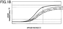
- Fig. 18 shows an example of a linear transmittance value of a light control sheet relative to a voltage applied from one end of an electrode of the light control sheet for each distance from a feeding position.
- the linear transmittance of the light control sheet changes in three levels including halftone (transparent, halftone, and whitish).
- Fig. 18 shows, in a solid line, an example of a change in the linear transmittance relative to the applied voltage in a region of the light control sheet closest to the feeding position.
- dashed lines a, b, and c indicate examples of changes in the linear transmittance relative to the applied voltage in respective regions of the light control sheet.
- the linear transmittance relative to the supply voltage is lower in a region farther from the feeding position in the light control sheet. This is because a wire resistance of a transparent conductive film causes a voltage drop, and thus a lower effective voltage is applied to a light control layer in the region farther from the feeding position.
- a high drive voltage is required to drive a large-area light control sheet so that all regions of the light control sheet are recognized to be transparent, and thus keeping drive power low has been difficult. Accordingly, for example, it has been difficult to drive the large-area light control sheet only with electric power from a solar battery.
- a storage battery storing electric power from the solar battery is used, a storage battery having sufficient capacity needs to be mounted, which may increase the external dimensions or weight of an apparatus in which the light control sheet is mounted.
- the light control sheet When the light control sheet is connected to a fixed power source in order to ensure sufficient drive power source, wires are required for connection, and thus it has been difficult to enable the light control sheet to be movable. For example, it has been difficult to use the light control sheet as movable window glass or partitions.
- the present invention has been made in light of the circumstances described above, and has an object of providing a light control module including a light control sheet which reduces recognition of nonuniformity in transmittance.
- the present invention according to one aspect provides a light control module according to claim 1. Further advantageous developments are defined in the dependent claims.
- the present invention provides a light control module including a light control sheet which reduces recognition of nonuniformity in transmittance.
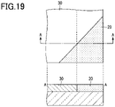
- Fig. 1 is a perspective view schematically illustrating an example of a configuration of a light control module MDL according to an embodiment.
- Fig. 2 is a diagram schematically illustrating an example of a cross section taken along line II-II of the light control module MDL in Fig. 1 .
- a short side (width) direction, a long side (longitudinal) direction, and a thickness (lamination) direction of the light control module MDL are referred to as first direction X, second direction Y, and third direction Z, respectively.
- the light control module MDL of the present embodiment includes a transparent substrate 10, a solar battery 20, a light control sheet 30, and a frame 40.
- the transparent substrate 10, the solar battery 20, and the light control sheet 30 are laminated in the third direction Z.
- the transparent substrate 10 is a transparent insulating substrate made of glass, an acrylic resin, or the like.
- the transparent substrate 10 supports the solar battery 20 and the light control sheet 30 (described later). It is preferable to employ the transparent substrate 10 having a suitable thickness according to the usage such as construction materials, vehicles, automobiles, aircrafts, or ships.
- the light control module is used as a construction material, for example, glass with which the light control module MDL has a thickness of at least 3 mm or more can be used as the transparent substrate 10.
- the solar battery 20 is a photoelectric conversion section which convers light energy from sunlight, illumination light, or the like into power energy, and outputs the power energy.
- the solar battery 20 is a translucent (transparent or semitransparent) photoelectric conversion section laminated on one surface of the transparent substrate 10.
- the solar battery 20 may be formed directly on the transparent substrate 10.
- the solar battery 20 formed on a substrate different from the transparent substrate 10 may be laminated on the transparent substrate 10.
- the light control sheet 30 is arranged on the solar battery 20.
- the light control sheet 30 is a film switchable between the transparent state and the scattering state (opaque state) according to an applied voltage. Furthermore, the light control sheet 30 is switchable between the transparent and halftone states and between the scattering and half tone states according to the applied voltage. In the transparent state, the light control sheet 30 is see-through from both sides thereof. In the opaque state, the light control sheet 30 is not see-through from either side thereof.
- the light control sheet 30 includes a normal-type light control layer which is in the scattering state when no voltage is applied and switches from the scattering state to the transparent state when an applied voltage is increased.
- the light control sheet 30 is not limited to the configuration including the normal-type light control layer and may include a reverse-type light control layer which is in the transparent state when no voltage is applied and switches from the transparent state to the scattering state when an applied voltage is increased.
- the light control sheet 30 includes, as the light control layer, a liquid crystal layer containing a liquid crystal selected from a polymer dispersed liquid crystal (PDLC) and a polymer network liquid crystal (PNLC).
- the light control layer is arranged between transparent electrodes.
- a linear transmittance of the light control sheet 30 is controlled with a voltage applied between the transparent electrodes.
- the light control layer has a thickness of approximately 20 ⁇ m.
- the liquid crystal layer of the light control sheet 30 is not limited to the above configuration.
- the light control sheet 30 may include a light control layer composed of an electrochromic material and capable of controlling a transmittance.
- the light control sheet 30 may include, as the light control layer, a liquid crystal layer composed of a material other than the polymer liquid crystal material.
- the liquid crystal layer as the light control layer can employ various orientation systems such as a TN system, a VA system, an IPS system, an OCB system, and the like.
- the frame 40 surrounds and holds the transparent substrate 10, the solar battery 20, and the light control sheet 30.
- the frame 40 is configured such that a space is formed between the frame 40 and ends of the transparent substrate 10, the solar battery 20, and the light control sheet 30.
- a circuit board (not illustrated), a storage battery, and the like can be housed.
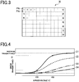
- Fig. 3 is a plan view illustrating an example of a configuration of a light control sheet of a light control module according to an example not forming part of the invention.
- the light control sheet 30 includes a feeding area PIN which applies a voltage to the light control layer.
- the feeding area PIN is provided close to one corner of the light control sheet 30 having a substantially rectangular shape.
- the light control sheet 30 is constituted by virtual regions "1" to "84" for unit area.
- the feeding area PIN is provided in the region "1" of the light control sheet 30. Accordingly, the region closest to the feeding area PIN is the region "1", and the region farthest from the feeding area PIN is the region "84".
- the light control layer of the light control sheet 30 is arranged between the transparent electrodes and is switched between the transparent state and the scattering state according to a voltage applied to the transparent electrodes via the feeding area PIN.
- the resistance of the transparent electrodes causes a voltage drop, and this voltage drop reduces the effective voltage applied to the light control layer. If an effective voltage difference between a position close to the feeding area PIN and a position far therefrom becomes larger, regions of the light control sheet 30 closer to the feeding area PIN are transparent and regions of the light control sheet 30 farther from the feeding area PIN are opaque.
- a difference between a voltage (effective voltage) applied to the light control layer in a unit-area region close to a feeding position and a voltage (effective voltage) applied to the light control layer in a unit-area region far from the feeding position is set to a predetermined value or less.
- Fig. 4 explains an example of a configuration of a light control module according to the present example.
- graph G1 in a solid line shows an example of a relationship between an applied voltage and a linear transmittance of the light control module MDL corresponding to a region of the light control sheet 30 close to the feeding area PIN (e.g., region "1" in Fig. 3 ).
- the relationship between an applied voltage and a transmittance of the light control module MDL has substantially the same characteristics as a relationship between an applied voltage and a transmittance of the light control sheet 30.
- a saturated transmittance (maximum transmittance) when the linear transmittance of the light control module MDL becomes saturated is 67%.
- a minimum transmittance, with which a person recognizes the light control sheet to be opaque, is 0%.
- the tone can be recognized to be different as compared with that in the region close to the feeding area PIN.
- a high voltage is applied to the feeding area PIN in order to obtain a sufficient transmittance in the portion of the light control module MDL corresponding to the region farthest from the feeding area PIN, it has been difficult to keep power consumption of the light control sheet 30 low.
- the inventors of the present application have examined, in the light control module MDL of the present example, an acceptable range for a voltage difference in effective voltage applied to the light control layer between the region close to the feeding area PIN and the region farthest from the feeding area PIN.
- a Munsell value of 90% is equivalent to a transmittance of 78%
- a Munsell value of 50% is equivalent to a transmittance of 19.8%.
- a Munsell value of 100% corresponds to a maximum transmittance of 67% of the light control sheet 30
- a Munsell value of 0% corresponds to a minimum transmittance of 0%, with which a person recognizes the light control sheet to be opaque.
- the entire surface is recognizable as being in the transparent state.
- an applied voltage V50 is approximately 6.7 V.
- graphs G2, G3, and G4 in dashed lines show linear transmittances of respective regions of the light control module MDL relative to a voltage applied to the feeding area PIN.
- the maximum transmittance of the light control module MDL is equivalent to a Munsell value of 100%, and a voltage is applied so that a transmittance equivalent to a Munsell value of 90% is obtained in the portion of the light control module MDL corresponding to the region of the light control sheet 30 closest to the feeding area PIN applying a voltage to the light control layer
- a transmittance in the portion of the light control module MDL corresponding to the region of the light control sheet 30 farthest from the feeding area PIN is not more than a transmittance equivalent to a Munsell value of 50%, the region having a highest transmittance and the region having a lowest transmittance are recognized to have different gradations, and thus the light control sheet 30 is recognized to be nonuniform in transmittance.
- the maximum transmittance of the light control module MDL is equivalent to a Munsell value of 100%, and a voltage is applied so that a transmittance equivalent to a Munsell value of 90% is obtained in the portion of the light control module MDL corresponding to the region of the light control sheet 30 closest to the feeding area PIN applying a voltage to the light control layer
- a transmittance higher than a transmittance equivalent to a Munsell value of 50% is obtained in the portion of the light control module MDL corresponding to the region of the light control sheet 30 farthest from the feeding area PIN, the luminance is recognized to be uniform over the entire surface of the light control sheet 30.
- the inventors of the present application virtually divided the light control sheet 30 into a plurality of regions according to a distance from the feeding area PIN, obtained n graphs G1, G2, G3, ..., and Gn of a linear transmittance relative to an applied voltage in the relative regions in ascending order of a distance from the feeding area PIN, and examined a boundary at which the regions were visually recognized to have different tones.
- the inventors have found that when the luminance at the maximum linear transmittance of the light control sheet 30 is a Munsell value of 100%, and V90 is a voltage with which a transmittance equivalent to a Munsell value of 90% is obtained and V50 is a voltage with which a transmittance equivalent to a Munsell value of 50% is obtained in the region closest to the feeding area PIN, if a transmittance corresponding to V90 in graph Gk (k ⁇ n) is not less than a transmittance corresponding to V50 in graph G1, a voltage drop between the region close to the feeding area PIN and a k-th closest region to the feeding area PIN is small, and thus a transmittance difference (luminance gradient) of the light control sheet 30 is not recognized.
- the inventors of the present application have found that in a region farther from the feeding area PIN than the k-th region is, the transmittance difference (luminance gradient) of the light control sheet 30 is recognized.
- the light control sheet 30 has a width (X direction) of 750 mm and a height (Y direction) of 1700 mm, and in the vicinity of an intersection of a short side and a long side, the light control sheet 30 includes the feeding area PIN of 350 mm extending along the short side.
- the transparent electrode which applies a voltage to the light control layer of the light control sheet 30 is made of ITO.
- the ITO has a sheet resistance R ( ⁇ / ⁇ ) of approximately 100 ( ⁇ ) or more and 300 ( ⁇ ) or less.
- an electrode resistance in the region farthest from the feeding area PIN is approximately in the range of 427 ( ⁇ ) to 1280 ( ⁇ ).
- a difference of approximately 4.3 times in resistance value occurs between the region close to the feeding area PIN and the region farthest from the feeding area PIN, and this difference in resistance value presumably results in a drop in voltage applied from the feeding area PIN at the position far from the feeding area PIN.
- the transmittance of the light control sheet 30 is recognized to be uniform, and the light control module can be driven at a low voltage.
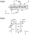
- Fig. 5 is a cross-sectional view schematically illustrating a configuration of a light control sheet of the light control module MDL according to the first example not forming part of the present invention.
- the light control sheet 30 of the present example not forming part of the present invention includes a first substrate 32, a first electrode 34, a first wire W1, a liquid crystal layer LQ, a second wire W2, a second electrode 36, and a second substrate 38.
- the first substrate 32 is a transparent insulating substrate which supports the first electrode 34.
- the first substrate 32 is a film made of polyethylene terephthalate (PET).
- PET polyethylene terephthalate
- the first substrate 32 is a PET film having a thickness of approximately 50 ⁇ m.
- the first substrate 32 preferably has a thickness of 50 ⁇ m or more and 200 ⁇ m or less.
- the first electrode 34 is formed on the first substrate 32.
- the first electrode 34 is a transparent electrode made of a transparent conductive material such as an organic conductive material (e.g., ITO or IZO) or a conductive polymer material (e.g., PEDOT or PEDOT/PSS), and has a thickness of approximately 80 nm or more and 150 nm or less.
- the first electrode 34 is formed over almost an entire surface on a liquid crystal layer LQ side of the first substrate 32.
- the first wire W1 is arranged to form a predetermined pattern (described later) on the first electrode 34.
- the first wire W1 is a wire made of a material whose electrical resistance is lower than that of at least the first electrode 34.
- the first wire W1 is a copper wire.
- a wire made of a material, such as copper, aluminum, or silver, whose electrical resistance is lower than that of the first electrode 34 can be used as the first wire W1.
- a metal thin line has a lower resistance value than an electrode (including the first electrode 34 and the second electrode 36) made of a transparent conductive oxide, the metal thin line is easily visually recognized due to light reflection typical of metal, and a pattern formed by the metal thin line is easily seen. Accordingly, in a light control module including a wire made of metal, it is preferable to make it difficult to visually recognize the wire by reducing surface reflection of the wire.
- first wire W1 and the second wire W2 are made of copper (Cu)
- coating may be formed on a surface of the copper wire by wet processing using various chemicals so that the copper wire takes on a dark color hue such as black, blue, or green.
- the first wire W1 and the second wire W2 instead of forming a monolayer copper wire, it is effective to form, at least above or below a copper layer, a copper oxynitride layer (CuNO) whose reflectance is lower than that of the copper layer.
- a technique is employed in which a first copper oxynitride layer, a copper layer, and a second copper oxynitride layer are sequentially formed on a substrate surface by a sputtering method.
- the copper layer needs to have a thickness of 0.2 ⁇ m or more.
- the thickness of the first and second copper oxynitride layers is preferably 30 nm or more and 50 nm or less and 25% or less of the thickness of the copper layer.
- the first copper oxynitride layer having a thickness of 30 nm or more and 50 nm or less has a sufficient thickness to improve adhesion between the substrate and the copper layer.
- the first copper oxynitride layer having a thickness of 25% or less of the thickness of the copper layer prevents excessive increases in the thickness in the whole wire layer and the amount of copper used, while maintaining adhesion between the substrate and the copper layer.
- the copper oxynitride layer (CuNO) formed by the sputtering method is advantageous for the following reason. That is, although copper nitride (CuN) is chemically unstable, easily reacts with oxygen in air, and greatly changes in optical characteristics (hue) after film forming, the copper oxynitride layer formed by sputtering film forming in which amounts of assist gas of N and O are controlled is easily stabilized in optical characteristics after film forming, and thus such a copper oxynitride layer is advantageous for obtaining a composition having a desired hue.
- a value of Y is preferably 20% or less, and in the Lab color system, L ⁇ is preferably 55 or less and a ⁇ and b ⁇ preferably have negative values.
- the first wire W1 and the second wire W2 are arranged, with a laminate of silver paste and carbon as a primary layer, on a transparent conductive oxide.
- the silver paste of the primary layer improves adhesion between the transparent conductive oxide and the copper wire.
- the carbon of the primary layer flattens asperities on a surface of the silver paste and is interposed between the silver paste and the copper wire.
- a pitch P1 of the first wire W1 in the first direction X is preferably 2.85 mm or less.
- a width P2 of the first wire W1 is preferably sufficiently small enough not to be visually recognized. For example, when the width P2 of the first wire W1 was 20 ⁇ m or less, the first wire W1 was not visually recognized from a position 2 m away.
- the transparent electrode of the light control sheet 30 has a short side of 100 mm, a long side of 1000 mm, and a resistance value of approximately 1200 ⁇ .
- the first wire W1 arranged on the transparent electrode can have a resistance value of 12 ⁇ , which is one hundredth of the resistance value of the transparent electrode.
- a pitch of the copper wires is 2.85 mm.
- the liquid crystal layer LQ is a light control layer which is switchable between the transparent state and the opaque state according to an applied voltage.
- the liquid crystal layer LQ is composed of a polymer dispersed liquid crystal (PDLC) or a polymer network liquid crystal (PNLC).
- the PNLC is composed such that a liquid crystal material is dispersed in a polymer network, and the liquid crystal material in the polymer network has a continuous phase.
- the PDLC is composed such that liquid crystals are dispersed by a polymer, specifically, the liquid crystals are phase-separated in the polymer.
- a photo-curable resin can be used as the polymer layer.
- a solution in which a liquid crystal material is mixed with a photopolymerizable polymer precursor (monomer) is irradiated with ultraviolet light, the monomer is polymerized to form a polymer, and the liquid crystal material is dispersed in a network of the polymer.
- a positive-type (P-type) nematic liquid crystal is used as the liquid crystal material for the liquid crystal layer LQ. That is, when no voltage (no electric field) is applied, long axes (directors) of liquid crystal molecules are randomly orientated, and when a voltage (an electric field) is applied, the directors of the liquid crystal molecules are substantially vertically orientated relative to a base plate surface.
- the liquid crystal layer LQ is a light control layer which is in the opaque state when no voltage is applied and is in the transparent state when a voltage is applied.
- the liquid crystal layer LQ is sealed using a sealant (not illustrated) which bonds the first substrate 32 to the second substrate 38.
- the second substrate 38 is a transparent insulating substrate which supports the second electrode 36.
- the second substrate 38 is a film made of polyethylene terephthalate (PET).
- PET polyethylene terephthalate
- the second substrate 38 is a PET film having a thickness of approximately 50 ⁇ m.
- the second substrate 38 preferably has a thickness of 50 ⁇ m or more and 200 ⁇ m or less.
- the light control module MDL has a thickness of approximately 120 ⁇ m or more and 420 ⁇ m.
- the first substrate 32 and the second substrate 38 are a pair of substrates sandwiching the liquid crystal layer LQ, which is the light control layer.
- the second electrode 36 is formed on the second substrate 38 and is arranged so as to face the first electrode 34.
- the second electrode 36 is a transparent electrode made of a transparent conductive material such as an organic conductive material (e.g., ITO or IZO) or a conductive polymer material (e.g., PEDOT or PEDOT/PSS), and has a thickness of approximately 80 nm or more and 150 nm or less.
- the second electrode 36 is formed over almost an entire surface on a liquid crystal layer LQ side of the second substrate 38.
- the second wire W2 is arranged to form a predetermined pattern (described later) on the second electrode 36.
- the second wire W2 is a wire made of a material whose electrical resistance is lower than that of at least the second electrode 36.
- the second wire W2 is a copper wire.
- a wire made of a material, such as copper, aluminum, or silver, whose electrical resistance is lower than that of the second electrode 36 can be used as the second wire W2.
- a pitch P3 of the second wire W2 in the first direction X is preferably 2.85 mm or less.
- a width P4 of the second wire W2 is preferably sufficiently small enough not to be visually recognized. For example, when the width P4 of the second wire W2 was 20 ⁇ m or less, the second wire W2 was not visually recognized from a position 2 m away.
- the first wire W1 and the second wire W2 include wire sections (first wire sections and third wire section described later) extending in a depth direction (second direction Y) in Fig. 5 and are arranged adjacent to each other with a predetermined pitch in a width direction (first direction X) in Fig. 5 .
- the first wire W1 is arranged so as to face a position on the second electrode 36 at which the second wire W2 is not arranged
- the second wire W2 is arranged so as to face a position on the first electrode 34 at which the first wire W1 is not arranged.
- first wire W1 and the second wire W2 may be arranged so as to face each other, by arranging the first wire W1 so as to face a position at which the second wire W2 is not arranged, it is possible to avoid variations in transmittance when the first wire W1 and the second wire W2 are formed at deviated positions and avoid deterioration in quality of the light control sheet due to moire or the like.
- Fig. 6 explains an example configuration of the first wire W1 and the second wire W2 of the light control sheet 30 of the light control module MDL of the first example not forming part of the present invention.
- the first wire W1 and the second wire W2 form the same pattern
- Fig. 6 illustrates the pattern that the first wire W1 and the second wire W2 form in common.
- the first wire W1 has a plurality of first wire sections WY extending in the second direction Y and a plurality of second wire sections WX extending in the first direction X between the first wire sections WY.
- the second wire W2 has a plurality of third wire sections WY extending in the second direction Y and a plurality of fourth wire sections WX extending in the first direction X between the third wire sections WY.
- the second wire sections WX adjacent to each other in the first direction X are arranged at different positions in the second direction Y.
- a pitch P5 between the second wire sections WX is approximately 1100 ⁇ m.
- the first wire sections WY are electrically connected to each other via the second wire sections WX.
- the first wire W1 and the second wire W2 are a conductive film having a mesh shape.
- the cut piece includes the metal wire (the first wire W1 and the second wire W2), and thus a lower resistance effect is maintained.
- the wire widths P2 and P4 are preferably 20 ⁇ m or less, and the pitches P1 and P3 between the first wire sections WY are preferably 2.85 mm or less.
- the following discussion will examine, for example, a case where a plurality of copper wires extending in the long side direction are formed with a pitch of 0.3 mm on an ITO electrode having a short side of 10 mm and a long side of 1000 mm.
- the ITO has a sheet resistance of approximately 100 ⁇ .
- Copper has a resistivity of 1.68 ⁇ 10 -8 Qm.
- approximately 33 (10 mm ⁇ 0.3 mm ⁇ 33) copper wires are arranged on the ITO electrode.
- Each of the copper wires has a resistance value R Cu1m as below.
- the resistance value of the copper wire is sufficiently smaller than the resistance value of the ITO electrode. Accordingly, the arrangement of the copper wires on the ITO electrode can reduce a voltage gradient which occurs according to a distance from a feeding position when a voltage is applied to the ITO electrode and the copper wires.
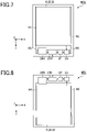
- Fig. 7 is a block diagram schematically illustrating an example of a drive circuit of the light control module MDL according to the first example not forming part of the present invention.
- the light control module MDL of the present example not forming part of the present invention includes a controller CTR, a drive circuit DRV, a storage battery BT, and a charge/discharge circuit CH.
- the controller CTR, the drive circuit DRV, the storage battery BT, and the charge/discharge circuit CH are housed in a space inside the frame 40 of the light control module MDL.
- the controller CTR is an arithmetic circuit including a processor (not illustrated), such as a CPU or MPU, and a memory (not illustrated).
- the controller CTR can communicate with external devices, receive detection values from various sensors or command values from interfaces such as user-operable remote controls, and control the drive circuit DRV based on the received values.
- the charge/discharge circuit CH charges the storage battery with an electric current outputted from the solar battery 20 and supplies a DC voltage from the storage battery to the drive circuit.
- the charge/discharge circuit CH controls a charging current of the storage battery BT according to a voltage or the like of the storage battery BT.
- the charge/discharge circuit CH discharges the storage battery BT and supplies a DC voltage to the drive circuit DRV.
- the charge/discharge circuit CH may be configured such that when the storage battery BT is fully charged, an output voltage of the solar battery 20 is outputted to the drive circuit DRV.
- the drive circuit DRV includes a boost circuit, a frequency oscillator, and a switching circuit.
- the boost circuit boosts a voltage supplied from the storage battery BT according to a drive voltage of the light control sheet 30.
- the drive voltage of the light control sheet 30 is set by commands from the control circuit CTR.
- the frequency oscillator generates a frequency of the drive voltage of the light control sheet 30.
- the frequency of the drive voltage of the light control sheet 30 is set by commands from the control circuit CTR.
- the operation of the switching circuit is controlled by the control circuit CTR so that the light control sheet 30 is switched between a drive state and a stop state.
- a feeding wire W3 is connected between the drive circuit DRV and each of the first wire W1 and the second wire W2.
- the feeding wire W3 is made of a material whose electrical resistance is lower than that of the first electrode 34 and the second electrode 36.
- the feeding wire W3 is a metal wire made of copper, silver, or the like.
- the feeding wire W3 is bent so that no water droplets enter the circuits through the feeding wire W3.
- the feeding wire W3 extends from the first wire W1 and the second wire W2 toward a lower side of the frame 40 (an outer edge side of the frame 40), is bent in a substantially U-shape, which is convex downward, and is then electrically connected to the drive circuit DRV.
- the substantially U-shaped bent portion has a width of 10 mm or more in the Y direction of the feeding wire W3 and a width of 5 mm or more in the X direction of the feeding wire W3.
- the drive circuit DRV, the control circuit CTR, the storage battery BT, and the charge/discharge circuit CH are preferably installed with a spacing of 5 mm or more from a base of the frame 40.
- the drive circuit DRV and the like do not immediately become wet, and breakdown of the light control module MDL can be avoided.
- Fig. 8 is a block diagram schematically illustrating another example of the drive circuit of the light control module according to the first example not forming part of the present invention.
- the drive circuit DRV, the control circuit CTR, the storage battery BT, and the charge/storage circuit CH are arranged, on an upper side of the solar battery 20 and the light control sheet 30, inside the frame 40.
- the drive circuit DRV, the control circuit CTR, the storage battery BT, and the charge/storage circuit CH are installed at the upper portion of the frame, it is possible to prevent water caused by condensation or the like from entering through the feeding wire W3. Accordingly, the feeding wire W3 does not need to be bent, and thus the feeding wire W3 can have a shorter wire length.
- a voltage applied to the light control layer (liquid crystal layer LQ) in the region farthest from the feeding position was approximately equal to a voltage applied to the light control layer in the region close to the feeding position.
- a difference in the voltage applied to the light control layer (liquid crystal layer LQ) between the region close to the feeding position and the region farthest from the feeding position was 4.6 V or less, and the luminance was recognized to be uniform over the entire surface of the light control sheet 30.
- the transmittance of the light control sheet 30 is recognized to be uniform, and the drive voltage of the light control sheet 30 can be kept low, and thus lower power consumption of the light control module MDL is achieved. That is, the present example not forming part of the present invention makes it possible to provide a light control module MDL which can be driven at a low voltage.
- the light control module MDL of the present example not forming part of the present invention integrally includes the solar battery 20 and a storage battery unit BT so that the light control module MDL can be driven with electric power supplied from these components. Accordingly, the light control module MDL of the present example not forming part of the present invention can be installed at a movable portion or a portion in which wiring is difficult.
- the light control module MDL of the present example not forming part of the present invention does not need to be fixed in real estate such as an architectural structure, and thus the light control module MDL is easily replaced when the operating life expires.
- the light control module MDL of the present example was a light control module used for a common home-use aluminum sash sliding door, and the external dimensions of the frame 40 were approximately 810 mm in width (short side) and approximately 900 mm in height (long side) (half of 1620 mm in width and 1800 mm in height). In this case, dimensions of the solar battery 20 and the light control sheet 30 were approximately 750 mm in width and approximately 1700 mm in height.
- the first electrode 34 and the second electrode 36 of the light control sheet 30 were made of ITO having a predetermined thickness.
- the first wire W1 and the second wire W2 had a thickness of 2 ⁇ m, the wire widths P2 and P4 were 20 ⁇ m, the wire pitches P1 and P3 were 300 ⁇ m, and the wire pitch P5 was 1100 ⁇ m.
- the liquid crystal layer LQ was composed of PNLC.
- a voltage applied to the light control layer (liquid crystal layer LQ) in the region farthest from the feeding position was approximately equal to a voltage applied to the light control layer in the region close to the feeding position.
- a difference in the voltage applied to the light control layer (liquid crystal layer LQ) between the region close to the feeding position and the region farthest from the feeding position was 4.6 V or less, and the luminance was recognized to be uniform over the entire surface of the light control sheet 30.
- the drive voltage of the light control sheet 30 can be kept low, and thus an effect similar to that of the light control module MDL of the first example not forming part of the present invention is yielded.
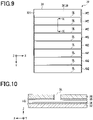
- Fig. 9 is a plan view schematically illustrating an example of a configuration of the light control sheet of the light control module MDL according to the second example not forming part of the present invention.
- Fig. 10 is a diagram schematically illustrating an example of a cross section taken along line IX-IX of the light control sheet 30 in Fig. 9 .
- the light control module MDL of the present example not forming part of the present invention differs from the first example not forming part of the present invention in the configuration of the first wire W1, the second wire W2, the second electrode 36, and the second substrate 38 of the light control sheet 30.
- the first wire W1 of the light control sheet 30 is arranged along a long side of the first electrode 34.
- Fig. 9 does not illustrate the first electrode 34
- the first electrode 34 has a substantially rectangular shape having a long side extending in the Y direction and a short side extending in the X direction and is arranged over almost an entire part of one surface of the first substrate 32.
- the second electrode 36 and the second substrate 38 of the light control sheet 30 are separated into a plurality of strips by slits SL extending in the X direction.
- the light control sheet 30 of the present example not forming part of the present invention includes the plurality of second wires W2 which are electrically connected to the respective strips of the second electrode 36.
- the second wires W2 are each arranged along a long side of the light control sheet 30 facing the long side along which the first wire W1 is arranged. According to the present example not forming part of the present invention, therefore, a sum of a distance to the first wire W1 and a distance to the second wire W2 is the same at any position in the light control sheet 30.
- a supply voltage is applied to the first electrode 34 from one side in the X direction, and a supply voltage is applied to the second electrode 36 from the other side in the X direction.
- an effective voltage applied to the liquid crystal layer LQ which is the light control layer, is approximately the same at any position in the X direction.
- a voltage of the first wire W1 is approximately the same in the Y direction as that of the second wire W2. Accordingly, when the light control sheet 30 is driven, an effective voltage gradient is approximately zero in the plane direction of the light control sheet 30.
- the light control module MDL of the present example not forming part of the present invention is similar to the first example not forming part of the present invention except for the above configuration of the light control sheet 30.
- a voltage applied to the light control layer (liquid crystal layer LQ) in the region farthest from the feeding position was approximately equal to a voltage applied to the light control layer in the region close to the feeding position.
- a difference in the voltage applied to the light control layer (liquid crystal layer LQ) between the region close to the feeding position and the region farthest from the feeding position was 4.6 V or less, and the luminance was recognized to be uniform over the entire surface of the light control sheet 30.
- the light control module MDL of the present example not forming part of the present invention yields an effect similar to that of the first example not forming part of the present invention and makes it possible to provide a light control module MDL which can be driven at a low voltage.
- Figs. 11A and 11B are each a diagram illustrating an electrode structure of a light control sheet of a light control module.
- the first wire W1 and the second wire W2 are arranged along the respective facing long sides of the light control sheet 30.
- the first wire W1 and the second wire W2 are not limited to the configuration illustrated in Figs. 9 and 10 .
- the first wire W1 and the second wire W2 only need to be arranged so that the sum of the distance to the first wire W1 and the distance to the second wire W2 is the same at any position in the light control sheet 30.
- the second wire W2 may be arranged in a circular shape around the first wire W1.
- the sum of the distance to the first wire W1 and the distance to the second wire W2, which is a radius R, is the same at any position in the circle surrounded by the second wire W2.
- the first wire W1 and the second wire W2 may be arranged in substantially W-shapes facing each other. Also in this case, at any position in the light control sheet 30, the sum of the distance to the first wire W1 and the distance to the second wire W2 is the same as a space d between the first wire W1 and the second wire W2, and thus an effect similar to that of the second example not forming part of the present invention is yielded.
- Fig. 12 is a diagram schematically illustrating an example of a cross section of the light control module MDL according to the third example not forming part of the present invention.
- the light control module MDL of the present example not forming part of the present invention differs from the first example not forming part of the present invention in the configuration of the solar battery 20.
- the solar battery 20 is arranged on one surface substantially orthogonal to the lamination direction Z of the frame 40. Specifically, the solar battery 20 is arranged in a picture frame shape surrounding the transparent substrate 10 and the light control sheet 30. According to the present example not forming part of the present invention, the solar battery 20 is arranged on a surface of the frame 40 on a transparent substrate 10 side in the lamination direction Z, and the solar battery 20 converts light energy from sunlight or illumination light incident from the transparent substrate 10 side into electric energy, and outputs the electric energy.
- the frame 40 holds a periphery of the transparent substrate 10 and the light control sheet 30.
- the solar battery 20 is arranged on one surface substantially orthogonal to the lamination direction Z of the frame 40.
- another solar battery 20 may be arranged on the other surface substantially orthogonal to the lamination direction Z of the frame 40.
- an area in which the solar battery 20 is arranged is ensured on both surfaces of the frame 40, leading to decrease in the width of the frame 40.
- the solar battery 20 is the translucent (transparent or semitransparent) photoelectric conversion section. According to the present example not forming part of the present invention, however, since the solar battery 20 is arranged on the frame 40, the solar battery 20 is not limited to the translucent photoelectric conversion section, and thus a solar battery having high energy conversion efficiency can be selected as the solar battery 20 of the present example not forming part of the present invention.
- the light control module MDL of the present example not forming part of the present invention is similar to the first example not forming part of the present invention except for the above configuration. That is, the light control module MDL of the present example not forming part of the present invention yields an effect similar to that of the first example not forming part of the present invention.
- the solar battery 20 does not need to be arranged over an entire surface of the frame 40 surrounding the transparent substrate 10 and the light control sheet 30. Depending on sunshine conditions and the like in a place where the light control module MDL is installed, the solar battery 20 may be arranged on a part of the surface substantially orthogonal to the lamination direction Z of the frame 40. Also in such a case, when a sufficient area is ensured in consideration of energy generated by the solar battery 20, an effect similar to that of the first example not forming part of the present invention is yielded. (Example 2)
- the light control module MDL of the present example included the light control sheet 30 having a short side of 1000 mm and a long side of 1200 mm.
- the storage battery unit BT includes three lithium ion batteries in which a voltage is 4.1 V and an electric current is 1.8 Ah, and the light control sheet 30 is driven with electric power supplied from the storage battery unit BT.
- the present example employed, as the solar battery 20, a solar battery whose area was 180 mm ⁇ 222 mm and whose main component was a single crystal silicon semiconductor.
- the solar battery 20 a solar battery whose area was 180 mm ⁇ 222 mm and whose main component was a single crystal silicon semiconductor.
- an output voltage was 9 V
- an output current was 440 mA
- output power was approximately 4W.
- the light control module MDL of the present example As described above, according to the light control module MDL of the present example, an effect similar to that of the first example not forming part of the present invention was yielded, and by keeping the drive voltage of the light control module MDL low, the light control module MDL was able to be continuously driven for more than 7 hours with the electric power stored in the storage battery of the storage battery unit BT.
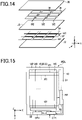
- Fig. 13 is a cross-sectional view schematically illustrating a configuration of the light control sheet 30 of the light control module MDL according to the first embodiment.
- Fig. 14 is an exploded perspective view schematically illustrating the configuration of the light control sheet 30 of the light control module MDL according to the first embodiment.
- the light control module MDL of the present embodiment differs from the first example not forming part of the present invention in the configuration of the light control sheet 30.
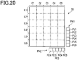
- the light control sheet 30 of the present embodiment includes the first substrate 32, the plurality of first electrodes 34, the plurality of first wires W1, the liquid crystal layer LQ, the plurality of second wires W2, the plurality of second electrodes 36, and the second substrate 38.
- the first electrodes 34 are arranged in a matrix form in a plane direction substantially parallel to the first direction X and the second direction Y (on a virtual plane substantially orthogonal to the lamination direction Z) on a surface on the liquid crystal layer LQ side of the first substrate 32.
- the first electrodes 34 are each made of a transparent conductive material, such as ITO, IZO, or an organic conductive film, and have a thickness of approximately 80 nm or more and 150 nm or less.
- the first wires W1 each extend in the first direction X between rows of the first electrodes 34 arranged adjacent to each other in the first direction X.
- the first wires W1 are insulated from each other.
- the first wires W1 are each electrically connected to the first electrodes 34 arranged on one side in the second direction Y. Specifically, when a drive voltage is applied to one of the first wires W1, a drive voltage is applied to the first electrodes 34 in the row adjacent to the one of the first wires W1.
- the second electrodes 36 are arranged in a matrix form so as to face the first electrodes 34 in a plane direction substantially parallel to the first direction X and the second direction Y (on a plane substantially parallel to the virtual plane on which the first electrodes 34 are arranged) on a surface on the liquid crystal layer LQ side of the second substrate 38.
- the second electrodes 36 are arranged at positions facing the respective first electrodes 34.
- the second electrodes 36 are each made of a transparent conductive material such as ITO or IZO and have, for example, a thickness of approximately 80 nm or more and 150 nm or less.
- the second wires W2 each extend in the second direction Y between columns of the second electrodes 36 arranged adjacent to each other in the second direction Y.
- the second wires W2 are insulated from each other.
- the second wires W2 are each electrically connected to the second electrodes 36 arranged on one side in the first direction X. Specifically, when a drive voltage is applied to one of the second wires W2, a drive voltage is applied to the second electrodes 36 in the column adjacent to the one of the second wires W2.
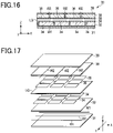
- Fig. 15 is a block diagram schematically illustrating an example of a drive circuit of the light control module according to the first embodiment.
- the light control module MDL of the present embodiment includes the controller CTR, the drive circuit DRV, the storage battery unit BT, and selectors S1 and S2.
- the controller CTR, the drive circuit DRV, the storage battery unit BT, and the selectors S1 and S2 are housed in a space inside the frame 40 of the light control module MDL.
- the controller CTR is an arithmetic circuit including a processor (not illustrated), such as a CPU or MPU, and a memory (not illustrated).
- the controller CTR can communicate with external devices, receive detection values or commands from various sensors, commands from interfaces such as user-operable remote controls, or the like, and control the drive circuit DRV and the selectors S1 and S2 based on the received commands or the like.
- the controller CTR controls the selectors S1 and S2 so that a part of the light control sheet 30 is in the transparent state or the opaque state.
- the storage battery unit BT includes the storage battery BT of the first example not forming part of the present invention and the charge/discharge circuit CH.
- the charge/discharge circuit CH controls a charging current of the storage battery BT according to a voltage or the like of the storage battery BT.
- the charge/discharge circuit CH discharges the storage battery BT and supplies a DC voltage to the drive circuit DRV.
- the charge/discharge circuit CH may be configured such that when the storage battery BT is fully charged, an output voltage of the solar battery 20 is outputted to the drive circuit DRV.
- the drive circuit DRV includes a boost circuit and a frequency oscillator.
- the boost circuit boosts a voltage supplied from the storage battery according to a drive voltage of the light control sheet 30.
- the drive voltage of the light control sheet 30 is set by commands from the control circuit CTR.
- the frequency oscillator generates a frequency of the drive voltage of the light control sheet 30.
- the frequency of the drive voltage of the light control sheet 30 is set by commands from the control circuit CTR.
- the operation of the selector S1 is controlled by the control circuit CTR so that one or more of the first wires W1 is selected and a drive voltage supplied from the drive circuit DRV is supplied to the selected one or more of the first wires W1.
- the operation of the selector S2 is controlled by the control circuit CTR so that one or more of the second wires W2 is selected and a drive voltage supplied from the drive circuit DRV is supplied to the selected one or more of the second wires W2.
- control circuit CTR, the drive circuit DRV, and the selectors S1 and S2 are mounted on a double-sided base plate, and the selector S1 is mounted on a surface different from a surface on which the control circuit CTR, the drive circuit DRV, and the selector S2 are mounted.
- the drive voltage of the light control sheet 30 can be kept low by separating the first electrodes 34 and the second electrodes 36 in the form of islands and driving the first electrodes 34 and the second electrodes 36 through the first wires W1 and the second wires W2, thus achieving lower power consumption of the light control module MDL.
- the light control module MDL of the present embodiment is applicable when upsizing the light control module MDL.
- the light control module MDL of the present embodiment can be configured by combining two or more of the light control sheets 30 of the light control modules MDL of the first to third examples and first embodiment. Also in such a case, power consumption of the light control module MDL can be kept low.
- the maximum transmittance of the light control module MDL was equivalent to a Munsell value of 100%, and a voltage was applied so that a transmittance equivalent to a Munsell value of 90% was obtained in the portion of the light control module MDL corresponding to the region of the light control sheet 30 closest to the feeding area applying a voltage to the light control layer
- a transmittance higher than a transmittance equivalent to a Munsell value of 50% was obtained in the portion of the light control module MDL corresponding to the region of the light control sheet 30 farthest from the feeding area, and the luminance was recognized to be uniform over the entire surface of the light control sheet 30.
- the feeding area corresponds to the feeding position of each of the transparent electrodes.
- the present embodiment makes it possible to provide a light control module MDL which can be driven at a low voltage.
- the light control module MDL of the present embodiment can be driven with electric power supplied from the solar battery 20 and the storage battery unit BT, the light control module MDL of the present embodiment can be installed at a movable portion or a portion in which wiring is difficult.
- the light control module MDL of the present embodiment does not need to be fixed in real estate such as an architectural structure, and thus the light control module MDL is easily replaced when the operating life expires.
- a drive voltage can be selectively applied to the first electrodes 34 and the second electrodes 36. Specifically, a drive voltage can be applied only to the first electrode 34 and the second electrode 36 which are arranged at a position at which the selected first wire W1 intersects with the selected second wire W2, thus enabling a part of the light control sheet 30 to be switched between the transparent state and the opaque state.
- Fig. 16 is a cross-sectional view schematically illustrating a configuration of the light control sheet 30 of the light control module MDL according to the second embodiment.
- Fig. 17 is an exploded perspective view schematically illustrating the configuration of the light control sheet 30 of the light control module MDL according to the second embodiment.
- the light control module MDL of the present embodiment differs from the first embodiment described above in the configuration of the light control sheet 30.
- the light control sheet 30 of the present embodiment includes a first protection layer 31, the first substrate 32, the plurality of first electrodes 34, the plurality of first wires W1, the liquid crystal layer LQ, the plurality of second wires W2, the plurality of second electrodes 36, the second substrate 38, and a second protection layer 39.
- the first electrodes 34 are arranged in a matrix form in the first direction X and the second direction Y on a surface on the liquid crystal layer LQ side of the first substrate 32.
- the first electrodes 34 are each made of a transparent conductive material such as ITO, IZO, or an organic conductive film and have, for example, a thickness of approximately 80 nm or more and 150 nm or less.
- the first wires W1 each extend in the first direction X on an outer surface of the first substrate 32.
- the first wires W1 are each arranged so as to face a row of the first electrodes 34 arranged adjacent to each other in the first direction X with the first substrate 32 therebetween.
- the first wires W1 are each electrically connected to the facing first electrodes 34 via through holes formed on the first substrate 32.
- the first wires W1 are insulated from each other. Specifically, when a drive voltage is applied to one of the first wires W1, a drive voltage is applied to the first electrodes 34 electrically connected to the one of the first wires W1.
- the first protection layer 31 is arranged on the first wires W1.
- the first protection layer 31 is a transparent insulation layer and is, for example, made of PET.
- the second electrodes 36 are arranged in a matrix form in the first direction X and the second direction Y on a surface on the liquid crystal layer LQ side of the second substrate 38.
- the second electrodes 36 are arranged at positions facing the respective first electrodes 34.
- the second electrodes 36 are each made of a transparent conductive material such as ITO or IZO and have, for example, a thickness of approximately 80 nm or more and 150 nm or less.
- the second wires W2 each extend in the second direction Y on an outer surface of the second substrate 38.
- the second wires W2 are each arranged so as to face a column of the second electrodes 36 arranged adjacent to each other in the second direction Y with the second substrate 38 therebetween.
- the second wires W2 are each electrically connected to the facing second electrodes 36 via through holes formed on the second substrate 38.
- the second wires W2 are insulated from each other. Specifically, when a drive voltage is applied to one of the second wires W2, a drive voltage is applied to the second electrodes 36 electrically connected to the one of the second wires W2.
- the second protection layer 39 is arranged on the second wires W2.
- the second protection layer 39 is a transparent insulation layer and is, for example, made of PET.
- the light control module MDL of the present embodiment is similar to the first embodiment except for the above configuration of the light control sheet 30.
- the drive voltage of the light control sheet 30 can be kept low by separating the first electrodes 34 and the second electrodes 36 in the form of islands and driving the first electrodes 34 and the second electrodes 36 through the first wires W1 and the second wires W2, thus achieving lower power consumption of the light control module MDL.
- the light control module MDL of the present embodiment is applicable when upsizing the light control module MDL.
- the light control module MDL of the present embodiment can be configured by combining two or more of the light control sheets 30 of the light control modules MDL of the first to third examples and first embodiment. Also in such a case, power consumption of the light control module MDL can be kept low.
- the maximum transmittance of the light control module MDL was equivalent to a Munsell value of 100%, and a voltage was applied so that a transmittance equivalent to a Munsell value of 90% was obtained in the portion of the light control module MDL corresponding to the region of the light control sheet 30 closest to the feeding area applying a voltage to the light control layer
- a transmittance higher than a transmittance equivalent to a Munsell value of 50% was obtained in the portion of the light control module MDL corresponding to the region of the light control sheet 30 farthest from the feeding area, and the luminance was recognized to be uniform over the entire surface of the light control sheet 30.
- the feeding area corresponds to the feeding position of each of the transparent electrodes.
- the present embodiment makes it possible to provide a light control module MDL which can be driven at a low voltage.
- the light control module MDL of the present embodiment can be driven with electric power supplied from the solar battery 20 and the storage battery unit BT, the light control module MDL of the present embodiment can be installed at a movable portion or a portion in which wiring is difficult.
- the light control module MDL of the present embodiment does not need to be fixed in real estate such as an architectural structure, and thus the light control module MDL is easily replaced when the operating life expires.
- a drive voltage can be selectively applied to the first electrodes 34 and the second electrodes 36. Specifically, a drive voltage can be applied only to the first electrode 34 and the second electrode 36 which are arranged at a position at which the selected first wire W1 intersects with the selected second wire W2, thus enabling a part of the light control sheet 30 to be switched between the transparent state and the opaque state.
- Fig. 19 is a diagram illustrating an example of a configuration of a light control sheet and a solar battery of a light control module according to an embodiment.
- the light control sheet 30 and the solar battery 20 may include a common substrate made of glass, an acrylic resin, a PET film, or the like.
- the light control sheet 30 may be a light control layer formed in a partial region on the common substrate
- the solar battery 20 may be a photoelectric conversion layer formed so as to be arranged adjacent to the light control layer of the light control sheet 30 in another region on the common substrate.
- the common substrate has a substantially rectangular shape, and the solar battery 20 is arranged at a corner portion of the common substrate.
- the light control sheet 30 may be a light control layer formed on one surface of the common substrate, and the solar battery 20 may be a photoelectric conversion layer formed on the other surface of the common substrate.
- a transparent plate made of glass, an acrylic resin, or the like, or a transparent film such as a PET film can be used as the common substrate.
- the solar battery 20 is preferably arranged in a portion irradiated with sunlight.
- the positions of the solar battery 20 and the light control sheet 30 and the area in which the solar battery 20 is arranged are preferably adjusted as appropriate according to the environment where the light control module is installed.
- a transmittance is uncontrollable in a region in which the solar battery 20 is arranged, and thus the positions of the solar battery 20 and the light control sheet 30 and the area in which the solar battery 20 is arranged are preferably adjusted as appropriate according to the usage of the light control module.
- Fig. 20 is a diagram illustrating an example of an operation section of a light control module according to an embodiment.
- one of the first electrode 34 and the second electrode 36 of the light control sheet 30 may be divided into a plurality of regions L1 to L6 and C1 to C5 so that the regions L1 to L6 and C1 to C5 can be independently driven.
- the operation section which operates a drive state of the regions L1 to L6 and C1 to C5 may be mounted in the frame 40 of the light control module MDL or outside the frame 40.
- the operation section may be configured to include touch panels PN1 and PN2 corresponding to the regions of the light control sheet 30 and configured such that a drive state of each of the regions L1 to L6 and C1 to C5 of the light control sheet 30 is changeable by touching one of touch panels PL1 to PL6 and PC1 to PC5 corresponding to a region in which a transmittance (or luminance) is desired to be switched among the regions L1 to L6 and C1 to C5 of the light control sheet 30.
- a user can conduct an operation so that a transmittance (or luminance) in the region L1 of the light control sheet 30 is switched, and by touching the touch panel PC3, the user can conduct an operation so that a transmittance (or luminance) in the region C3 of the light control sheet 30 is switched.
- the touch panel PN1 successively from PL1 toward PL6 in a line, the user can conduct an operation so that a transmittance (or luminance) is continuously switched in the regions from the region L1 toward the region L6 of the light control sheet 30.
Landscapes
- Physics & Mathematics (AREA)
- Nonlinear Science (AREA)
- Chemical & Material Sciences (AREA)
- Crystallography & Structural Chemistry (AREA)
- General Physics & Mathematics (AREA)
- Optics & Photonics (AREA)
- Mathematical Physics (AREA)
- Engineering & Computer Science (AREA)
- Structural Engineering (AREA)
- Architecture (AREA)
- Civil Engineering (AREA)
- Dispersion Chemistry (AREA)
- Geometry (AREA)
- Liquid Crystal (AREA)
- Planar Illumination Modules (AREA)
- Photovoltaic Devices (AREA)
Claims (9)
- Lichtsteuerungsmodul (MDL), mit:einer Lichtsteuerungsfolie (30) miteiner Lichtsteuerungsschicht (LQ), die in Abhängigkeit von einer angelegten Spannung zwischen einem transparenten Zustand und einem undurchsichtigen Zustand umschaltbar ist,mindestens einer ersten Elektrode (34), die aus einem transparenten leitfähigen Material besteht,mindestens einer zweiten Elektrode (36), die so angeordnet ist, dass sie der mindestens einen ersten Elektrode (34) mit der Lichtsteuerungsschicht (LQ) dazwischen zugewandt ist, und die aus einem transparenten leitfähigen Material besteht,einer Vielzahl von ersten Drähten (W1) undeiner Vielzahl von zweiten Drähten (W2); undeiner Ansteuerungsschaltung (DRV), die über einen Spannungsversorgungsbereich (PIN) der Lichtsteuerungsfolie (30) eine Spannung an die mindestens eine erste Elektrode (34) und die mindestens eine zweite Elektrode (36) der Lichtsteuerungsfolie (30) anlegt;wobei die Vielzahl von ersten Drähte (W1) aus einem Material hergestellt ist, dessen elektrischer Widerstand geringer als der der Vielzahl von ersten Elektroden ist, und die Vielzahl von zweiten Drähte (W2) aus einem Material hergestellt ist, dessen elektrischer Widerstand geringer als der der Vielzahl der zweiten Elektroden ist, unddadurch gekennzeichnet, dassdie mindestens eine erste Elektrode (34) eine Vielzahl von ersten Elektroden (34) umfasst;die mindestens eine zweite Elektrode (36) eine Vielzahl von zweiten Elektroden (36) umfasst;die ersten Elektroden (34) in einer Matrixform auf einer virtuellen Ebene angeordnet sind, die im Wesentlichen orthogonal zu einer Richtung ist, in der die Lichtsteuerungsfolie (30), die ersten Elektroden (34) und die zweiten Elektroden (36) laminiert sind;die zweiten Elektroden (36) in einer Matrixform auf einer Ebene angeordnet sind, die im Wesentlichen parallel zu der virtuellen Ebene ist, so dass sie den ersten Elektroden (34) zugewandt ist;die ersten Drähte (W1) elektrisch mit den ersten Elektroden (34) verbunden sind, die in einer ersten Richtung nebeneinander angeordnet sind; unddie zweiten Drähte (W2) elektrisch mit den zweiten Elektroden (36) verbunden sind, die in einer zweiten Richtung nebeneinander angeordnet sind, die sich von der ersten Richtung unterscheidet, wobei die Vielzahl von ersten Elektroden, die Vielzahl von zweiten Elektroden, die ersten Drähte und die zweiten Drähte so angeordnet sind, dass,wenn ein maximaler Transmissionsgrad der Lichtsteuerungsfolie (30) einem Munsell-Wert von 100 % entspricht, wobei ein Transmissionsgrad, der aus einer Multiplikation des maximalen Transmissionsgrads mit 0,787 berechnet wird, einem Munsell-Wert von 90 % entspricht und ein Transmissionsgrad, der aus einer Multiplikation des maximalen Transmissionsgrads mit 0,198 berechnet wird, einem Munsell-Wert von 50 % entspricht,und die Ansteuerungsschaltung (DRV) eine Spannung derart anlegt, dass in einem Gebiet der Lichtsteuerungsfolie (30), das dem Spannungsversorgungsbereich (PIN) am nächsten liegt, ein Transmissionsgrad erreicht wird, der dem Munsell-Wert von 90 % entspricht,dann wird in einem Gebiet der Lichtsteuerungsfolie (30), das am weitesten von dem Spannungsversorgungsbereich entfernt ist, ein Transmissionsgrad erreicht, der höher als ein Transmissionsgrad ist, der dem Munsell-Wert von 50 % entspricht.
- Lichtsteuerungsmodul (MDL) nach Anspruch 1, wobeidie ersten Drähte (W1) sich jeweils in der ersten Richtung zwischen Reihen der ersten Elektroden (34) erstrecken, die in der ersten Richtung nebeneinander angeordnet sind; unddie zweiten Drähte (W2) sich jeweils in der zweiten Richtung zwischen Spalten der zweiten Elektroden (36) erstrecken, die in der zweiten Richtung nebeneinander angeordnet sind.
- Lichtsteuerungsmodul (MDL) nach Anspruch 1, ferner mit:einem ersten Substrat (32), das die ersten Elektroden (34) trägt; undeinem zweiten Substrat (38), das die zweiten Elektroden (36) trägt, wobeidie ersten Drähte (W1) jeweils so angeordnet sind, dass sie einer Reihe der ersten Elektroden (34) zugewandt sind, die in der ersten Richtung nebeneinander angeordnet sind, wobei sich das erste Substrat (32) dazwischen befindet, und mit den zugewandten ersten Elektroden (34) über ein auf dem ersten Substrat (32) ausgebildetes Durchloch elektrisch verbunden sind; unddie zweiten Drähte (W2) jeweils so angeordnet sind, dass sie einer Spalte der zweiten Elektroden (36) zugewandt sind, die in der zweiten Richtung nebeneinander angeordnet sind, wobei sich das zweite Substrat (38) dazwischen befindet, und sie mit den zugewandten zweiten Elektroden (36) über ein auf dem zweiten Substrat (38) ausgebildetes Durchloch elektrisch verbunden sind.
- Lichtsteuerungsmodul (MDL) nach einem der Ansprüche 1 bis 3, wobei die ersten Drähte (W1) und die zweiten Drähte (W2) eine Breite (P2, P4) von 20 µm oder weniger aufweisen.
- Lichtsteuerungsmodul (MDL) nach einem der Ansprüche 1 bis 4, wobei die Lichtsteuerungsschicht (LQ) aus einem polymerdispersen Flüssigkristall oder einem Flüssigkristall mit Polymer-Netzwerk besteht.
- Lichtsteuerungsmodul (MDL) nach einem der Ansprüche 1 bis 5, wobei die ersten Drähte (W1) und die zweiten Drähte (W2) einen Kupferdraht umfassen.
- Lichtsteuerungsmodul (MDL) nach einem der Ansprüche 1 bis 6, ferner mit:einem Akkumulator (BT), der elektrische Energie speichert, die der Ansteuerungsschaltung (DRV) zugeführt werden soll; undeiner Solarbatterie (20), die einen Ladestrom an den Akkumulator (BT) liefert.
- Lichtsteuerungsmodul (MDL) nach Anspruch 7, ferner mit einem transparenten Substrat (10), das die Lichtsteuerungsfolie (30) trägt, wobei
die Solarbatterie (20) auf dem transparenten Substrat (10) angeordnet ist und transparent oder halbtransparent ist. - Lichtsteuerungsmodul (MDL) nach Anspruch 8, ferner mit:einem Rahmen (40), der eine Peripherie der Lichtsteuerungsfolie (30) und das transparente Substrat (10) hält, wobeidie Solarbatterie (20) auf dem Rahmen (40) angeordnet ist.
Applications Claiming Priority (2)
| Application Number | Priority Date | Filing Date | Title |
|---|---|---|---|
| JP2016076133 | 2016-04-05 | ||
| PCT/JP2017/014227 WO2017175796A1 (ja) | 2016-04-05 | 2017-04-05 | 調光モジュール |
Publications (3)
| Publication Number | Publication Date |
|---|---|
| EP3444656A1 EP3444656A1 (de) | 2019-02-20 |
| EP3444656A4 EP3444656A4 (de) | 2019-11-06 |
| EP3444656B1 true EP3444656B1 (de) | 2022-10-26 |
Family
ID=60001052
Family Applications (1)
| Application Number | Title | Priority Date | Filing Date |
|---|---|---|---|
| EP17779174.6A Active EP3444656B1 (de) | 2016-04-05 | 2017-04-05 | Lichtdimmungsmodul |
Country Status (6)
| Country | Link |
|---|---|
| US (1) | US10921656B2 (de) |
| EP (1) | EP3444656B1 (de) |
| JP (2) | JP7103217B2 (de) |
| KR (1) | KR102101772B1 (de) |
| CN (1) | CN109073922B (de) |
| WO (1) | WO2017175796A1 (de) |
Families Citing this family (21)
| Publication number | Priority date | Publication date | Assignee | Title |
|---|---|---|---|---|
| US11320703B2 (en) | 2016-07-26 | 2022-05-03 | Dai Nippon Printing Co., Ltd. | Photochromic system, method for driving photochromic film, and vehicle |
| JP6414312B1 (ja) * | 2017-11-27 | 2018-10-31 | 凸版印刷株式会社 | 調光ユニット、および、窓用調光板 |
| JP2019128376A (ja) * | 2018-01-22 | 2019-08-01 | 凸版印刷株式会社 | 調光体 |
| US10775649B2 (en) * | 2018-05-17 | 2020-09-15 | Cardinal Cg Company | Elastomeric optical device and related methods |
| US11340479B2 (en) | 2018-05-17 | 2022-05-24 | Cardinal Cg Company | Elastomeric optical device and related operation methods |
| JP6760427B2 (ja) * | 2019-03-19 | 2020-09-23 | 凸版印刷株式会社 | 調光シート、調光装置、および、調光シートの管理方法 |
| US11467461B2 (en) * | 2019-06-05 | 2022-10-11 | Heliotrope Europe S.L. | Electrochromic device including transparent conductors having reduced sheet resistance in a direction of current flow |
| JP2021002930A (ja) * | 2019-06-21 | 2021-01-07 | パナソニックIpマネジメント株式会社 | シャットダウンシステム、シャットダウン方法及びプログラム |
| JP7271368B2 (ja) * | 2019-08-26 | 2023-05-11 | 株式会社ジャパンディスプレイ | 照明装置及び表示装置 |
| JP2022551963A (ja) * | 2019-10-15 | 2022-12-14 | セイジ・エレクトロクロミクス,インコーポレイテッド | 非発光可変透過装置のタッチパネルコントローラおよびその使用方法 |
| JP7395952B2 (ja) | 2019-10-23 | 2023-12-12 | Toppanホールディングス株式会社 | 調光シート、および、調光装置 |
| US11198275B2 (en) * | 2019-10-31 | 2021-12-14 | Karma Automotive Llc | Solar powered switchable glass system |
| JP2021071701A (ja) * | 2019-11-01 | 2021-05-06 | 凸版印刷株式会社 | 調光装置 |
| JP7377412B2 (ja) * | 2019-12-05 | 2023-11-10 | Toppanホールディングス株式会社 | 調光装置 |
| CN112987417A (zh) | 2019-12-12 | 2021-06-18 | 京东方科技集团股份有限公司 | 调光玻璃及智能车窗 |
| US11410618B2 (en) * | 2020-03-31 | 2022-08-09 | Sharp Kabushiki Kaisha | Dimming panel, dimming unit, and liquid crystal display device |
| TW202214435A (zh) * | 2020-09-24 | 2022-04-16 | 法商法國聖戈本玻璃公司 | 具導電塗層及/或電控功能元件的絕緣玻璃 |
| CN112327529B (zh) * | 2020-11-30 | 2022-10-28 | 厦门天马微电子有限公司 | 显示装置及显示装置的驱动方法 |
| WO2022186387A1 (ja) * | 2021-03-05 | 2022-09-09 | 凸版印刷株式会社 | 調光シート及び調光装置 |
| WO2022186392A1 (ja) * | 2021-03-05 | 2022-09-09 | 凸版印刷株式会社 | 調光シート及び調光装置 |
| WO2023145225A1 (ja) * | 2022-01-26 | 2023-08-03 | 株式会社ジャパンディスプレイ | 調光装置 |
Citations (3)
| Publication number | Priority date | Publication date | Assignee | Title |
|---|---|---|---|---|
| EP0417624A2 (de) * | 1989-09-13 | 1991-03-20 | Ppg Industries, Inc. | Elektrochromes Fenster mit Polymerschicht |
| US20140177026A1 (en) * | 2012-12-26 | 2014-06-26 | Leader Optronics Technology Co., Ltd. | Electrochromic device including metal lines |
| US20170138120A1 (en) * | 2014-07-11 | 2017-05-18 | Panasonic Intellectual Property Management Co., Ltd. | Optical switching device and building material |
Family Cites Families (25)
| Publication number | Priority date | Publication date | Assignee | Title |
|---|---|---|---|---|
| JPS59215857A (ja) * | 1983-05-24 | 1984-12-05 | 日本ペイント株式会社 | 意匠性に優れた積層塗装物 |
| JPH0693067B2 (ja) * | 1985-12-17 | 1994-11-16 | 旭硝子株式会社 | 調光体 |
| JPH01186911A (ja) * | 1988-01-21 | 1989-07-26 | Asahi Glass Co Ltd | 調光装置及びその製造方法 |
| JPH04286081A (ja) * | 1991-03-15 | 1992-10-12 | Fujitsu Ltd | 色抽出方法及び色抽出装置 |
| US5293546A (en) * | 1991-04-17 | 1994-03-08 | Martin Marietta Corporation | Oxide coated metal grid electrode structure in display devices |
| JP3534288B2 (ja) * | 1997-03-07 | 2004-06-07 | セントラル硝子株式会社 | 調光ガラスおよびその製造方法 |
| JP2001183614A (ja) | 1999-12-22 | 2001-07-06 | Sharp Corp | 表示素子およびその検査方法 |
| JP2004012818A (ja) | 2002-06-06 | 2004-01-15 | Junzo Shimada | 液晶ブラインド付き透明パネル |
| JP2004137852A (ja) * | 2002-10-21 | 2004-05-13 | Sharp Corp | 調光装置 |
| US20050068629A1 (en) * | 2003-09-26 | 2005-03-31 | Primal Fernando | Adjustably opaque window |
| US20060044482A1 (en) * | 2004-08-26 | 2006-03-02 | Eastman Kodak Company | Bistable display device |
| US20080158448A1 (en) * | 2005-12-09 | 2008-07-03 | Primal Fernando | Adjustably Opaque Window |
| US7746534B2 (en) | 2006-12-07 | 2010-06-29 | Gentex Corporation | Thin-film coatings, electro-optic elements and assemblies incorporating these elements |
| JP2008106107A (ja) | 2006-10-24 | 2008-05-08 | Fujifilm Corp | 調光材料 |
| WO2009151716A2 (en) * | 2008-03-24 | 2009-12-17 | Kent State University | Bistable switchable liquid crystal window |
| JP2009282376A (ja) | 2008-05-23 | 2009-12-03 | Panasonic Electric Works Co Ltd | 電圧制御型調色フィルタ |
| EP2397894A4 (de) | 2009-02-13 | 2017-12-06 | Hitachi Chemical Company, Ltd. | Lichtmodulierende folie |
| US8957926B2 (en) | 2009-06-11 | 2015-02-17 | Sharp Kabushiki Kaisha | Liquid crystal display apparatus |
| JP6110695B2 (ja) | 2012-03-16 | 2017-04-05 | 株式会社半導体エネルギー研究所 | 発光装置 |
| US9304350B2 (en) * | 2012-06-01 | 2016-04-05 | Kent State University | Encapsulated polymer stabilized cholesteric texture light shutter |
| CN105431606B (zh) * | 2013-07-11 | 2018-04-20 | 默克专利股份有限公司 | 用于可切换窗的故障安全机构 |
| JP2015151798A (ja) | 2014-02-17 | 2015-08-24 | 出光興産株式会社 | 発電窓システム |
| CN104360526B (zh) * | 2014-11-17 | 2017-11-28 | 张家港康得新光电材料有限公司 | 电控调光膜 |
| CN204347397U (zh) | 2014-12-05 | 2015-05-20 | 汉朗科技(北京)有限责任公司 | 一种改良型近晶相调光玻璃 |
| JP6093067B2 (ja) | 2016-03-31 | 2017-03-08 | キヤノン株式会社 | 蓋が接合された容器の製造方法 |
-
2017
- 2017-04-05 EP EP17779174.6A patent/EP3444656B1/de active Active
- 2017-04-05 CN CN201780022019.8A patent/CN109073922B/zh active Active
- 2017-04-05 KR KR1020187029440A patent/KR102101772B1/ko active IP Right Grant
- 2017-04-05 WO PCT/JP2017/014227 patent/WO2017175796A1/ja active Application Filing
- 2017-04-05 JP JP2018510637A patent/JP7103217B2/ja active Active
-
2018
- 2018-10-05 US US16/152,543 patent/US10921656B2/en active Active
-
2022
- 2022-07-06 JP JP2022109229A patent/JP7405188B2/ja active Active
Patent Citations (3)
| Publication number | Priority date | Publication date | Assignee | Title |
|---|---|---|---|---|
| EP0417624A2 (de) * | 1989-09-13 | 1991-03-20 | Ppg Industries, Inc. | Elektrochromes Fenster mit Polymerschicht |
| US20140177026A1 (en) * | 2012-12-26 | 2014-06-26 | Leader Optronics Technology Co., Ltd. | Electrochromic device including metal lines |
| US20170138120A1 (en) * | 2014-07-11 | 2017-05-18 | Panasonic Intellectual Property Management Co., Ltd. | Optical switching device and building material |
Also Published As
| Publication number | Publication date |
|---|---|
| KR20180122416A (ko) | 2018-11-12 |
| KR102101772B1 (ko) | 2020-04-17 |
| US10921656B2 (en) | 2021-02-16 |
| EP3444656A1 (de) | 2019-02-20 |
| JPWO2017175796A1 (ja) | 2019-02-14 |
| JP7103217B2 (ja) | 2022-07-20 |
| JP2022133410A (ja) | 2022-09-13 |
| US20190041680A1 (en) | 2019-02-07 |
| CN109073922A (zh) | 2018-12-21 |
| JP7405188B2 (ja) | 2023-12-26 |
| EP3444656A4 (de) | 2019-11-06 |
| CN109073922B (zh) | 2022-05-24 |
| WO2017175796A1 (ja) | 2017-10-12 |
Similar Documents
| Publication | Publication Date | Title |
|---|---|---|
| EP3444656B1 (de) | Lichtdimmungsmodul | |
| US6479930B1 (en) | Dispersion-type electroluminescence element | |
| KR101479597B1 (ko) | 최적화된 전기화학적 저항을 갖는 금속 그리드를 구비한, 전기 전도성이 높은 투명 층 | |
| EP2560462B1 (de) | Organische elektrolumineszenz-beleuchtungsvorrichtung | |
| US9477019B2 (en) | Color filter substrate, display device and method for manufacturing a color filter substrate | |
| US20080136337A1 (en) | Color tunable illumination source and method for controlled illumination | |
| CN107644895A (zh) | 有机发光显示面板、其制备方法、驱动方法及显示装置 | |
| US11545589B2 (en) | Single cell photovoltaic module | |
| EP2102845A1 (de) | Anzeige mit farbeinstellbarer oled-beleuchtung und verfahren für gesteuerte anzeigebeleuchtung | |
| EP3076227B1 (de) | Film mit variabler übertragungskapazität und verfahren zur herstellung davon | |
| JP4128528B2 (ja) | 透明平面体 | |
| CN111025778A (zh) | 液晶盒及电子设备 | |
| CN111883570B (zh) | 一种显示面板、显示装置及显示面板的控制方法 | |
| CN101752401A (zh) | 双面显示装置及其制造方法 | |
| CN1483214A (zh) | 用于等离子显示屏的前面板的维持电极的结构 | |
| JP2020076879A (ja) | 調光フィルムおよび駆動回路 | |
| JP2019128376A (ja) | 調光体 | |
| CN1130682C (zh) | 一种平面显示器 | |
| CN101655632A (zh) | 具有拆分电极的液晶显示器 | |
| EP1802913A1 (de) | Grossflächige elektrolumineszenslampe | |
| CN218153686U (zh) | 光源组件 | |
| CN218160371U (zh) | 光源系统 | |
| CN220040927U (zh) | 电致变色器件、变色装置及终端产品 | |
| CN110137231B (zh) | 显示面板 | |
| KR20150006975A (ko) | 표시 장치 |
Legal Events
| Date | Code | Title | Description |
|---|---|---|---|
| STAA | Information on the status of an ep patent application or granted ep patent |
Free format text: STATUS: THE INTERNATIONAL PUBLICATION HAS BEEN MADE |
|
| PUAI | Public reference made under article 153(3) epc to a published international application that has entered the european phase |
Free format text: ORIGINAL CODE: 0009012 |
|
| STAA | Information on the status of an ep patent application or granted ep patent |
Free format text: STATUS: REQUEST FOR EXAMINATION WAS MADE |
|
| 17P | Request for examination filed |
Effective date: 20180925 |
|
| AK | Designated contracting states |
Kind code of ref document: A1 Designated state(s): AL AT BE BG CH CY CZ DE DK EE ES FI FR GB GR HR HU IE IS IT LI LT LU LV MC MK MT NL NO PL PT RO RS SE SI SK SM TR |
|
| AX | Request for extension of the european patent |
Extension state: BA ME |
|
| DAV | Request for validation of the european patent (deleted) | ||
| DAX | Request for extension of the european patent (deleted) | ||
| REG | Reference to a national code |
Ref country code: DE Ref legal event code: R079 Ref document number: 602017063058 Country of ref document: DE Free format text: PREVIOUS MAIN CLASS: G02F0001130000 Ipc: G02F0001133400 |
|
| A4 | Supplementary search report drawn up and despatched |
Effective date: 20191009 |
|
| RIC1 | Information provided on ipc code assigned before grant |
Ipc: G02F 1/1343 20060101ALI20191002BHEP Ipc: E06B 9/24 20060101ALI20191002BHEP Ipc: G02F 1/1345 20060101ALI20191002BHEP Ipc: G02F 1/1334 20060101AFI20191002BHEP |
|
| STAA | Information on the status of an ep patent application or granted ep patent |
Free format text: STATUS: EXAMINATION IS IN PROGRESS |
|
| STAA | Information on the status of an ep patent application or granted ep patent |
Free format text: STATUS: EXAMINATION IS IN PROGRESS |
|
| 17Q | First examination report despatched |
Effective date: 20201202 |
|
| STAA | Information on the status of an ep patent application or granted ep patent |
Free format text: STATUS: EXAMINATION IS IN PROGRESS |
|
| GRAP | Despatch of communication of intention to grant a patent |
Free format text: ORIGINAL CODE: EPIDOSNIGR1 |
|
| STAA | Information on the status of an ep patent application or granted ep patent |
Free format text: STATUS: GRANT OF PATENT IS INTENDED |
|
| INTG | Intention to grant announced |
Effective date: 20220509 |
|
| GRAS | Grant fee paid |
Free format text: ORIGINAL CODE: EPIDOSNIGR3 |
|
| GRAA | (expected) grant |
Free format text: ORIGINAL CODE: 0009210 |
|
| STAA | Information on the status of an ep patent application or granted ep patent |
Free format text: STATUS: THE PATENT HAS BEEN GRANTED |
|
| AK | Designated contracting states |
Kind code of ref document: B1 Designated state(s): AL AT BE BG CH CY CZ DE DK EE ES FI FR GB GR HR HU IE IS IT LI LT LU LV MC MK MT NL NO PL PT RO RS SE SI SK SM TR |
|
| REG | Reference to a national code |
Ref country code: GB Ref legal event code: FG4D |
|
| REG | Reference to a national code |
Ref country code: CH Ref legal event code: EP |
|
| REG | Reference to a national code |
Ref country code: AT Ref legal event code: REF Ref document number: 1527448 Country of ref document: AT Kind code of ref document: T Effective date: 20221115 |
|
| REG | Reference to a national code |
Ref country code: DE Ref legal event code: R096 Ref document number: 602017063058 Country of ref document: DE |
|
| REG | Reference to a national code |
Ref country code: IE Ref legal event code: FG4D |
|
| REG | Reference to a national code |
Ref country code: LT Ref legal event code: MG9D |
|
| REG | Reference to a national code |
Ref country code: NL Ref legal event code: MP Effective date: 20221026 |
|
| REG | Reference to a national code |
Ref country code: AT Ref legal event code: MK05 Ref document number: 1527448 Country of ref document: AT Kind code of ref document: T Effective date: 20221026 |
|
| PG25 | Lapsed in a contracting state [announced via postgrant information from national office to epo] |
Ref country code: NL Free format text: LAPSE BECAUSE OF FAILURE TO SUBMIT A TRANSLATION OF THE DESCRIPTION OR TO PAY THE FEE WITHIN THE PRESCRIBED TIME-LIMIT Effective date: 20221026 |
|
| PG25 | Lapsed in a contracting state [announced via postgrant information from national office to epo] |
Ref country code: SE Free format text: LAPSE BECAUSE OF FAILURE TO SUBMIT A TRANSLATION OF THE DESCRIPTION OR TO PAY THE FEE WITHIN THE PRESCRIBED TIME-LIMIT Effective date: 20221026 Ref country code: PT Free format text: LAPSE BECAUSE OF FAILURE TO SUBMIT A TRANSLATION OF THE DESCRIPTION OR TO PAY THE FEE WITHIN THE PRESCRIBED TIME-LIMIT Effective date: 20230227 Ref country code: NO Free format text: LAPSE BECAUSE OF FAILURE TO SUBMIT A TRANSLATION OF THE DESCRIPTION OR TO PAY THE FEE WITHIN THE PRESCRIBED TIME-LIMIT Effective date: 20230126 Ref country code: LT Free format text: LAPSE BECAUSE OF FAILURE TO SUBMIT A TRANSLATION OF THE DESCRIPTION OR TO PAY THE FEE WITHIN THE PRESCRIBED TIME-LIMIT Effective date: 20221026 Ref country code: FI Free format text: LAPSE BECAUSE OF FAILURE TO SUBMIT A TRANSLATION OF THE DESCRIPTION OR TO PAY THE FEE WITHIN THE PRESCRIBED TIME-LIMIT Effective date: 20221026 Ref country code: ES Free format text: LAPSE BECAUSE OF FAILURE TO SUBMIT A TRANSLATION OF THE DESCRIPTION OR TO PAY THE FEE WITHIN THE PRESCRIBED TIME-LIMIT Effective date: 20221026 Ref country code: AT Free format text: LAPSE BECAUSE OF FAILURE TO SUBMIT A TRANSLATION OF THE DESCRIPTION OR TO PAY THE FEE WITHIN THE PRESCRIBED TIME-LIMIT Effective date: 20221026 |
|
| PGFP | Annual fee paid to national office [announced via postgrant information from national office to epo] |
Ref country code: FR Payment date: 20230309 Year of fee payment: 7 |
|
| PG25 | Lapsed in a contracting state [announced via postgrant information from national office to epo] |
Ref country code: RS Free format text: LAPSE BECAUSE OF FAILURE TO SUBMIT A TRANSLATION OF THE DESCRIPTION OR TO PAY THE FEE WITHIN THE PRESCRIBED TIME-LIMIT Effective date: 20221026 Ref country code: PL Free format text: LAPSE BECAUSE OF FAILURE TO SUBMIT A TRANSLATION OF THE DESCRIPTION OR TO PAY THE FEE WITHIN THE PRESCRIBED TIME-LIMIT Effective date: 20221026 Ref country code: LV Free format text: LAPSE BECAUSE OF FAILURE TO SUBMIT A TRANSLATION OF THE DESCRIPTION OR TO PAY THE FEE WITHIN THE PRESCRIBED TIME-LIMIT Effective date: 20221026 Ref country code: IS Free format text: LAPSE BECAUSE OF FAILURE TO SUBMIT A TRANSLATION OF THE DESCRIPTION OR TO PAY THE FEE WITHIN THE PRESCRIBED TIME-LIMIT Effective date: 20230226 Ref country code: HR Free format text: LAPSE BECAUSE OF FAILURE TO SUBMIT A TRANSLATION OF THE DESCRIPTION OR TO PAY THE FEE WITHIN THE PRESCRIBED TIME-LIMIT Effective date: 20221026 Ref country code: GR Free format text: LAPSE BECAUSE OF FAILURE TO SUBMIT A TRANSLATION OF THE DESCRIPTION OR TO PAY THE FEE WITHIN THE PRESCRIBED TIME-LIMIT Effective date: 20230127 |
|
| PGFP | Annual fee paid to national office [announced via postgrant information from national office to epo] |
Ref country code: IT Payment date: 20230310 Year of fee payment: 7 |
|
| P01 | Opt-out of the competence of the unified patent court (upc) registered |
Effective date: 20230530 |
|
| REG | Reference to a national code |
Ref country code: DE Ref legal event code: R097 Ref document number: 602017063058 Country of ref document: DE |
|
| PG25 | Lapsed in a contracting state [announced via postgrant information from national office to epo] |
Ref country code: SM Free format text: LAPSE BECAUSE OF FAILURE TO SUBMIT A TRANSLATION OF THE DESCRIPTION OR TO PAY THE FEE WITHIN THE PRESCRIBED TIME-LIMIT Effective date: 20221026 Ref country code: RO Free format text: LAPSE BECAUSE OF FAILURE TO SUBMIT A TRANSLATION OF THE DESCRIPTION OR TO PAY THE FEE WITHIN THE PRESCRIBED TIME-LIMIT Effective date: 20221026 Ref country code: EE Free format text: LAPSE BECAUSE OF FAILURE TO SUBMIT A TRANSLATION OF THE DESCRIPTION OR TO PAY THE FEE WITHIN THE PRESCRIBED TIME-LIMIT Effective date: 20221026 Ref country code: DK Free format text: LAPSE BECAUSE OF FAILURE TO SUBMIT A TRANSLATION OF THE DESCRIPTION OR TO PAY THE FEE WITHIN THE PRESCRIBED TIME-LIMIT Effective date: 20221026 Ref country code: CZ Free format text: LAPSE BECAUSE OF FAILURE TO SUBMIT A TRANSLATION OF THE DESCRIPTION OR TO PAY THE FEE WITHIN THE PRESCRIBED TIME-LIMIT Effective date: 20221026 |
|
| PGFP | Annual fee paid to national office [announced via postgrant information from national office to epo] |
Ref country code: DE Payment date: 20230228 Year of fee payment: 7 |
|
| PG25 | Lapsed in a contracting state [announced via postgrant information from national office to epo] |
Ref country code: SK Free format text: LAPSE BECAUSE OF FAILURE TO SUBMIT A TRANSLATION OF THE DESCRIPTION OR TO PAY THE FEE WITHIN THE PRESCRIBED TIME-LIMIT Effective date: 20221026 Ref country code: AL Free format text: LAPSE BECAUSE OF FAILURE TO SUBMIT A TRANSLATION OF THE DESCRIPTION OR TO PAY THE FEE WITHIN THE PRESCRIBED TIME-LIMIT Effective date: 20221026 |
|
| PLBE | No opposition filed within time limit |
Free format text: ORIGINAL CODE: 0009261 |
|
| STAA | Information on the status of an ep patent application or granted ep patent |
Free format text: STATUS: NO OPPOSITION FILED WITHIN TIME LIMIT |
|
| 26N | No opposition filed |
Effective date: 20230727 |
|
| PG25 | Lapsed in a contracting state [announced via postgrant information from national office to epo] |
Ref country code: SI Free format text: LAPSE BECAUSE OF FAILURE TO SUBMIT A TRANSLATION OF THE DESCRIPTION OR TO PAY THE FEE WITHIN THE PRESCRIBED TIME-LIMIT Effective date: 20221026 |
|
| REG | Reference to a national code |
Ref country code: CH Ref legal event code: PL |
|
| PG25 | Lapsed in a contracting state [announced via postgrant information from national office to epo] |
Ref country code: LU Free format text: LAPSE BECAUSE OF NON-PAYMENT OF DUE FEES Effective date: 20230405 |
|
| REG | Reference to a national code |
Ref country code: BE Ref legal event code: MM Effective date: 20230430 |
|
| PG25 | Lapsed in a contracting state [announced via postgrant information from national office to epo] |
Ref country code: MC Free format text: LAPSE BECAUSE OF FAILURE TO SUBMIT A TRANSLATION OF THE DESCRIPTION OR TO PAY THE FEE WITHIN THE PRESCRIBED TIME-LIMIT Effective date: 20221026 |
|
| PG25 | Lapsed in a contracting state [announced via postgrant information from national office to epo] |
Ref country code: MC Free format text: LAPSE BECAUSE OF FAILURE TO SUBMIT A TRANSLATION OF THE DESCRIPTION OR TO PAY THE FEE WITHIN THE PRESCRIBED TIME-LIMIT Effective date: 20221026 Ref country code: LI Free format text: LAPSE BECAUSE OF NON-PAYMENT OF DUE FEES Effective date: 20230430 Ref country code: CH Free format text: LAPSE BECAUSE OF NON-PAYMENT OF DUE FEES Effective date: 20230430 |
|
| REG | Reference to a national code |
Ref country code: IE Ref legal event code: MM4A |
|
| PG25 | Lapsed in a contracting state [announced via postgrant information from national office to epo] |
Ref country code: BE Free format text: LAPSE BECAUSE OF NON-PAYMENT OF DUE FEES Effective date: 20230430 |
|
| PG25 | Lapsed in a contracting state [announced via postgrant information from national office to epo] |
Ref country code: IE Free format text: LAPSE BECAUSE OF NON-PAYMENT OF DUE FEES Effective date: 20230405 |
|
| PG25 | Lapsed in a contracting state [announced via postgrant information from national office to epo] |
Ref country code: IE Free format text: LAPSE BECAUSE OF NON-PAYMENT OF DUE FEES Effective date: 20230405 |
|
| PGFP | Annual fee paid to national office [announced via postgrant information from national office to epo] |
Ref country code: GB Payment date: 20240229 Year of fee payment: 8 |