EP3422135B1 - Method and apparatus reduced switch-on rate low dropout regulator (ldo) bias and compensation - Google Patents
Method and apparatus reduced switch-on rate low dropout regulator (ldo) bias and compensation Download PDFInfo
- Publication number
- EP3422135B1 EP3422135B1 EP18190338.6A EP18190338A EP3422135B1 EP 3422135 B1 EP3422135 B1 EP 3422135B1 EP 18190338 A EP18190338 A EP 18190338A EP 3422135 B1 EP3422135 B1 EP 3422135B1
- Authority
- EP
- European Patent Office
- Prior art keywords
- slew
- pass gate
- switch
- bias current
- reduced
- Prior art date
- Legal status (The legal status is an assumption and is not a legal conclusion. Google has not performed a legal analysis and makes no representation as to the accuracy of the status listed.)
- Active
Links
- 238000000034 method Methods 0.000 title description 14
- 239000003990 capacitor Substances 0.000 claims description 34
- 230000007704 transition Effects 0.000 claims description 33
- 230000004044 response Effects 0.000 claims description 23
- 230000008878 coupling Effects 0.000 claims description 6
- 238000010168 coupling process Methods 0.000 claims description 6
- 238000005859 coupling reaction Methods 0.000 claims description 6
- 238000012358 sourcing Methods 0.000 claims 2
- 239000004065 semiconductor Substances 0.000 description 8
- 230000001105 regulatory effect Effects 0.000 description 6
- 238000004891 communication Methods 0.000 description 4
- 230000006870 function Effects 0.000 description 4
- 238000003860 storage Methods 0.000 description 4
- 230000003044 adaptive effect Effects 0.000 description 3
- 238000007796 conventional method Methods 0.000 description 3
- 238000009826 distribution Methods 0.000 description 3
- 230000000694 effects Effects 0.000 description 3
- 230000003071 parasitic effect Effects 0.000 description 3
- 230000009471 action Effects 0.000 description 2
- 230000008901 benefit Effects 0.000 description 2
- 230000003111 delayed effect Effects 0.000 description 2
- 238000005516 engineering process Methods 0.000 description 2
- 238000004519 manufacturing process Methods 0.000 description 2
- 230000004048 modification Effects 0.000 description 2
- 238000012986 modification Methods 0.000 description 2
- 239000002245 particle Substances 0.000 description 2
- 230000009467 reduction Effects 0.000 description 2
- 235000012431 wafers Nutrition 0.000 description 2
- 230000008859 change Effects 0.000 description 1
- 238000012512 characterization method Methods 0.000 description 1
- 238000013461 design Methods 0.000 description 1
- 238000010586 diagram Methods 0.000 description 1
- 238000007599 discharging Methods 0.000 description 1
- 230000020169 heat generation Effects 0.000 description 1
- 230000008676 import Effects 0.000 description 1
- 230000007246 mechanism Effects 0.000 description 1
- 230000003287 optical effect Effects 0.000 description 1
- 230000003334 potential effect Effects 0.000 description 1
- 230000008569 process Effects 0.000 description 1
- 238000012360 testing method Methods 0.000 description 1
Images


Classifications
-
- G—PHYSICS
- G05—CONTROLLING; REGULATING
- G05F—SYSTEMS FOR REGULATING ELECTRIC OR MAGNETIC VARIABLES
- G05F1/00—Automatic systems in which deviations of an electric quantity from one or more predetermined values are detected at the output of the system and fed back to a device within the system to restore the detected quantity to its predetermined value or values, i.e. retroactive systems
- G05F1/10—Regulating voltage or current
- G05F1/46—Regulating voltage or current wherein the variable actually regulated by the final control device is DC
- G05F1/468—Regulating voltage or current wherein the variable actually regulated by the final control device is DC characterised by reference voltage circuitry, e.g. soft start, remote shutdown
-
- G—PHYSICS
- G05—CONTROLLING; REGULATING
- G05F—SYSTEMS FOR REGULATING ELECTRIC OR MAGNETIC VARIABLES
- G05F1/00—Automatic systems in which deviations of an electric quantity from one or more predetermined values are detected at the output of the system and fed back to a device within the system to restore the detected quantity to its predetermined value or values, i.e. retroactive systems
- G05F1/10—Regulating voltage or current
- G05F1/46—Regulating voltage or current wherein the variable actually regulated by the final control device is DC
- G05F1/56—Regulating voltage or current wherein the variable actually regulated by the final control device is DC using semiconductor devices in series with the load as final control devices
- G05F1/575—Regulating voltage or current wherein the variable actually regulated by the final control device is DC using semiconductor devices in series with the load as final control devices characterised by the feedback circuit
-
- H—ELECTRICITY
- H04—ELECTRIC COMMUNICATION TECHNIQUE
- H04N—PICTORIAL COMMUNICATION, e.g. TELEVISION
- H04N25/00—Circuitry of solid-state image sensors [SSIS]; Control thereof
- H04N25/70—SSIS architectures; Circuits associated therewith
- H04N25/76—Addressed sensors, e.g. MOS or CMOS sensors
- H04N25/779—Circuitry for scanning or addressing the pixel array
Definitions
- the technical field of the disclosure relates to voltage regulators and, more particularly, to low dropout (LDO) regulators.
- LDO low dropout
- An LDO regulator is a direct current (DC) linear voltage regulator that can operate with a very low dropout, where "dropout” (also termed “dropout voltage”) means the difference between the input voltage (e.g., received power supply rail voltage) and the regulated out voltage.
- dropout voltage also termed “dropout voltage”
- a low dropout voltage may provide, for example, higher efficiency and concomitant reduction in heat generation, as well as lower minimum operating voltage
- US 2008/061881 discloses a type of voltage regulator.
- US 2006/0108993 discloses a regulator with low quiescent current.
- One example reduced switch-on slew LDO regulator can include a pass gate controllably coupling, in response to a pass gate control signal, a voltage rail to a regulator output.
- the pass gate control signal is generated by a controllable slew differential amplifier, switchable between a slew-limiting state and a full-slew state.
- the controllable slew differential amplifier is configured to receive a feedback from the regulator output, and to generate the pass gate control signal, based on a reference voltage and the feedback, at a full-slew rate in the full-slew state, and at a reduced slew rate in the slew-limiting state.
- One example reduced switch-on slew LDO regulator may further include a pass gate disabling circuit configured selectively over-ride the pass gate control signal and switch the pass gate OFF.
- controllable slew differential amplifier of one example reduced switch-on slew LDO regulator may include a switchable tail current source switchable between a slew-limiting bias current and a full-slew bias current.
- controllable slew differential amplifier may be configured to generate the pass gate control signal at the full-slew rate with the full-slew bias current, and at the reduced slew rate with the slew-limiting bias current.
- the switchable tail current source may include an ON-OFF switchable full-slew bias current source configured to source the full-slew bias current when ON, in parallel with a reduced slew bias current source configured to source the reduced slew bias current.
- One example reduced switch-on slew LDO regulator may further include, in an aspect, a tail current control circuit configured to switch the switchable tail current source to the slew-limiting bias current in response to an ON-to-OFF transition of a system ON-OFF signal (ST_ON/OFF).
- the tail current control circuit may be configured to switch the switchable tail current source, at a delay DLY after an OFF-to-ON transition of ST_OFF, from the slew-limiting bias current to the full-slew bias current.
- controllable slew differential amplifier may be configured to slew, in response to the OFF-to-ON transition of ST_ON/OFF, from an initial zero voltage to approximately Vref, at a reduced slew rate, in a time duration approximately equal to DLY.
- the tail current control circuit may include a delay capacitor, and a charging circuit configured to charge the delay capacitor, in response to the OFF-to-ON transition of ST_ON/OFF, from a zero voltage to a tail current source switching threshold voltage, in a charging time having a duration approximately equal to DLY.
- one example reduced switch-on slew LDO regulator may further include a pass gate control line carrying the pass gate control signal to a control gate of the pass gate.
- the pass gate disabling circuit may comprise a two-position switch, the two-position switch having a disabling position and an operational position, configured such that the disabling position provides a short of the control gate to a voltage disabling the pass gate, and the operational position does not provide the short of the control gate.
- the two-position switch may be configured to be movable, or to move, between the disabling position and the operational position based on an ON-OFF state of ST_OFF/ON.
- One example reduced switch-on slew LDO regulator may further include a feedback element that may be coupled to the regulator output and to an input of the differential amplifier to provide the feedback, and a compensation network coupling the pass gate control line to the feedback element.
- the compensation network may have a compensation capacitor and a compensation resistor, and the pass gate disabling circuit may be further configured to charge the compensation capacitor when the two-position switch is in the disabling position.
- the pass gate disabling circuit may be further configured to allow the compensation capacitor to discharge the pass gate control line, to a voltage at which the pass gate is operational, in response to switching the two-position switch from the disabling position to the operational position.
- a rate of the reduced slew rate may be based, at least in part, on at least one of a capacitance of the compensation capacitor or a resistance of the compensation resistor, or both.
- One example method may provide reduced switch-on slew low dropout (LDO) regulating with a pass gate controlled by a differential amplifier having differential inputs, and a transistor controlled by one of the differential inputs.
- Example methods may include biasing the transistor with a bias current, the biasing current being a full-slew bias current, and providing to the differential inputs a reference voltage and a feedback of an output of the pass gate.
- example methods may further provide, in response to an ON-to-OFF transition of a system on/off signal (ST_ON/OFF), disabling the feedback and switching the bias current to a slew-limiting bias current, lower than the full-slew bias current.
- ST_ON/OFF system on/off signal
- example methods may further include, in response to an OFF-to-ON transition of ST_ON/OFF, enabling the feedback to the differential amplifier and, at a time delayed from the OFF-to-ON transition by a reduced slew duration, switching the bias current to the full-slew bias current.
- the switching the biasing to bias the transistor with the full-slew bias current may include commencing, in response to the OFF-to-ON transition of ST_ON/OFF, a charging of a delay capacitor and, in response to the delay capacitor reaching a given threshold voltage level, performing the switching the biasing to bias the transistor with the full-slew bias current.
- One example reduced switch-on slew LDO regulator can include a differential amplifier having difference inputs, an output, and a transistor having a gate coupled to one of the difference inputs, in combination with a pass gate controlled by the output of the differential amplifier.
- the pass gate may include a pass gate input for coupling to a power rail, and a pass gate output, in further combination with means for receiving a system ON/OFF signal (ST_ON/OFF) and in response to an OFF-to-ON transition of ST_ON/OFF, establishing a feedback from the pass gate output to one of the difference inputs and biasing the transistor with a full-slew bias current, and in response to an ON-to-OFF transition of ST_ON/OFF, disabling the feedback and switching the biasing of the transistor to a slew-limiting bias current.
- ST_ON/OFF system ON/OFF signal
- topology refers to interconnections of circuit components and, unless stated otherwise, indicates nothing of physical layout of the components or their physical locations relative to one another. Figures described or otherwise identified as showing a topology are no more than a graphical representation of the topology and do not necessarily describe anything regarding physical layout or relative locations of components.
- FIG. 1 shows a topology for one example LDO regulator 100, having a differential amplifier 104 and a pass gate M9 that provides a controllable resistance (or conductance) coupling between an external power rail Vdd (hereinafter "Vdd rail”) and a regulated output voltage Vout terminal.
- Vdd rail external power rail
- the pass gate M9 is a PMOS transistor.
- the differential amplifier 104 receives as its differential inputs a reference voltage, Vref, and a feedback of Vout (over feedback element or feedback path 110).
- the differential amplifier 104 generates, based on the difference of Vref and the fed back Vout, a pass gate control signal at Vhg voltage (hereinafter referenced as "pass gate control signal Vhg") that is coupled, by pass gate control line 160, to the control gate (shown but not separately numbered) of the pass gate M9.
- pass gate control signal Vhg drives the resistance of pass gate M9 to a value at which Vout is, in this example, approximately equal to Vref.
- Vout being approximately equal to Vref is only for purposes of example.
- a voltage divider may be included to generate Vout higher than Vref.
- differential amplifier 104 is formed of two parallel branches (shown but not separately numbered) extending from the Vdd rail to a common node (shown but not separately numbered).
- a tail current source 106 sinks a bias current 15 from the common node to a reference rail Vss.
- One of the two branches comprises internal load transistor M5 in series with input transistor M4, the other comprises internal load transistor M6 in series with input transistor M2.
- the current 15 of the tail current source 106 sets the bias of the input transistors M2 and M4. 15 is fixed.
- the gate (shown but not separately numbered) of input transistor M4 functions as one of the differential amplifier 104 inputs (shown but not separately labeled), and receives Vref.
- the gate (shown but not separately labeled) of input transistor M2 receives functions as the other of the differential amplifier 104 inputs, by receiving Vout through the feedback path 110.
- the differential amplifier 104 inputs may be collectively referenced as the “differential inputs” or the “difference inputs.”
- transistors M3, M7, M8 and M10 form an intermediate buffer stage (shown but not separately numbered).
- the drain of M8 drives the pass gate control line 160 with the pass gate control signal Vhg.
- M8 may therefore be considered a drive transistor for the pass gate control signal Vhg.
- the feedback loop comprises the differential amplifier 104, the pass control drive transistor M8, the pass gate M9, the feedback path 110, and the Miller feedback compensation network 150.
- the Miller feedback compensation network 150 may be formed of resistor element R1 and capacitor element C1.
- the Miller feedback compensation network 150 produces a dominant pole along with a zero in the feedback response of the feedback loop, which provides stability.
- the general operation of Miller feedback compensation is known to persons of ordinary skill in the art and, therefore, further detailed description of the operation is omitted except where incidental to other described operation.
- a plurality of LDO regulators including, but not limited to the FIG. 1 example LDO regulator 100, may be used in providing regulated supply voltage within integrated circuit (IC) chips (not shown) having a plurality of circuit blocks (not shown), for example multiple processor cores.
- IC chips may include, in various applications, selective power-up features, for example, selective powering up and powering down individual circuit blocks, or subsets of the circuit blocks.
- the powering up of individual circuit blocks e.g., processor cores
- the powering up of individual circuit blocks includes simply switching on and off an LDO regulator such as the FIG. 1 example LDO regulator 100, a result may be large in-rush currents.
- the large in-rush currents may result in unwanted incidents of high rate current change, i.e., high di/dt, on the power supply lines. Costs may therefore be incurred, for example, added hardware costs due to a larger sized LDO regulator 100 to provide for the large current pulses in such incidents.
- Vref of the LDO regulator 100 is keeping Vref of the LDO regulator 100 at low or zero voltage until the circuit blocks it supplies are powered up, and then ramping up Vref to its operational value.
- one mechanism that may embody or cause certain unwanted effects is that starting with Vref at a very low (or zero) voltage can render the feedback operation, which is crucial to the LDO regulator 100, inoperative.
- FIG. 2 shows one topology of one example reduced switch-on slew rate LDO regulator 200 in accordance with one exemplary embodiment that can provide, among other features, limited slew rate switch-on in combination with a stable transition.
- various additional benefits may be a substantial reduction or avoidance of high di/dt, or ringing, or both, on power lines.
- FIG. 2 reduced SSR LDO regulator 200 is shown as an example implementation adapted to, or utilizing portions of the FIG. 1 LDO topology 100.
- This example implementation is for convenience and focus of description on reduced switch-on slew concepts without introducing, and therefore having to fully describe, all structures of an entire LDO regulator topology.
- FIG. 2 example is not intended, though, to limit the scope of any of the exemplary embodiments to structures or practices employing LDO topologies as shown by FIG. 1 .
- reduced switch-on slew rate may be practiced with other differential amplifier topologies, and with various LDO topologies other than the FIG. 1 example 100.
- the reduced SSR LDO regulator 200 comprises a pass gate M9 having a resistance or conductance controlled by controllable slew differential amplifier 204, to apply a voltage drop between the Vdd rail and Vout that maintains Vout, in this example, at Vref. It will be understood that embodiments are not limited to maintaining Vout at Vref. For example, Vout may be made proportional to Vref, by modification readily implemented by persons skilled in the art having view of this disclosure.
- the controllable slew differential amplifier 204 controls the pass gate M9 based on the given reference voltage Vref and a feedback of Vout received, for example, over the previously described feedback path 110.
- the controllable slew differential amplifier 204 feeds, in the FIG. 2 example, a second stage, or intermediate stage buffer (shown but not separately numbered) formed, for example, of the previously described M3, M7, M8 and M10.
- M8 outputs the pass gate control signal Vhg to a pass gate control line 240 that couples to the control gate (input shown, but not separately numbered) of the pass gate M9.
- the controllable slew differential amplifier 204 includes a switchable mode tail current source 250.
- the switchable mode tail current source 250 is configured to be switchable in response to (or in response to a trigger signal that is associated with) a given system on/off or power-up/power-down signal, labeled "ST_ON/OFF.”
- the switchable mode tail current source 250 may be configured to switch, in response to transitions in ST_ON/OFF, between a full-slew, or normal operating mode in which it sources a normal operating bias current, and a reduced-slew mode in which it sources a much smaller, slew-limiting bias current.
- the switchable mode tail current source 250 may include an ON-OFF switchable current source such as switchable full-slew bias current source 252 in parallel with a smaller slew-limiting bias current source 254, which can be always in an ON state.
- the switchable full-slew bias current source 252 may source, in its ON state, a full-slew current, arbitrarily labeled I_ON and, in its OFF state, a zero or approximately zero current.
- the slew-limiting bias current source 254 may be configured to source a much smaller bias current than I_ON, arbitrarily labeled I_SB.
- I_SB may be sufficient to allow the controllable slew differential amplifier 204 to slew over a given interval, but at a much slower rate than would occur if the switchable full-slew bias current source 252 were ON.
- I_ON and I_SB As to the actual magnitude of I_ON and I_SB, it will be appreciated by persons of ordinary skill in the art, from viewing this disclosure, that these magnitudes may be application-specific. Determining I_ON and I_SB for a given application, though, can be readily performed by persons of ordinary skill in the art, for example, by applying conventional bias current selection techniques to the present disclosure. Further detailed description of the actual magnitude of I_ON and I_SB is therefore omitted.
- the reduced SSR LDO regulator 200 may include a slew control feature, described in greater detail at later sections, that provides a timing delay, arbitrarily named in this disclosure as "DLY, before the switchable mode tail current source 250 switches to an ON biasing state after an OFF-to-ON transition of ST_OFF/ON.
- This delayed switching of the switchable mode tail current source 250 can be provided, for example, by generating, in response to an OFF-to-ON transition of ST_OFF/ON, a ramp-up or equivalent time-increasing voltage at the input of a buffer 256.
- the buffer 256 may have its output coupled, for example by a current source control line 257, to a control input (shown but not separately labeled) of the switchable full-slew bias current source 252.
- a signal output of the buffer 256 can be termed a biasing current source control signal (BCS).
- BCS biasing current source control signal
- the buffer 256 switches to generate BCS at an ON level, where "ON" means it switches the switchable full-slew bias current source 252 to an ON state.
- the timing delay DLY may be provided by configuring a circuitry that charges the input to the buffer 256 to ramp-up the voltage to reach the buffer 256 switching threshold at DLY after the OFF-to-PN transition of ST_OFF/ON.
- DLY is implemented by charging current source 260 that, under control of charging switch transistor M20, charges a delay capacitor C2 that is coupled to the input of the buffer 256.
- the DLY value is the charging time duration, starting at an OFF-to-ON transition of ST_OFF/ON and ending when the charge on the delay capacitor C2 reaches an OFF-ON threshold voltage of the buffer 256.
- That OFF-ON threshold voltage of the buffer 256 may be termed "the tail current source mode switch threshold.”
- the DLY value i.e., the charging duration of C2
- the capacitance of C2 may be established by the capacitance of C2, together with the drive capacity of the charging current source 260, and the OFF-ON threshold of the buffer 256.
- selecting DLY can be based, at least in part, on the RC time constant of a discharge path formed by the previously described compensation capacitor C1 and compensation resistor R1 of the Miller feedback compensation network 150, as described in greater detail at later sections.
- the reduced SSR LDO regulator 200 may include a pass gate disabling feature that provides a switching of the pass gate M9 to an OFF state in response to ST_OFF switching to an OFF state.
- the FIG. 2 example reduced SSR LDO regulator 200 includes one example implementation of this feature, utilizing a pass gate disabling switch 270 coupled to the ST_OFF/ON signal by, for example, a pass gate disabling signal line 262, in combination with the compensation capacitor C1. Aspects of the pass gate disabling feature will be further understood from detailed description below of example operations.
- one example operation may begin with an arbitrarily selected event of an ON-to-OFF transition of ST_OFF/ON, which is to a "high" level in this example.
- the ST_OFF/ON transition causes the pass gate disabling switch 270 to move to the operational, i.e., closed, or "LDO_OFF" position.
- the LDO_OFF position functions to short the control gate of the pass gate M9 to the Vdd rail, i.e., shorts the pass gate control line 160 to the Vdd rail.
- the ON-to-OFF transition of ST_OFF/ON over-rides the pass gate control signal Vhg with the Vdd rail voltage. Vdd, in turn, holds the pass gate M9 in an OFF state.
- one terminal of C1 which can be appreciated as being a capacitor of the Miller feedback compensation network 150, is also connected to the Vdd rail through the pass gate disabling switch 270.
- the other terminal of C1, through resistor Rl, is pulled down by the load (not shown) coupled to the Vout port or line. Since the pass gate M9 is OFF, the Vout voltage is approximately 0 volts.
- Input transistor M2 of the controllable slew differential amplifier 204 receives the approximately 0 volts through the feedback path 110 and is therefore OFF.
- the voltage on delay capacitor C2 is discharged through M20 to the given rail Vss, which for this example may be assumed as 0 volts.
- the voltage on delay capacitor C2, being 0 volts causes the switchable full-slew bias current source 252 to switch to its OFF state.
- the FIG. 2 example reduced SSR LDO regulator 200 has a switchable mode tail current source 250 that includes a switchable full-slew bias current source 252 and a slew-limiting bias current source 254. Therefore, while the switchable full-slew bias current source 252 is in its OFF state, the slew-limiting bias current source 254 provides continued flow of a very small bias current I_SB. As also previously described, in an aspect, I_SB is sufficient to allow the controllable slew differential amplifier 204 to slew at a slew-limited or reduced slew rate.
- the reduced SSR LDO regulator 200 slews to Vref at a reduced or slew-limited rate.
- the reduced slew rate is established, at least in part, by the I_SB current, and by the resistance of R1 and the capacitance of C2.
- the reduced slew rate is set such that the voltage on C2 switches the ON-OFF full-slew bias current source ON just after, or substantially concurrent with, Vout reaching Vref.
- the above-described low-rate slewing of the reduced SSR LDO regulator 200 is enabled, and begins, upon the ST_ON/OFF signal opening the pass gate disabling switch 270.
- the opening allows the C1 capacitor to discharge the Vdd volts previously on the pass gate control line 240, through the resistor R1.
- the discharging of the Vhg line allows the controllable slew differential amplifier 204 and the pass gate driver M8 to start slewing the voltage on the pass gate control line 240.
- the slew is limited by the small I_SB current sourced by the slew-limiting bias current source 254, in combination with the compensation cap C1.
- the capacitance of C2 can be configured with the following timing objective: preferably concurrent with or shortly after Vout reaches Vref, the voltage on the delay capacitor C2 reaches the value (e.g., the ON voltage of the buffer 256) that causes a switching ON of the switchable full-slew bias current source 252.
- the biasing current source control signal BCS that is output of the buffer 256 may also be communicated as a regulator state signal "RG_ON, for example, on the regulator state indicator line 258, to a high-level system controller (not shown).
- the above-described operations provide a method for reduced switch-on slew LDO regulating that includes biasing the controllable slew differential amplifier 204, during a normal powered-up operation, with the full-slew bias current I_ON. It will also be understood that above-described operations provide a method for reduced switch-on slew LDO regulating that includes, in response to an ON-to-OFF transition of a system on/off signal ST_ON/OFF, moving the pass gate disabling switch 270 to the disable position. The resulting pulling of the pass gate control line 240 to Vdd over-rides the pass gate control signal Vhg and switches OFF, i.e., disables, the pass gate M9.
- the disabling of the pass gate M9 effectively disables a feedback of the controllable slew differential amplifier 204.
- the ON-to-OFF transition of ST_ON/OFF switches also switches ON the charging switch transistor M20, which pulls the input of the buffer 256 to a level causing it to generate the biasing current source control signal BCS at an OFF level, at which the switchable mode tail current source 250 sources only the slew-limiting bias current I_SB.
- the pass gate disabling switch 270 moves to an operational position, enabling the pass gate M9, allowing C1 to discharge, and enabling the feedback of the controllable slew differential amplifier 204.
- features of a reduced switch-on slew rate LDO regulator include, but are not limited to a reduced rate, or "slow,” turn-on of LDO output from power collapse to Vref, while substantially reducing issues pertaining to in-rush current.
- Another of the various features of reduced switch-on slew rate LDO regulators according to the exemplary embodiments is minimal, if any, added cost relative to a comparable capacity conventional (e.g. FIG. 1 ) LDO regulator known conventional hardware and design overhead.
- a comparable capacity conventional e.g. FIG. 1
- FIG. 2 reduced SSR LDO regulator 200 provides re-use of an existing compensation capacitor, as shown by its re-use of C1 of the Miller feedback compensation network 150, to assist in the reduced slew rate turn-on.
- the FIG. 2 reduced SSR LDO regulator 200 requires only one additional capacitor, the delay capacitor C2.
- the FIG. 2 reduced SSR LDO regulator 200 requires no extra control circuitry to enable or provide the smooth ramp-up. Instead, all "control" can be provided by simply selecting appropriate relative component values, for example capacitances C1, C2, or resistance R1, or both.
- the above-described FIG. 2 example topology of the switchable mode tail current source 250 is not intended to limit the scope of the embodiments.
- the slew-limiting bias current source 254 may be configured such that, after switching ON in response to an OFF-ON switching of ST_OFF, it stays ON until the reduced SSR LDO regulator 200 slews to an operational state, and then switches OFF.
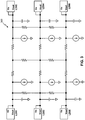
- FIG. 3 shows a topology 300 with an example of six adaptive bias and compensation LDO regulators, illustrated with abbreviated labels LDO1, LDO2 ... LDO6, connected in parallel and showing parasitic elements (shown but not separately labeled) of the power distribution network that interconnects them.
- LDO1, LDO2 ... LDO6 is according to the FIG. 2 example reduced SSR LDO regulator 200.
- each of the LOD regulators LDO1, LDO2 ... LDO6 has a Vref input (not shown) and that each Vref input is connected to Vref source (not shown).
- At least one Vref source may be shared by two or more of the adaptive bias and compensation LDO regulators LDO1, LDO2 ... LDO6. It will be understood that the FIG. 3 capacitors (shown but not separately labeled) may represent explicitly placed load capacitances as well as parasitic capacitances.
- FIG. 4 illustrates an exemplary wireless communication system 400 in which one or more embodiments of the disclosure may be advantageously employed.
- FIG. 4 shows three remote units 420, 430, and 450 and two base stations 440. It will be recognized that conventional wireless communication systems may have many more remote units and base stations.
- the remote units 420, 430, and 450 include integrated circuit or other semiconductor devices 425, 435 and 455 (including on-chip voltage regulators, as disclosed herein), which are among embodiments of the disclosure as discussed further below.
- FIG. 4 shows forward link signals 480 from the base stations 440 and the remote units 420, 430, and 450 and reverse link signals 490 from the remote units 420, 430, and 450 to the base stations 440.
- the remote unit 420 is shown as a mobile telephone
- the remote unit 430 is shown as a portable computer
- the remote unit 450 is shown as a fixed location remote unit in a wireless local loop system.
- the remote units may be any one or combination of a mobile phone, hand-held personal communication system (PCS) unit, portable data unit such as a personal data assistant (PDA), navigation device (such as GPS enabled devices), set top box, music player, video player, entertainment unit, fixed location data unit such as meter reading equipment, or any other device that stores or retrieves data or computer instructions, or any combination thereof.
- FIG. 4 illustrates remote units according to the teachings of the disclosure, the disclosure is not limited to these exemplary illustrated units. Embodiments of the disclosure may be suitably employed in any device having active integrated circuitry including memory and on-chip circuitry for test and characterization.
- the foregoing disclosed devices and functionalities may be designed and configured into computer files (e.g., RTL, GDSII, GERBER, etc.) stored on computer readable media. Some or all such files may be provided to fabrication handlers who fabricate devices based on such files. Resulting products include semiconductor wafers that are then cut into semiconductor die and packaged into a semiconductor chip. The semiconductor chips can be employed in electronic devices, such as described hereinabove.
- computer files e.g., RTL, GDSII, GERBER, etc.
- Some or all such files may be provided to fabrication handlers who fabricate devices based on such files.
- Resulting products include semiconductor wafers that are then cut into semiconductor die and packaged into a semiconductor chip.
- the semiconductor chips can be employed in electronic devices, such as described hereinabove.
- a software module may reside in RAM memory, flash memory, ROM memory, EPROM memory, EEPROM memory, registers, hard disk, a removable disk, a CD-ROM, or any other form of storage medium known in the art.
- An exemplary storage medium is coupled to the processor such that the processor can read information from, and write information to, the storage medium. In the alternative, the storage medium may be integral to the processor.
- an embodiment of the invention can include a computer readable media embodying a method for implementation. Accordingly, the invention is not limited to illustrated examples and any means for performing the functionality described herein are included in embodiments of the invention.
- the foregoing disclosed devices and functionalities may be designed and configured into computer files (e.g. RTL, GDSII, GERBER, etc.) stored on computer readable media. Some or all such files may be provided to fabrication handlers who fabricate devices based on such files. Resulting products include semiconductor wafers that are then cut into semiconductor die and packaged into a semiconductor chip. The chips are then employed in devices described above.
- computer files e.g. RTL, GDSII, GERBER, etc.
Landscapes
- Engineering & Computer Science (AREA)
- Physics & Mathematics (AREA)
- Electromagnetism (AREA)
- General Physics & Mathematics (AREA)
- Radar, Positioning & Navigation (AREA)
- Automation & Control Theory (AREA)
- Multimedia (AREA)
- Signal Processing (AREA)
- Continuous-Control Power Sources That Use Transistors (AREA)
- Amplifiers (AREA)
Applications Claiming Priority (4)
| Application Number | Priority Date | Filing Date | Title |
|---|---|---|---|
| US201261722876P | 2012-11-06 | 2012-11-06 | |
| US13/788,115 US9235225B2 (en) | 2012-11-06 | 2013-03-07 | Method and apparatus reduced switch-on rate low dropout regulator (LDO) bias and compensation |
| EP13795635.5A EP2917800B1 (en) | 2012-11-06 | 2013-11-05 | Method and apparatus reduced switch-on rate low dropout regulator (ldo) bias and compensation |
| PCT/US2013/068522 WO2014074520A2 (en) | 2012-11-06 | 2013-11-05 | Method and apparatus reduced switch-on rate low dropout regulator (ldo) bias and compensation |
Related Parent Applications (2)
| Application Number | Title | Priority Date | Filing Date |
|---|---|---|---|
| EP13795635.5A Division EP2917800B1 (en) | 2012-11-06 | 2013-11-05 | Method and apparatus reduced switch-on rate low dropout regulator (ldo) bias and compensation |
| EP13795635.5A Division-Into EP2917800B1 (en) | 2012-11-06 | 2013-11-05 | Method and apparatus reduced switch-on rate low dropout regulator (ldo) bias and compensation |
Publications (2)
| Publication Number | Publication Date |
|---|---|
| EP3422135A1 EP3422135A1 (en) | 2019-01-02 |
| EP3422135B1 true EP3422135B1 (en) | 2021-03-24 |
Family
ID=50621759
Family Applications (2)
| Application Number | Title | Priority Date | Filing Date |
|---|---|---|---|
| EP18190338.6A Active EP3422135B1 (en) | 2012-11-06 | 2013-11-05 | Method and apparatus reduced switch-on rate low dropout regulator (ldo) bias and compensation |
| EP13795635.5A Active EP2917800B1 (en) | 2012-11-06 | 2013-11-05 | Method and apparatus reduced switch-on rate low dropout regulator (ldo) bias and compensation |
Family Applications After (1)
| Application Number | Title | Priority Date | Filing Date |
|---|---|---|---|
| EP13795635.5A Active EP2917800B1 (en) | 2012-11-06 | 2013-11-05 | Method and apparatus reduced switch-on rate low dropout regulator (ldo) bias and compensation |
Country Status (7)
Families Citing this family (19)
| Publication number | Priority date | Publication date | Assignee | Title |
|---|---|---|---|---|
| US9170590B2 (en) | 2012-10-31 | 2015-10-27 | Qualcomm Incorporated | Method and apparatus for load adaptive LDO bias and compensation |
| US9122293B2 (en) | 2012-10-31 | 2015-09-01 | Qualcomm Incorporated | Method and apparatus for LDO and distributed LDO transient response accelerator |
| US8981745B2 (en) | 2012-11-18 | 2015-03-17 | Qualcomm Incorporated | Method and apparatus for bypass mode low dropout (LDO) regulator |
| US11095216B2 (en) | 2014-05-30 | 2021-08-17 | Qualcomm Incorporated | On-chip dual-supply multi-mode CMOS regulators |
| CN104063003B (zh) * | 2014-06-27 | 2015-10-21 | 合肥工业大学 | 一种集成摆率增强电路的低功耗无片外电容ldo |
| US9563242B2 (en) * | 2014-08-28 | 2017-02-07 | Mediatek Inc. | Pulse width modulation based real-time clock system and associated method |
| TWI534584B (zh) * | 2015-05-20 | 2016-05-21 | 晶宏半導體股份有限公司 | 用於顯示器之自放電穩壓裝置 |
| KR102409919B1 (ko) | 2015-09-02 | 2022-06-16 | 삼성전자주식회사 | 레귤레이터 회로 및 이를 포함하는 전력 시스템 |
| US9933800B1 (en) | 2016-09-30 | 2018-04-03 | Synaptics Incorporated | Frequency compensation for linear regulators |
| CN110168894B (zh) * | 2017-08-16 | 2020-07-28 | 华为技术有限公司 | 一种调压电路 |
| US10013005B1 (en) * | 2017-08-31 | 2018-07-03 | Xilinx, Inc. | Low voltage regulator |
| JP6592126B2 (ja) | 2018-02-09 | 2019-10-16 | 華邦電子股▲ふん▼有限公司Winbond Electronics Corp. | ビット線電源供給装置 |
| KR20220010125A (ko) * | 2020-07-17 | 2022-01-25 | 에스케이하이닉스 주식회사 | 증폭기 및 이를 포함하는 전압 생성 회로 |
| CN112034924B (zh) * | 2020-08-10 | 2023-02-24 | 唯捷创芯(天津)电子技术股份有限公司 | 一种自适应快速响应的ldo电路及其芯片 |
| JP7391791B2 (ja) * | 2020-08-12 | 2023-12-05 | 株式会社東芝 | 定電圧回路 |
| CN112462834B (zh) * | 2020-10-27 | 2022-05-13 | 北京智芯微电子科技有限公司 | 用于快速唤醒芯片的电流偏置电路 |
| KR102609484B1 (ko) * | 2021-11-22 | 2023-12-01 | 고려대학교 산학협력단 | 연산 트랜스-컨덕턴스 증폭기를 사용하는 하이브리드 ldo 레귤레이터 |
| US12184175B2 (en) | 2022-11-16 | 2024-12-31 | Shanghai Dn Semiconductors Co., Ltd. | Voltage regulator with boost current control circuitry |
| US20240427409A1 (en) * | 2023-06-20 | 2024-12-26 | Qualcomm Incorporated | Electrical device with a deep sleep mode implemented with a level shifter |
Family Cites Families (59)
| Publication number | Priority date | Publication date | Assignee | Title |
|---|---|---|---|---|
| US4656647A (en) | 1985-05-17 | 1987-04-07 | William Hotine | Pulsed bi-phase digital modulator system |
| JP2785732B2 (ja) | 1995-02-08 | 1998-08-13 | 日本電気株式会社 | 電源降圧回路 |
| US6046577A (en) | 1997-01-02 | 2000-04-04 | Texas Instruments Incorporated | Low-dropout voltage regulator incorporating a current efficient transient response boost circuit |
| US5982226A (en) | 1997-04-07 | 1999-11-09 | Texas Instruments Incorporated | Optimized frequency shaping circuit topologies for LDOs |
| JPH11231954A (ja) * | 1998-02-16 | 1999-08-27 | Mitsubishi Electric Corp | 内部電源電圧発生回路 |
| US6031417A (en) | 1998-04-01 | 2000-02-29 | Rockwell International | Differential amplifier for multiple supply voltages and biasing device therefore |
| US6188211B1 (en) | 1998-05-13 | 2001-02-13 | Texas Instruments Incorporated | Current-efficient low-drop-out voltage regulator with improved load regulation and frequency response |
| JP4472069B2 (ja) | 1999-11-10 | 2010-06-02 | オリンパス株式会社 | 医療用カプセル内視鏡 |
| US6188212B1 (en) | 2000-04-28 | 2001-02-13 | Burr-Brown Corporation | Low dropout voltage regulator circuit including gate offset servo circuit powered by charge pump |
| US6373233B2 (en) * | 2000-07-17 | 2002-04-16 | Philips Electronics No. America Corp. | Low-dropout voltage regulator with improved stability for all capacitive loads |
| US6246221B1 (en) | 2000-09-20 | 2001-06-12 | Texas Instruments Incorporated | PMOS low drop-out voltage regulator using non-inverting variable gain stage |
| US6333623B1 (en) | 2000-10-30 | 2001-12-25 | Texas Instruments Incorporated | Complementary follower output stage circuitry and method for low dropout voltage regulator |
| US6522111B2 (en) | 2001-01-26 | 2003-02-18 | Linfinity Microelectronics | Linear voltage regulator using adaptive biasing |
| US6518737B1 (en) | 2001-09-28 | 2003-02-11 | Catalyst Semiconductor, Inc. | Low dropout voltage regulator with non-miller frequency compensation |
| US6703815B2 (en) | 2002-05-20 | 2004-03-09 | Texas Instruments Incorporated | Low drop-out regulator having current feedback amplifier and composite feedback loop |
| US6617833B1 (en) * | 2002-04-01 | 2003-09-09 | Texas Instruments Incorporated | Self-initialized soft start for Miller compensated regulators |
| KR100528789B1 (ko) * | 2003-08-01 | 2005-11-15 | 주식회사 하이닉스반도체 | 셀프 리프래쉬 모드 진입을 위한 클럭 인에이블 버퍼 |
| US6879142B2 (en) | 2003-08-20 | 2005-04-12 | Broadcom Corporation | Power management unit for use in portable applications |
| JP2005205072A (ja) | 2004-01-26 | 2005-08-04 | Olympus Corp | カプセル型医療装置 |
| US7368896B2 (en) | 2004-03-29 | 2008-05-06 | Ricoh Company, Ltd. | Voltage regulator with plural error amplifiers |
| US7091710B2 (en) | 2004-05-03 | 2006-08-15 | System General Corp. | Low dropout voltage regulator providing adaptive compensation |
| EP1635239A1 (en) | 2004-09-14 | 2006-03-15 | Dialog Semiconductor GmbH | Adaptive biasing concept for current mode voltage regulators |
| TWI263124B (en) * | 2004-11-19 | 2006-10-01 | Sunplus Technology Co Ltd | Voltage regulator circuit with low quiescent current |
| US7215103B1 (en) | 2004-12-22 | 2007-05-08 | National Semiconductor Corporation | Power conservation by reducing quiescent current in low power and standby modes |
| JP2006230680A (ja) | 2005-02-24 | 2006-09-07 | Pentax Corp | カプセル型医療機器 |
| JP4523473B2 (ja) | 2005-04-04 | 2010-08-11 | 株式会社リコー | 定電圧回路 |
| DE102005015522A1 (de) | 2005-04-04 | 2006-10-05 | Karl Storz Gmbh & Co. Kg | Intrakorporale Videokapsel mit schwenkbarem Bildaufnehmer |
| JP4695432B2 (ja) | 2005-04-12 | 2011-06-08 | オリンパスメディカルシステムズ株式会社 | 被検体内導入装置、被検体内情報表示装置、及び被検体内情報取得システム |
| DE102005039114B4 (de) | 2005-08-18 | 2007-06-28 | Texas Instruments Deutschland Gmbh | Spannungsregler mit einem geringen Spannungsabfall |
| FR2896051B1 (fr) | 2006-01-09 | 2008-04-18 | St Microelectronics Sa | Regulateur de tension serie a faible tension d'insertion |
| JP2007280025A (ja) | 2006-04-06 | 2007-10-25 | Seiko Epson Corp | 電源装置 |
| EP1865397B1 (en) | 2006-06-05 | 2012-11-21 | St Microelectronics S.A. | Low drop-out voltage regulator |
| JP4653046B2 (ja) * | 2006-09-08 | 2011-03-16 | 株式会社リコー | 差動増幅回路、差動増幅回路を使用したボルテージレギュレータ及び差動増幅回路の動作制御方法 |
| JP4914738B2 (ja) * | 2007-02-17 | 2012-04-11 | セイコーインスツル株式会社 | ボルテージレギュレータ |
| US7728569B1 (en) | 2007-04-10 | 2010-06-01 | Altera Corporation | Voltage regulator circuitry with adaptive compensation |
| CN100495281C (zh) * | 2007-09-07 | 2009-06-03 | 北京时代民芯科技有限公司 | 一种低压差线性稳压器 |
| JP4937865B2 (ja) | 2007-09-11 | 2012-05-23 | 株式会社リコー | 定電圧回路 |
| KR100924293B1 (ko) | 2007-09-14 | 2009-10-30 | 한국과학기술원 | 저전압 강하 레귤레이터 |
| US7804415B2 (en) | 2007-09-14 | 2010-09-28 | Astec International Limited | Health monitoring for power converter components |
| US8072196B1 (en) | 2008-01-15 | 2011-12-06 | National Semiconductor Corporation | System and method for providing a dynamically configured low drop out regulator with zero quiescent current and fast transient response |
| JP5035987B2 (ja) | 2008-01-28 | 2012-09-26 | 富士フイルム株式会社 | カプセル内視鏡、およびカプセル内視鏡の動作制御方法 |
| US7768351B2 (en) | 2008-06-25 | 2010-08-03 | Texas Instruments Incorporated | Variable gain current input amplifier and method |
| JP5112208B2 (ja) * | 2008-07-18 | 2013-01-09 | ルネサスエレクトロニクス株式会社 | レギュレータ及び半導体装置 |
| US8080983B2 (en) | 2008-11-03 | 2011-12-20 | Microchip Technology Incorporated | Low drop out (LDO) bypass voltage regulator |
| US8305056B2 (en) * | 2008-12-09 | 2012-11-06 | Qualcomm Incorporated | Low drop-out voltage regulator with wide bandwidth power supply rejection ratio |
| IT1392263B1 (it) | 2008-12-15 | 2012-02-22 | St Microelectronics Des & Appl | Regolatore lineare di tipo low-dropout e corrispondente procedimento |
| KR101530085B1 (ko) * | 2008-12-24 | 2015-06-18 | 테세라 어드밴스드 테크놀로지스, 인크. | 저 드롭 아웃(ldo) 전압 레귤레이터 및 그의 동작 방법 |
| CN102117089B (zh) | 2009-12-31 | 2013-04-17 | 财团法人工业技术研究院 | 低压降稳压器 |
| KR101094401B1 (ko) | 2010-03-31 | 2011-12-15 | 주식회사 하이닉스반도체 | 반도체 집적회로의 내부전압 발생기 |
| US8169203B1 (en) | 2010-11-19 | 2012-05-01 | Nxp B.V. | Low dropout regulator |
| US8471539B2 (en) * | 2010-12-23 | 2013-06-25 | Winbond Electronics Corp. | Low drop out voltage regulato |
| US8344713B2 (en) | 2011-01-11 | 2013-01-01 | Freescale Semiconductor, Inc. | LDO linear regulator with improved transient response |
| WO2012104673A1 (en) | 2011-01-31 | 2012-08-09 | Freescale Semiconductor, Inc. | Integrated circuit device, voltage regulation circuitry and method for regulating a voltage supply signal |
| US20120212199A1 (en) | 2011-02-22 | 2012-08-23 | Ahmed Amer | Low Drop Out Voltage Regulator |
| EP2498161B1 (en) | 2011-03-07 | 2020-02-19 | Dialog Semiconductor GmbH | Power efficient generation of band gap referenced supply rail, voltage and current references, and method for dynamic control. |
| CN102279612A (zh) * | 2011-05-11 | 2011-12-14 | 电子科技大学 | 一种低压差线性稳压器 |
| US9170590B2 (en) | 2012-10-31 | 2015-10-27 | Qualcomm Incorporated | Method and apparatus for load adaptive LDO bias and compensation |
| US9122293B2 (en) | 2012-10-31 | 2015-09-01 | Qualcomm Incorporated | Method and apparatus for LDO and distributed LDO transient response accelerator |
| US8981745B2 (en) | 2012-11-18 | 2015-03-17 | Qualcomm Incorporated | Method and apparatus for bypass mode low dropout (LDO) regulator |
-
2013
- 2013-03-07 US US13/788,115 patent/US9235225B2/en active Active
- 2013-11-05 WO PCT/US2013/068522 patent/WO2014074520A2/en active Application Filing
- 2013-11-05 EP EP18190338.6A patent/EP3422135B1/en active Active
- 2013-11-05 ES ES18190338T patent/ES2870226T3/es active Active
- 2013-11-05 EP EP13795635.5A patent/EP2917800B1/en active Active
- 2013-11-05 ES ES13795635T patent/ES2701998T3/es active Active
- 2013-11-05 CN CN201380055425.6A patent/CN104756032B/zh active Active
- 2013-11-05 HU HUE13795635A patent/HUE040259T2/hu unknown
- 2013-11-05 JP JP2015540867A patent/JP6465804B2/ja active Active
-
2018
- 2018-11-21 JP JP2018218136A patent/JP6724112B2/ja active Active
Non-Patent Citations (1)
| Title |
|---|
| None * |
Also Published As
| Publication number | Publication date |
|---|---|
| ES2870226T3 (es) | 2021-10-26 |
| JP2019053757A (ja) | 2019-04-04 |
| WO2014074520A2 (en) | 2014-05-15 |
| US20140125300A1 (en) | 2014-05-08 |
| EP2917800B1 (en) | 2018-09-26 |
| WO2014074520A3 (en) | 2014-08-14 |
| CN104756032B (zh) | 2016-11-09 |
| ES2701998T3 (es) | 2019-02-26 |
| HUE040259T2 (hu) | 2019-02-28 |
| JP6465804B2 (ja) | 2019-02-06 |
| EP2917800A2 (en) | 2015-09-16 |
| US9235225B2 (en) | 2016-01-12 |
| JP2015533443A (ja) | 2015-11-24 |
| JP6724112B2 (ja) | 2020-07-15 |
| CN104756032A (zh) | 2015-07-01 |
| EP3422135A1 (en) | 2019-01-02 |
Similar Documents
| Publication | Publication Date | Title |
|---|---|---|
| EP3422135B1 (en) | Method and apparatus reduced switch-on rate low dropout regulator (ldo) bias and compensation | |
| US8981745B2 (en) | Method and apparatus for bypass mode low dropout (LDO) regulator | |
| US9170590B2 (en) | Method and apparatus for load adaptive LDO bias and compensation | |
| EP3423915B1 (en) | Multiple input multiple output regulator controller system | |
| US9122293B2 (en) | Method and apparatus for LDO and distributed LDO transient response accelerator | |
| KR102040692B1 (ko) | 공급 전압을 안정화시키기 위한 디바이스 및 방법 | |
| US8866341B2 (en) | Voltage regulator | |
| CN110383202B (zh) | 可编程电源发生器 | |
| US20140159683A1 (en) | Settling Time and Effective Band Width for Op-Amps Using Miller Capacitance Compensation | |
| US9831762B2 (en) | Apparatus for starting up switching voltage regulator | |
| CN105009435A (zh) | 用于电流模式迟滞降压调节器的前馈频率控制方法 | |
| KR20120136449A (ko) | 소프트 스타트 회로의 동작 방법과 상기 방법을 수행할 수 있는 장치들 | |
| CN106843348A (zh) | 电压调节器和包括该电压调节器的移动设备 | |
| US20140002045A1 (en) | Analog circuit configured for fast, accurate startup |
Legal Events
| Date | Code | Title | Description |
|---|---|---|---|
| PUAI | Public reference made under article 153(3) epc to a published international application that has entered the european phase |
Free format text: ORIGINAL CODE: 0009012 |
|
| STAA | Information on the status of an ep patent application or granted ep patent |
Free format text: STATUS: REQUEST FOR EXAMINATION WAS MADE |
|
| 17P | Request for examination filed |
Effective date: 20180822 |
|
| AC | Divisional application: reference to earlier application |
Ref document number: 2917800 Country of ref document: EP Kind code of ref document: P |
|
| AK | Designated contracting states |
Kind code of ref document: A1 Designated state(s): AL AT BE BG CH CY CZ DE DK EE ES FI FR GB GR HR HU IE IS IT LI LT LU LV MC MK MT NL NO PL PT RO RS SE SI SK SM TR |
|
| GRAP | Despatch of communication of intention to grant a patent |
Free format text: ORIGINAL CODE: EPIDOSNIGR1 |
|
| STAA | Information on the status of an ep patent application or granted ep patent |
Free format text: STATUS: GRANT OF PATENT IS INTENDED |
|
| RIC1 | Information provided on ipc code assigned before grant |
Ipc: G05F 1/46 20060101ALI20201023BHEP Ipc: G05F 1/575 20060101AFI20201023BHEP |
|
| INTG | Intention to grant announced |
Effective date: 20201113 |
|
| GRAS | Grant fee paid |
Free format text: ORIGINAL CODE: EPIDOSNIGR3 |
|
| GRAA | (expected) grant |
Free format text: ORIGINAL CODE: 0009210 |
|
| STAA | Information on the status of an ep patent application or granted ep patent |
Free format text: STATUS: THE PATENT HAS BEEN GRANTED |
|
| AC | Divisional application: reference to earlier application |
Ref document number: 2917800 Country of ref document: EP Kind code of ref document: P |
|
| AK | Designated contracting states |
Kind code of ref document: B1 Designated state(s): AL AT BE BG CH CY CZ DE DK EE ES FI FR GB GR HR HU IE IS IT LI LT LU LV MC MK MT NL NO PL PT RO RS SE SI SK SM TR |
|
| REG | Reference to a national code |
Ref country code: GB Ref legal event code: FG4D |
|
| REG | Reference to a national code |
Ref country code: CH Ref legal event code: EP |
|
| REG | Reference to a national code |
Ref country code: IE Ref legal event code: FG4D |
|
| REG | Reference to a national code |
Ref country code: DE Ref legal event code: R096 Ref document number: 602013076520 Country of ref document: DE Ref country code: AT Ref legal event code: REF Ref document number: 1375128 Country of ref document: AT Kind code of ref document: T Effective date: 20210415 |
|
| REG | Reference to a national code |
Ref country code: NL Ref legal event code: FP |
|
| REG | Reference to a national code |
Ref country code: SE Ref legal event code: TRGR |
|
| REG | Reference to a national code |
Ref country code: LT Ref legal event code: MG9D |
|
| PG25 | Lapsed in a contracting state [announced via postgrant information from national office to epo] |
Ref country code: BG Free format text: LAPSE BECAUSE OF FAILURE TO SUBMIT A TRANSLATION OF THE DESCRIPTION OR TO PAY THE FEE WITHIN THE PRESCRIBED TIME-LIMIT Effective date: 20210624 Ref country code: FI Free format text: LAPSE BECAUSE OF FAILURE TO SUBMIT A TRANSLATION OF THE DESCRIPTION OR TO PAY THE FEE WITHIN THE PRESCRIBED TIME-LIMIT Effective date: 20210324 Ref country code: GR Free format text: LAPSE BECAUSE OF FAILURE TO SUBMIT A TRANSLATION OF THE DESCRIPTION OR TO PAY THE FEE WITHIN THE PRESCRIBED TIME-LIMIT Effective date: 20210625 Ref country code: HR Free format text: LAPSE BECAUSE OF FAILURE TO SUBMIT A TRANSLATION OF THE DESCRIPTION OR TO PAY THE FEE WITHIN THE PRESCRIBED TIME-LIMIT Effective date: 20210324 Ref country code: NO Free format text: LAPSE BECAUSE OF FAILURE TO SUBMIT A TRANSLATION OF THE DESCRIPTION OR TO PAY THE FEE WITHIN THE PRESCRIBED TIME-LIMIT Effective date: 20210624 |
|
| PG25 | Lapsed in a contracting state [announced via postgrant information from national office to epo] |
Ref country code: LV Free format text: LAPSE BECAUSE OF FAILURE TO SUBMIT A TRANSLATION OF THE DESCRIPTION OR TO PAY THE FEE WITHIN THE PRESCRIBED TIME-LIMIT Effective date: 20210324 Ref country code: RS Free format text: LAPSE BECAUSE OF FAILURE TO SUBMIT A TRANSLATION OF THE DESCRIPTION OR TO PAY THE FEE WITHIN THE PRESCRIBED TIME-LIMIT Effective date: 20210324 |
|
| REG | Reference to a national code |
Ref country code: AT Ref legal event code: MK05 Ref document number: 1375128 Country of ref document: AT Kind code of ref document: T Effective date: 20210324 |
|
| REG | Reference to a national code |
Ref country code: ES Ref legal event code: FG2A Ref document number: 2870226 Country of ref document: ES Kind code of ref document: T3 Effective date: 20211026 |
|
| PG25 | Lapsed in a contracting state [announced via postgrant information from national office to epo] |
Ref country code: LT Free format text: LAPSE BECAUSE OF FAILURE TO SUBMIT A TRANSLATION OF THE DESCRIPTION OR TO PAY THE FEE WITHIN THE PRESCRIBED TIME-LIMIT Effective date: 20210324 Ref country code: EE Free format text: LAPSE BECAUSE OF FAILURE TO SUBMIT A TRANSLATION OF THE DESCRIPTION OR TO PAY THE FEE WITHIN THE PRESCRIBED TIME-LIMIT Effective date: 20210324 Ref country code: CZ Free format text: LAPSE BECAUSE OF FAILURE TO SUBMIT A TRANSLATION OF THE DESCRIPTION OR TO PAY THE FEE WITHIN THE PRESCRIBED TIME-LIMIT Effective date: 20210324 Ref country code: SM Free format text: LAPSE BECAUSE OF FAILURE TO SUBMIT A TRANSLATION OF THE DESCRIPTION OR TO PAY THE FEE WITHIN THE PRESCRIBED TIME-LIMIT Effective date: 20210324 Ref country code: AT Free format text: LAPSE BECAUSE OF FAILURE TO SUBMIT A TRANSLATION OF THE DESCRIPTION OR TO PAY THE FEE WITHIN THE PRESCRIBED TIME-LIMIT Effective date: 20210324 |
|
| PG25 | Lapsed in a contracting state [announced via postgrant information from national office to epo] |
Ref country code: PT Free format text: LAPSE BECAUSE OF FAILURE TO SUBMIT A TRANSLATION OF THE DESCRIPTION OR TO PAY THE FEE WITHIN THE PRESCRIBED TIME-LIMIT Effective date: 20210726 Ref country code: PL Free format text: LAPSE BECAUSE OF FAILURE TO SUBMIT A TRANSLATION OF THE DESCRIPTION OR TO PAY THE FEE WITHIN THE PRESCRIBED TIME-LIMIT Effective date: 20210324 Ref country code: RO Free format text: LAPSE BECAUSE OF FAILURE TO SUBMIT A TRANSLATION OF THE DESCRIPTION OR TO PAY THE FEE WITHIN THE PRESCRIBED TIME-LIMIT Effective date: 20210324 Ref country code: SK Free format text: LAPSE BECAUSE OF FAILURE TO SUBMIT A TRANSLATION OF THE DESCRIPTION OR TO PAY THE FEE WITHIN THE PRESCRIBED TIME-LIMIT Effective date: 20210324 Ref country code: IS Free format text: LAPSE BECAUSE OF FAILURE TO SUBMIT A TRANSLATION OF THE DESCRIPTION OR TO PAY THE FEE WITHIN THE PRESCRIBED TIME-LIMIT Effective date: 20210724 |
|
| REG | Reference to a national code |
Ref country code: DE Ref legal event code: R097 Ref document number: 602013076520 Country of ref document: DE |
|
| PG25 | Lapsed in a contracting state [announced via postgrant information from national office to epo] |
Ref country code: DK Free format text: LAPSE BECAUSE OF FAILURE TO SUBMIT A TRANSLATION OF THE DESCRIPTION OR TO PAY THE FEE WITHIN THE PRESCRIBED TIME-LIMIT Effective date: 20210324 Ref country code: AL Free format text: LAPSE BECAUSE OF FAILURE TO SUBMIT A TRANSLATION OF THE DESCRIPTION OR TO PAY THE FEE WITHIN THE PRESCRIBED TIME-LIMIT Effective date: 20210324 |
|
| PLBE | No opposition filed within time limit |
Free format text: ORIGINAL CODE: 0009261 |
|
| STAA | Information on the status of an ep patent application or granted ep patent |
Free format text: STATUS: NO OPPOSITION FILED WITHIN TIME LIMIT |
|
| PG25 | Lapsed in a contracting state [announced via postgrant information from national office to epo] |
Ref country code: SI Free format text: LAPSE BECAUSE OF FAILURE TO SUBMIT A TRANSLATION OF THE DESCRIPTION OR TO PAY THE FEE WITHIN THE PRESCRIBED TIME-LIMIT Effective date: 20210324 |
|
| 26N | No opposition filed |
Effective date: 20220104 |
|
| PG25 | Lapsed in a contracting state [announced via postgrant information from national office to epo] |
Ref country code: IS Free format text: LAPSE BECAUSE OF FAILURE TO SUBMIT A TRANSLATION OF THE DESCRIPTION OR TO PAY THE FEE WITHIN THE PRESCRIBED TIME-LIMIT Effective date: 20210724 |
|
| PG25 | Lapsed in a contracting state [announced via postgrant information from national office to epo] |
Ref country code: MC Free format text: LAPSE BECAUSE OF FAILURE TO SUBMIT A TRANSLATION OF THE DESCRIPTION OR TO PAY THE FEE WITHIN THE PRESCRIBED TIME-LIMIT Effective date: 20210324 |
|
| PG25 | Lapsed in a contracting state [announced via postgrant information from national office to epo] |
Ref country code: LU Free format text: LAPSE BECAUSE OF NON-PAYMENT OF DUE FEES Effective date: 20211105 Ref country code: BE Free format text: LAPSE BECAUSE OF NON-PAYMENT OF DUE FEES Effective date: 20211130 |
|
| REG | Reference to a national code |
Ref country code: BE Ref legal event code: MM Effective date: 20211130 |
|
| PG25 | Lapsed in a contracting state [announced via postgrant information from national office to epo] |
Ref country code: IE Free format text: LAPSE BECAUSE OF NON-PAYMENT OF DUE FEES Effective date: 20211105 |
|
| PG25 | Lapsed in a contracting state [announced via postgrant information from national office to epo] |
Ref country code: CY Free format text: LAPSE BECAUSE OF FAILURE TO SUBMIT A TRANSLATION OF THE DESCRIPTION OR TO PAY THE FEE WITHIN THE PRESCRIBED TIME-LIMIT Effective date: 20210324 |
|
| PG25 | Lapsed in a contracting state [announced via postgrant information from national office to epo] |
Ref country code: HU Free format text: LAPSE BECAUSE OF FAILURE TO SUBMIT A TRANSLATION OF THE DESCRIPTION OR TO PAY THE FEE WITHIN THE PRESCRIBED TIME-LIMIT; INVALID AB INITIO Effective date: 20131105 |
|
| PG25 | Lapsed in a contracting state [announced via postgrant information from national office to epo] |
Ref country code: MK Free format text: LAPSE BECAUSE OF FAILURE TO SUBMIT A TRANSLATION OF THE DESCRIPTION OR TO PAY THE FEE WITHIN THE PRESCRIBED TIME-LIMIT Effective date: 20210324 |
|
| PG25 | Lapsed in a contracting state [announced via postgrant information from national office to epo] |
Ref country code: TR Free format text: LAPSE BECAUSE OF FAILURE TO SUBMIT A TRANSLATION OF THE DESCRIPTION OR TO PAY THE FEE WITHIN THE PRESCRIBED TIME-LIMIT Effective date: 20210324 |
|
| PG25 | Lapsed in a contracting state [announced via postgrant information from national office to epo] |
Ref country code: MT Free format text: LAPSE BECAUSE OF FAILURE TO SUBMIT A TRANSLATION OF THE DESCRIPTION OR TO PAY THE FEE WITHIN THE PRESCRIBED TIME-LIMIT Effective date: 20210324 |
|
| PGFP | Annual fee paid to national office [announced via postgrant information from national office to epo] |
Ref country code: NL Payment date: 20241014 Year of fee payment: 12 |
|
| PGFP | Annual fee paid to national office [announced via postgrant information from national office to epo] |
Ref country code: DE Payment date: 20241010 Year of fee payment: 12 |
|
| PGFP | Annual fee paid to national office [announced via postgrant information from national office to epo] |
Ref country code: GB Payment date: 20241010 Year of fee payment: 12 |
|
| PGFP | Annual fee paid to national office [announced via postgrant information from national office to epo] |
Ref country code: FR Payment date: 20241010 Year of fee payment: 12 |
|
| PGFP | Annual fee paid to national office [announced via postgrant information from national office to epo] |
Ref country code: IT Payment date: 20241111 Year of fee payment: 12 Ref country code: ES Payment date: 20241212 Year of fee payment: 12 |
|
| PGFP | Annual fee paid to national office [announced via postgrant information from national office to epo] |
Ref country code: SE Payment date: 20241108 Year of fee payment: 12 |
|
| PGFP | Annual fee paid to national office [announced via postgrant information from national office to epo] |
Ref country code: CH Payment date: 20241201 Year of fee payment: 12 |