EP2917800B1 - Method and apparatus reduced switch-on rate low dropout regulator (ldo) bias and compensation - Google Patents
Method and apparatus reduced switch-on rate low dropout regulator (ldo) bias and compensation Download PDFInfo
- Publication number
- EP2917800B1 EP2917800B1 EP13795635.5A EP13795635A EP2917800B1 EP 2917800 B1 EP2917800 B1 EP 2917800B1 EP 13795635 A EP13795635 A EP 13795635A EP 2917800 B1 EP2917800 B1 EP 2917800B1
- Authority
- EP
- European Patent Office
- Prior art keywords
- slew
- bias current
- switch
- pass gate
- full
- Prior art date
- Legal status (The legal status is an assumption and is not a legal conclusion. Google has not performed a legal analysis and makes no representation as to the accuracy of the status listed.)
- Active
Links
- 238000000034 method Methods 0.000 title claims description 17
- 230000007704 transition Effects 0.000 claims description 41
- 239000003990 capacitor Substances 0.000 claims description 35
- 230000004044 response Effects 0.000 claims description 31
- 230000001105 regulatory effect Effects 0.000 claims description 8
- 230000008878 coupling Effects 0.000 claims description 5
- 238000010168 coupling process Methods 0.000 claims description 5
- 238000005859 coupling reaction Methods 0.000 claims description 5
- 230000003111 delayed effect Effects 0.000 claims description 4
- 238000012358 sourcing Methods 0.000 claims 2
- 230000001276 controlling effect Effects 0.000 claims 1
- 239000004065 semiconductor Substances 0.000 description 8
- 238000004891 communication Methods 0.000 description 4
- 230000006870 function Effects 0.000 description 4
- 238000003860 storage Methods 0.000 description 4
- 230000003044 adaptive effect Effects 0.000 description 3
- 238000007796 conventional method Methods 0.000 description 3
- 238000009826 distribution Methods 0.000 description 3
- 230000000694 effects Effects 0.000 description 3
- 230000003071 parasitic effect Effects 0.000 description 3
- 230000009471 action Effects 0.000 description 2
- 230000008901 benefit Effects 0.000 description 2
- 238000005516 engineering process Methods 0.000 description 2
- 238000004519 manufacturing process Methods 0.000 description 2
- 230000004048 modification Effects 0.000 description 2
- 238000012986 modification Methods 0.000 description 2
- 239000002245 particle Substances 0.000 description 2
- 230000009467 reduction Effects 0.000 description 2
- 235000012431 wafers Nutrition 0.000 description 2
- 230000008859 change Effects 0.000 description 1
- 238000012512 characterization method Methods 0.000 description 1
- 238000013461 design Methods 0.000 description 1
- 238000010586 diagram Methods 0.000 description 1
- 238000007599 discharging Methods 0.000 description 1
- 230000020169 heat generation Effects 0.000 description 1
- 230000008676 import Effects 0.000 description 1
- 230000007246 mechanism Effects 0.000 description 1
- 230000003287 optical effect Effects 0.000 description 1
- 230000003334 potential effect Effects 0.000 description 1
- 230000008569 process Effects 0.000 description 1
- 238000012360 testing method Methods 0.000 description 1
Images

Classifications
-
- G—PHYSICS
- G05—CONTROLLING; REGULATING
- G05F—SYSTEMS FOR REGULATING ELECTRIC OR MAGNETIC VARIABLES
- G05F1/00—Automatic systems in which deviations of an electric quantity from one or more predetermined values are detected at the output of the system and fed back to a device within the system to restore the detected quantity to its predetermined value or values, i.e. retroactive systems
- G05F1/10—Regulating voltage or current
- G05F1/46—Regulating voltage or current wherein the variable actually regulated by the final control device is dc
- G05F1/468—Regulating voltage or current wherein the variable actually regulated by the final control device is dc characterised by reference voltage circuitry, e.g. soft start, remote shutdown
-
- G—PHYSICS
- G05—CONTROLLING; REGULATING
- G05F—SYSTEMS FOR REGULATING ELECTRIC OR MAGNETIC VARIABLES
- G05F1/00—Automatic systems in which deviations of an electric quantity from one or more predetermined values are detected at the output of the system and fed back to a device within the system to restore the detected quantity to its predetermined value or values, i.e. retroactive systems
- G05F1/10—Regulating voltage or current
- G05F1/46—Regulating voltage or current wherein the variable actually regulated by the final control device is dc
- G05F1/56—Regulating voltage or current wherein the variable actually regulated by the final control device is dc using semiconductor devices in series with the load as final control devices
- G05F1/575—Regulating voltage or current wherein the variable actually regulated by the final control device is dc using semiconductor devices in series with the load as final control devices characterised by the feedback circuit
Definitions
- the technical field of the disclosure relates to voltage regulators and, more particularly, to low dropout (LDO) regulators.
- LDO low dropout
- An LDO regulator is a direct current (DC) linear voltage regulator that can operate with a very low dropout, where "dropout” (also termed “dropout voltage”) means the difference between the input voltage (e.g., received power supply rail voltage) and the regulated out voltage.
- dropout voltage also termed “dropout voltage”
- a low dropout voltage may provide, for example, higher efficiency and concomitant reduction in heat generation, as well as lower minimum operating voltage.
- US 2008/061881 discloses a type of voltage regulator.
- US 2006/0108993 discloses a regulator with low quiescent current.
- One example reduced switch-on slew LDO regulator can include a pass gate controllably coupling, in response to a pass gate control signal, a voltage rail to a regulator output.
- the pass gate control signal is generated by a controllable slew differential amplifier, switchable between a slew-limiting state and a full-slew state.
- the controllable slew differential amplifier is configured to receive a feedback from the regulator output, and to generate the pass gate control signal, based on a reference voltage and the feedback, at a full-slew rate in the full-slew state, and at a reduced slew rate in the slew-limiting state.
- One example reduced switch-on slew LDO regulator may further include a pass gate disabling circuit configured selectively over-ride the pass gate control signal and switch the pass gate OFF.
- controllable slew differential amplifier of one example reduced switch-on slew LDO regulator may include a switchable tail current source switchable between a slew-limiting bias current and a full-slew bias current.
- controllable slew differential amplifier may be configured to generate the pass gate control signal at the full-slew rate with the full-slew bias current, and at the reduced slew rate with the slew-limiting bias current.
- the switchable tail current source may include an ON-OFF switchable full-slew bias current source configured to source the full-slew bias current when ON, in parallel with a reduced slew bias current source configured to source the reduced slew bias current.
- One example reduced switch-on slew LDO regulator may further include, in an aspect, a tail current control circuit configured to switch the switchable tail current source to the slew-limiting bias current in response to an ON-to-OFF transition of a system ON-OFF signal (ST_ON/OFF).
- the tail current control circuit may be configured to switch the switchable tail current source, at a delay DLY after an OFF-to-ON transition of ST_OFF, from the slew-limiting bias current to the full-slew bias current.
- controllable slew differential amplifier may be configured to slew, in response to the OFF-to-ON transition of ST_ON/OFF, from an initial zero voltage to approximately Vref, at a reduced slew rate, in a time duration approximately equal to DLY.
- the tail current control circuit may include a delay capacitor, and a charging circuit configured to charge the delay capacitor, in response to the OFF-to-ON transition of ST_ON/OFF, from a zero voltage to a tail current source switching threshold voltage, in a charging time having a duration approximately equal to DLY.
- one example reduced switch-on slew LDO regulator may further include a pass gate control line carrying the pass gate control signal to a control gate of the pass gate.
- the pass gate disabling circuit may comprise a two-position switch, the two-position switch having a disabling position and an operational position, configured such that the disabling position provides a short of the control gate to a voltage disabling the pass gate, and the operational position does not provide the short of the control gate.
- the two-position switch may be configured to be movable, or to move, between the disabling position and the operational position based on an ON-OFF state of ST_OFF/ON.
- One example reduced switch-on slew LDO regulator may further include a feedback element that may be coupled to the regulator output and to an input of the differential amplifier to provide the feedback, and a compensation network coupling the pass gate control line to the feedback element.
- the compensation network may have a compensation capacitor and a compensation resistor, and the pass gate disabling circuit may be further configured to charge the compensation capacitor when the two-position switch is in the disabling position.
- the pass gate disabling circuit may be further configured to allow the compensation capacitor to discharge the pass gate control line, to a voltage at which the pass gate is operational, in response to switching the two-position switch from the disabling position to the operational position.
- a rate of the reduced slew rate may be based, at least in part, on at least one of a capacitance of the compensation capacitor or a resistance of the compensation resistor, or both.
- One example method may provide reduced switch-on slew low dropout (LDO) regulating with a pass gate controlled by a differential amplifier having differential inputs, and a transistor controlled by one of the differential inputs.
- Example methods may include biasing the transistor with a bias current, the biasing current being a full-slew bias current, and providing to the differential inputs a reference voltage and a feedback of an output of the pass gate.
- example methods may further provide, in response to an ON-to-OFF transition of a system on/off signal (ST_ON/OFF), disabling the feedback and switching the bias current to a slew-limiting bias current, lower than the full-slew bias current.
- ST_ON/OFF system on/off signal
- example methods may further include, in response to an OFF-to-ON transition of ST_ON/OFF, enabling the feedback to the differential amplifier and, at a time delayed from the OFF-to-ON transition by a reduced slew duration, switching the bias current to the full-slew bias current.
- the switching the biasing to bias the transistor with the full-slew bias current may include commencing, in response to the OFF-to-ON transition of ST_ON/OFF, a charging of a delay capacitor and, in response to the delay capacitor reaching a given threshold voltage level, performing the switching the biasing to bias the transistor with the full-slew bias current.
- One example reduced switch-on slew LDO regulator can include a differential amplifier having difference inputs, an output, and a transistor having a gate coupled to one of the difference inputs, in combination with a pass gate controlled by the output of the differential amplifier.
- the pass gate may include a pass gate input for coupling to a power rail, and a pass gate output, in further combination with means for receiving a system ON/OFF signal (ST_ON/OFF) and in response to an OFF-to-ON transition of ST_ON/OFF, establishing a feedback from the pass gate output to one of the difference inputs and biasing the transistor with a full-slew bias current, and in response to an ON-to-OFF transition of ST_ON/OFF, disabling the feedback and switching the biasing of the transistor to a slew-limiting bias current.
- ST_ON/OFF system ON/OFF signal
- topology refers to interconnections of circuit components and, unless stated otherwise, indicates nothing of physical layout of the components or their physical locations relative to one another. Figures described or otherwise identified as showing a topology are no more than a graphical representation of the topology and do not necessarily describe anything regarding physical layout or relative locations of components.
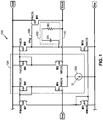
- FIG. 1 shows a topology for one example LDO regulator 100, having a differential amplifier 104 and a pass gate M9 that provides a controllable resistance (or conductance) coupling between an external power rail Vdd (hereinafter "Vdd rail”) and a regulated output voltage Vout terminal.
- Vdd rail external power rail
- the pass gate M9 is a PMOS transistor.
- the differential amplifier 104 receives as its differential inputs a reference voltage, Vref, and a feedback of Vout (over feedback element or feedback path 110).
- the differential amplifier 104 generates, based on the difference of Vref and the fed back Vout, a pass gate control signal at Vhg voltage (hereinafter referenced as "pass gate control signal Vhg") that is coupled, by pass gate control line 160, to the control gate (shown but not separately numbered) of the pass gate M9.
- pass gate control signal Vhg drives the resistance of pass gate M9 to a value at which Vout is, in this example, approximately equal to Vref.
- Vout being approximately equal to Vref is only for purposes of example.
- a voltage divider may be included to generate Vout higher than Vref.
- differential amplifier 104 is formed of two parallel branches (shown but not separately numbered) extending from the Vdd rail to a common node (shown but not separately numbered).
- a tail current source 106 sinks a bias current 15 from the common node to a reference rail Vss.
- One of the two branches comprises internal load transistor M5 in series with input transistor M4, the other comprises internal load transistor M6 in series with input transistor M2.
- the current 15 of the tail current source 106 sets the bias of the input transistors M2 and M4. 15 is fixed.
- the gate (shown but not separately numbered) of input transistor M4 functions as one of the differential amplifier 104 inputs (shown but not separately labeled), and receives Vref.
- the gate (shown but not separately labeled) of input transistor M2 receives functions as the other of the differential amplifier 104 inputs, by receiving Vout through the feedback path 110.
- the differential amplifier 104 inputs may be collectively referenced as the “differential inputs” or the “difference inputs.”
- transistors M3, M7, M8 and M10 form an intermediate buffer stage (shown but not separately numbered).
- the drain of M8 drives the pass gate control line 160 with the pass gate control signal Vhg.
- M8 may therefore be considered a drive transistor for the pass gate control signal Vhg.
- the feedback loop comprises the differential amplifier 104, the pass control drive transistor M8, the pass gate M9, the feedback path 110, and the Miller feedback compensation network 150.
- the Miller feedback compensation network 150 may be formed of resistor element R1 and capacitor element C1.
- the Miller feedback compensation network 150 produces a dominant pole along with a zero in the feedback response of the feedback loop, which provides stability.
- the general operation of Miller feedback compensation is known to persons of ordinary skill in the art and, therefore, further detailed description of the operation is omitted except where incidental to other described operation.
- a plurality of LDO regulators including, but not limited to the FIG. 1 example LDO regulator 100, may be used in providing regulated supply voltage within integrated circuit (IC) chips (not shown) having a plurality of circuit blocks (not shown), for example multiple processor cores.
- IC chips may include, in various applications, selective power-up features, for example, selective powering up and powering down individual circuit blocks, or subsets of the circuit blocks.
- the powering up of individual circuit blocks e.g., processor cores
- the powering up of individual circuit blocks includes simply switching on and off an LDO regulator such as the FIG. 1 example LDO regulator 100, a result may be large in-rush currents.
- the large in-rush currents may result in unwanted incidents of high rate current change, i.e., high di/dt, on the power supply lines. Costs may therefore be incurred, for example, added hardware costs due to a larger sized LDO regulator 100 to provide for the large current pulses in such incidents.
- Vref of the LDO regulator 100 is keeping Vref of the LDO regulator 100 at low or zero voltage until the circuit blocks it supplies are powered up, and then ramping up Vref to its operational value.
- one mechanism that may embody or cause certain unwanted effects is that starting with Vref at a very low (or zero) voltage can render the feedback operation, which is crucial to the LDO regulator 100, inoperative.
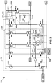
- FIG. 2 shows one topology of one example reduced switch-on slew rate LDO regulator 200 in accordance with one exemplary embodiment that can provide, among other features, limited slew rate switch-on in combination with a stable transition.
- various additional benefits may be a substantial reduction or avoidance of high di/dt, or ringing, or both, on power lines.
- FIG. 2 reduced SSR LDO regulator 200 is shown as an example implementation adapted to, or utilizing portions of the FIG. 1 LDO topology 100.
- This example implementation is for convenience and focus of description on reduced switch-on slew concepts without introducing, and therefore having to fully describe, all structures of an entire LDO regulator topology.
- FIG. 2 example is not intended, though, to limit the scope of any of the exemplary embodiments to structures or practices employing LDO topologies as shown by FIG. 1 .
- reduced switch-on slew rate may be practiced with other differential amplifier topologies, and with various LDO topologies other than the FIG. 1 example 100.
- the reduced SSR LDO regulator 200 comprises a pass gate M9 having a resistance or conductance controlled by controllable slew differential amplifier 204, to apply a voltage drop between the Vdd rail and Vout that maintains Vout, in this example, at Vref. It will be understood that embodiments are not limited to maintaining Vout at Vref. For example, Vout may be made proportional to Vref, by modification readily implemented by persons skilled in the art having view of this disclosure.
- the controllable slew differential amplifier 204 controls the pass gate M9 based on the given reference voltage Vref and a feedback of Vout received, for example, over the previously described feedback path 110.
- the controllable slew differential amplifier 204 feeds, in the FIG. 2 example, a second stage, or intermediate stage buffer (shown but not separately numbered) formed, for example, of the previously described M3, M7, M8 and M10.
- M8 outputs the pass gate control signal Vhg to a pass gate control line 240 that couples to the control gate (input shown, but not separately numbered) of the pass gate M9.
- the controllable slew differential amplifier 204 includes a switchable mode tail current source 250.
- the switchable mode tail current source 250 is configured to be switchable in response to (or in response to a trigger signal that is associated with) a given system on/off or power-up/power-down signal, labeled "ST_ON/OFF.”
- the switchable mode tail current source 250 may be configured to switch, in response to transitions in ST_ON/OFF, between a full-slew, or normal operating mode in which it sources a normal operating bias current, and a reduced-slew mode in which it sources a much smaller, slew-limiting bias current.
- the switchable mode tail current source 250 may include an ON-OFF switchable current source such as switchable full-slew bias current source 252 in parallel with a smaller slew-limiting bias current source 254, which can be always in an ON state.
- the switchable full-slew bias current source 252 may source, in its ON state, a full-slew current, arbitrarily labeled I_ON and, in its OFF state, a zero or approximately zero current.
- the slew-limiting bias current source 254 may be configured to source a much smaller bias current than I_ON, arbitrarily labeled I_SB.
- I_SB may be sufficient to allow the controllable slew differential amplifier 204 to slew over a given interval, but at a much slower rate than would occur if the switchable full-slew bias current source 252 were ON.
- I_ON and I_SB As to the actual magnitude of I_ON and I_SB, it will be appreciated by persons of ordinary skill in the art, from viewing this disclosure, that these magnitudes may be application-specific. Determining I_ON and I_SB for a given application, though, can be readily performed by persons of ordinary skill in the art, for example, by applying conventional bias current selection techniques to the present disclosure. Further detailed description of the actual magnitude of I_ON and I_SB is therefore omitted.
- the reduced SSR LDO regulator 200 may include a slew control feature, described in greater detail at later sections, that provides a timing delay, arbitrarily named in this disclosure as "DLY, before the switchable mode tail current source 250 switches to an ON biasing state after an OFF-to-ON transition of ST_OFF/ON.
- This delayed switching of the switchable mode tail current source 250 can be provided, for example, by generating, in response to an OFF-to-ON transition of ST_OFF/ON, a ramp-up or equivalent time-increasing voltage at the input of a buffer 256.
- the buffer 256 may have its output coupled, for example by a current source control line 257, to a control input (shown but not separately labeled) of the switchable full-slew bias current source 252.
- a signal output of the buffer 256 can be termed a biasing current source control signal (BCS).
- BCS biasing current source control signal
- the buffer 256 switches to generate BCS at an ON level, where "ON" means it switches the switchable full-slew bias current source 252 to an ON state.
- the timing delay DLY may be provided by configuring a circuitry that charges the input to the buffer 256 to ramp-up the voltage to reach the buffer 256 switching threshold at DLY after the OFF-to-PN transition of ST_OFF/ON.
- DLY is implemented by charging current source 260 that, under control of charging switch transistor M20, charges a delay capacitor C2 that is coupled to the input of the buffer 256.
- the DLY value is the charging time duration, starting at an OFF-to-ON transition of ST_OFF/ON and ending when the charge on the delay capacitor C2 reaches an OFF-ON threshold voltage of the buffer 256.
- That OFF-ON threshold voltage of the buffer 256 may be termed "the tail current source mode switch threshold.”
- the DLY value i.e., the charging duration of C2
- the capacitance of C2 may be established by the capacitance of C2, together with the drive capacity of the charging current source 260, and the OFF-ON threshold of the buffer 256.
- selecting DLY can be based, at least in part, on the RC time constant of a discharge path formed by the previously described compensation capacitor C1 and compensation resistor R1 of the Miller feedback compensation network 150, as described in greater detail at later sections.
- the reduced SSR LDO regulator 200 may include a pass gate disabling feature that provides a switching of the pass gate M9 to an OFF state in response to ST_OFF switching to an OFF state.
- the FIG. 2 example reduced SSR LDO regulator 200 includes one example implementation of this feature, utilizing a pass gate disabling switch 270 coupled to the ST_OFF/ON signal by, for example, a pass gate disabling signal line 262, in combination with the compensation capacitor C1. Aspects of the pass gate disabling feature will be further understood from detailed description below of example operations.
- one example operation may begin with an arbitrarily selected event of an ON-to-OFF transition of ST_OFF/ON, which is to a "high" level in this example.
- the ST_OFF/ON transition causes the pass gate disabling switch 270 to move to the operational, i.e., closed, or "LDO_OFF" position.
- the LDO_OFF position functions to short the control gate of the pass gate M9 to the Vdd rail, i.e., shorts the pass gate control line 160 to the Vdd rail.
- the ON-to-OFF transition of ST_OFF/ON over-rides the pass gate control signal Vhg with the Vdd rail voltage. Vdd, in turn, holds the pass gate M9 in an OFF state.
- one terminal of C1 which can be appreciated as being a capacitor of the Miller feedback compensation network 150, is also connected to the Vdd rail through the pass gate disabling switch 270.
- the other terminal of C1, through resistor Rl, is pulled down by the load (not shown) coupled to the Vout port or line. Since the pass gate M9 is OFF, the Vout voltage is approximately 0 volts.
- Input transistor M2 of the controllable slew differential amplifier 204 receives the approximately 0 volts through the feedback path 110 and is therefore OFF.
- the voltage on delay capacitor C2 is discharged through M20 to the given rail Vss, which for this example may be assumed as 0 volts.
- the voltage on delay capacitor C2, being 0 volts causes the switchable full-slew bias current source 252 to switch to its OFF state.
- the FIG. 2 example reduced SSR LDO regulator 200 has a switchable mode tail current source 250 that includes a switchable full-slew bias current source 252 and a slew-limiting bias current source 254. Therefore, while the switchable full-slew bias current source 252 is in its OFF state, the slew-limiting bias current source 254 provides continued flow of a very small bias current I_SB. As also previously described, in an aspect, I_SB is sufficient to allow the controllable slew differential amplifier 204 to slew at a slew-limited or reduced slew rate.
- the reduced SSR LDO regulator 200 slews to Vref at a reduced or slew-limited rate.
- the reduced slew rate is established, at least in part, by the I_SB current, and by the resistance of R1 and the capacitance of C2.
- the reduced slew rate is set such that the voltage on C2 switches the ON-OFF full-slew bias current source ON just after, or substantially concurrent with, Vout reaching Vref.
- the above-described low-rate slewing of the reduced SSR LDO regulator 200 is enabled, and begins, upon the ST_ON/OFF signal opening the pass gate disabling switch 270.
- the opening allows the C1 capacitor to discharge the Vdd volts previously on the pass gate control line 240, through the resistor R1.
- the discharging of the Vhg line allows the controllable slew differential amplifier 204 and the pass gate driver M8 to start slewing the voltage on the pass gate control line 240.
- the slew is limited by the small I_SB current sourced by the slew-limiting bias current source 254, in combination with the compensation cap C1.
- the capacitance of C2 can be configured with the following timing objective: preferably concurrent with or shortly after Vout reaches Vref, the voltage on the delay capacitor C2 reaches the value (e.g., the ON voltage of the buffer 256) that causes a switching ON of the switchable full-slew bias current source 252.
- the biasing current source control signal BCS that is output of the buffer 256 may also be communicated as a regulator state signal "RG_ON, for example, on the regulator state indicator line 258, to a high-level system controller (not shown).
- the above-described operations provide a method for reduced switch-on slew LDO regulating that includes biasing the controllable slew differential amplifier 204, during a normal powered-up operation, with the full-slew bias current I_ON. It will also be understood that above-described operations provide a method for reduced switch-on slew LDO regulating that includes, in response to an ON-to-OFF transition of a system on/off signal ST_ON/OFF, moving the pass gate disabling switch 270 to the disable position. The resulting pulling of the pass gate control line 240 to Vdd over-rides the pass gate control signal Vhg and switches OFF, i.e., disables, the pass gate M9.
- the disabling of the pass gate M9 effectively disables a feedback of the controllable slew differential amplifier 204.
- the ON-to-OFF transition of ST_ON/OFF switches also switches ON the charging switch transistor M20, which pulls the input of the buffer 256 to a level causing it to generate the biasing current source control signal BCS at an OFF level, at which the switchable mode tail current source 250 sources only the slew-limiting bias current I_SB.
- the pass gate disabling switch 270 moves to an operational position, enabling the pass gate M9, allowing C1 to discharge, and enabling the feedback of the controllable slew differential amplifier 204.
- features of a reduced switch-on slew rate LDO regulator include, but are not limited to a reduced rate, or "slow,” turn-on of LDO output from power collapse to Vref, while substantially reducing issues pertaining to in-rush current.
- Another of the various features of reduced switch-on slew rate LDO regulators according to the exemplary embodiments is minimal, if any, added cost relative to a comparable capacity conventional (e.g. FIG. 1 ) LDO regulator known conventional hardware and design overhead.
- a comparable capacity conventional e.g. FIG. 1
- FIG. 2 reduced SSR LDO regulator 200 provides re-use of an existing compensation capacitor, as shown by its re-use of C1 of the Miller feedback compensation network 150, to assist in the reduced slew rate turn-on.
- the FIG. 2 reduced SSR LDO regulator 200 requires only one additional capacitor, the delay capacitor C2.
- the FIG. 2 reduced SSR LDO regulator 200 requires no extra control circuitry to enable or provide the smooth ramp-up. Instead, all "control" can be provided by simply selecting appropriate relative component values, for example capacitances C1, C2, or resistance Rl, or both.
- the above-described FIG. 2 example topology of the switchable mode tail current source 250 is not intended to limit the scope of the embodiments.
- the slew-limiting bias current source 254 may be configured such that, after switching ON in response to an OFF-ON switching of ST_OFF, it stays ON until the reduced SSR LDO regulator 200 slews to an operational state, and then switches OFF.
- FIG. 3 shows a topology 300 with an example of six adaptive bias and compensation LDO regulators, illustrated with abbreviated labels LDO1, LDO2 ... LDO6, connected in parallel and showing parasitic elements (shown but not separately labeled) of the power distribution network that interconnects them.
- LDO1, LDO2 ... LDO6 is according to the FIG. 2 example reduced SSR LDO regulator 200.
- each of the LOD regulators LDO1, LDO2 ... LDO6 has a Vref input (not shown) and that each Vref input is connected to Vref source (not shown).
- At least one Vref source may be shared by two or more of the adaptive bias and compensation LDO regulators LDO1, LDO2 ... LDO6. It will be understood that the FIG. 3 capacitors (shown but not separately labeled) may represent explicitly placed load capacitances as well as parasitic capacitances.
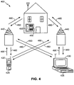
- FIG. 4 illustrates an exemplary wireless communication system 400 in which one or more embodiments of the disclosure may be advantageously employed.
- FIG. 4 shows three remote units 420, 430, and 450 and two base stations 440. It will be recognized that conventional wireless communication systems may have many more remote units and base stations.
- the remote units 420, 430, and 450 include integrated circuit or other semiconductor devices 425, 435 and 455 (including on-chip voltage regulators, as disclosed herein), which are among embodiments of the disclosure as discussed further below.
- FIG. 4 shows forward link signals 480 from the base stations 440 and the remote units 420, 430, and 450 and reverse link signals 490 from the remote units 420, 430, and 450 to the base stations 440.
- the remote unit 420 is shown as a mobile telephone
- the remote unit 430 is shown as a portable computer
- the remote unit 450 is shown as a fixed location remote unit in a wireless local loop system.
- the remote units may be any one or combination of a mobile phone, hand-held personal communication system (PCS) unit, portable data unit such as a personal data assistant (PDA), navigation device (such as GPS enabled devices), set top box, music player, video player, entertainment unit, fixed location data unit such as meter reading equipment, or any other device that stores or retrieves data or computer instructions, or any combination thereof.
- FIG. 4 illustrates remote units according to the teachings of the disclosure, the disclosure is not limited to these exemplary illustrated units. Embodiments of the disclosure may be suitably employed in any device having active integrated circuitry including memory and on-chip circuitry for test and characterization.
- the foregoing disclosed devices and functionalities may be designed and configured into computer files (e.g., RTL, GDSII, GERBER, etc.) stored on computer readable media. Some or all such files may be provided to fabrication handlers who fabricate devices based on such files. Resulting products include semiconductor wafers that are then cut into semiconductor die and packaged into a semiconductor chip. The semiconductor chips can be employed in electronic devices, such as described hereinabove.
- computer files e.g., RTL, GDSII, GERBER, etc.
- Some or all such files may be provided to fabrication handlers who fabricate devices based on such files.
- Resulting products include semiconductor wafers that are then cut into semiconductor die and packaged into a semiconductor chip.
- the semiconductor chips can be employed in electronic devices, such as described hereinabove.
- a software module may reside in RAM memory, flash memory, ROM memory, EPROM memory, EEPROM memory, registers, hard disk, a removable disk, a CD-ROM, or any other form of storage medium known in the art.
- An exemplary storage medium is coupled to the processor such that the processor can read information from, and write information to, the storage medium. In the alternative, the storage medium may be integral to the processor.
- an embodiment of the invention can include a computer readable media embodying a method for implementation. Accordingly, the invention is not limited to illustrated examples and any means for performing the functionality described herein are included in embodiments of the invention.
- the foregoing disclosed devices and functionalities may be designed and configured into computer files (e.g. RTL, GDSII, GERBER, etc.) stored on computer readable media. Some or all such files may be provided to fabrication handlers who fabricate devices based on such files. Resulting products include semiconductor wafers that are then cut into semiconductor die and packaged into a semiconductor chip. The chips are then employed in devices described above.
- computer files e.g. RTL, GDSII, GERBER, etc.
Description
- The technical field of the disclosure relates to voltage regulators and, more particularly, to low dropout (LDO) regulators.
- An LDO regulator is a direct current (DC) linear voltage regulator that can operate with a very low dropout, where "dropout" (also termed "dropout voltage") means the difference between the input voltage (e.g., received power supply rail voltage) and the regulated out voltage. As known in the conventional LDO regulator arts, a low dropout voltage may provide, for example, higher efficiency and concomitant reduction in heat generation, as well as lower minimum operating voltage.
US 2008/061881 discloses a type of voltage regulator.US 2006/0108993 discloses a regulator with low quiescent current. - The following summary is not an extensive overview of all contemplated aspects. Its sole purpose is to present some concepts of one or more aspects in a simplified form as a prelude to the more detailed description that is presented later.
- One example reduced switch-on slew LDO regulator according to one exemplary embodiment can include a pass gate controllably coupling, in response to a pass gate control signal, a voltage rail to a regulator output. In an aspect, the pass gate control signal is generated by a controllable slew differential amplifier, switchable between a slew-limiting state and a full-slew state. Further to the aspect, the controllable slew differential amplifier is configured to receive a feedback from the regulator output, and to generate the pass gate control signal, based on a reference voltage and the feedback, at a full-slew rate in the full-slew state, and at a reduced slew rate in the slew-limiting state.
- One example reduced switch-on slew LDO regulator according to one exemplary embodiment may further include a pass gate disabling circuit configured selectively over-ride the pass gate control signal and switch the pass gate OFF.
- In an aspect, the controllable slew differential amplifier of one example reduced switch-on slew LDO regulator according to one exemplary embodiment may include a switchable tail current source switchable between a slew-limiting bias current and a full-slew bias current. In a related aspect, the controllable slew differential amplifier may be configured to generate the pass gate control signal at the full-slew rate with the full-slew bias current, and at the reduced slew rate with the slew-limiting bias current. In a further aspect, the switchable tail current source may include an ON-OFF switchable full-slew bias current source configured to source the full-slew bias current when ON, in parallel with a reduced slew bias current source configured to source the reduced slew bias current.
- One example reduced switch-on slew LDO regulator according to one exemplary embodiment may further include, in an aspect, a tail current control circuit configured to switch the switchable tail current source to the slew-limiting bias current in response to an ON-to-OFF transition of a system ON-OFF signal (ST_ON/OFF). In a further aspect, the tail current control circuit may be configured to switch the switchable tail current source, at a delay DLY after an OFF-to-ON transition of ST_OFF, from the slew-limiting bias current to the full-slew bias current.
- In a related aspect, the controllable slew differential amplifier may be configured to slew, in response to the OFF-to-ON transition of ST_ON/OFF, from an initial zero voltage to approximately Vref, at a reduced slew rate, in a time duration approximately equal to DLY.
- In another aspect, in one example reduced switch-on slew LDO regulator according to one exemplary embodiment, the tail current control circuit may include a delay capacitor, and a charging circuit configured to charge the delay capacitor, in response to the OFF-to-ON transition of ST_ON/OFF, from a zero voltage to a tail current source switching threshold voltage, in a charging time having a duration approximately equal to DLY.
- In an aspect, one example reduced switch-on slew LDO regulator according to one exemplary embodiment may further include a pass gate control line carrying the pass gate control signal to a control gate of the pass gate. In related aspect, the pass gate disabling circuit may comprise a two-position switch, the two-position switch having a disabling position and an operational position, configured such that the disabling position provides a short of the control gate to a voltage disabling the pass gate, and the operational position does not provide the short of the control gate. In another related aspect, the two-position switch may be configured to be movable, or to move, between the disabling position and the operational position based on an ON-OFF state of ST_OFF/ON.
- One example reduced switch-on slew LDO regulator according to one exemplary embodiment may further include a feedback element that may be coupled to the regulator output and to an input of the differential amplifier to provide the feedback, and a compensation network coupling the pass gate control line to the feedback element. In a further aspect, the compensation network may have a compensation capacitor and a compensation resistor, and the pass gate disabling circuit may be further configured to charge the compensation capacitor when the two-position switch is in the disabling position.
- In another aspect, in one example reduced switch-on slew LDO regulator according to one exemplary embodiment, the pass gate disabling circuit may be further configured to allow the compensation capacitor to discharge the pass gate control line, to a voltage at which the pass gate is operational, in response to switching the two-position switch from the disabling position to the operational position. In a related aspect, a rate of the reduced slew rate may be based, at least in part, on at least one of a capacitance of the compensation capacitor or a resistance of the compensation resistor, or both.
- One example method according to one or more exemplary embodiments may provide reduced switch-on slew low dropout (LDO) regulating with a pass gate controlled by a differential amplifier having differential inputs, and a transistor controlled by one of the differential inputs. Example methods according to various exemplary embodiments may include biasing the transistor with a bias current, the biasing current being a full-slew bias current, and providing to the differential inputs a reference voltage and a feedback of an output of the pass gate. In an aspect, example methods may further provide, in response to an ON-to-OFF transition of a system on/off signal (ST_ON/OFF), disabling the feedback and switching the bias current to a slew-limiting bias current, lower than the full-slew bias current. In a related aspect, example methods may further include, in response to an OFF-to-ON transition of ST_ON/OFF, enabling the feedback to the differential amplifier and, at a time delayed from the OFF-to-ON transition by a reduced slew duration, switching the bias current to the full-slew bias current.
- In one example method according to one exemplary embodiment, the switching the biasing to bias the transistor with the full-slew bias current may include commencing, in response to the OFF-to-ON transition of ST_ON/OFF, a charging of a delay capacitor and, in response to the delay capacitor reaching a given threshold voltage level, performing the switching the biasing to bias the transistor with the full-slew bias current.
- One example reduced switch-on slew LDO regulator according to various exemplary embodiments can include a differential amplifier having difference inputs, an output, and a transistor having a gate coupled to one of the difference inputs, in combination with a pass gate controlled by the output of the differential amplifier. The pass gate may include a pass gate input for coupling to a power rail, and a pass gate output, in further combination with means for receiving a system ON/OFF signal (ST_ON/OFF) and in response to an OFF-to-ON transition of ST_ON/OFF, establishing a feedback from the pass gate output to one of the difference inputs and biasing the transistor with a full-slew bias current, and in response to an ON-to-OFF transition of ST_ON/OFF, disabling the feedback and switching the biasing of the transistor to a slew-limiting bias current.
- The accompanying drawings found in the attachments are presented to aid in the description of embodiments of the invention and are provided solely for illustration of the embodiments and not limitation thereof.
-
FIG. 1 shows a topology for one example LDO regulator unit. -
FIG. 2 shows a topology of one example reduced switch-on slew LDO regulator in accordance with one exemplary embodiment. -
FIG. 3 shows one topology of a power distribution network having a plurality ofFIG. 2 reduced switch-on slew LDO regulator units connected in parallel, exemplary parasitic elements of the interconnecting power distribution network. -
FIG. 4 shows a system diagram of one wireless communication system having, supporting, integrating and/or employing reduced switch-on slew LDO units in accordance with one or more exemplary embodiments. - Aspects of the invention are disclosed in the following description and related drawings directed to specific embodiments of the invention. Alternate embodiments may be devised without departing from the scope of the invention. Additionally, well-known elements of the invention will not be described in detail or will be omitted so as not to obscure the relevant details of the invention.
- The word "exemplary" is used herein to mean "serving as an example, instance, or illustration." Any embodiment described herein as "exemplary" is not necessarily to be construed as preferred or advantageous over other embodiments. Likewise, the term "embodiments of the invention" does not require that all embodiments of the invention include the discussed feature, advantage or mode of operation.
- The terminology used herein is only for the purpose of describing particular examples according to embodiments, and is not intended to be limiting of embodiments of the invention. As used herein, the singular forms "a", "an" and "the" are intended to include the plural forms as well, unless the context clearly indicates otherwise. As used herein the terms "comprises", "comprising,", "includes" and/or "including" specify the presence of stated structural and functional features, steps, operations, elements, and/or components, but do not preclude the presence or addition of one or more other structural and functional feature, steps, operations, elements, components, and/or groups thereof.
- Those of skill in the art will appreciate that information and signals may be represented using any of a variety of different technologies and techniques. For example, data, instructions, commands, information, signals, bits, symbols, and chips that may be referenced throughout the above description may be represented by voltages, currents, electromagnetic waves, magnetic fields or particles, optical fields, electron spins particles, electrospins, or any combination thereof.
- The term "topology" as used herein refers to interconnections of circuit components and, unless stated otherwise, indicates nothing of physical layout of the components or their physical locations relative to one another. Figures described or otherwise identified as showing a topology are no more than a graphical representation of the topology and do not necessarily describe anything regarding physical layout or relative locations of components.
-
FIG. 1 shows a topology for oneexample LDO regulator 100, having adifferential amplifier 104 and a pass gate M9 that provides a controllable resistance (or conductance) coupling between an external power rail Vdd (hereinafter "Vdd rail") and a regulated output voltage Vout terminal. In theFIG. 1 example, the pass gate M9 is a PMOS transistor. Thedifferential amplifier 104 receives as its differential inputs a reference voltage, Vref, and a feedback of Vout (over feedback element or feedback path 110). Thedifferential amplifier 104 generates, based on the difference of Vref and the fed back Vout, a pass gate control signal at Vhg voltage (hereinafter referenced as "pass gate control signal Vhg") that is coupled, by passgate control line 160, to the control gate (shown but not separately numbered) of the pass gate M9. By operation of the feedback, the generated pass gate control signal Vhg drives the resistance of pass gate M9 to a value at which Vout is, in this example, approximately equal to Vref. It will be understood that Vout being approximately equal to Vref is only for purposes of example. For example, a voltage divider (not shown) may be included to generate Vout higher than Vref. - Referring to
FIG. 1 ,differential amplifier 104 is formed of two parallel branches (shown but not separately numbered) extending from the Vdd rail to a common node (shown but not separately numbered). A tailcurrent source 106 sinks abias current 15 from the common node to a reference rail Vss. One of the two branches comprises internal load transistor M5 in series with input transistor M4, the other comprises internal load transistor M6 in series with input transistor M2. The current 15 of the tailcurrent source 106 sets the bias of the input transistors M2 and M4. 15 is fixed. The gate (shown but not separately numbered) of input transistor M4 functions as one of thedifferential amplifier 104 inputs (shown but not separately labeled), and receives Vref. The gate (shown but not separately labeled) of input transistor M2 receives functions as the other of thedifferential amplifier 104 inputs, by receiving Vout through thefeedback path 110. Thedifferential amplifier 104 inputs may be collectively referenced as the "differential inputs" or the "difference inputs." - Referring to
FIG. 1 , transistors M3, M7, M8 and M10 form an intermediate buffer stage (shown but not separately numbered). The drain of M8 drives the passgate control line 160 with the pass gate control signal Vhg. M8 may therefore be considered a drive transistor for the pass gate control signal Vhg. - It will be understood by persons of ordinary skill in the art, having view of this disclosure, that the feedback loop comprises the
differential amplifier 104, the pass control drive transistor M8, the pass gate M9, thefeedback path 110, and the Millerfeedback compensation network 150. The Millerfeedback compensation network 150 may be formed of resistor element R1 and capacitor element C1. The Millerfeedback compensation network 150 produces a dominant pole along with a zero in the feedback response of the feedback loop, which provides stability. The general operation of Miller feedback compensation is known to persons of ordinary skill in the art and, therefore, further detailed description of the operation is omitted except where incidental to other described operation. - A plurality of LDO regulators including, but not limited to the
FIG. 1 example LDO regulator 100, may be used in providing regulated supply voltage within integrated circuit (IC) chips (not shown) having a plurality of circuit blocks (not shown), for example multiple processor cores. Such IC chips may include, in various applications, selective power-up features, for example, selective powering up and powering down individual circuit blocks, or subsets of the circuit blocks. In certain applications, if the powering up of individual circuit blocks (e.g., processor cores) includes simply switching on and off an LDO regulator such as theFIG. 1 example LDO regulator 100, a result may be large in-rush currents. The large in-rush currents, if not mitigated, may result in unwanted incidents of high rate current change, i.e., high di/dt, on the power supply lines. Costs may therefore be incurred, for example, added hardware costs due to a largersized LDO regulator 100 to provide for the large current pulses in such incidents. Another potential effect of high in-rush currents, which in some applications can carry higher costs than high di/dt alone, is ringing on the power supply lines. - One known conventional technique directed to reducing in-rush current, and thus avoiding its above-described effects, is keeping Vref of the
LDO regulator 100 at low or zero voltage until the circuit blocks it supplies are powered up, and then ramping up Vref to its operational value. - However, this known conventional technique can introduce unwanted effects and/or may incur additional costs and, therefore, may be less than preferable. For example, one mechanism that may embody or cause certain unwanted effects is that starting with Vref at a very low (or zero) voltage can render the feedback operation, which is crucial to the
LDO regulator 100, inoperative. -
FIG. 2 shows one topology of one example reduced switch-on slewrate LDO regulator 200 in accordance with one exemplary embodiment that can provide, among other features, limited slew rate switch-on in combination with a stable transition. Among various additional benefits may be a substantial reduction or avoidance of high di/dt, or ringing, or both, on power lines. - For brevity, the term "reduced switch-on slew
rate LDO regulator 200" will alternatively be recited as "reducedSSR LDO regulator 200." It will be understood that "SSR" has no inherent meaning, and imports no meaning from outside this disclosure; it is simply an abbreviation for "switch-on slew rate." - The
FIG. 2 reducedSSR LDO regulator 200 is shown as an example implementation adapted to, or utilizing portions of theFIG. 1 LDO topology 100. This example implementation is for convenience and focus of description on reduced switch-on slew concepts without introducing, and therefore having to fully describe, all structures of an entire LDO regulator topology. It will be understood that theFIG. 2 example is not intended, though, to limit the scope of any of the exemplary embodiments to structures or practices employing LDO topologies as shown byFIG. 1 . For example, it will be readily appreciated by persons of ordinary skill in the art upon reading this disclosure that reduced switch-on slew rate according to one or more exemplary embodiments may be practiced with other differential amplifier topologies, and with various LDO topologies other than theFIG. 1 example 100. - Referring to
FIG. 2 , the reducedSSR LDO regulator 200 comprises a pass gate M9 having a resistance or conductance controlled by controllable slewdifferential amplifier 204, to apply a voltage drop between the Vdd rail and Vout that maintains Vout, in this example, at Vref. It will be understood that embodiments are not limited to maintaining Vout at Vref. For example, Vout may be made proportional to Vref, by modification readily implemented by persons skilled in the art having view of this disclosure. - The controllable slew
differential amplifier 204 controls the pass gate M9 based on the given reference voltage Vref and a feedback of Vout received, for example, over the previously describedfeedback path 110. The controllable slewdifferential amplifier 204 feeds, in theFIG. 2 example, a second stage, or intermediate stage buffer (shown but not separately numbered) formed, for example, of the previously described M3, M7, M8 and M10. In theFIG. 2 example implementation, M8 outputs the pass gate control signal Vhg to a passgate control line 240 that couples to the control gate (input shown, but not separately numbered) of the pass gate M9. - In accordance with one exemplary embodiment, the controllable slew
differential amplifier 204 includes a switchable mode tailcurrent source 250. In an aspect, the switchable mode tailcurrent source 250 is configured to be switchable in response to (or in response to a trigger signal that is associated with) a given system on/off or power-up/power-down signal, labeled "ST_ON/OFF." In an aspect, the switchable mode tailcurrent source 250 may be configured to switch, in response to transitions in ST_ON/OFF, between a full-slew, or normal operating mode in which it sources a normal operating bias current, and a reduced-slew mode in which it sources a much smaller, slew-limiting bias current. - Referring to
FIG. 2 , in an aspect the switchable mode tailcurrent source 250 may include an ON-OFF switchable current source such as switchable full-slew biascurrent source 252 in parallel with a smaller slew-limiting biascurrent source 254, which can be always in an ON state. Further to this aspect, the switchable full-slew biascurrent source 252 may source, in its ON state, a full-slew current, arbitrarily labeled I_ON and, in its OFF state, a zero or approximately zero current. The slew-limiting biascurrent source 254 may be configured to source a much smaller bias current than I_ON, arbitrarily labeled I_SB. The magnitude of I_SB, in an aspect, may be sufficient to allow the controllable slewdifferential amplifier 204 to slew over a given interval, but at a much slower rate than would occur if the switchable full-slew biascurrent source 252 were ON. - As to the actual magnitude of I_ON and I_SB, it will be appreciated by persons of ordinary skill in the art, from viewing this disclosure, that these magnitudes may be application-specific. Determining I_ON and I_SB for a given application, though, can be readily performed by persons of ordinary skill in the art, for example, by applying conventional bias current selection techniques to the present disclosure. Further detailed description of the actual magnitude of I_ON and I_SB is therefore omitted.
- With respect to topologies and technologies for implementing the switchable full-slew bias
current source 252, and the slew-limiting biascurrent source 254, in an aspect these may be according to general known conventional techniques for current sources and switchable current sources. Further detailed description is therefore omitted. - In an aspect, the reduced
SSR LDO regulator 200 may include a slew control feature, described in greater detail at later sections, that provides a timing delay, arbitrarily named in this disclosure as "DLY, before the switchable mode tailcurrent source 250 switches to an ON biasing state after an OFF-to-ON transition of ST_OFF/ON. This delayed switching of the switchable mode tailcurrent source 250 can be provided, for example, by generating, in response to an OFF-to-ON transition of ST_OFF/ON, a ramp-up or equivalent time-increasing voltage at the input of abuffer 256. Thebuffer 256 may have its output coupled, for example by a currentsource control line 257, to a control input (shown but not separately labeled) of the switchable full-slew biascurrent source 252. In a related aspect, a signal output of thebuffer 256 can be termed a biasing current source control signal (BCS). In a further aspect, when the input voltage of thebuffer 256 reaches what may be termed an OFF-to-ON logical switching threshold, thebuffer 256 switches to generate BCS at an ON level, where "ON" means it switches the switchable full-slew biascurrent source 252 to an ON state. - In one aspect, the timing delay DLY may be provided by configuring a circuitry that charges the input to the
buffer 256 to ramp-up the voltage to reach thebuffer 256 switching threshold at DLY after the OFF-to-PN transition of ST_OFF/ON. For example, in theFIG. 2 reducedSSR LDO regulator 200, DLY is implemented by chargingcurrent source 260 that, under control of charging switch transistor M20, charges a delay capacitor C2 that is coupled to the input of thebuffer 256. The DLY value is the charging time duration, starting at an OFF-to-ON transition of ST_OFF/ON and ending when the charge on the delay capacitor C2 reaches an OFF-ON threshold voltage of thebuffer 256. That OFF-ON threshold voltage of thebuffer 256 may be termed "the tail current source mode switch threshold." In an aspect, the DLY value, i.e., the charging duration of C2, may be established by the capacitance of C2, together with the drive capacity of the chargingcurrent source 260, and the OFF-ON threshold of thebuffer 256. In an aspect, selecting DLY can be based, at least in part, on the RC time constant of a discharge path formed by the previously described compensation capacitor C1 and compensation resistor R1 of the Millerfeedback compensation network 150, as described in greater detail at later sections. - Referring to
FIG. 2 , in an aspect, the reducedSSR LDO regulator 200 may include a pass gate disabling feature that provides a switching of the pass gate M9 to an OFF state in response to ST_OFF switching to an OFF state. TheFIG. 2 example reducedSSR LDO regulator 200 includes one example implementation of this feature, utilizing a passgate disabling switch 270 coupled to the ST_OFF/ON signal by, for example, a pass gate disablingsignal line 262, in combination with the compensation capacitor C1. Aspects of the pass gate disabling feature will be further understood from detailed description below of example operations. - Example operations demonstrating, on the
FIG. 2 reducedSSR LDO regulator 200, concepts according to various embodiments will now be described. As a preliminary matter, it will be understood that in describing transitions of ST_OFF/ON, the phrases "ON-to-OFF transition (or transitioning)" are used, for brevity, in place of "transition (or transitioning) from an ON state to an OFF state." Likewise, the phrases "OFF-to-ON transition (or transitioning)" are used in place of "transition (or transitioning) from an OFF state to an ON state." - Referring still to
FIG. 2 , one example operation may begin with an arbitrarily selected event of an ON-to-OFF transition of ST_OFF/ON, which is to a "high" level in this example. The ST_OFF/ON transition causes the passgate disabling switch 270 to move to the operational, i.e., closed, or "LDO_OFF" position. The LDO_OFF position functions to short the control gate of the pass gate M9 to the Vdd rail, i.e., shorts the passgate control line 160 to the Vdd rail. In an aspect, the ON-to-OFF transition of ST_OFF/ON over-rides the pass gate control signal Vhg with the Vdd rail voltage. Vdd, in turn, holds the pass gate M9 in an OFF state. Referring toFIG. 2 , it is seen that one terminal of C1, which can be appreciated as being a capacitor of the Millerfeedback compensation network 150, is also connected to the Vdd rail through the passgate disabling switch 270. The other terminal of C1, through resistor Rl, is pulled down by the load (not shown) coupled to the Vout port or line. Since the pass gate M9 is OFF, the Vout voltage is approximately 0 volts. Input transistor M2 of the controllable slewdifferential amplifier 204 receives the approximately 0 volts through thefeedback path 110 and is therefore OFF. At the same time, or at substantially the same time, the voltage on delay capacitor C2 is discharged through M20 to the given rail Vss, which for this example may be assumed as 0 volts. The voltage on delay capacitor C2, being 0 volts, causes the switchable full-slew biascurrent source 252 to switch to its OFF state. - As previously described, the
FIG. 2 example reducedSSR LDO regulator 200 has a switchable mode tailcurrent source 250 that includes a switchable full-slew biascurrent source 252 and a slew-limiting biascurrent source 254. Therefore, while the switchable full-slew biascurrent source 252 is in its OFF state, the slew-limiting biascurrent source 254 provides continued flow of a very small bias current I_SB. As also previously described, in an aspect, I_SB is sufficient to allow the controllable slewdifferential amplifier 204 to slew at a slew-limited or reduced slew rate. When an OFF-to-ON transition of ST_ON/OFF occurs, (i.e., when ST_ON/OFF transitions from high to low, using the example polarities), there are two resulting actions. One is the passgate disabling switch 270 moves to the LDO_ON position, i.e., the passgate disabling switch 270 opens. The other is the ST_ON/OFF trigger switch M20 switches OFF, in turn allowing thecurrent source 260 to charge the delay capacitor C2. When the delay capacitor C2 reaches the OFF-ON threshold voltage of thebuffer 256, thebuffer 256 outputs the biasing current source control signal BCS at the ON level. The switchable full-slew biascurrent source 252 switches ON. - In an aspect, prior to the delay capacitor C2 reaching the OFF-ON threshold of the
buffer 256, the reducedSSR LDO regulator 200 slews to Vref at a reduced or slew-limited rate. The reduced slew rate is established, at least in part, by the I_SB current, and by the resistance of R1 and the capacitance of C2. In an aspect, the reduced slew rate is set such that the voltage on C2 switches the ON-OFF full-slew bias current source ON just after, or substantially concurrent with, Vout reaching Vref. - It will be understood that the above-described low-rate slewing of the reduced
SSR LDO regulator 200 is enabled, and begins, upon the ST_ON/OFF signal opening the passgate disabling switch 270. The opening allows the C1 capacitor to discharge the Vdd volts previously on the passgate control line 240, through the resistor R1. The discharging of the Vhg line, in turn, allows the controllable slewdifferential amplifier 204 and the pass gate driver M8 to start slewing the voltage on the passgate control line 240. The slew, however, is limited by the small I_SB current sourced by the slew-limiting biascurrent source 254, in combination with the compensation cap C1. - As the voltage on the Vhg is slewing, at a reduced rate limited by I_SB of the slew-limiting bias
current source 254, as well as the capacitance of C1 and the resistance of R1, the voltage on the delay capacitor C2 is also increasing, as described above. In an aspect, the capacitance of C2, the capacitance of C1 and resistance of R1 can be configured with the following timing objective: preferably concurrent with or shortly after Vout reaches Vref, the voltage on the delay capacitor C2 reaches the value (e.g., the ON voltage of the buffer 256) that causes a switching ON of the switchable full-slew biascurrent source 252. Persons of ordinary skill in the art, having view of the present disclosure, can readily configure the resistance of R1, and the respective capacitances of C1 and C2 such that theFIG. 2 reducedSSR LDO regulator 200 or its equivalent implementations, meet this timing objective, without undue experimentation. For example, without limitation, such persons can implement capacitors C1 and C2 using the same process type, or derivecurrent sources - Referring to
FIG. 2 , in an aspect, the biasing current source control signal BCS that is output of thebuffer 256 may also be communicated as a regulator state signal "RG_ON, for example, on the regulatorstate indicator line 258, to a high-level system controller (not shown). - It will be understood that the above-described operations provide a method for reduced switch-on slew LDO regulating that includes biasing the controllable slew
differential amplifier 204, during a normal powered-up operation, with the full-slew bias current I_ON. It will also be understood that above-described operations provide a method for reduced switch-on slew LDO regulating that includes, in response to an ON-to-OFF transition of a system on/off signal ST_ON/OFF, moving the passgate disabling switch 270 to the disable position. The resulting pulling of the passgate control line 240 to Vdd over-rides the pass gate control signal Vhg and switches OFF, i.e., disables, the pass gate M9. The disabling of the pass gate M9 effectively disables a feedback of the controllable slewdifferential amplifier 204. The ON-to-OFF transition of ST_ON/OFF, switches also switches ON the charging switch transistor M20, which pulls the input of thebuffer 256 to a level causing it to generate the biasing current source control signal BCS at an OFF level, at which the switchable mode tailcurrent source 250 sources only the slew-limiting bias current I_SB. Then, in response to an OFF-to-ON transition of ST_ON/OFF, the passgate disabling switch 270 moves to an operational position, enabling the pass gate M9, allowing C1 to discharge, and enabling the feedback of the controllable slewdifferential amplifier 204. These operations, in turn, allow the controllable slewdifferential amplifier 204 to slew toward Vref. But the delay capacitor C2 causes a delay, DLY, in the switchable mode tailcurrent source 250 switching to the full-slew bias current I_ON. Until expiration of the delay DLY after the OFF-to-ON transition of ST_ON/OFF, the controllable slewdifferential amplifier 204 slews at a reduced slew rate imposed by the slew-limiting bias current I_SB. Upon expiration of the delay DLT, the delay capacitor C2 reaches the switching threshold of thebuffer 256, causing it to output the biasing current control signal BCS to the switchable mode tailcurrent source 250 at the ON level. The resulting I_ON biases the controllable slewdifferential amplifier 204 to a full-slew operation. - As readily appreciated by persons of skill from the present disclosure, features of a reduced switch-on slew rate LDO regulator according to the exemplary embodiments include, but are not limited to a reduced rate, or "slow," turn-on of LDO output from power collapse to Vref, while substantially reducing issues pertaining to in-rush current. Another of the various features of reduced switch-on slew rate LDO regulators according to the exemplary embodiments is minimal, if any, added cost relative to a comparable capacity conventional (e.g.
FIG. 1 ) LDO regulator known conventional hardware and design overhead. For example, theFIG. 2 reducedSSR LDO regulator 200 provides re-use of an existing compensation capacitor, as shown by its re-use of C1 of the Millerfeedback compensation network 150, to assist in the reduced slew rate turn-on. As another example, theFIG. 2 reducedSSR LDO regulator 200 requires only one additional capacitor, the delay capacitor C2. As still another example, theFIG. 2 reducedSSR LDO regulator 200 requires no extra control circuitry to enable or provide the smooth ramp-up. Instead, all "control" can be provided by simply selecting appropriate relative component values, for example capacitances C1, C2, or resistance Rl, or both. - It will be understood that the above-described
FIG. 2 example topology of the switchable mode tailcurrent source 250 is not intended to limit the scope of the embodiments. For example, in one alternative aspect the slew-limiting biascurrent source 254 may be configured such that, after switching ON in response to an OFF-ON switching of ST_OFF, it stays ON until the reducedSSR LDO regulator 200 slews to an operational state, and then switches OFF. -
FIG. 3 shows atopology 300 with an example of six adaptive bias and compensation LDO regulators, illustrated with abbreviated labels LDO1, LDO2 ... LDO6, connected in parallel and showing parasitic elements (shown but not separately labeled) of the power distribution network that interconnects them. It may be assumed that each of adaptive bias and compensation LDO regulators LDO1, LDO2 ... LDO6 is according to theFIG. 2 example reducedSSR LDO regulator 200. It may be assumed that each of the LOD regulators LDO1, LDO2 ... LDO6 has a Vref input (not shown) and that each Vref input is connected to Vref source (not shown). In an aspect, at least one Vref source (not shown) may be shared by two or more of the adaptive bias and compensation LDO regulators LDO1, LDO2 ... LDO6. It will be understood that theFIG. 3 capacitors (shown but not separately labeled) may represent explicitly placed load capacitances as well as parasitic capacitances. -
FIG. 4 illustrates an exemplarywireless communication system 400 in which one or more embodiments of the disclosure may be advantageously employed. For purposes of illustration,FIG. 4 shows threeremote units base stations 440. It will be recognized that conventional wireless communication systems may have many more remote units and base stations. Theremote units other semiconductor devices FIG. 4 shows forward link signals 480 from thebase stations 440 and theremote units remote units base stations 440. - In
FIG. 4 , theremote unit 420 is shown as a mobile telephone, theremote unit 430 is shown as a portable computer, and theremote unit 450 is shown as a fixed location remote unit in a wireless local loop system. For example, the remote units may be any one or combination of a mobile phone, hand-held personal communication system (PCS) unit, portable data unit such as a personal data assistant (PDA), navigation device (such as GPS enabled devices), set top box, music player, video player, entertainment unit, fixed location data unit such as meter reading equipment, or any other device that stores or retrieves data or computer instructions, or any combination thereof. AlthoughFIG. 4 illustrates remote units according to the teachings of the disclosure, the disclosure is not limited to these exemplary illustrated units. Embodiments of the disclosure may be suitably employed in any device having active integrated circuitry including memory and on-chip circuitry for test and characterization. - The foregoing disclosed devices and functionalities (such as the devices of
FIGS. 2 ,3 or4 or any combination thereof) may be designed and configured into computer files (e.g., RTL, GDSII, GERBER, etc.) stored on computer readable media. Some or all such files may be provided to fabrication handlers who fabricate devices based on such files. Resulting products include semiconductor wafers that are then cut into semiconductor die and packaged into a semiconductor chip. The semiconductor chips can be employed in electronic devices, such as described hereinabove. - The methods, sequences and/or algorithms described in connection with the embodiments disclosed herein may be embodied directly in hardware, in a software module executed by a processor, or in a combination of the two. A software module may reside in RAM memory, flash memory, ROM memory, EPROM memory, EEPROM memory, registers, hard disk, a removable disk, a CD-ROM, or any other form of storage medium known in the art. An exemplary storage medium is coupled to the processor such that the processor can read information from, and write information to, the storage medium. In the alternative, the storage medium may be integral to the processor.
- Accordingly, an embodiment of the invention can include a computer readable media embodying a method for implementation. Accordingly, the invention is not limited to illustrated examples and any means for performing the functionality described herein are included in embodiments of the invention.
- The foregoing disclosed devices and functionalities may be designed and configured into computer files (e.g. RTL, GDSII, GERBER, etc.) stored on computer readable media. Some or all such files may be provided to fabrication handlers who fabricate devices based on such files. Resulting products include semiconductor wafers that are then cut into semiconductor die and packaged into a semiconductor chip. The chips are then employed in devices described above.
- While the foregoing disclosure shows illustrative embodiments of the invention, it should be noted that various changes and modifications could be made herein without departing from the scope of the invention as defined by the appended claims. The functions, steps and/or actions of the method claims in accordance with the embodiments of the invention described herein need not be performed in any particular order. Furthermore, although elements of the invention may be described or claimed in the singular, the plural is contemplated unless limitation to the singular is explicitly stated.
Claims (9)
- A reduced switch-on slew low dropout, LDO, regulator comprising:a pass gate (M9) controllably coupling, in response to a pass gate control signal, Vhg, a voltage rail, Vdd, to a regulator output, Vout;a controllable slew differential amplifier (204), switchable between a slew-limiting state and a full-slew state, configured to receive a feedback from the regulator output, and to generate the pass gate control signal, based on a reference voltage, Vref, and the feedback, at a full-slew rate in the full-slew state, and at a reduced slew rate in the slew-limiting state;a pass gate disabling circuit (270) configured to selectively over-ride the pass gate control signal and switch the pass gate OFF;wherein the controllable slew differential amplifier includes a switchable tail current source (250) that is switchable between sourcing a slew-limiting bias current, I_SB, and sourcing a full-slew bias current, I_ON, and is configured to generate the pass gate control signal at the full-slew rate with the full-slew bias current, and at the reduced slew rate with the slew-limiting bias current; and characterized by:
a tail current control circuit (256, 260, M20, C2) configured to switch (M20, 256) the switchable tail current source to the slew-limiting bias current in response to an ON-to-OFF transition of a system ON-OFF signal, ST_ON/OFF and, at a delay DLY after an OFF-to-ON transition of ST_OFF, to switch the switchable tail current source from the slew-limiting bias current to the full-slew bias current. - The reduced switch-on slew LDO regulator of claim 1, wherein the switchable tail current source includes a switchable full-slew bias current source (252) configured to source the full-slew bias current, I_ON, when ON, in parallel with a slew-limiting bias current source (254) configured to source the slew-limiting bias current, I_SB.
- The reduced switch-on slew LDO regulator of claim 1, wherein the controllable slew differential amplifier is configured to slew, in response to the OFF-to-ON transition of ST_ON/OFF, from an initial zero voltage to approximately Vref, at a slew rate slewing from the initial zero voltage to approximately Vref in a time duration approximately equal to DLY.
- The reduced switch-on slew LDO regulator of claim 3, wherein the tail current control circuit includes a delay capacitor (C2), and a charging circuit configured to charge the delay capacitor, in response to the OFF-to-ON transition of ST_ON/OFF, from a zero voltage to a tail current source mode switch threshold, in a charging time having a duration approximately equal to DLY.
- The reduced switch-on slew LDO regulator of claim 4, wherein the charging circuit includes a trigger switch coupled to a charging current source.
- The reduced switch-on slew LDO regulator of claim 1, further comprising: a pass gate control line (257) carrying the pass gate control signal to a control gate of the pass gate, wherein the pass gate disabling circuit comprises a two-position switch (270), the two-position switch having a disabling position and an operational position, wherein the disabling position provides a short of the control gate to a voltage, Vdd, disabling the pass gate, and the operational position does not provide the short of the control gate, wherein the two-position switch is configured to switch between the disabling position and the operational position based on an ON-OFF state of ST_OFF/ON.
- A method for reduced switch-on slew low dropout, LDO, regulating with a pass gate (M9) controlled by a differential amplifier (204) having differential inputs, and a transistor (M2, M4) controlled by one of the differential inputs, comprising:biasing the transistor with a bias current, I_ON, the bias current being a full-slew bias current;providing to the differential inputs a reference voltage, Vref, and a feedback (110) of an output, Vout, of the pass gate;in response to an ON-to-OFF transition of a system on/off signal (ST_ON/OFF), disabling the feedback and switching (M20, 256) the bias current to a slew-limiting bias current, I_SB, lower than a full-slew bias current;in response to an OFF-to-ON transition of ST_ON/OFF, enabling the feedback to the differential amplifier; andat a time delayed from said OFF-to-ON transition by a reduced slew duration, switching the bias current to biasing to the full-slew bias current, the time delay implemented by current source (260) charging a delay capacitor (C2), under control of charging switch transistor (M20);wherein biasing the transistor with the full-slew bias current includes commencing, in response to said OFF-to-ON transition, a charging of a delay capacitor (C1) and, in response to the delay capacitor reaching a given threshold voltage level, performing the switching the biasing to bias the transistor with the full-slew bias current.
- A method for reduced switch-on slew low dropout, LDO, regulating with a pass gate (M9) controlled by a differential amplifier (204) having differential inputs, and a transistor (M2, M4) controlled by one of the differential inputs, comprising:biasing the transistor with a bias current, I_ON, the bias current being a full-slew bias current;providing to the differential inputs a reference voltage, Vref, and a feedback (110) of an output, Vout, of the pass gate;in response to an ON-to-OFF transition of a system on/off signal, ST_ON/OFF, disabling the feedback and switching (M20, 256) the bias current to a slew-limiting bias current, I_SB, lower than a full-slew bias current;in response to an OFF-to-ON transition of ST_ON/OFF, enabling the feedback to the differential amplifier; andat a time delayed from said OFF-to-ON transition by a reduced slew duration, switching the bias current to biasing to the full-slew bias current, the time delay implemented by current source (260) charging a delay capacitor (C2), under control of charging switch transistor (M20);wherein biasing the transistor with the full-slew bias current comprises:generating, in response to the ON state of ST_ON/OFF, a biasing current source control signal at an ON level, andcontrolling a current source (252) coupled to the transistor based on the biasing current source control signal at the ON level.
- An apparatus comprising means for performing a method in accordance with any of claims 7 and 8.
Priority Applications (1)
| Application Number | Priority Date | Filing Date | Title |
|---|---|---|---|
| EP18190338.6A EP3422135B1 (en) | 2012-11-06 | 2013-11-05 | Method and apparatus reduced switch-on rate low dropout regulator (ldo) bias and compensation |
Applications Claiming Priority (3)
| Application Number | Priority Date | Filing Date | Title |
|---|---|---|---|
| US201261722876P | 2012-11-06 | 2012-11-06 | |
| US13/788,115 US9235225B2 (en) | 2012-11-06 | 2013-03-07 | Method and apparatus reduced switch-on rate low dropout regulator (LDO) bias and compensation |
| PCT/US2013/068522 WO2014074520A2 (en) | 2012-11-06 | 2013-11-05 | Method and apparatus reduced switch-on rate low dropout regulator (ldo) bias and compensation |
Related Child Applications (2)
| Application Number | Title | Priority Date | Filing Date |
|---|---|---|---|
| EP18190338.6A Division EP3422135B1 (en) | 2012-11-06 | 2013-11-05 | Method and apparatus reduced switch-on rate low dropout regulator (ldo) bias and compensation |
| EP18190338.6A Division-Into EP3422135B1 (en) | 2012-11-06 | 2013-11-05 | Method and apparatus reduced switch-on rate low dropout regulator (ldo) bias and compensation |
Publications (2)
| Publication Number | Publication Date |
|---|---|
| EP2917800A2 EP2917800A2 (en) | 2015-09-16 |
| EP2917800B1 true EP2917800B1 (en) | 2018-09-26 |
Family
ID=50621759
Family Applications (2)
| Application Number | Title | Priority Date | Filing Date |
|---|---|---|---|
| EP13795635.5A Active EP2917800B1 (en) | 2012-11-06 | 2013-11-05 | Method and apparatus reduced switch-on rate low dropout regulator (ldo) bias and compensation |
| EP18190338.6A Active EP3422135B1 (en) | 2012-11-06 | 2013-11-05 | Method and apparatus reduced switch-on rate low dropout regulator (ldo) bias and compensation |
Family Applications After (1)
| Application Number | Title | Priority Date | Filing Date |
|---|---|---|---|
| EP18190338.6A Active EP3422135B1 (en) | 2012-11-06 | 2013-11-05 | Method and apparatus reduced switch-on rate low dropout regulator (ldo) bias and compensation |
Country Status (7)
| Country | Link |
|---|---|
| US (1) | US9235225B2 (en) |
| EP (2) | EP2917800B1 (en) |
| JP (2) | JP6465804B2 (en) |
| CN (1) | CN104756032B (en) |
| ES (2) | ES2701998T3 (en) |
| HU (1) | HUE040259T2 (en) |
| WO (1) | WO2014074520A2 (en) |
Families Citing this family (16)
| Publication number | Priority date | Publication date | Assignee | Title |
|---|---|---|---|---|
| US9122293B2 (en) | 2012-10-31 | 2015-09-01 | Qualcomm Incorporated | Method and apparatus for LDO and distributed LDO transient response accelerator |
| US9170590B2 (en) | 2012-10-31 | 2015-10-27 | Qualcomm Incorporated | Method and apparatus for load adaptive LDO bias and compensation |
| US8981745B2 (en) | 2012-11-18 | 2015-03-17 | Qualcomm Incorporated | Method and apparatus for bypass mode low dropout (LDO) regulator |
| US11095216B2 (en) | 2014-05-30 | 2021-08-17 | Qualcomm Incorporated | On-chip dual-supply multi-mode CMOS regulators |
| CN104063003B (en) * | 2014-06-27 | 2015-10-21 | 合肥工业大学 | A kind of low-power consumption of integrated slew rate enhancing circuit is without the outer electric capacity LDO of sheet |
| TWI534584B (en) * | 2015-05-20 | 2016-05-21 | 晶宏半導體股份有限公司 | Self discharge regulator device for display |
| KR102409919B1 (en) * | 2015-09-02 | 2022-06-16 | 삼성전자주식회사 | Regulator circuit and power system including the same |
| US9933800B1 (en) | 2016-09-30 | 2018-04-03 | Synaptics Incorporated | Frequency compensation for linear regulators |
| EP3672052A4 (en) | 2017-08-16 | 2020-08-19 | Huawei Technologies Co., Ltd. | Voltage regulation circuit |
| US10013005B1 (en) * | 2017-08-31 | 2018-07-03 | Xilinx, Inc. | Low voltage regulator |
| JP6592126B2 (en) | 2018-02-09 | 2019-10-16 | 華邦電子股▲ふん▼有限公司Winbond Electronics Corp. | Bit line power supply device |
| KR20220010125A (en) * | 2020-07-17 | 2022-01-25 | 에스케이하이닉스 주식회사 | Amplifier and voltage generation circuit including the amplifier |
| CN112034924B (en) * | 2020-08-10 | 2023-02-24 | 唯捷创芯(天津)电子技术股份有限公司 | Self-adaptive fast response LDO (low dropout regulator) circuit and chip thereof |
| JP7391791B2 (en) * | 2020-08-12 | 2023-12-05 | 株式会社東芝 | constant voltage circuit |
| CN112462834B (en) * | 2020-10-27 | 2022-05-13 | 北京智芯微电子科技有限公司 | Current bias circuit for fast wake-up chip |
| KR102609484B1 (en) * | 2021-11-22 | 2023-12-01 | 고려대학교 산학협력단 | Hybrid ldo regulator using operational trans-conductance amplifier |
Citations (1)
| Publication number | Priority date | Publication date | Assignee | Title |
|---|---|---|---|---|
| US20060108993A1 (en) * | 2004-11-19 | 2006-05-25 | Sunplus Technology Co., Ltd. | Voltage regulator circuit with a low quiescent current |
Family Cites Families (58)
| Publication number | Priority date | Publication date | Assignee | Title |
|---|---|---|---|---|
| US4656647A (en) | 1985-05-17 | 1987-04-07 | William Hotine | Pulsed bi-phase digital modulator system |
| JP2785732B2 (en) | 1995-02-08 | 1998-08-13 | 日本電気株式会社 | Power supply step-down circuit |
| US6046577A (en) | 1997-01-02 | 2000-04-04 | Texas Instruments Incorporated | Low-dropout voltage regulator incorporating a current efficient transient response boost circuit |
| US5982226A (en) | 1997-04-07 | 1999-11-09 | Texas Instruments Incorporated | Optimized frequency shaping circuit topologies for LDOs |
| JPH11231954A (en) * | 1998-02-16 | 1999-08-27 | Mitsubishi Electric Corp | Internal power supply voltage generation circuit |
| US6031417A (en) | 1998-04-01 | 2000-02-29 | Rockwell International | Differential amplifier for multiple supply voltages and biasing device therefore |
| US6188211B1 (en) | 1998-05-13 | 2001-02-13 | Texas Instruments Incorporated | Current-efficient low-drop-out voltage regulator with improved load regulation and frequency response |
| JP4472069B2 (en) | 1999-11-10 | 2010-06-02 | オリンパス株式会社 | Medical capsule endoscope |
| US6188212B1 (en) | 2000-04-28 | 2001-02-13 | Burr-Brown Corporation | Low dropout voltage regulator circuit including gate offset servo circuit powered by charge pump |
| US6373233B2 (en) * | 2000-07-17 | 2002-04-16 | Philips Electronics No. America Corp. | Low-dropout voltage regulator with improved stability for all capacitive loads |
| US6246221B1 (en) | 2000-09-20 | 2001-06-12 | Texas Instruments Incorporated | PMOS low drop-out voltage regulator using non-inverting variable gain stage |
| US6333623B1 (en) | 2000-10-30 | 2001-12-25 | Texas Instruments Incorporated | Complementary follower output stage circuitry and method for low dropout voltage regulator |
| US6522111B2 (en) | 2001-01-26 | 2003-02-18 | Linfinity Microelectronics | Linear voltage regulator using adaptive biasing |
| US6518737B1 (en) | 2001-09-28 | 2003-02-11 | Catalyst Semiconductor, Inc. | Low dropout voltage regulator with non-miller frequency compensation |
| US6703815B2 (en) | 2002-05-20 | 2004-03-09 | Texas Instruments Incorporated | Low drop-out regulator having current feedback amplifier and composite feedback loop |
| US6617833B1 (en) * | 2002-04-01 | 2003-09-09 | Texas Instruments Incorporated | Self-initialized soft start for Miller compensated regulators |
| KR100528789B1 (en) * | 2003-08-01 | 2005-11-15 | 주식회사 하이닉스반도체 | Clock enable buffer to enter self refresh mode |
| US6879142B2 (en) | 2003-08-20 | 2005-04-12 | Broadcom Corporation | Power management unit for use in portable applications |
| JP2005205072A (en) | 2004-01-26 | 2005-08-04 | Olympus Corp | Capsule type medical device |
| US7368896B2 (en) | 2004-03-29 | 2008-05-06 | Ricoh Company, Ltd. | Voltage regulator with plural error amplifiers |
| US7091710B2 (en) | 2004-05-03 | 2006-08-15 | System General Corp. | Low dropout voltage regulator providing adaptive compensation |
| EP1635239A1 (en) | 2004-09-14 | 2006-03-15 | Dialog Semiconductor GmbH | Adaptive biasing concept for current mode voltage regulators |
| US7215103B1 (en) | 2004-12-22 | 2007-05-08 | National Semiconductor Corporation | Power conservation by reducing quiescent current in low power and standby modes |
| JP2006230680A (en) | 2005-02-24 | 2006-09-07 | Pentax Corp | Capsule type medical device |
| JP4523473B2 (en) | 2005-04-04 | 2010-08-11 | 株式会社リコー | Constant voltage circuit |
| DE102005015522A1 (en) | 2005-04-04 | 2006-10-05 | Karl Storz Gmbh & Co. Kg | Intracorporal probe for human or animal body, has image acquisition unit designed for optical admission of area outside probe, and movably held within housing in order to change movement of admission area |
| JP4695432B2 (en) | 2005-04-12 | 2011-06-08 | オリンパスメディカルシステムズ株式会社 | In-subject introduction apparatus, in-subject information display apparatus, and in-subject information acquisition system |
| DE102005039114B4 (en) | 2005-08-18 | 2007-06-28 | Texas Instruments Deutschland Gmbh | Voltage regulator with a low voltage drop |
| FR2896051B1 (en) | 2006-01-09 | 2008-04-18 | St Microelectronics Sa | SERIES VOLTAGE VOLTAGE REGULATOR WITH LOW VOLTAGE INSERTION |
| JP2007280025A (en) | 2006-04-06 | 2007-10-25 | Seiko Epson Corp | Power supply device |
| EP1865397B1 (en) | 2006-06-05 | 2012-11-21 | St Microelectronics S.A. | Low drop-out voltage regulator |
| JP4653046B2 (en) * | 2006-09-08 | 2011-03-16 | 株式会社リコー | Differential amplifier circuit, voltage regulator using the differential amplifier circuit, and differential amplifier circuit operation control method |
| JP4914738B2 (en) * | 2007-02-17 | 2012-04-11 | セイコーインスツル株式会社 | Voltage regulator |
| US7728569B1 (en) | 2007-04-10 | 2010-06-01 | Altera Corporation | Voltage regulator circuitry with adaptive compensation |
| CN100495281C (en) * | 2007-09-07 | 2009-06-03 | 北京时代民芯科技有限公司 | Low-voltage-difference voltage-stablizer |
| JP4937865B2 (en) | 2007-09-11 | 2012-05-23 | 株式会社リコー | Constant voltage circuit |
| KR100924293B1 (en) | 2007-09-14 | 2009-10-30 | 한국과학기술원 | Low voltage drop out regulator |
| US7804415B2 (en) | 2007-09-14 | 2010-09-28 | Astec International Limited | Health monitoring for power converter components |
| US8072196B1 (en) | 2008-01-15 | 2011-12-06 | National Semiconductor Corporation | System and method for providing a dynamically configured low drop out regulator with zero quiescent current and fast transient response |
| JP5035987B2 (en) | 2008-01-28 | 2012-09-26 | 富士フイルム株式会社 | Capsule endoscope and operation control method of capsule endoscope |
| US7768351B2 (en) | 2008-06-25 | 2010-08-03 | Texas Instruments Incorporated | Variable gain current input amplifier and method |
| JP5112208B2 (en) * | 2008-07-18 | 2013-01-09 | ルネサスエレクトロニクス株式会社 | Regulator and semiconductor device |
| US8080983B2 (en) | 2008-11-03 | 2011-12-20 | Microchip Technology Incorporated | Low drop out (LDO) bypass voltage regulator |
| US8305056B2 (en) * | 2008-12-09 | 2012-11-06 | Qualcomm Incorporated | Low drop-out voltage regulator with wide bandwidth power supply rejection ratio |
| IT1392263B1 (en) | 2008-12-15 | 2012-02-22 | St Microelectronics Des & Appl | LOW-DROPOUT LINEAR REGULATOR AND CORRESPONDENT PROCEDURE |
| KR101530085B1 (en) * | 2008-12-24 | 2015-06-18 | 테세라 어드밴스드 테크놀로지스, 인크. | Low-Dropout Voltage regulator, and operating method of the regulator |
| CN102117089B (en) | 2009-12-31 | 2013-04-17 | 财团法人工业技术研究院 | Low-voltage drop voltage stabilizer |
| KR101094401B1 (en) | 2010-03-31 | 2011-12-15 | 주식회사 하이닉스반도체 | Internal voltage generator for semiconductor intergrated circuit |
| US8169203B1 (en) | 2010-11-19 | 2012-05-01 | Nxp B.V. | Low dropout regulator |
| US8471539B2 (en) * | 2010-12-23 | 2013-06-25 | Winbond Electronics Corp. | Low drop out voltage regulato |
| US8344713B2 (en) | 2011-01-11 | 2013-01-01 | Freescale Semiconductor, Inc. | LDO linear regulator with improved transient response |
| CN103339676B (en) | 2011-01-31 | 2016-12-14 | 飞思卡尔半导体公司 | IC apparatus, voltage regulator circuit and the method for regulation voltage suppling signal |
| US20120212199A1 (en) | 2011-02-22 | 2012-08-23 | Ahmed Amer | Low Drop Out Voltage Regulator |
| EP2498161B1 (en) | 2011-03-07 | 2020-02-19 | Dialog Semiconductor GmbH | Power efficient generation of band gap referenced supply rail, voltage and current references, and method for dynamic control. |
| CN102279612A (en) * | 2011-05-11 | 2011-12-14 | 电子科技大学 | Low dropout linear regulator |
| US9122293B2 (en) | 2012-10-31 | 2015-09-01 | Qualcomm Incorporated | Method and apparatus for LDO and distributed LDO transient response accelerator |
| US9170590B2 (en) | 2012-10-31 | 2015-10-27 | Qualcomm Incorporated | Method and apparatus for load adaptive LDO bias and compensation |
| US8981745B2 (en) | 2012-11-18 | 2015-03-17 | Qualcomm Incorporated | Method and apparatus for bypass mode low dropout (LDO) regulator |
-
2013
- 2013-03-07 US US13/788,115 patent/US9235225B2/en active Active
- 2013-11-05 EP EP13795635.5A patent/EP2917800B1/en active Active
- 2013-11-05 ES ES13795635T patent/ES2701998T3/en active Active
- 2013-11-05 ES ES18190338T patent/ES2870226T3/en active Active
- 2013-11-05 JP JP2015540867A patent/JP6465804B2/en active Active
- 2013-11-05 HU HUE13795635A patent/HUE040259T2/en unknown
- 2013-11-05 EP EP18190338.6A patent/EP3422135B1/en active Active
- 2013-11-05 WO PCT/US2013/068522 patent/WO2014074520A2/en active Application Filing
- 2013-11-05 CN CN201380055425.6A patent/CN104756032B/en active Active
-
2018
- 2018-11-21 JP JP2018218136A patent/JP6724112B2/en active Active
Patent Citations (1)
| Publication number | Priority date | Publication date | Assignee | Title |
|---|---|---|---|---|
| US20060108993A1 (en) * | 2004-11-19 | 2006-05-25 | Sunplus Technology Co., Ltd. | Voltage regulator circuit with a low quiescent current |
Also Published As
| Publication number | Publication date |
|---|---|
| ES2870226T3 (en) | 2021-10-26 |
| JP2019053757A (en) | 2019-04-04 |
| EP2917800A2 (en) | 2015-09-16 |
| JP6724112B2 (en) | 2020-07-15 |
| US9235225B2 (en) | 2016-01-12 |
| JP6465804B2 (en) | 2019-02-06 |
| EP3422135A1 (en) | 2019-01-02 |
| WO2014074520A2 (en) | 2014-05-15 |
| US20140125300A1 (en) | 2014-05-08 |
| ES2701998T3 (en) | 2019-02-26 |
| CN104756032B (en) | 2016-11-09 |
| WO2014074520A3 (en) | 2014-08-14 |
| HUE040259T2 (en) | 2019-02-28 |
| JP2015533443A (en) | 2015-11-24 |
| CN104756032A (en) | 2015-07-01 |
| EP3422135B1 (en) | 2021-03-24 |
Similar Documents
| Publication | Publication Date | Title |
|---|---|---|
| EP2917800B1 (en) | Method and apparatus reduced switch-on rate low dropout regulator (ldo) bias and compensation | |
| US8981745B2 (en) | Method and apparatus for bypass mode low dropout (LDO) regulator | |
| EP3423915B1 (en) | Multiple input multiple output regulator controller system | |
| US9170590B2 (en) | Method and apparatus for load adaptive LDO bias and compensation | |
| US9122293B2 (en) | Method and apparatus for LDO and distributed LDO transient response accelerator | |
| JP7118989B2 (en) | Programmable supply generator | |
| US8866341B2 (en) | Voltage regulator | |
| KR102040692B1 (en) | Device and method for stabilizing supply voltage | |
| TWI682625B (en) | Apparatus for and method of a supply modulator for a power amplifier | |
| US9831762B2 (en) | Apparatus for starting up switching voltage regulator | |
| US20140159683A1 (en) | Settling Time and Effective Band Width for Op-Amps Using Miller Capacitance Compensation | |
| US9413231B2 (en) | Charge pump circuit for providing voltages to multiple switch circuits | |
| JP6377085B2 (en) | Feedforward frequency control method for current mode hysteresis buck regulator | |
| KR20120136449A (en) | Method for operating soft start circuit and devices using the method | |
| CN106843348B (en) | Voltage regulator and mobile device including the same | |
| US20140002045A1 (en) | Analog circuit configured for fast, accurate startup |
Legal Events
| Date | Code | Title | Description |
|---|---|---|---|
| PUAI | Public reference made under article 153(3) epc to a published international application that has entered the european phase |
Free format text: ORIGINAL CODE: 0009012 |
|
| 17P | Request for examination filed |
Effective date: 20150401 |
|
| AK | Designated contracting states |
Kind code of ref document: A2 Designated state(s): AL AT BE BG CH CY CZ DE DK EE ES FI FR GB GR HR HU IE IS IT LI LT LU LV MC MK MT NL NO PL PT RO RS SE SI SK SM TR |
|
| AX | Request for extension of the european patent |
Extension state: BA ME |
|
| DAX | Request for extension of the european patent (deleted) | ||
| 17Q | First examination report despatched |
Effective date: 20161025 |
|
| GRAP | Despatch of communication of intention to grant a patent |
Free format text: ORIGINAL CODE: EPIDOSNIGR1 |
|
| GRAJ | Information related to disapproval of communication of intention to grant by the applicant or resumption of examination proceedings by the epo deleted |
Free format text: ORIGINAL CODE: EPIDOSDIGR1 |
|
| GRAP | Despatch of communication of intention to grant a patent |
Free format text: ORIGINAL CODE: EPIDOSNIGR1 |
|
| INTG | Intention to grant announced |
Effective date: 20180405 |
|
| GRAJ | Information related to disapproval of communication of intention to grant by the applicant or resumption of examination proceedings by the epo deleted |
Free format text: ORIGINAL CODE: EPIDOSDIGR1 |
|
| GRAJ | Information related to disapproval of communication of intention to grant by the applicant or resumption of examination proceedings by the epo deleted |
Free format text: ORIGINAL CODE: EPIDOSDIGR1 |
|
| GRAP | Despatch of communication of intention to grant a patent |
Free format text: ORIGINAL CODE: EPIDOSNIGR1 |
|
| INTC | Intention to grant announced (deleted) | ||
| INTG | Intention to grant announced |
Effective date: 20180417 |
|
| GRAP | Despatch of communication of intention to grant a patent |
Free format text: ORIGINAL CODE: EPIDOSNIGR1 |
|
| INTG | Intention to grant announced |
Effective date: 20180426 |
|
| INTC | Intention to grant announced (deleted) | ||
| INTG | Intention to grant announced |
Effective date: 20180524 |
|
| GRAS | Grant fee paid |
Free format text: ORIGINAL CODE: EPIDOSNIGR3 |
|
| GRAA | (expected) grant |
Free format text: ORIGINAL CODE: 0009210 |
|
| AK | Designated contracting states |
Kind code of ref document: B1 Designated state(s): AL AT BE BG CH CY CZ DE DK EE ES FI FR GB GR HR HU IE IS IT LI LT LU LV MC MK MT NL NO PL PT RO RS SE SI SK SM TR |
|
| REG | Reference to a national code |
Ref country code: GB Ref legal event code: FG4D |
|
| REG | Reference to a national code |
Ref country code: CH Ref legal event code: EP |
|
| REG | Reference to a national code |
Ref country code: AT Ref legal event code: REF Ref document number: 1046776 Country of ref document: AT Kind code of ref document: T Effective date: 20181015 |
|
| REG | Reference to a national code |
Ref country code: IE Ref legal event code: FG4D |
|
| REG | Reference to a national code |
Ref country code: DE Ref legal event code: R096 Ref document number: 602013044242 Country of ref document: DE |
|
| REG | Reference to a national code |
Ref country code: FR Ref legal event code: PLFP Year of fee payment: 6 |
|
| REG | Reference to a national code |
Ref country code: NL Ref legal event code: FP |
|
| PG25 | Lapsed in a contracting state [announced via postgrant information from national office to epo] |
Ref country code: SE Free format text: LAPSE BECAUSE OF FAILURE TO SUBMIT A TRANSLATION OF THE DESCRIPTION OR TO PAY THE FEE WITHIN THE PRESCRIBED TIME-LIMIT Effective date: 20180926 Ref country code: RS Free format text: LAPSE BECAUSE OF FAILURE TO SUBMIT A TRANSLATION OF THE DESCRIPTION OR TO PAY THE FEE WITHIN THE PRESCRIBED TIME-LIMIT Effective date: 20180926 Ref country code: NO Free format text: LAPSE BECAUSE OF FAILURE TO SUBMIT A TRANSLATION OF THE DESCRIPTION OR TO PAY THE FEE WITHIN THE PRESCRIBED TIME-LIMIT Effective date: 20181226 Ref country code: GR Free format text: LAPSE BECAUSE OF FAILURE TO SUBMIT A TRANSLATION OF THE DESCRIPTION OR TO PAY THE FEE WITHIN THE PRESCRIBED TIME-LIMIT Effective date: 20181227 Ref country code: LT Free format text: LAPSE BECAUSE OF FAILURE TO SUBMIT A TRANSLATION OF THE DESCRIPTION OR TO PAY THE FEE WITHIN THE PRESCRIBED TIME-LIMIT Effective date: 20180926 Ref country code: BG Free format text: LAPSE BECAUSE OF FAILURE TO SUBMIT A TRANSLATION OF THE DESCRIPTION OR TO PAY THE FEE WITHIN THE PRESCRIBED TIME-LIMIT Effective date: 20181226 |
|
| REG | Reference to a national code |
Ref country code: LT Ref legal event code: MG4D |
|
| REG | Reference to a national code |
Ref country code: ES Ref legal event code: FG2A Ref document number: 2701998 Country of ref document: ES Kind code of ref document: T3 Effective date: 20190226 |
|
| PG25 | Lapsed in a contracting state [announced via postgrant information from national office to epo] |
Ref country code: LV Free format text: LAPSE BECAUSE OF FAILURE TO SUBMIT A TRANSLATION OF THE DESCRIPTION OR TO PAY THE FEE WITHIN THE PRESCRIBED TIME-LIMIT Effective date: 20180926 Ref country code: AL Free format text: LAPSE BECAUSE OF FAILURE TO SUBMIT A TRANSLATION OF THE DESCRIPTION OR TO PAY THE FEE WITHIN THE PRESCRIBED TIME-LIMIT Effective date: 20180926 Ref country code: HR Free format text: LAPSE BECAUSE OF FAILURE TO SUBMIT A TRANSLATION OF THE DESCRIPTION OR TO PAY THE FEE WITHIN THE PRESCRIBED TIME-LIMIT Effective date: 20180926 |
|
| REG | Reference to a national code |
Ref country code: HU Ref legal event code: AG4A Ref document number: E040259 Country of ref document: HU |
|
| REG | Reference to a national code |
Ref country code: AT Ref legal event code: MK05 Ref document number: 1046776 Country of ref document: AT Kind code of ref document: T Effective date: 20180926 |
|
| PG25 | Lapsed in a contracting state [announced via postgrant information from national office to epo] |
Ref country code: RO Free format text: LAPSE BECAUSE OF FAILURE TO SUBMIT A TRANSLATION OF THE DESCRIPTION OR TO PAY THE FEE WITHIN THE PRESCRIBED TIME-LIMIT Effective date: 20180926 Ref country code: PL Free format text: LAPSE BECAUSE OF FAILURE TO SUBMIT A TRANSLATION OF THE DESCRIPTION OR TO PAY THE FEE WITHIN THE PRESCRIBED TIME-LIMIT Effective date: 20180926 Ref country code: CZ Free format text: LAPSE BECAUSE OF FAILURE TO SUBMIT A TRANSLATION OF THE DESCRIPTION OR TO PAY THE FEE WITHIN THE PRESCRIBED TIME-LIMIT Effective date: 20180926 Ref country code: IS Free format text: LAPSE BECAUSE OF FAILURE TO SUBMIT A TRANSLATION OF THE DESCRIPTION OR TO PAY THE FEE WITHIN THE PRESCRIBED TIME-LIMIT Effective date: 20190126 Ref country code: AT Free format text: LAPSE BECAUSE OF FAILURE TO SUBMIT A TRANSLATION OF THE DESCRIPTION OR TO PAY THE FEE WITHIN THE PRESCRIBED TIME-LIMIT Effective date: 20180926 Ref country code: EE Free format text: LAPSE BECAUSE OF FAILURE TO SUBMIT A TRANSLATION OF THE DESCRIPTION OR TO PAY THE FEE WITHIN THE PRESCRIBED TIME-LIMIT Effective date: 20180926 |
|
| PG25 | Lapsed in a contracting state [announced via postgrant information from national office to epo] |
Ref country code: SK Free format text: LAPSE BECAUSE OF FAILURE TO SUBMIT A TRANSLATION OF THE DESCRIPTION OR TO PAY THE FEE WITHIN THE PRESCRIBED TIME-LIMIT Effective date: 20180926 Ref country code: PT Free format text: LAPSE BECAUSE OF FAILURE TO SUBMIT A TRANSLATION OF THE DESCRIPTION OR TO PAY THE FEE WITHIN THE PRESCRIBED TIME-LIMIT Effective date: 20190126 Ref country code: SM Free format text: LAPSE BECAUSE OF FAILURE TO SUBMIT A TRANSLATION OF THE DESCRIPTION OR TO PAY THE FEE WITHIN THE PRESCRIBED TIME-LIMIT Effective date: 20180926 |
|
| REG | Reference to a national code |
Ref country code: DE Ref legal event code: R097 Ref document number: 602013044242 Country of ref document: DE |
|
| REG | Reference to a national code |
Ref country code: CH Ref legal event code: PL |
|
| PG25 | Lapsed in a contracting state [announced via postgrant information from national office to epo] |
Ref country code: DK Free format text: LAPSE BECAUSE OF FAILURE TO SUBMIT A TRANSLATION OF THE DESCRIPTION OR TO PAY THE FEE WITHIN THE PRESCRIBED TIME-LIMIT Effective date: 20180926 Ref country code: MC Free format text: LAPSE BECAUSE OF FAILURE TO SUBMIT A TRANSLATION OF THE DESCRIPTION OR TO PAY THE FEE WITHIN THE PRESCRIBED TIME-LIMIT Effective date: 20180926 Ref country code: LU Free format text: LAPSE BECAUSE OF NON-PAYMENT OF DUE FEES Effective date: 20181105 |
|
| PLBE | No opposition filed within time limit |
Free format text: ORIGINAL CODE: 0009261 |
|
| STAA | Information on the status of an ep patent application or granted ep patent |
Free format text: STATUS: NO OPPOSITION FILED WITHIN TIME LIMIT |
|
| REG | Reference to a national code |
Ref country code: BE Ref legal event code: MM Effective date: 20181130 |
|
| REG | Reference to a national code |
Ref country code: IE Ref legal event code: MM4A |
|
| PG25 | Lapsed in a contracting state [announced via postgrant information from national office to epo] |
Ref country code: CH Free format text: LAPSE BECAUSE OF NON-PAYMENT OF DUE FEES Effective date: 20181130 Ref country code: LI Free format text: LAPSE BECAUSE OF NON-PAYMENT OF DUE FEES Effective date: 20181130 |
|
| 26N | No opposition filed |
Effective date: 20190627 |
|
| PG25 | Lapsed in a contracting state [announced via postgrant information from national office to epo] |
Ref country code: SI Free format text: LAPSE BECAUSE OF FAILURE TO SUBMIT A TRANSLATION OF THE DESCRIPTION OR TO PAY THE FEE WITHIN THE PRESCRIBED TIME-LIMIT Effective date: 20180926 Ref country code: IE Free format text: LAPSE BECAUSE OF NON-PAYMENT OF DUE FEES Effective date: 20181105 |
|
| PG25 | Lapsed in a contracting state [announced via postgrant information from national office to epo] |
Ref country code: BE Free format text: LAPSE BECAUSE OF NON-PAYMENT OF DUE FEES Effective date: 20181130 |
|
| PG25 | Lapsed in a contracting state [announced via postgrant information from national office to epo] |
Ref country code: MT Free format text: LAPSE BECAUSE OF NON-PAYMENT OF DUE FEES Effective date: 20181105 |
|
| PG25 | Lapsed in a contracting state [announced via postgrant information from national office to epo] |
Ref country code: TR Free format text: LAPSE BECAUSE OF FAILURE TO SUBMIT A TRANSLATION OF THE DESCRIPTION OR TO PAY THE FEE WITHIN THE PRESCRIBED TIME-LIMIT Effective date: 20180926 |
|
| PG25 | Lapsed in a contracting state [announced via postgrant information from national office to epo] |
Ref country code: MK Free format text: LAPSE BECAUSE OF NON-PAYMENT OF DUE FEES Effective date: 20180926 Ref country code: CY Free format text: LAPSE BECAUSE OF FAILURE TO SUBMIT A TRANSLATION OF THE DESCRIPTION OR TO PAY THE FEE WITHIN THE PRESCRIBED TIME-LIMIT Effective date: 20180926 |
|
| PGFP | Annual fee paid to national office [announced via postgrant information from national office to epo] |
Ref country code: NL Payment date: 20231012 Year of fee payment: 11 |
|
| PGFP | Annual fee paid to national office [announced via postgrant information from national office to epo] |
Ref country code: GB Payment date: 20231013 Year of fee payment: 11 |
|
| PGFP | Annual fee paid to national office [announced via postgrant information from national office to epo] |
Ref country code: ES Payment date: 20231208 Year of fee payment: 11 |
|
| PGFP | Annual fee paid to national office [announced via postgrant information from national office to epo] |
Ref country code: IT Payment date: 20231114 Year of fee payment: 11 Ref country code: HU Payment date: 20231020 Year of fee payment: 11 Ref country code: FR Payment date: 20231010 Year of fee payment: 11 Ref country code: FI Payment date: 20231031 Year of fee payment: 11 Ref country code: DE Payment date: 20231010 Year of fee payment: 11 |