EP1865397B1 - Low drop-out voltage regulator - Google Patents
Low drop-out voltage regulator Download PDFInfo
- Publication number
- EP1865397B1 EP1865397B1 EP06300559A EP06300559A EP1865397B1 EP 1865397 B1 EP1865397 B1 EP 1865397B1 EP 06300559 A EP06300559 A EP 06300559A EP 06300559 A EP06300559 A EP 06300559A EP 1865397 B1 EP1865397 B1 EP 1865397B1
- Authority
- EP
- European Patent Office
- Prior art keywords
- current
- voltage
- regulator
- output
- transistor
- Prior art date
- Legal status (The legal status is an assumption and is not a legal conclusion. Google has not performed a legal analysis and makes no representation as to the accuracy of the status listed.)
- Not-in-force
Links
- 230000001105 regulatory effect Effects 0.000 claims description 30
- 230000001276 controlling effect Effects 0.000 claims description 7
- 238000000034 method Methods 0.000 claims description 4
- 230000004044 response Effects 0.000 description 8
- 239000003990 capacitor Substances 0.000 description 4
- 230000007423 decrease Effects 0.000 description 4
- 238000012986 modification Methods 0.000 description 3
- 230000004048 modification Effects 0.000 description 3
- 230000004075 alteration Effects 0.000 description 2
- 230000008901 benefit Effects 0.000 description 2
- 230000006872 improvement Effects 0.000 description 2
- 230000000694 effects Effects 0.000 description 1
- 238000004519 manufacturing process Methods 0.000 description 1
- 230000009467 reduction Effects 0.000 description 1
Images

Classifications
-
- G—PHYSICS
- G05—CONTROLLING; REGULATING
- G05F—SYSTEMS FOR REGULATING ELECTRIC OR MAGNETIC VARIABLES
- G05F1/00—Automatic systems in which deviations of an electric quantity from one or more predetermined values are detected at the output of the system and fed back to a device within the system to restore the detected quantity to its predetermined value or values, i.e. retroactive systems
- G05F1/10—Regulating voltage or current
- G05F1/46—Regulating voltage or current wherein the variable actually regulated by the final control device is DC
- G05F1/56—Regulating voltage or current wherein the variable actually regulated by the final control device is DC using semiconductor devices in series with the load as final control devices
- G05F1/575—Regulating voltage or current wherein the variable actually regulated by the final control device is DC using semiconductor devices in series with the load as final control devices characterised by the feedback circuit
Definitions
- the present invention relates to a low drop-out voltage regulator and in particular to a low drop-out voltage regulator having a fast response time.
- LDO voltage regulators are used when a steady voltage level is required that is lower than the supply voltage level. It is necessary for such regulators to be able to provide a steady voltage level at the same time as providing the required current to a load.
- a P-channel MOS transistor (PMOS) is generally used in LDO voltage regulators as the pass device connected between the supply voltage and the load connected to the output of the LDO circuit. This PMOS is then controlled by control circuitry to perform the role of providing the required voltage level, for whatever current is required by the load.
- PMOS P-channel MOS transistor
- the current required by the load may vary.
- a problem occurs in some known LDO circuits when the load current is required to vary rapidly. This is because the PMOS pass device is generally a relatively slow device, having a slow response to changes in the control signal provided at its gate terminal. This slow response results in the output voltage of the LDO circuit fluctuating, which is undesirable as this generates noise, and causes problems at high frequencies.
- an output capacitor In order to minimize the voltage fluctuations at the output of known LDO voltage regulators, an output capacitor is often provided.
- the output capacitor is required to be relatively large in order to adequately minimize voltage fluctuations, for example in the range of 0,5 ⁇ F to 10 ⁇ F depending on the scale of current variations.
- the necessity to provide such a large capacitor is disadvantageous as an additional discrete component is required that adds to the cost of manufacturing the device.
- US Patent 6,333,623 discloses a low drop-out voltage regulator having an output stage with a pass device and a discharge device. The pass device and the discharge device are both controlled through a single feed back loop.
- European Patent Application 1,365,302 discloses a low drop-out regulator configured to provide a high output current with a fast response.
- Embodiments of the present invention aim to at least partially address some of the above-mentioned problems.
- a low drop-out DC voltage regulator for regulating a voltage from a DC supply comprising: a pass device controllable to maintain a required voltage at an output of the regulator and arranged to provide a first current from the DC supply, at least part of said first current being provided to a load connected to the output of the regulator; and current regulating means connected to said pass device and to the output of the regulator, said current regulating means arranged to conduct a second current controlled such that the first current through said pass device remains constant irrespective of variations in a load current to said load.
- resistance means are provided connected to the pass device and arranged to receive at least part of the first current, the current regulating means being controlled based on a voltage drop across the resistance means.
- a method of regulating a voltage at the output of a low drop-out DC voltage regulator comprising: controlling a pass device to maintain a required voltage at the output of the regulator, the pass device providing a first current from the DC supply, at least part of the first current being provided to a load connected to the output of the regulator; and controlling a current regulating means connected to said pass device to conduct a second current controlled such that the first current through said pass device remains constant irrespective of a load current to said load.
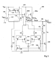
- FIG. 1 illustrates a first embodiment of a low drop-out (LDO) voltage regulating circuit 100.
- LDO circuit 100 comprises a P-channel MOS transistor (PMOS) 102 having its source terminal connected to an input voltage V IN on line 104 and its drain terminal connected to a first terminal of a shunt resistor R SHUNT .
- the second terminal of the shunt resistor is connected to the output line 106 of the LDO circuit 100.
- a pass current I PASS flows through PMOS 102 and through the shunt resistor.
- the output voltage V OUT of the LDO circuit on line 106 in this first embodiment is equal to V IN minus the voltage between the drain and source of PMOS 102, minus the voltage drop across the shunt resistor.
- a comparator 108 provides a control signal to the gate terminal of PMOS 102. Comparator 108 receives a feedback voltage V f .
- Two resistors R1 and R2 are connected in series between the output line 106 and a ground node. A node 109 between resistors R1 and R2 provides the feedback voltage V f .
- a reference voltage V REF is also provided to comparator 108 on line 110, this voltage indicating the required output voltage V OUT .
- V REF could be a fixed voltage if the same output voltage is always required, or could be variable to allow the output voltage V OUT of the LDO circuit 100 to be varied during use.
- V REF and V f are provided to the gate terminals of transistors 112, 114 respectively of comparator 108.
- Transistors 112, 114 are N-channel MOS transistors having their source terminals connected to ground via a current source 119. Drain terminals of transistors 112, 114 are connected to respective drain terminals of further transistors 116, 118.
- Transistors 116, 118 are P-channel MOS transistors having their source terminals connected to line 104. The gates of transistors 116, 118 are connected together and to a node between the drain terminals of transistors 114, 118. The gate terminal of PMOS 102 is connected to the node between the drain terminals of transistors 112, 116.
- an N-channel MOS transistor (NMOS) 120 is connected between the output line 106 and ground that conducts a current I A .
- the drain terminal of NMOS 120 is connected to the output line 106 and the source terminal of NMOS 120 is connected to ground.
- a comparator 121 comprises four transistors 122, 124, 126, 128, for providing a control voltage to the gate terminal of NMOS 120.
- Comparator 121 compares the voltage drop across the shunt resistor R SHUNT with a reference voltage V A and varies the control signal to NMOS 120 such that the voltage across the shunt resistor is relatively constant, and equal to V A .
- a voltage source 130 providing voltage V A is connected between the first terminal of the shunt resistor and the gate terminal of transistor 122.
- the gate terminal of transistor 124 is connected to the output line 106, and thus to the second terminal of the shunt resistor.
- Transistors 122, 124 are P-channel MOS transistors having their source terminals connected together and to a common current source 132, and their drain terminals connected to the drain terminals of transistors 126, 128 respectively.
- Transistors 126, 128 are N-channel MOS transistors having their source terminals connected together and to a ground node. Furthermore, the gate terminals of transistors 126, 128 are connected together and to the node between the drain terminals of transistors 124, 128. The node 129 between the drain terminals of transistors 122, 126 is connected to the gate terminal of NMOS 120.
- comparator 108 provides a control signal to the gate terminal of PMOS 102 controlling PMOS 102 such that the feedback voltage V f equals the reference voltage V REF , resulting in the required output voltage V OUT .
- comparator 121 provides a control signal to the gate terminal of NMOS 120 such that the voltage drop across R SHUNT is equal to V A' thus ensuring that the current through R SHUNT and thus also through PMOS 102, remains relatively constant.
- the load current changes rapidly, for example in a step from 2 mA to 10 mA, the voltage across R SHUNT will suddenly increase above V A .
- NMOS 120 being a relatively fast device compared to PMOS 102, an increase in load current can therefore be compensated much more quickly than if PMOS 102 alone responded. Likewise, a rapid reduction in load current will result in an increased voltage V OUT at the output of the LDO circuit, which can be quickly compensated by control of NMOS 120 such that more current I A is conducted to ground.
- NMOS 120 is arranged to conduct a current I A to ground thus reducing the current I PASS such that the output current I OUT matches the required load current.
- I PASS is preferably at least as high as the highest load current required by the load, and the value of R SHUNT and V A are preferably selected to provide I PASS accordingly. For example, if the highest load current required is 20 mA, a resistance value of 5 ohms could be chosen for R SHUNT' and V A could be chosen to be 0.1 V to maintain the pass current at 20 mA.
- R SHUNT is preferably chosen to be relatively low, for example less than 10 ohms, to prevent a large voltage drop, as the voltage drop across this resistor combined with the source-drain voltage across PMOS 102 together define the minimum voltage drop achievable by the LDO circuit 100.
- FIG. 2 illustrates an alternative embodiment of an LDO circuit 200.
- a large proportion of the circuitry of LDO circuit 200 is the same as the circuitry of LDO circuit 100 of Figure 1 , and the common parts have been labelled with the same reference numerals and will not be described again in detail.
- NMOS 120 is replaced by a current control block 220 comprising a pair of transistors PMOS 220a and NMOS 220b, and a class AB control block 220c.
- the drain terminals of transistors 220a, 220b are connected together and to the output line 106.
- the source terminal of PMOS 220a is connected to V IN on line 104.
- the source terminal of NMOS 220b is connected to ground.
- Class AB control block 220 also comprises an input line connected to node 129 between the drain terminals of transistors 122, 126, and thus receives an input voltage signal from comparator 121.
- the voltage source 130 of Figure 1 is replaced in the circuit of Figure 2 by a voltage source 230 providing a voltage V B between the gate of transistor 122 and the first terminal of the shunt resistor.
- LDO circuit 200 of Figure 2 Operation of LDO circuit 200 of Figure 2 is similar to that of LDO circuit 100, except that current control block 220 allows current to be either routed from the output line 106 to ground, or provided to output line 106 from the supply line 104.
- current I A always flows from the output line 106 through NMOS 120 to ground
- current I A can either flow from output line 106 through NMOS 220b to ground, or from the supply line 104 through PMOS 220a to output line 106, and in particular to the load.
- Comparators 108, 121 function in the same way as described in relation to Figure 1 , except that voltage V B provided by the voltage source 230 is lower than V A of the LDO circuit 100, and preferably results in a current through the shunt resistor, and therefore also through PMOS 102, that is half way between the highest and lowest load currents required by the load. For example, if the maximum load current required is 50 mA, and the minimum is 10 mA, the pass current is preferably maintained at approximately 30 mA. If R SHUNT is for example chosen to be 5 ohms, V B is preferably therefore selected to be 0,15 V. In alternative embodiments however, V B could also be selected to be at a different value, depending on how the LDO circuit is to be loaded.
- Class AB control block 220c comprises circuitry for generating the appropriate control signals for driving transistors 220a and 220b based on the voltage at node 129.
- Type class AB circuits are generally well known, and variations in their design and operation are possible.
- class AB control block 220 is preferably arranged to control both PMOS 220a and NMOS 220b with voltage signals that follow changes in the voltage at node 129, in other words such that when the voltage at node 129 increases, the voltage provided to the gate of PMOS 220a and/or NMOS 220b increases, and when the voltage at node 129 decreases, the voltage at the gate of PMOS 220a and/or NMOS 220b decreases.
- the particular voltage levels provided to the gate terminals of PMOS 220a and NMOS 220b will depend on the particular characteristics of each device, and the supply voltage V IN on line 104.
- the voltage V Gb at the gate of NMOS 220b is equal to the voltage V c at node 129
- both PMOS 220a and NMOS 220b do not conduct at the same time, as this would imply that current is flowing from supply line 104 through NMOS 220a and PMOS 220b straight to ground.
- LDO circuit 200 is advantageous in that the current through PMOS 102 does not need to be maintained at a high level, but can instead be maintained at a lower level, thus reducing the power consumption of the circuit.
- the circuit still includes an NMOS transistor for regulating the current, providing a fast response to changes in the output voltage V OUT .
- the load current is increased from a value of I A below I PASS , to a value above I PASS' the output current I OUT can be quickly increased to I PASS by the control of NMOS 220b, which will stop conducting an thus prevent I A conducting to ground.
- the increase from I PASS to the required current level is provided by PMOS 220a, which is controlled at the same time to conduct current from supply line 104. If, on the other hand, the output current is to be rapidly reduced, this can be achieved quickly by control of NMOS 220b, which will quickly increase the current I A routed to ground.
- FIG. 3 illustrates an alternative embodiment of an LDO circuit 300.
- LDO circuit 300 comprises many of the same circuit elements as LDO circuit 100 of Figure 1 , and the common parts have been labelled with the same reference numerals and will not be described again in detail.
- PMOS 102 is replaced by PMOS transistors 302a and 302b, each connected in the same way as PMOS 102, with their source terminals connected to supply line 104, and their gate terminals connected to the node between the drain terminals of transistors 116 and 112.
- PMOS 302a is a larger device than PMOS 302b, and thus conducts more current.
- PMOS 302a is approximately 50 times larger than PMOS 302b, such that I PASSa through PMOS 302a is approximately 50 times greater than I PASSb though PMOS 302b.
- the drain terminal of PMOS 302a is connected directly to the output line 106, whereas the drain terminal of PMOS 302b is connected to the first terminal of the shunt resistor R SHUNT .
- the second terminal of R SHUNT is connected to output line 106. In this way, the current through R SHUNT is approximately 50 times less than the total pass current I PASS' which is equal to I PASSa + I PASSb .
- the shunt resistor R SHUNT of Figure 3 can thus have a resistance approximately 50 times larger than the shunt resistor R SHUNT of Figure 1 , for the same voltage drop across this resistor.
- R SHUNT of Figure 3 could have the same resistance as R SHUNT of Figure 1 , and would thus cause a much lower voltage drop.
- different ratios between the PMOS pass devices 302a, 302b could be chosen.
- Comparator 321 comprises resistors R3 and R4 with their first terminals connected to the first and second terminals of R SHUNT respectively. These resistors preferably have relatively high resistance values such that current through these resistors is kept low.
- the second terminal of R3 is connected to the source terminals of transistors 322, 324.
- Transistors 322, 324 are P-channel MOS transistors having their gate terminals connected together.
- the second terminal of R4 is connected to the source terminals of transistors 326, 328.
- Transistors 326, 328 are P-channel MOS transistors having their gate terminals connected together.
- the drain terminal of transistor 322 is connected to the drain terminal of an N-channel MOS transistor 330.
- the gate terminal of transistor 330 is connected to its drain terminal, and its source terminal is connected to ground.
- the drain terminal of transistor 324 is connected to its gate terminal and to a current source 332.
- the drain terminal of transistor 326 is connected to its gate terminal and to the current source 332.
- the drain terminal of transistor 328 is connected to the drain terminal of a further NMOS transistor 334, which has its gate terminal connected to the gate terminal of transistor 330, and its source terminal connected to ground.
- the gate terminal of NMOS 120 is connected to the drain terminals of transistors 334 and 328.
- comparator 321 of Figure 3 operates in a similar fashion to comparator 121 of Figure 1 , in that a relatively constant voltage is maintained across the shunt resistor R SHUNT
- comparator 321 comprises resistors R3 and R4 of different values to provide the required voltage different across the shunt resistor, rather than a voltage source 130.
- R3 is equal to approximately 2500 ohms and R4 is equal to approximately 250 ohms.
- comparator 321 of Figure 3 An advantage with comparator 321 of Figure 3 is that no part of this comparator needs to be connected to a supply source that is higher than the voltage V IN at the supply line 104.
- LDO circuitry having a pass device controlled to control the voltage at the output of the LDO circuit, and a current regulating device for regulating the current through the pass device such that the current remains relatively constant.
- a pass device that is used to control the voltage at the output of the device, and a separate current regulating means, an improved response time can be achieved.
- the current regulating means comprises a transistor that has a relatively fast response time when compared to the pass device.
- the current regulating means comprises an n-channel MOS transistor or an NPN bipolar junction transistor.
- Embodiments of LDO voltage regulators as described herein can for example be implemented in integrated circuit boards and used in a wide range of devices in which a rapid LDO regulating circuit is required.
- a PMOS transistor is used as the pass device.
- a PMOS device can be controlled at its gate terminal with a voltage that is lower than the voltage at its source terminal (connected to the supply voltage), and therefore small voltage drops can be provided by the LDO voltage regulator with no extra circuitry being required to achieve a gate voltage that is higher than the supply voltage.
- the current regulating device is preferably controlled based on maintaining the voltage drop across a resistor connected between the pass device and the output of the regulator.
- the pass device comprises a plurality of PMOS transistors connected in parallel, one of these PMOS transistors connected directly to the output of said LDO circuit and arranged to receive a comparatively large proportion of the pass current, and the other connected to the resistor.
- the resistor thus receives a relatively smaller portion of the pass current, and will cause a smaller voltage drop at the output of the LDO circuit.
- the pass device and current regulating means comprise MOS transistors, for example MOSFETs.
- MOS transistors for example MOSFETs.
- the principles of the present invention apply equally to bipolar junction transistors as they do to MOS transistors, and in particular an NPN bipolar junction transistor has a faster response time than a PNP bipolar junction transistor.
- one or more PMOS, NMOS or alternative transistors such as NPN or PNP bipolar junction transistors could be used as the pass device 102, 302a, 302b, or the current regulating device 120, 220a, 220b.
- NMOS transistors could be replaced by NPN bipolar transistors
- PMOS transistors could be replaced by PNP bipolar transistors.
- one or more small capacitors could be provided at the output of the LDO circuit for providing further voltage fluctuation compensation.
- Alternative comparator circuits could also be used.
- the voltage sources 130, 230 of Figures 1 and 2 and the resistance values of resistors R3 and R4 of Figure 3 are variable such that the pass current I PASS can be varied during use of the LDO circuit.
Landscapes
- Engineering & Computer Science (AREA)
- Physics & Mathematics (AREA)
- Electromagnetism (AREA)
- General Physics & Mathematics (AREA)
- Radar, Positioning & Navigation (AREA)
- Automation & Control Theory (AREA)
- Continuous-Control Power Sources That Use Transistors (AREA)
Description
- The present invention relates to a low drop-out voltage regulator and in particular to a low drop-out voltage regulator having a fast response time.
- Low drop-out (LDO) voltage regulators are used when a steady voltage level is required that is lower than the supply voltage level. It is necessary for such regulators to be able to provide a steady voltage level at the same time as providing the required current to a load.
- A P-channel MOS transistor (PMOS) is generally used in LDO voltage regulators as the pass device connected between the supply voltage and the load connected to the output of the LDO circuit. This PMOS is then controlled by control circuitry to perform the role of providing the required voltage level, for whatever current is required by the load.
- Depending on the type of load, the current required by the load may vary. A problem occurs in some known LDO circuits when the load current is required to vary rapidly. This is because the PMOS pass device is generally a relatively slow device, having a slow response to changes in the control signal provided at its gate terminal. This slow response results in the output voltage of the LDO circuit fluctuating, which is undesirable as this generates noise, and causes problems at high frequencies.
- In order to minimize the voltage fluctuations at the output of known LDO voltage regulators, an output capacitor is often provided. However, the output capacitor is required to be relatively large in order to adequately minimize voltage fluctuations, for example in the range of 0,5 µF to 10 µF depending on the scale of current variations. The necessity to provide such a large capacitor is disadvantageous as an additional discrete component is required that adds to the cost of manufacturing the device.
-
US Patent 6,333,623 discloses a low drop-out voltage regulator having an output stage with a pass device and a discharge device. The pass device and the discharge device are both controlled through a single feed back loop. - European Patent Application
1,365,302 discloses a low drop-out regulator configured to provide a high output current with a fast response. - Embodiments of the present invention aim to at least partially address some of the above-mentioned problems.
- According to a first aspect of the present invention, there is provided a low drop-out DC voltage regulator for regulating a voltage from a DC supply comprising: a pass device controllable to maintain a required voltage at an output of the regulator and arranged to provide a first current from the DC supply, at least part of said first current being provided to a load connected to the output of the regulator; and current regulating means connected to said pass device and to the output of the regulator, said current regulating means arranged to conduct a second current controlled such that the first current through said pass device remains constant irrespective of variations in a load current to said load.
- According to one embodiment of the present invention, resistance means are provided connected to the pass device and arranged to receive at least part of the first current, the current regulating means being controlled based on a voltage drop across the resistance means.
- According to a further aspect of the present invention, there is provided a method of regulating a voltage at the output of a low drop-out DC voltage regulator comprising: controlling a pass device to maintain a required voltage at the output of the regulator, the pass device providing a first current from the DC supply, at least part of the first current being provided to a load connected to the output of the regulator; and controlling a current regulating means connected to said pass device to conduct a second current controlled such that the first current through said pass device remains constant irrespective of a load current to said load.
- The foregoing and other purposes, features, aspects and advantages of the invention will become apparent from the following detailed description of embodiments, given by way of illustration and not limitation with reference to the accompanying drawings, in which:
-
Figures 1, 2 and3 illustrate LDO circuits according to first, second and third embodiments of the present invention respectively. -
Figure 1 illustrates a first embodiment of a low drop-out (LDO) voltage regulatingcircuit 100.LDO circuit 100 comprises a P-channel MOS transistor (PMOS) 102 having its source terminal connected to an input voltage VIN online 104 and its drain terminal connected to a first terminal of a shunt resistor RSHUNT. The second terminal of the shunt resistor is connected to theoutput line 106 of theLDO circuit 100. A pass current IPASS flows throughPMOS 102 and through the shunt resistor. The output voltage VOUT of the LDO circuit online 106 in this first embodiment is equal to VIN minus the voltage between the drain and source ofPMOS 102, minus the voltage drop across the shunt resistor. - A
comparator 108 provides a control signal to the gate terminal ofPMOS 102.Comparator 108 receives a feedback voltage Vf. Two resistors R1 and R2 are connected in series between theoutput line 106 and a ground node. Anode 109 between resistors R1 and R2 provides the feedback voltage Vf. A reference voltage VREF is also provided tocomparator 108 online 110, this voltage indicating the required output voltage VOUT. VREF could be a fixed voltage if the same output voltage is always required, or could be variable to allow the output voltage VOUT of theLDO circuit 100 to be varied during use. - VREF and Vf are provided to the gate terminals of
transistors comparator 108.Transistors current source 119. Drain terminals oftransistors further transistors Transistors line 104. The gates oftransistors transistors transistors - According to this first embodiment, an N-channel MOS transistor (NMOS) 120 is connected between the
output line 106 and ground that conducts a current IA. The drain terminal ofNMOS 120 is connected to theoutput line 106 and the source terminal ofNMOS 120 is connected to ground. Acomparator 121 comprises fourtransistors NMOS 120.Comparator 121 compares the voltage drop across the shunt resistor RSHUNT with a reference voltage VA and varies the control signal toNMOS 120 such that the voltage across the shunt resistor is relatively constant, and equal to VA.A voltage source 130 providing voltage VA is connected between the first terminal of the shunt resistor and the gate terminal oftransistor 122. The gate terminal oftransistor 124 is connected to theoutput line 106, and thus to the second terminal of the shunt resistor.Transistors current source 132, and their drain terminals connected to the drain terminals oftransistors Transistors transistors transistors node 129 between the drain terminals oftransistors NMOS 120. - In operation,
comparator 108 provides a control signal to the gate terminal ofPMOS 102 controllingPMOS 102 such that the feedback voltage Vf equals the reference voltage VREF, resulting in the required output voltage VOUT. At the same time,comparator 121 provides a control signal to the gate terminal ofNMOS 120 such that the voltage drop across RSHUNT is equal to VA' thus ensuring that the current through RSHUNT and thus also throughPMOS 102, remains relatively constant. When the load current changes rapidly, for example in a step from 2 mA to 10 mA, the voltage across RSHUNT will suddenly increase above VA. This will in turn causetransistor 124 ofcomparator 121 to conduct more thantransistor 122, causing the voltage at the drain terminals oftransistors NMOS 120. The current IA throughNMOS 120 will thus drop, and more of the pass current IPASS throughPMOS 102 will be provided to the load at theoutput line 106. This effect will continue until the required load current has been satisfied, and the voltage across the shunt resistor has returned to VA. NMOS 120 being a relatively fast device compared toPMOS 102, an increase in load current can therefore be compensated much more quickly than ifPMOS 102 alone responded. Likewise, a rapid reduction in load current will result in an increased voltage VOUT at the output of the LDO circuit, which can be quickly compensated by control ofNMOS 120 such that more current IA is conducted to ground. - According to the embodiment of
Figure 1 ,NMOS 120 is arranged to conduct a current IA to ground thus reducing the current IPASS such that the output current IOUT matches the required load current. Thus IPASS is preferably at least as high as the highest load current required by the load, and the value of RSHUNT and VA are preferably selected to provide IPASS accordingly. For example, if the highest load current required is 20 mA, a resistance value of 5 ohms could be chosen for RSHUNT' and VA could be chosen to be 0.1 V to maintain the pass current at 20 mA. The value of RSHUNT is preferably chosen to be relatively low, for example less than 10 ohms, to prevent a large voltage drop, as the voltage drop across this resistor combined with the source-drain voltage acrossPMOS 102 together define the minimum voltage drop achievable by theLDO circuit 100. -
Figure 2 illustrates an alternative embodiment of an LDOcircuit 200. A large proportion of the circuitry ofLDO circuit 200 is the same as the circuitry ofLDO circuit 100 ofFigure 1 , and the common parts have been labelled with the same reference numerals and will not be described again in detail. In LDOcircuit 200,NMOS 120 is replaced by acurrent control block 220 comprising a pair oftransistors PMOS 220a andNMOS 220b, and a classAB control block 220c. The drain terminals oftransistors output line 106. The source terminal of PMOS 220a is connected to VIN online 104. The source terminal ofNMOS 220b is connected to ground. The gate terminals oftransistors AB control block 220c. Class AB control block 220 also comprises an input line connected tonode 129 between the drain terminals oftransistors comparator 121. - The
voltage source 130 ofFigure 1 is replaced in the circuit ofFigure 2 by avoltage source 230 providing a voltage VB between the gate oftransistor 122 and the first terminal of the shunt resistor. - Operation of
LDO circuit 200 ofFigure 2 is similar to that ofLDO circuit 100, except thatcurrent control block 220 allows current to be either routed from theoutput line 106 to ground, or provided tooutput line 106 from thesupply line 104. Thus whereas in the circuit ofFigure 1 current IA always flows from theoutput line 106 throughNMOS 120 to ground, in the circuit ofFigure 2 current IA can either flow fromoutput line 106 throughNMOS 220b to ground, or from thesupply line 104 throughPMOS 220a tooutput line 106, and in particular to the load. -
Comparators Figure 1 , except that voltage VB provided by thevoltage source 230 is lower than VA of theLDO circuit 100, and preferably results in a current through the shunt resistor, and therefore also throughPMOS 102, that is half way between the highest and lowest load currents required by the load. For example, if the maximum load current required is 50 mA, and the minimum is 10 mA, the pass current is preferably maintained at approximately 30 mA. If RSHUNT is for example chosen to be 5 ohms, VB is preferably therefore selected to be 0,15 V. In alternative embodiments however, VB could also be selected to be at a different value, depending on how the LDO circuit is to be loaded. - Class
AB control block 220c comprises circuitry for generating the appropriate control signals for drivingtransistors node 129. Type class AB circuits are generally well known, and variations in their design and operation are possible. In the present case, classAB control block 220 is preferably arranged to control bothPMOS 220a andNMOS 220b with voltage signals that follow changes in the voltage atnode 129, in other words such that when the voltage atnode 129 increases, the voltage provided to the gate ofPMOS 220a and/orNMOS 220b increases, and when the voltage atnode 129 decreases, the voltage at the gate ofPMOS 220a and/orNMOS 220b decreases. The particular voltage levels provided to the gate terminals ofPMOS 220a andNMOS 220b will depend on the particular characteristics of each device, and the supply voltage VIN online 104. In one example, the voltage VGb at the gate ofNMOS 220b is equal to the voltage Vc atnode 129, and the voltage VGa at the gate ofPMOS 220a is as follows:
where Vc is the voltage atnode 129, and VT is the absolute value of the threshold voltage ofPMOS 220a andNMOS 220b. Preferably bothPMOS 220a andNMOS 220b do not conduct at the same time, as this would imply that current is flowing fromsupply line 104 throughNMOS 220a andPMOS 220b straight to ground. -
LDO circuit 200 is advantageous in that the current throughPMOS 102 does not need to be maintained at a high level, but can instead be maintained at a lower level, thus reducing the power consumption of the circuit. The circuit still includes an NMOS transistor for regulating the current, providing a fast response to changes in the output voltage VOUT. In particular, if the load current is increased from a value of IA below IPASS, to a value above IPASS' the output current IOUT can be quickly increased to IPASS by the control ofNMOS 220b, which will stop conducting an thus prevent IA conducting to ground. The increase from IPASS to the required current level is provided byPMOS 220a, which is controlled at the same time to conduct current fromsupply line 104. If, on the other hand, the output current is to be rapidly reduced, this can be achieved quickly by control ofNMOS 220b, which will quickly increase the current IA routed to ground. -
Figure 3 illustrates an alternative embodiment of anLDO circuit 300.LDO circuit 300 comprises many of the same circuit elements asLDO circuit 100 ofFigure 1 , and the common parts have been labelled with the same reference numerals and will not be described again in detail. As shown inFigure 3 ,PMOS 102 is replaced byPMOS transistors PMOS 102, with their source terminals connected to supplyline 104, and their gate terminals connected to the node between the drain terminals oftransistors PMOS 302a is a larger device thanPMOS 302b, and thus conducts more current. In the present example,PMOS 302a is approximately 50 times larger thanPMOS 302b, such that IPASSa throughPMOS 302a is approximately 50 times greater than IPASSb thoughPMOS 302b. The drain terminal ofPMOS 302a is connected directly to theoutput line 106, whereas the drain terminal ofPMOS 302b is connected to the first terminal of the shunt resistor RSHUNT. The second terminal of RSHUNT is connected tooutput line 106. In this way, the current through RSHUNT is approximately 50 times less than the total pass current IPASS' which is equal to IPASSa + IPASSb. The shunt resistor RSHUNT ofFigure 3 can thus have a resistance approximately 50 times larger than the shunt resistor RSHUNT ofFigure 1 , for the same voltage drop across this resistor. Alternatively, RSHUNT ofFigure 3 could have the same resistance as RSHUNT ofFigure 1 , and would thus cause a much lower voltage drop. In alternative embodiments, different ratios between thePMOS pass devices - As with
LDO circuit 100 ofFigure 1 ,NMOS 120 inFigure 3 is controlled by regulating the voltage drop across RSHUNT, however analternative comparator circuit 321 is provided in place ofcomparator 121.Comparator 321 comprises resistors R3 and R4 with their first terminals connected to the first and second terminals of RSHUNT respectively. These resistors preferably have relatively high resistance values such that current through these resistors is kept low. The second terminal of R3 is connected to the source terminals oftransistors Transistors transistors Transistors transistor 322 is connected to the drain terminal of an N-channel MOS transistor 330. The gate terminal oftransistor 330 is connected to its drain terminal, and its source terminal is connected to ground. The drain terminal oftransistor 324 is connected to its gate terminal and to acurrent source 332. Likewise, the drain terminal oftransistor 326 is connected to its gate terminal and to thecurrent source 332. The drain terminal oftransistor 328 is connected to the drain terminal of afurther NMOS transistor 334, which has its gate terminal connected to the gate terminal oftransistor 330, and its source terminal connected to ground. The gate terminal ofNMOS 120 is connected to the drain terminals oftransistors - In operation,
comparator 321 ofFigure 3 operates in a similar fashion tocomparator 121 ofFigure 1 , in that a relatively constant voltage is maintained across the shunt resistor RSHUNT However,comparator 321 comprises resistors R3 and R4 of different values to provide the required voltage different across the shunt resistor, rather than avoltage source 130. For example, in one embodiment R3 is equal to approximately 2500 ohms and R4 is equal to approximately 250 ohms. If, for example, the output current IOUT increases, the current IPASS will also increase, causing an increase in the voltage across the shunt resistor RSHUNT. In consequence, the current throughtransistors transistors transistor 120 to drop, thus reducing the current IA. This reduces the increase in current IPASS, in other words keeping IPASS constant. - An advantage with
comparator 321 ofFigure 3 is that no part of this comparator needs to be connected to a supply source that is higher than the voltage VIN at thesupply line 104. - Thus LDO circuitry has been described having a pass device controlled to control the voltage at the output of the LDO circuit, and a current regulating device for regulating the current through the pass device such that the current remains relatively constant. By providing a pass device that is used to control the voltage at the output of the device, and a separate current regulating means, an improved response time can be achieved. Preferably the current regulating means comprises a transistor that has a relatively fast response time when compared to the pass device. For example, the current regulating means comprises an n-channel MOS transistor or an NPN bipolar junction transistor.
- Embodiments of LDO voltage regulators as described herein can for example be implemented in integrated circuit boards and used in a wide range of devices in which a rapid LDO regulating circuit is required.
- Advantageously according to embodiments of the present invention a PMOS transistor is used as the pass device. A PMOS device can be controlled at its gate terminal with a voltage that is lower than the voltage at its source terminal (connected to the supply voltage), and therefore small voltage drops can be provided by the LDO voltage regulator with no extra circuitry being required to achieve a gate voltage that is higher than the supply voltage.
- The current regulating device is preferably controlled based on maintaining the voltage drop across a resistor connected between the pass device and the output of the regulator. In certain embodiments, the pass device comprises a plurality of PMOS transistors connected in parallel, one of these PMOS transistors connected directly to the output of said LDO circuit and arranged to receive a comparatively large proportion of the pass current, and the other connected to the resistor. The resistor thus receives a relatively smaller portion of the pass current, and will cause a smaller voltage drop at the output of the LDO circuit.
- Whilst a number of specific embodiments of LDO circuits have been described, it will be apparent that there are various modifications that could be applied. In particular, in alternative embodiments, the features described above in relation to any of the embodiments could be combined in any combination.
- Examples have been described in which the pass device and current regulating means comprise MOS transistors, for example MOSFETs. The principles of the present invention apply equally to bipolar junction transistors as they do to MOS transistors, and in particular an NPN bipolar junction transistor has a faster response time than a PNP bipolar junction transistor. In alternative embodiments, one or more PMOS, NMOS or alternative transistors such as NPN or PNP bipolar junction transistors could be used as the
pass device current regulating device Figures 1, 2 and3 , some or all of the NMOS transistors could be replaced by NPN bipolar transistors, and some or all of the PMOS transistors could be replaced by PNP bipolar transistors. Whilst not shown in the figures, in some embodiments one or more small capacitors could be provided at the output of the LDO circuit for providing further voltage fluctuation compensation. Alternative comparator circuits could also be used. - In some embodiments the
voltage sources Figures 1 and 2 and the resistance values of resistors R3 and R4 ofFigure 3 are variable such that the pass current IPASS can be varied during use of the LDO circuit. - Having thus described at least one illustrative embodiment of the invention, various alterations, modifications and improvements will readily occur to those skilled in the art. Such alterations, modifications and improvements are intended to be within the scope of the invention. Accordingly, the foregoing description is by way of example only and is not intended to be limiting. The invention is limited only as defined in the following claims and the equivalent thereto.
Claims (11)
- A low drop-out DC voltage regulator (100, 200, 300) for regulating a voltage from a DC supply (VIN) comprising:a pass device (102, 302a, 302b) controllable to maintain a required voltage at an output (106) of the regulator and-arranged to provide a first current (IPASS) from the DC supply, at least part of said first current being provided to a load connected to the output of the regulator; andcurrent regulating means (120, 220a, 220b) connected to said pass device and to the output of the regulator, characterized in that said current regulating means is arranged to conduct a second current (IA) controlled such that the first current through said pass device remains constant irrespective of variations in a load current to said load.
- The low drop-out DC voltage regulator of claim 1 wherein said controllable pass device comprises one of a P-channel MOS transistor (102, 302a, 302b) and a PNP bipolar junction transistor, and said current regulating means comprises one of an N-channel MOS transistor (120, 220b) and an NPN bipolar junction transistor.
- The low drop-out DC voltage regulator of claim 1 further comprising resistance means (RSHUNT) connected to the pass device and arranged to receive at least part of the first current, the current regulating means being controlled based on a voltage drop across the resistance means.
- The low drop-out DC voltage regulator of claim 3 wherein said current regulating means comprises a transistor (120, 220b) and said regulator further comprises a comparator (121, 321) connected to first and second terminals of said resistance means and to a gate terminal of said transistor, said comparator being arranged to provide a control signal to the gate terminal of said transistor for controlling said second current.
- The low drop-out DC voltage regulator of claim 1 further comprising a comparator (108) connected to the output of the regulator for controlling the pass device.
- The low drop-out DC voltage regulator of claim 1 wherein the first current comprises a load current to a load connected to the output of the regulator and said second current through said current regulating means.
- The low drop-out DC voltage regulator of claim 1 wherein said current regulating means is operable to provide said second current (IA) to said load or to receive said second current from said pass device.
- The low drop-out DC voltage regulator of claim 7 wherein said current regulating means comprises a first transistor (220a) and a second transistor (220b), said first transistor being connected to a high voltage level and the second transistor being connected to a low voltage level.
- A device comprising an integrated circuit comprising the low drop-out DC voltage regulator of any preceding claim.
- A method of regulating a voltage at the output of a low drop-out DC voltage regulator (100, 200, 300) comprising:controlling a pass device (102, 302a, 302b) to maintain a required voltage at the output of the regulator, the pass device providing a first current (IPASS) from the DC supply, at least part of the first current being provided to a load connected to the output of the regulator; and characterized in that the method comprises:controlling a current regulating means (120, 220a, 220b) connected to said pass device to conduct a second current (IA) controlled such that the first current through said pass device remains constant irrespective of a load current to said load.
- The method of claim 10 wherein said current regulating means is controlled based on the voltage drop across a resistance means (RSHUNT) connected between said pass device and the output of said regulator.
Priority Applications (2)
| Application Number | Priority Date | Filing Date | Title |
|---|---|---|---|
| EP06300559A EP1865397B1 (en) | 2006-06-05 | 2006-06-05 | Low drop-out voltage regulator |
| US11/757,865 US8044653B2 (en) | 2006-06-05 | 2007-06-04 | Low drop-out voltage regulator |
Applications Claiming Priority (1)
| Application Number | Priority Date | Filing Date | Title |
|---|---|---|---|
| EP06300559A EP1865397B1 (en) | 2006-06-05 | 2006-06-05 | Low drop-out voltage regulator |
Publications (2)
| Publication Number | Publication Date |
|---|---|
| EP1865397A1 EP1865397A1 (en) | 2007-12-12 |
| EP1865397B1 true EP1865397B1 (en) | 2012-11-21 |
Family
ID=36910935
Family Applications (1)
| Application Number | Title | Priority Date | Filing Date |
|---|---|---|---|
| EP06300559A Not-in-force EP1865397B1 (en) | 2006-06-05 | 2006-06-05 | Low drop-out voltage regulator |
Country Status (2)
| Country | Link |
|---|---|
| US (1) | US8044653B2 (en) |
| EP (1) | EP1865397B1 (en) |
Families Citing this family (19)
| Publication number | Priority date | Publication date | Assignee | Title |
|---|---|---|---|---|
| KR101369154B1 (en) * | 2007-12-11 | 2014-03-04 | 삼성전자주식회사 | Shunt regulator having over-voltage protection circuit and semiconductor device including the same |
| US9766642B2 (en) * | 2009-07-16 | 2017-09-19 | Telefonaktiebolaget Lm Ericsson (Publ) | Low-dropout regulator |
| JP5361614B2 (en) * | 2009-08-28 | 2013-12-04 | ルネサスエレクトロニクス株式会社 | Buck circuit |
| WO2013137910A1 (en) | 2012-03-16 | 2013-09-19 | Tseng Richard Y | A low-impedance reference voltage generator |
| US9122293B2 (en) | 2012-10-31 | 2015-09-01 | Qualcomm Incorporated | Method and apparatus for LDO and distributed LDO transient response accelerator |
| US9170590B2 (en) | 2012-10-31 | 2015-10-27 | Qualcomm Incorporated | Method and apparatus for load adaptive LDO bias and compensation |
| US9235225B2 (en) | 2012-11-06 | 2016-01-12 | Qualcomm Incorporated | Method and apparatus reduced switch-on rate low dropout regulator (LDO) bias and compensation |
| US8981745B2 (en) | 2012-11-18 | 2015-03-17 | Qualcomm Incorporated | Method and apparatus for bypass mode low dropout (LDO) regulator |
| CN104142701B (en) | 2013-05-06 | 2016-08-24 | 意法半导体研发(深圳)有限公司 | Current-limiting circuit |
| EP2804067B1 (en) | 2013-05-17 | 2015-12-09 | Asahi Kasei Microdevices Corporation | Low output noise density low power ldo voltage regulator |
| US9436196B2 (en) * | 2014-08-20 | 2016-09-06 | Taiwan Semiconductor Manufacturing Company, Ltd. | Voltage regulator and method |
| KR20170003025A (en) * | 2015-06-30 | 2017-01-09 | 에스케이하이닉스 주식회사 | Internal voltage generation circuit |
| CN108885474B (en) * | 2016-03-25 | 2020-05-19 | 松下知识产权经营株式会社 | regulator circuit |
| US10133288B2 (en) * | 2016-09-30 | 2018-11-20 | Synopsys, Inc. | Circuit for low-dropout regulator output |
| WO2018228774A1 (en) | 2017-06-13 | 2018-12-20 | Firecomms Limited | A power efficient integrated circuit low output impedance voltage regulator |
| JP2019139445A (en) | 2018-02-08 | 2019-08-22 | ローム株式会社 | regulator |
| US11281248B2 (en) * | 2020-02-12 | 2022-03-22 | Nuvoton Technology Corporation | Audio microphone detection using auto-tracking current comparator |
| CN112218009A (en) * | 2020-09-28 | 2021-01-12 | 深圳市春盛海科技有限公司 | Noise reduction circuit for reducing image noise of image sensor |
| DE102020129614B3 (en) * | 2020-11-10 | 2021-11-11 | Infineon Technologies Ag | Voltage regulation circuit and method of operating a voltage regulation circuit |
Family Cites Families (21)
| Publication number | Priority date | Publication date | Assignee | Title |
|---|---|---|---|---|
| US5528127A (en) * | 1994-05-17 | 1996-06-18 | National Semiconductor Corporation | Controlling power dissipation within a linear voltage regulator circuit |
| JP2865133B2 (en) * | 1996-07-26 | 1999-03-08 | 日本電気株式会社 | Stabilized power supply circuit |
| US6304131B1 (en) * | 2000-02-22 | 2001-10-16 | Texas Instruments Incorporated | High power supply ripple rejection internally compensated low drop-out voltage regulator using PMOS pass device |
| US6452766B1 (en) * | 2000-10-30 | 2002-09-17 | National Semiconductor Corporation | Over-current protection circuit |
| US6333623B1 (en) | 2000-10-30 | 2001-12-25 | Texas Instruments Incorporated | Complementary follower output stage circuitry and method for low dropout voltage regulator |
| US6605931B2 (en) * | 2000-11-07 | 2003-08-12 | Microsemi Corporation | Switching regulator with transient recovery circuit |
| FR2819904B1 (en) * | 2001-01-19 | 2003-07-25 | St Microelectronics Sa | VOLTAGE REGULATOR PROTECTED AGAINST SHORT CIRCUITS |
| US6806690B2 (en) * | 2001-12-18 | 2004-10-19 | Texas Instruments Incorporated | Ultra-low quiescent current low dropout (LDO) voltage regulator with dynamic bias and bandwidth |
| US6677735B2 (en) * | 2001-12-18 | 2004-01-13 | Texas Instruments Incorporated | Low drop-out voltage regulator having split power device |
| US6703815B2 (en) * | 2002-05-20 | 2004-03-09 | Texas Instruments Incorporated | Low drop-out regulator having current feedback amplifier and composite feedback loop |
| US6989659B2 (en) * | 2002-09-09 | 2006-01-24 | Acutechnology Semiconductor | Low dropout voltage regulator using a depletion pass transistor |
| US6952091B2 (en) * | 2002-12-10 | 2005-10-04 | Stmicroelectronics Pvt. Ltd. | Integrated low dropout linear voltage regulator with improved current limiting |
| US6861827B1 (en) * | 2003-09-17 | 2005-03-01 | System General Corp. | Low drop-out voltage regulator and an adaptive frequency compensation |
| US6867573B1 (en) * | 2003-11-07 | 2005-03-15 | National Semiconductor Corporation | Temperature calibrated over-current protection circuit for linear voltage regulators |
| ITMI20041981A1 (en) * | 2004-10-19 | 2005-01-19 | St Microelectronics Srl | "DC / DC CONVERTER" |
| EP1910905B1 (en) * | 2005-07-21 | 2011-12-21 | Freescale Semiconductor, Inc. | Voltage regulator with pass transistors carrying different ratios of the total load current and method of operation therefor |
| US7173401B1 (en) * | 2005-08-01 | 2007-02-06 | Integrated System Solution Corp. | Differential amplifier and low drop-out regulator with thereof |
| US7109897B1 (en) * | 2005-10-07 | 2006-09-19 | Rf Micro Devices, Inc. | Power amplifier control reducing output power variation |
| EP1830238B1 (en) * | 2006-03-03 | 2011-12-14 | Dialog Semiconductor B.V. | Low dropout voltage regulator for slot-based operation |
| US7816897B2 (en) * | 2006-03-10 | 2010-10-19 | Standard Microsystems Corporation | Current limiting circuit |
| US7683592B2 (en) * | 2006-09-06 | 2010-03-23 | Atmel Corporation | Low dropout voltage regulator with switching output current boost circuit |
-
2006
- 2006-06-05 EP EP06300559A patent/EP1865397B1/en not_active Not-in-force
-
2007
- 2007-06-04 US US11/757,865 patent/US8044653B2/en active Active
Also Published As
| Publication number | Publication date |
|---|---|
| EP1865397A1 (en) | 2007-12-12 |
| US8044653B2 (en) | 2011-10-25 |
| US20080007231A1 (en) | 2008-01-10 |
Similar Documents
| Publication | Publication Date | Title |
|---|---|---|
| US8044653B2 (en) | Low drop-out voltage regulator | |
| US8129966B2 (en) | Voltage regulator circuit and control method therefor | |
| JP5008472B2 (en) | Voltage regulator | |
| US9645594B2 (en) | Voltage regulator with dropout detector and bias current limiter and associated methods | |
| KR101435238B1 (en) | Voltage regulator | |
| US9812958B2 (en) | Voltage regulator with improved overshoot and undershoot voltage compensation | |
| US8253404B2 (en) | Constant voltage circuit | |
| US10534390B2 (en) | Series regulator including parallel transistors | |
| US20130113454A1 (en) | Signal generating circuit | |
| JP2004005670A (en) | Low dropout regulator comprising current feedback amplifier and compound feedback loop | |
| US10331152B2 (en) | Quiescent current control in voltage regulators | |
| US7233462B2 (en) | Voltage regulator having overcurrent protection circuit | |
| US9831757B2 (en) | Voltage regulator | |
| KR20060047972A (en) | Voltage regulator | |
| US20180120875A1 (en) | Voltage regulator | |
| US10571941B2 (en) | Voltage regulator | |
| US8085006B2 (en) | Shunt regulator | |
| JP2017126259A (en) | Power supply | |
| CN110045777B (en) | Reverse current prevention circuit and power supply circuit | |
| US7362081B1 (en) | Low-dropout regulator | |
| US7816897B2 (en) | Current limiting circuit | |
| US9886052B2 (en) | Voltage regulator | |
| US8013582B2 (en) | Voltage control circuit | |
| JP7826900B2 (en) | Overcurrent detection circuit | |
| US8149063B2 (en) | Current-restriction circuit and driving method therefor |
Legal Events
| Date | Code | Title | Description |
|---|---|---|---|
| PUAI | Public reference made under article 153(3) epc to a published international application that has entered the european phase |
Free format text: ORIGINAL CODE: 0009012 |
|
| AK | Designated contracting states |
Kind code of ref document: A1 Designated state(s): AT BE BG CH CY CZ DE DK EE ES FI FR GB GR HU IE IS IT LI LT LU LV MC NL PL PT RO SE SI SK TR |
|
| AX | Request for extension of the european patent |
Extension state: AL BA HR MK YU |
|
| 17P | Request for examination filed |
Effective date: 20080612 |
|
| 17Q | First examination report despatched |
Effective date: 20080717 |
|
| AKX | Designation fees paid |
Designated state(s): DE FR GB IT |
|
| GRAP | Despatch of communication of intention to grant a patent |
Free format text: ORIGINAL CODE: EPIDOSNIGR1 |
|
| RIN1 | Information on inventor provided before grant (corrected) |
Inventor name: MAIGE, PHILIPPE Inventor name: GUEDON, YANNICK |
|
| GRAS | Grant fee paid |
Free format text: ORIGINAL CODE: EPIDOSNIGR3 |
|
| GRAA | (expected) grant |
Free format text: ORIGINAL CODE: 0009210 |
|
| AK | Designated contracting states |
Kind code of ref document: B1 Designated state(s): DE FR GB IT |
|
| REG | Reference to a national code |
Ref country code: GB Ref legal event code: FG4D |
|
| REG | Reference to a national code |
Ref country code: DE Ref legal event code: R096 Ref document number: 602006033182 Country of ref document: DE Effective date: 20130117 |
|
| PGFP | Annual fee paid to national office [announced via postgrant information from national office to epo] |
Ref country code: DE Payment date: 20130523 Year of fee payment: 8 |
|
| PG25 | Lapsed in a contracting state [announced via postgrant information from national office to epo] |
Ref country code: IT Free format text: LAPSE BECAUSE OF FAILURE TO SUBMIT A TRANSLATION OF THE DESCRIPTION OR TO PAY THE FEE WITHIN THE PRESCRIBED TIME-LIMIT Effective date: 20121121 |
|
| PLBE | No opposition filed within time limit |
Free format text: ORIGINAL CODE: 0009261 |
|
| STAA | Information on the status of an ep patent application or granted ep patent |
Free format text: STATUS: NO OPPOSITION FILED WITHIN TIME LIMIT |
|
| 26N | No opposition filed |
Effective date: 20130822 |
|
| PGFP | Annual fee paid to national office [announced via postgrant information from national office to epo] |
Ref country code: FR Payment date: 20130724 Year of fee payment: 8 |
|
| REG | Reference to a national code |
Ref country code: DE Ref legal event code: R097 Ref document number: 602006033182 Country of ref document: DE Effective date: 20130822 |
|
| GBPC | Gb: european patent ceased through non-payment of renewal fee |
Effective date: 20130605 |
|
| PG25 | Lapsed in a contracting state [announced via postgrant information from national office to epo] |
Ref country code: GB Free format text: LAPSE BECAUSE OF NON-PAYMENT OF DUE FEES Effective date: 20130605 |
|
| REG | Reference to a national code |
Ref country code: DE Ref legal event code: R119 Ref document number: 602006033182 Country of ref document: DE |
|
| REG | Reference to a national code |
Ref country code: DE Ref legal event code: R119 Ref document number: 602006033182 Country of ref document: DE Effective date: 20150101 |
|
| REG | Reference to a national code |
Ref country code: FR Ref legal event code: ST Effective date: 20150227 |
|
| PG25 | Lapsed in a contracting state [announced via postgrant information from national office to epo] |
Ref country code: DE Free format text: LAPSE BECAUSE OF NON-PAYMENT OF DUE FEES Effective date: 20150101 |
|
| PG25 | Lapsed in a contracting state [announced via postgrant information from national office to epo] |
Ref country code: FR Free format text: LAPSE BECAUSE OF NON-PAYMENT OF DUE FEES Effective date: 20140630 |