EP3412752B1 - Phosphor-including member, and light emitting device or projector - Google Patents
Phosphor-including member, and light emitting device or projector Download PDFInfo
- Publication number
- EP3412752B1 EP3412752B1 EP17747524.1A EP17747524A EP3412752B1 EP 3412752 B1 EP3412752 B1 EP 3412752B1 EP 17747524 A EP17747524 A EP 17747524A EP 3412752 B1 EP3412752 B1 EP 3412752B1
- Authority
- EP
- European Patent Office
- Prior art keywords
- phosphor
- single crystal
- particulate
- light
- yag
- Prior art date
- Legal status (The legal status is an assumption and is not a legal conclusion. Google has not performed a legal analysis and makes no representation as to the accuracy of the status listed.)
- Active
Links
Images


Classifications
-
- C—CHEMISTRY; METALLURGY
- C09—DYES; PAINTS; POLISHES; NATURAL RESINS; ADHESIVES; COMPOSITIONS NOT OTHERWISE PROVIDED FOR; APPLICATIONS OF MATERIALS NOT OTHERWISE PROVIDED FOR
- C09K—MATERIALS FOR MISCELLANEOUS APPLICATIONS, NOT PROVIDED FOR ELSEWHERE
- C09K11/00—Luminescent materials, e.g. electroluminescent or chemiluminescent
- C09K11/08—Luminescent materials, e.g. electroluminescent or chemiluminescent containing inorganic luminescent materials
- C09K11/77—Luminescent materials, e.g. electroluminescent or chemiluminescent containing inorganic luminescent materials containing rare earth metals
- C09K11/7766—Luminescent materials, e.g. electroluminescent or chemiluminescent containing inorganic luminescent materials containing rare earth metals containing two or more rare earth metals
- C09K11/7774—Aluminates
-
- C—CHEMISTRY; METALLURGY
- C01—INORGANIC CHEMISTRY
- C01F—COMPOUNDS OF THE METALS BERYLLIUM, MAGNESIUM, ALUMINIUM, CALCIUM, STRONTIUM, BARIUM, RADIUM, THORIUM, OR OF THE RARE-EARTH METALS
- C01F17/00—Compounds of rare earth metals
- C01F17/30—Compounds containing rare earth metals and at least one element other than a rare earth metal, oxygen or hydrogen, e.g. La4S3Br6
- C01F17/32—Compounds containing rare earth metals and at least one element other than a rare earth metal, oxygen or hydrogen, e.g. La4S3Br6 oxide or hydroxide being the only anion, e.g. NaCeO2 or MgxCayEuO
- C01F17/34—Aluminates, e.g. YAlO3 or Y3-xGdxAl5O12
-
- C—CHEMISTRY; METALLURGY
- C09—DYES; PAINTS; POLISHES; NATURAL RESINS; ADHESIVES; COMPOSITIONS NOT OTHERWISE PROVIDED FOR; APPLICATIONS OF MATERIALS NOT OTHERWISE PROVIDED FOR
- C09K—MATERIALS FOR MISCELLANEOUS APPLICATIONS, NOT PROVIDED FOR ELSEWHERE
- C09K11/00—Luminescent materials, e.g. electroluminescent or chemiluminescent
- C09K11/02—Use of particular materials as binders, particle coatings or suspension media therefor
-
- C—CHEMISTRY; METALLURGY
- C30—CRYSTAL GROWTH
- C30B—SINGLE-CRYSTAL GROWTH; UNIDIRECTIONAL SOLIDIFICATION OF EUTECTIC MATERIAL OR UNIDIRECTIONAL DEMIXING OF EUTECTOID MATERIAL; REFINING BY ZONE-MELTING OF MATERIAL; PRODUCTION OF A HOMOGENEOUS POLYCRYSTALLINE MATERIAL WITH DEFINED STRUCTURE; SINGLE CRYSTALS OR HOMOGENEOUS POLYCRYSTALLINE MATERIAL WITH DEFINED STRUCTURE; AFTER-TREATMENT OF SINGLE CRYSTALS OR A HOMOGENEOUS POLYCRYSTALLINE MATERIAL WITH DEFINED STRUCTURE; APPARATUS THEREFOR
- C30B29/00—Single crystals or homogeneous polycrystalline material with defined structure characterised by the material or by their shape
- C30B29/10—Inorganic compounds or compositions
- C30B29/16—Oxides
- C30B29/22—Complex oxides
- C30B29/28—Complex oxides with formula A3Me5O12 wherein A is a rare earth metal and Me is Fe, Ga, Sc, Cr, Co or Al, e.g. garnets
-
- C—CHEMISTRY; METALLURGY
- C30—CRYSTAL GROWTH
- C30B—SINGLE-CRYSTAL GROWTH; UNIDIRECTIONAL SOLIDIFICATION OF EUTECTIC MATERIAL OR UNIDIRECTIONAL DEMIXING OF EUTECTOID MATERIAL; REFINING BY ZONE-MELTING OF MATERIAL; PRODUCTION OF A HOMOGENEOUS POLYCRYSTALLINE MATERIAL WITH DEFINED STRUCTURE; SINGLE CRYSTALS OR HOMOGENEOUS POLYCRYSTALLINE MATERIAL WITH DEFINED STRUCTURE; AFTER-TREATMENT OF SINGLE CRYSTALS OR A HOMOGENEOUS POLYCRYSTALLINE MATERIAL WITH DEFINED STRUCTURE; APPARATUS THEREFOR
- C30B29/00—Single crystals or homogeneous polycrystalline material with defined structure characterised by the material or by their shape
- C30B29/60—Single crystals or homogeneous polycrystalline material with defined structure characterised by the material or by their shape characterised by shape
-
- C—CHEMISTRY; METALLURGY
- C30—CRYSTAL GROWTH
- C30B—SINGLE-CRYSTAL GROWTH; UNIDIRECTIONAL SOLIDIFICATION OF EUTECTIC MATERIAL OR UNIDIRECTIONAL DEMIXING OF EUTECTOID MATERIAL; REFINING BY ZONE-MELTING OF MATERIAL; PRODUCTION OF A HOMOGENEOUS POLYCRYSTALLINE MATERIAL WITH DEFINED STRUCTURE; SINGLE CRYSTALS OR HOMOGENEOUS POLYCRYSTALLINE MATERIAL WITH DEFINED STRUCTURE; AFTER-TREATMENT OF SINGLE CRYSTALS OR A HOMOGENEOUS POLYCRYSTALLINE MATERIAL WITH DEFINED STRUCTURE; APPARATUS THEREFOR
- C30B33/00—After-treatment of single crystals or homogeneous polycrystalline material with defined structure
-
- G—PHYSICS
- G03—PHOTOGRAPHY; CINEMATOGRAPHY; ANALOGOUS TECHNIQUES USING WAVES OTHER THAN OPTICAL WAVES; ELECTROGRAPHY; HOLOGRAPHY
- G03B—APPARATUS OR ARRANGEMENTS FOR TAKING PHOTOGRAPHS OR FOR PROJECTING OR VIEWING THEM; APPARATUS OR ARRANGEMENTS EMPLOYING ANALOGOUS TECHNIQUES USING WAVES OTHER THAN OPTICAL WAVES; ACCESSORIES THEREFOR
- G03B21/00—Projectors or projection-type viewers; Accessories therefor
- G03B21/14—Details
- G03B21/20—Lamp housings
- G03B21/2006—Lamp housings characterised by the light source
- G03B21/2033—LED or laser light sources
- G03B21/204—LED or laser light sources using secondary light emission, e.g. luminescence or fluorescence
-
- H—ELECTRICITY
- H01—ELECTRIC ELEMENTS
- H01S—DEVICES USING THE PROCESS OF LIGHT AMPLIFICATION BY STIMULATED EMISSION OF RADIATION [LASER] TO AMPLIFY OR GENERATE LIGHT; DEVICES USING STIMULATED EMISSION OF ELECTROMAGNETIC RADIATION IN WAVE RANGES OTHER THAN OPTICAL
- H01S5/00—Semiconductor lasers
- H01S5/02—Structural details or components not essential to laser action
- H01S5/022—Mountings; Housings
- H01S5/0239—Combinations of electrical or optical elements
-
- H—ELECTRICITY
- H10—SEMICONDUCTOR DEVICES; ELECTRIC SOLID-STATE DEVICES NOT OTHERWISE PROVIDED FOR
- H10H—INORGANIC LIGHT-EMITTING SEMICONDUCTOR DEVICES HAVING POTENTIAL BARRIERS
- H10H20/00—Individual inorganic light-emitting semiconductor devices having potential barriers, e.g. light-emitting diodes [LED]
- H10H20/80—Constructional details
- H10H20/85—Packages
- H10H20/851—Wavelength conversion means
- H10H20/8511—Wavelength conversion means characterised by their material, e.g. binder
- H10H20/8512—Wavelength conversion materials
-
- C—CHEMISTRY; METALLURGY
- C01—INORGANIC CHEMISTRY
- C01P—INDEXING SCHEME RELATING TO STRUCTURAL AND PHYSICAL ASPECTS OF SOLID INORGANIC COMPOUNDS
- C01P2002/00—Crystal-structural characteristics
- C01P2002/50—Solid solutions
- C01P2002/52—Solid solutions containing elements as dopants
-
- C—CHEMISTRY; METALLURGY
- C01—INORGANIC CHEMISTRY
- C01P—INDEXING SCHEME RELATING TO STRUCTURAL AND PHYSICAL ASPECTS OF SOLID INORGANIC COMPOUNDS
- C01P2004/00—Particle morphology
- C01P2004/01—Particle morphology depicted by an image
- C01P2004/03—Particle morphology depicted by an image obtained by SEM
-
- C—CHEMISTRY; METALLURGY
- C01—INORGANIC CHEMISTRY
- C01P—INDEXING SCHEME RELATING TO STRUCTURAL AND PHYSICAL ASPECTS OF SOLID INORGANIC COMPOUNDS
- C01P2004/00—Particle morphology
- C01P2004/60—Particles characterised by their size
- C01P2004/61—Micrometer sized, i.e. from 1-100 micrometer
-
- C—CHEMISTRY; METALLURGY
- C01—INORGANIC CHEMISTRY
- C01P—INDEXING SCHEME RELATING TO STRUCTURAL AND PHYSICAL ASPECTS OF SOLID INORGANIC COMPOUNDS
- C01P2006/00—Physical properties of inorganic compounds
- C01P2006/32—Thermal properties
- C01P2006/37—Stability against thermal decomposition
Definitions
- the invention relates to a phosphor and a production method thereof, a phosphor-including member, and a light-emitting device or a projector.
- a phosphor formed of YAG-based single crystal is known (see, e.g., JP 5,649,202 B ).
- the phosphor formed of the single crystal has excellent temperature characteristics in that a decrease in fluorescence intensity associated with temperature increase is less than ceramic powder phosphor.
- a light-emitting device which uses a particulate single crystal phosphor obtained by pulverizing a YAG-based single crystal ingot (see, e.g., JP 5,649,202 B and JP 5,620,562 B ).
- WO 2015/060254 A1 discloses a single-crystal phosphor which can exhibit excellent properties under high-temperature conditions; and a light-emitting device in which the phosphor is used.
- a single-crystal phosphor which has a chemical composition represented by the compositional formula: (Y 1-x-y-z Lu x Gd y Ce z ) 3+a Al 5-a O 12 (0 ⁇ x ⁇ 0.9994, 0 ⁇ y ⁇ 0.0669, 0.0002 ⁇ z ⁇ 0.0067, -0.016 ⁇ a ⁇ 0.315).
- WO 2015/060350 A1 discloses a YAG-based single crystal phosphor which produces fluorescence of a non-conventional color; and a phosphor-containing member and a light emitting device, each of which is provided with this single crystal phosphor.
- a single crystal phosphor which has a composition represented by composition formula (Y 1-a-b Lu a Ce b ) 3+c Al 5-c O1 2 (wherein 0 ⁇ a ⁇ 0.9994, 0.0002 ⁇ b ⁇ 0.0067 and -0.016 ⁇ c ⁇ 0.315), and which has an emission spectrum having CIE chromaticity coordinates x and y satisfying the relation -0.4377x + 0.7384 ⁇ y ⁇ -0.4585x + 0.7504 when the peak wavelength of the excitation light is 450 nm at the temperature of 25°C.
- ANASTASIYALATYNINAET AL "Properties of Czochralski grown Ce,Gd:Y3A15012 single crystal for white light-emitting diode", JOURNAL OF ALLOYS AND COMPOUNDS., vol. 553, 1 March 2013 (2013-03-01), pages 89-92, XP055532897, ISSN: 0925-8388, DOI: 10.1016/j.jallcom.2012.11.096 , discloses single crystal phosphor plates (SCPPs) using Czochralski grown Ce and Gd-doped Y 3 Al 5 O 12 (Ce,Gd:YAG) single crystal in a new concept of white LED. The new concept realizes epoxy resin free package and eliminates photodegradation issue. SCPP showed superior stability under the high temperatures, irradiation and current. Quantum efficiency of SCPP was found to be as high as 93%.
- a phosphor-including member comprising a particulate phosphor
- a phosphor-including member comprising a particulate phosphor
- the single crystal phosphor in the first embodiment is a YAG-based or LuAG-based single crystal phosphor of which base crystal is a Y 3 Al 5 O 12 (YAG)-based crystal or a Lu 3 Al 5 O 12 (LuAG)-based crystal and which has a composition represented by a compositional formula (Y 1-x-y-z Lu x Gd y Ce z ) 3+a Al 5-a O 12 ( 0 ⁇ x ⁇ 0.9994 , 0 ⁇ y ⁇ 0.0669 , 0.001 ⁇ z ⁇ 0.004 , - 0.016 ⁇ a ⁇ 0.315 ).
- Lu and Gd here are components which are substituted in the Y site but do not serve as emission centers.
- Ce is a component which can be substituted in the Y site and can serve as an emission center (an activator).
- composition of the single crystal phosphor some atoms may be in different positions in the crystal structure.
- composition ratio of O in the above compositional formula is 12
- the above-mentioned composition also includes compositions with an O composition ratio slightly different from 12 due to presence of inevitably mixed oxygen or oxygen deficiency.
- value of "a" in the compositional formula is a value which inevitably varies in the production of the single crystal phosphor, but variation within the numerical range of about -0.016 ⁇ a ⁇ 0.315 has little effect on physical properties of the single crystal phosphor.
- the phosphor in the first embodiment is characterized in that Group II elements such as Ba or Sr and Group XVII elements such as F or Br are not contained and purity is high. These characteristics allow the phosphor to have higher brightness and longer life.
- the reason why the numerical value of z representing the Ce concentration in the compositional formula is in a range of 0.001 ⁇ z ⁇ 0.004 is as follows: when the numerical value of z is less than 0.001, there is a problem that absorption by the particulate single crystal phosphor is reduced and external quantum efficiency is thus reduced, resulting in a decrease in emission intensity. On the other hand, when z is more than 0.004, high-temperature characteristics of the particulate single crystal phosphor degrade. For example, the internal quantum efficiency of phosphor at, e.g., 300 °C becomes less than 0.9.
- the Ce concentration of 0.001 ⁇ z ⁇ 0.004 is an optimized range for the particulate single crystal phosphor and is different from a Ce concentration range suitable for, e.g., a plate-shaped single crystal phosphor.
- the phosphor in the first embodiment is a particulate single crystal phosphor having a particle diameter (D 50 ) of not less than 20 ⁇ m.
- D 50 here is a particle diameter at 50 vol% in the cumulative distribution.
- the volume ratio of the phosphor to the material of the sealing member increases with increasing the particle diameter of the phosphor.
- Sealing material generally has a lower thermal conductivity than phosphor and thus causes thermal resistance to increase. Therefore, by increasing the volume ratio of the phosphor to the material of the sealing member, it is possible to reduce thermal resistance of the whole (the sealing member including the phosphor).
- the single crystalline YAG phosphor in the first embodiment is made by pulverizing a melt-grown ingot of single crystal phosphor, and thus can have even a particle diameter of not less than 100 ⁇ m.
- a material of the members coming into a contact with YAG, such as mills or balls, of the pulverizing equipment is preferably a material with high hardness, is most preferably a single crystalline YAG in view of contamination, but may be high-purity aluminum in view of productivity.
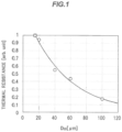
- FIG. 1 is a graph showing a relation between particle diameter (D 50 ) of YAG phosphor and thermal resistance.
- a point plotted at D 50 of 15 ⁇ m is data from a known sintered YAG phosphor, and other points are data from a particulate single crystalline YAG phosphor in the first embodiment (obtained by pulverizing a region of a single crystal phosphor ingot in which composition distribution is in a range from (Y 0.9990 Ce 0.0010 ) 3.175 Al 4.825 O x to (Y 0.9985 Ce 0.0015 ) 3.167 Al 4.833 O x ).
- thermal resistance of 100 ⁇ m-thick films containing the respective fluorescent bodies sealed with a SiO 2 -based inorganic sealing material indicates a relative value when the thermal resistance value of the sealing film with the known sintered YAG phosphor is defined as 1.
- the thickness of the sealing film containing a phosphor with D 50 of 100 ⁇ m is 110 ⁇ m.
- thermal resistance can be reduced less than that of when containing the known YAG sintered phosphor by adjusting a particle diameter (D 50 ) of the phosphor to 20 ⁇ m and can be reduced to half or less than half the thermal resistance of when containing the known YAG phosphor by adjusting to 60 ⁇ m.
- the present inventors also conducted experiments and confirmed that thermal resistance of a 100 ⁇ m-thick single crystalline YAG plate not containing a binder such as inorganic sealing material is about 0.1, and a particulate phosphor when having a particular size of about 100 to 120 ⁇ m can realize thermal resistance substantially equivalent to that of the single crystalline YAG plate.
- a decrease in fluorescence intensity associated with temperature increase is smaller in the YAG-based single crystal phosphor than in the YAG-based polycrystalline phosphor made by the sintering method, etc., as described previously.
- the small decrease in fluorescence intensity results from a small decrease in internal quantum efficiency. The same applies to the LuAG-based single crystal phosphor.
- the phosphor in the first embodiment is more suitable for use under high-temperature conditions due to having excellent emission properties under high-temperature conditions which are inherent to the YAG-based or LuAG-based single crystal phosphor, as well as due to having an effect of reducing thermal resistance of a phosphor-including member by controlling the particle diameter.
- the phosphor can be very functional when used in, e.g., a light-emitting device having very high brightness per unit area, such as laser projector or laser headlight using laser light as excitation light. Also, since the phosphor in the first embodiment is in the form of particles, it is effective to increase light scattering and it is thereby possible to realize more uniform emission intensity and emission color.
- the particle diameter (D 50 ) is preferably not more than 120 ⁇ m. This is because when more than 120 ⁇ m, yellow as a fluorescent color of the phosphor becomes too intense and it may be difficult to obtain white light with a desired chromaticity.
- the particulate phosphor is obtained by pulverizing a single crystal phosphor ingot grown by a method in which a crystal is pulled upward from a source melt, such as CZ method (Czochralski method), EFG method (Edge-Defined Film-Fed Growth Method) or Bridgman method.
- a single crystal phosphor is grown by the CZ method in the following example.
- powders of Y 2 O 3 , Lu 2 O 3 , Gd 2 O 3 , CeO 2 and Al 2 O 3 each having a high purity (not less than 99.99 % ) are prepared as starting materials and are dry-blended, thereby obtaining a mixture powder.
- the raw material powders of Y, Lu, Gd, Ce and Al are not limited to those mentioned above. Also, when producing a single crystal phosphor not containing Lu or Gd, the raw material powders thereof are not used.
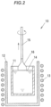
- FIG. 2 is a schematic cross-sectional view showing how a single crystal phosphor ingot is pulled upward in the CZ method.
- a crystal growth system 10 is provided primarily with an iridium crucible 11, a ceramic cylindrical container 12 housing the crucible 11, and a high-frequency coil 13 wound around the cylindrical container 12.
- the obtained mixture powder is loaded into the crucible 11, a high-frequency energy of 30 kW is supplied to the crucible 11 by the high-frequency coil 13 in a nitrogen atmosphere to generate an induced current, and the crucible 11 is thereby heated.
- the mixture powder is melted and a melt 14 is thereby obtained.
- a seed crystal 15 which is a YAG single crystal is prepared, the tip thereof is brought into contact with the melt 14, and the seed crystal 15 is pulled upward at a pulling rate of not more than 1 mm/h and rotated simultaneously at a rotation speed of 10 rpm at a pull-up temperature of not less than 1960° C, thereby growing a single crystal phosphor ingot 16 oriented to the ⁇ 111> direction.
- the single crystal phosphor ingot 16 is grown in a nitrogen atmosphere at atmospheric pressure in a state that nitrogen is being supplied at a flow rate of 2 L/min into the cylindrical container.
- the size of the single crystal phosphor ingot 16 is, e.g., about 2.5 cm in diameter and about 5 cm in length.
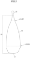
- Ce has a significantly larger ionic radius than Y in the YAG-based or LuAG-based single crystal as a base crystal and is thus less likely to be incorporated into the crystal. Therefore, when the YAG-based or LuAG-based single crystal phosphor is grown by a pulling-up method such as CZ (Czochralski) method, the Ce concentration in the source melt increases as the crystal grows, hence, the YAG-based or LuAG-based single crystal phosphor has a Ce concentration distribution gradient such that the Ce concentration decreases toward the direction of pulling up the crystal. In other words, the Ce concentration in the YAG-based or LuAG-based single crystal phosphor increases from the seed (the seed crystal) toward the tail.
- CZ Czochralski
- FIG. 3 is a schematic diagram illustrating the grown single crystal phosphor ingot 16. In the single crystal phosphor ingot 16, the Ce concentration increases from the seed crystal 15 toward a tail 17.
- a region of the single crystal phosphor ingot 16 in which z representing the Ce concentration in the compositional formula is, e.g., 0.001 ⁇ z ⁇ 0.004 is cut out as a pulverizing region 18.
- z representing the Ce concentration in the compositional formula is distributed continuously between 0.001 and 0.004 along the pull-up direction of the single crystal phosphor ingot 16.
- this continuity of Ce concentration distribution is relevant to the effective segregation coefficient defined by FIG. 3 and Formula 1 (see below) described in " Journal of the Japanese Association for Crystal Growth, vol.42, No.2, 2015, p119 - 129 ".
- the Ce concentration is measured by the ICP-MS method, etc.
- C crystal C melt k eff 1 ⁇ g k eff ⁇ 1
- C crystal represents Ce concentration in crystal
- C melt represents initial Ce concentration in melt
- k eff represents effective segregation coefficient
- g solidification rate (weight of crystal/initial weight of melt).
- the pulverizing region 18 is pulverized and the particulate phosphor is obtained.
- this particulate phosphor has the same composition as the pulverizing region 18.
- z in the compositional formula of the pulverizing region 18 is, e.g., 0.001 ⁇ z ⁇ 0.004 and is continuously distributed in the range of not less than 0.001 and not more than 0.004
- z in the compositional formula of each particle of the particulate phosphor obtained by pulverizing the pulverizing region 18 is 0.001 ⁇ z ⁇ 0.004
- z in the compositional formula of the particulate phosphor group is continuously distributed in the range of not less than 0.001 and not more than 0.004.
- Emission color of phosphor changes depending on the Ce concentration.
- the CIE chromaticity (x, y) shift from, e.g., yellow region to red region when the phosphor does not contain Lu in the Y site, and shift green region to yellow region when Lu is contained in the Y site.
- the Ce concentration of the compositional formula of the particulate single crystal phosphor group is continuously distributed in a predetermined range, the full width at half maximum of emission spectrum increases and color rendering properties are improved as compared to when the Ce concentration is constant.
- z in the compositional formula of each particle of the particulate phosphor is 0.001 ⁇ z ⁇ 0.004 , and z in the compositional formula of the particulate phosphor group is continuously distributed in the range of not less than 0.001 and not more than 0.004. More preferably, z in the compositional formula of each particle of the particulate phosphor is 0.0015 ⁇ z ⁇ 0.0035 , and z in the compositional formula of the particulate phosphor group is continuously distributed in the range of not less than 0.0015 and not more than 0.0035.
- Ce-containing powder phosphor made by the sintering method, etc. also has a certain level of Ce concentration distribution. However, this distribution is due to deviation from a desired Ce concentration and is normal distribution. On the other hand, the Ce concentration distribution in the particulate single crystal phosphor obtained by pulverizing a single crystal phosphor ingot in the first embodiment is not normal distribution.
- the pulverizing region 18 does not need to be the nearly entire region of the single crystal phosphor ingot 16.
- z in the compositional formula of the single crystal phosphor ingot 16 is, e.g., 0.001 in a portion close to an end on the seed crystal 15 side and 0.004 in a portion close to an end on the tail 17 side, a region with z distributed in a range of not less than 0.003 and not more than 0.004 may be cut out as the pulverizing region 18 from the single crystal phosphor ingot 16.
- the particulate single crystal phosphor obtained from the pulverizing region 18 in this case has the CIE chromaticity (x, y) closer to red than the particulate single crystal phosphor obtained from the pulverizing region 18 with z distributed in a range of not less than 0.001 and not more than 0.004.
- the particulate single crystal phosphor obtained from the pulverizing region 18 with z distributed in a range of, e.g., not less than 0.001 and not more than 0.002 has the CIE chromaticity (x, y) closer to green than the particulate single crystal phosphor obtained from the pulverizing region 18 with z distributed in a range of not less than 0.001 and not more than 0.004.
- the particulate single crystal phosphor obtained from the pulverizing region 18 with z distributed in a range of, e.g., not less than 0.002 and not more than 0.003 has the CIE chromaticity (x, y) between the particulate single crystal phosphor obtained from the pulverizing region 18 with z distributed in a range of not less than 0.003 and not more than 0.004 and the particulate single crystal phosphor obtained from the pulverizing region 18 with z distributed in a range of not less than 0.001 and not more than 0.002.
- a difference between the maximum value and the minimum value of z in the compositional formula of the pulverizing region 18 is not less than 0.0005, it is effective to increase the full width at half maximum of fluorescence spectrum and it is also possible to increase the usable region of the single crystal phosphor ingot 16, allowing for reduction of the production cost of the phosphor.
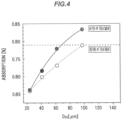
- absorption by the particulate single crystal phosphor obtained by pulverizing a single crystal phosphor ingot can be significantly improved by treating with hydrofluoric acid.
- FIG. 4 is a graph showing changes in absorption before and after treating a particulate single crystal phosphor (obtained by pulverizing a region of a single crystal phosphor ingot in which composition distribution is in a range from (Y 0.6462 Lu 0.3528 Ce 0.0010 ) 3.177 Al 4.823 O x to (Y 0.6870 Lu 0.3109 Ce 0.0021 ) 3.130 Al 4.870 O x ) with hydrofluoric acid.
- a surface of the particulate single crystal phosphor is etched with 40 % hydrofluoric acid at 40 °C for one hour.
- FIG. 4 shows that absorption by the particulate single crystal phosphor is significantly improved by the hydrofluoric acid treatment. Based on the fact that external quantum efficiency largely related to emission intensity of phosphor is indicated by a value obtained by multiplying internal quantum efficiency by absorption, it can be said that emission intensity of the particulate single crystal phosphor is significantly improved by the hydrofluoric acid treatment.
- FIGS. 5A and 5B are SEM (Scanning Electron Microscope) images showing the particulate single crystal phosphor respectively before and after hydrofluoric acid treatment.
- the single crystal phosphor after hydrofluoric acid treatment shown in FIG. 5B consists of particles each having rounded edges and has more curved surfaces than the single crystal phosphor before hydrofluoric acid treatment shown in FIG. 5A . It is considered that since the surfaces of the particles of the single crystal phosphor are curved as such, light reflection at the surface is reduced and absorption is improved. It is also considered that pulverizing has an effect of removing a crystal defect layer formed on the phosphor surface. Also, the rounded shape of the phosphor has such an effect that dispersibility when being dispersed in an inorganic sealing material is increased, the density of the phosphor in the film is improved, and thermal resistance is reduced.
- the second embodiment of the invention is a light-emitting device using the single crystal phosphor in the first embodiment.
- FIG. 6 is a schematic diagram illustrating a light source unit of a laser headlight 20 as a light-emitting device in the second embodiment.
- the laser headlight 20 has three laser diodes 22 each having a collimating lens 21, a condenser lens 23 for condensing blue laser light emitted from the laser diodes 22, a phosphor-including member 24 absorbing light condensed by the condenser lens 23 and emitting fluorescent light, and a mirror 25 reflecting the fluorescent light emitted from the phosphor-including member 24 and distributing light toward the front of the laser headlight 20.
- the laser headlight 20 is configured that white light is obtained by mixing blue light emitted from the laser diodes 22 and yellow light emitted from the phosphor-including member 24.
- FIGS. 7A and 7B are a cross sectional view and a plan view showing the phosphor-including member 24 in the second embodiment.
- the phosphor-including member 24 has a substrate 24a, a sealing material 24b formed on a surface of the substrate 24a, and a particulate phosphor 24c sealed in the sealing material 24b.
- the substrate 24a is a substrate having a highly reflective surface, such as mirror substrate. Also, the substrate 24a is preferably connected to a highly thermally conductive radiator formed of Cu or Al, etc.
- the planar shape of the substrate 24a is not specifically limited.
- the sealing material 24b is formed of a transparent inorganic material such as glass, SiO 2 -based or Al 2 O 3 -based material, and thus has excellent heat resistance as compared to a sealing material formed of an organic material such as silicone.
- the planar shape of the sealing material 24b may be a square as shown in FIG. 7B , or may be a circle as shown in FIG. 7C .
- the phosphor 24c is a phosphor formed of a particulate YAG-based or LuAG-based single crystal in the first embodiment, i.e., is a particulate phosphor which is formed of a single crystal having a composition represented by the compositional formula (Y 1-x-y-z Lu x Gd y Ce z ) 3+a Al 5-a O 12 ( 0 ⁇ x ⁇ 0.9994 , 0 ⁇ y ⁇ 0.0669 , 0.001 ⁇ z ⁇ 0.004 , -0.016 ⁇ a ⁇ 0.315) and has a particle diameter (D 50) of not less than 20 ⁇ m.
- the phosphor 24c is also a particulate phosphor group of which z in the compositional formula is, e.g., 0.001 ⁇ z ⁇ 0.004 and is continuously distributed between 0.001 and 0.004.
- the phosphor 24c has excellent emission properties under high-temperature conditions and can stably and efficiently emit fluorescent light even when the high-power laser diodes 22 are used as sources of excitation light.
- the third embodiment of the invention is a projector using the single crystal phosphor in the first embodiment.
- FIG. 8 is a schematic diagram illustrating a configuration of a projector 30 in the third embodiment.
- the projector 30 has a blue laser diode 31 as a light source, a phosphor-including member 33 which is excited by absorbing a portion of blue light emitted from the laser diode 31 and passing through a condenser lens 32 and emits yellow fluorescent light, a lens 34 for aligning the traveling direction of white light obtained by combining the yellow fluorescent light emitted from the phosphor-including member 33 and blue light transmitted without being absorbed by the phosphor-including member 33, a dichroic mirror 35a filtering white light passing through the lens 34 to allow for transmission of blue light and reflect the other light, a dichroic mirror 35b filtering the light reflected by the dichroic mirror 35a to allow for transmission of red light and reflect green light as the other light, a mirror 36a reflecting the blue light transmitted through the dichroic mirror 35a, mirrors 36b and 36c reflecting the red light transmitted through the dichroic mirror 35b,
- the lens 34, the dichroic mirrors 35a, 35b, the mirrors 36a, 36b, 36c, the liquid-crystal panels 37a, 37b, 37c and the prism 38 constitute an image-forming section which forms an image by processing fluorescent light emitted from the phosphor-including member 33 and light emitted from the laser diode 31 in the projector 30. That is, the projector 30 is configured that an image formed by the image-forming section using fluorescent light emitted from the phosphor-including member 33 is projected onto the external screen 100.
- FIGS. 9A and 9B are plan views showing the phosphor-including member 33 in the third embodiment.
- the phosphor-including member 33 has a disc-shaped transparent substrate 33a, an annular sealing material 33b formed on a surface of the transparent substrate 33a along the outer periphery thereof, and a particulate phosphor 33c sealed in the sealing material 33b.
- the transparent substrate 33a is formed of, e.g., sapphire having a high thermal conductivity and is placed inside the projector 30 so as to be rotatable in the circumferential direction.
- the sealing material 33b is formed of a transparent inorganic material such as glass, SiO 2 -based or Al 2 O 3 -based material, and thus has excellent heat resistance as compared to a sealing material formed of an organic material such as silicone.
- the phosphor 33c is a phosphor formed of a particulate YAG-based or LuAG-based single crystal in the first embodiment, i.e., is a particulate phosphor which is formed of a single crystal having a composition represented by the compositional formula (Y 1-x-y-z Lu x Gd y Ce z ) 3+a Al 5-a O 12 ( 0 ⁇ x ⁇ 0.9994 , 0 ⁇ y ⁇ 0.0669 , 0.001 ⁇ z ⁇ 0.004 , -0.016 ⁇ a ⁇ 0.315 ) and has a particle diameter (D 50 ) of not less than 20 ⁇ m.
- the phosphor 33c is also a particulate phosphor group of which z in the compositional formula is, e.g., 0.001 ⁇ z ⁇ 0.004 and is continuously distributed between 0.001 and 0.004.
- the phosphor 33c has excellent emission properties under high-temperature conditions and can stably and efficiently emit fluorescent light even when the high-power laser diode 31 is used as a source of excitation light.
- the phosphor 33c is excellent in emission properties at high temperature
- a phosphor-including member of stationary type can be used in some cases in place of the rotary type as is the phosphor-including member 33. It is difficult to use the known polycrystalline phosphors in such a way since thermal quenching occurs unless having excellent emission properties at high temperature.
- Such stationary phosphor-including member may be of transmissive type as is the phosphor-including member 33 using a transparent substrate, or may be of reflective type.
- the reflective phosphor-including member has, e.g., the same structure as the phosphor-including member 24 shown in FIG. 7 .
- a highly-reflective metal substrate such as Ag or Al substrate is preferably used as the substrate 24a.
- a surface of a metal substrate may be coated with a highly-reflective Ag- or Al-based material, etc.
- the light-emitting element used as a light source may be an LED in place of the laser diode 31.
- the effect by the phosphor-including member 33 i.e., excellent emission properties under high-temperature conditions, is exerted more significantly when using a high-power laser diode.
- the projector 30 is a projector having a configuration in which a spectrum of yellow emission from phosphor is dispersed into green spectrum and red spectrum
- the single crystal phosphor in the first embodiment can be used in a projector having a configuration in which green spectrum is directly extracted from a spectrum of green emission from phosphor.
- the single crystal phosphor in the first embodiment can be used regardless of the configuration of the image-forming section of the projector.
- a particulate phosphor which is formed of a YAG-based or LuAG-based single crystal and has excellent external quantum efficiency and excellent emission properties under high-temperature conditions. Also, by using such particulate phosphor, it is possible to manufacture light-emitting device and projector which are excellent in operating performance and reliability.
- Table 1 below is data from the single crystal phosphor ingot 16 grown by the CZ method and containing Lu in the Y site and shows a relation among distance from an interface with the seed crystal 15 in a direction parallel to the growth direction, value of z representing the Ce concentration in the compositional formula, CIE chromaticity coordinate x, and CIE chromaticity coordinate y.
- Table 1 Distance from Interface with Seed crystal [mm] Value of z CIE chromaticity coordinate x CIE chromaticity coordinate y 14.4 0.0009 0.397 0.573 28.8 Not measured 0.402 0.572 46.8 0.0012 0.404 0.571 66.0 Not measured 0.410 0.568 91.2 0.0070 0.436 0.549
- Table 1 shows that as the distance from the interface with the seed crystal 15 increases, the Ce concentration increases and the fluorescent color shifts from green to yellow.
- Example 2 Temperature dependence of emission properties of the phosphor-including member shown in FIG. 7A and 7B was examined in Example 2.
- Example 2 In the phosphor-including member in Example 2, an Al substrate was used as the substrate, a SiO x -based inorganic sealing material was used as the sealing material, and the particulate single crystal phosphor in the first embodiment having a particle diameter (D 50 ) of about 60 ⁇ m was used as the phosphor.
- D 50 particle diameter
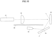
- FIG. 10 is a schematic diagram illustrating a configuration of a test optical system in Example 2.
- the test optical system has a blue laser diode array 41 as a light source, a phosphor-including member 43 which is excited by absorbing a portion of blue light emitted from the laser diode array 41 and passing through a condenser lens 42 and emits yellow fluorescent light, a dichroic mirror 44 filtering white light obtained by combining the yellow fluorescent light emitted from the phosphor-including member 43 and blue light reflected without being absorbed by the phosphor-including member 43 to allow for transmission of blue light and reflect yellow fluorescent light, a photodiode 45 receiving yellow light and generating photocurrent, and a light shielding plate 46 allowing the photodiode 45 to receive only the light reflected by the dichroic mirror 44.
- FIG. 11A is a graph showing a relation between output of the laser diode array 41 and surface temperature of phosphor sealed in three types of phosphor-including members 43 having different sealing-member thicknesses when the known YAG-based polycrystalline phosphor is used as the phosphor contained in the phosphor-including members 43.
- FIG. 11B is a graph showing a relation between output of the laser diode array 41 and fluorescence intensity of the three types of phosphor-including members 43 having different sealing-member thicknesses when the known YAG-based polycrystalline phosphor is used as the phosphor contained in the phosphor-including members 43.
- the particle diameter (D 50 ) of the known YAG-based polycrystalline phosphor pertaining to FIGS. 11A and 11B is 15 ⁇ m. Then, the thicknesses of the sealing materials of the three types of phosphor-including members 43 are 53 ⁇ m, 100 ⁇ m and 149 ⁇ m.
- FIG. 12A is a graph showing a relation between output of the laser diode array 41 and surface temperature of phosphor sealed in three types of phosphor-including members 43 having different sealing-member thicknesses when a YAG-based single crystal phosphor in the first embodiment (obtained by pulverizing a region of a single crystal phosphor ingot in which composition distribution is in a range of (Y 0.6462 Lu 0.3528 Ce 0.0010 ) 3.177 Al 4.823 O x from (Y 0.6870 Lu 0.3109 Ce 0.0021 ) 3.130 Al 4.870 O x ) is used as the phosphor contained in the phosphor-including members 43.
- FIG. 12B is a graph showing a relation between output of the laser diode array 41 and fluorescence intensity of the three types of phosphor-including members 43 having different sealing-member thicknesses when the YAG-based single crystal phosphor in the first embodiment (obtained by pulverizing a region from a single crystal phosphor ingot in which composition distribution is in a range of (Y 0.6462 Lu 0.3528 Ce 0.0010 ) 3.177 Al 4.823 O x to (Y 0.6870 Lu 0.3109 Ce 0.0021 ) 3.130 Al 4 . 870 O x ) is used as the phosphor contained in the phosphor-including members 43.
- the particle diameter (D 50) of the YAG-based single crystal phosphor pertaining to FIGS. 12A and 12B is 20 ⁇ m. Then, the thicknesses of the sealing materials of the three types of phosphor-including members 43 are 77 ⁇ m, 101 ⁇ m and 162 ⁇ m.
- the slope of the temperature increase of the known YAG-based polycrystalline phosphor becomes sharper with decreasing internal quantum efficiency when the surface temperature exceeds about 100 to 150 °C
- the slope of the temperature increase of the YAG-based single crystal phosphor in the first embodiment is substantially constant up to about 200 °C.
- the maximum value of fluorescence intensity of the known YAG-based polycrystalline phosphor was 29 when the thickness of the sealing material was 53 ⁇ m, but the maximum value of fluorescence intensity of the YAG-based single crystal phosphor in the first embodiment was 39 when the thickness of the sealing material was 101 ⁇ m, as shown in FIGS. 11B and 12B .
- Fluorescence intensity of the YAG-based single crystal phosphor in the first embodiment when the thickness of the sealing material was 77 ⁇ m, was not saturated even when output of the laser diode array 41 was increase to 78W, and it is expected that higher fluorescence intensity can be obtained.
- the invention is not intended to be limited to the embodiments and Examples, and the various kinds of modifications can be implemented without departing from the gist of the invention.
- a headlight has been described in the second embodiment as an example of the light-emitting device using the phosphor in the first embodiment and light-emitting elements, the light-emitting device is not limited thereto.
- a binder for binding particles of the phosphor may be used in place of the sealing material used to seal the particulate phosphor in the embodiments and Examples.
- the phosphor particles bound by the binder when used in a reflective phosphor-including member in the embodiments and Examples, are arranged on a substrate having a highly reflective surface, such as mirror substrate. Also, the phosphor particles bound by the binder has enough strength to self-stand. Therefore, the particles bonded into a plate shape can be used alone as a transmissive phosphor-including member, but may be arranged on a highly thermally conductive transparent substrate such as sapphire substrate to dissipate heat.
- the binder is formed of an inorganic material such as SiO 2 -based or Al 2 O 3 -based material.
- a particulate phosphor can be provided that includes a YAG-based or LuAG-based single crystal and that is excellent in external quantum efficiency and excellent in emission properties under high-temperature conditions, as well as a production method thereof, a phosphor-including member including the phosphor, and a light-emitting device or projector including the phosphor-including member.
Landscapes
- Chemical & Material Sciences (AREA)
- Organic Chemistry (AREA)
- Physics & Mathematics (AREA)
- Engineering & Computer Science (AREA)
- Materials Engineering (AREA)
- General Physics & Mathematics (AREA)
- Inorganic Chemistry (AREA)
- Metallurgy (AREA)
- Crystallography & Structural Chemistry (AREA)
- Optics & Photonics (AREA)
- Condensed Matter Physics & Semiconductors (AREA)
- Electromagnetism (AREA)
- Multimedia (AREA)
- Life Sciences & Earth Sciences (AREA)
- Geology (AREA)
- Luminescent Compositions (AREA)
- Projection Apparatus (AREA)
- Led Device Packages (AREA)
- Semiconductor Lasers (AREA)
Applications Claiming Priority (2)
| Application Number | Priority Date | Filing Date | Title |
|---|---|---|---|
| JP2016018448A JP6871665B2 (ja) | 2016-02-02 | 2016-02-02 | 蛍光体含有部材及びその製造方法、及び発光装置又はプロジェクター |
| PCT/JP2017/003793 WO2017135373A1 (ja) | 2016-02-02 | 2017-02-02 | 蛍光体及びその製造方法、蛍光体含有部材、及び発光装置又はプロジェクター |
Publications (3)
| Publication Number | Publication Date |
|---|---|
| EP3412752A1 EP3412752A1 (en) | 2018-12-12 |
| EP3412752A4 EP3412752A4 (en) | 2019-09-25 |
| EP3412752B1 true EP3412752B1 (en) | 2024-11-13 |
Family
ID=59500837
Family Applications (1)
| Application Number | Title | Priority Date | Filing Date |
|---|---|---|---|
| EP17747524.1A Active EP3412752B1 (en) | 2016-02-02 | 2017-02-02 | Phosphor-including member, and light emitting device or projector |
Country Status (5)
| Country | Link |
|---|---|
| US (1) | US11525082B2 (enExample) |
| EP (1) | EP3412752B1 (enExample) |
| JP (1) | JP6871665B2 (enExample) |
| CN (1) | CN108603113B (enExample) |
| WO (1) | WO2017135373A1 (enExample) |
Families Citing this family (6)
| Publication number | Priority date | Publication date | Assignee | Title |
|---|---|---|---|---|
| JP6917244B2 (ja) * | 2017-08-23 | 2021-08-11 | 日本特殊陶業株式会社 | 蛍光体ホイール、ホイールデバイスおよびプロジェクター |
| JP7224579B2 (ja) * | 2018-02-09 | 2023-02-20 | 株式会社タムラ製作所 | 波長変換部材 |
| JP7037082B2 (ja) * | 2019-09-27 | 2022-03-16 | 日亜化学工業株式会社 | 希土類アルミン酸塩蛍光体の製造方法、希土類アルミン酸塩蛍光体及び発光装置 |
| JP7429346B2 (ja) * | 2019-10-03 | 2024-02-08 | 国立研究開発法人物質・材料研究機構 | 波長変換部材 |
| US12467740B2 (en) | 2020-02-13 | 2025-11-11 | Hamamatsu Photonics K.K. | Imaging unit and measurement device |
| JP2022039095A (ja) | 2020-08-27 | 2022-03-10 | セイコーエプソン株式会社 | 蛍光体粒子、波長変換素子、光源装置、蛍光体粒子の製造方法、波長変換素子の製造方法、及びプロジェクター |
Family Cites Families (11)
| Publication number | Priority date | Publication date | Assignee | Title |
|---|---|---|---|---|
| JPS5620562B2 (enExample) | 1972-12-04 | 1981-05-14 | ||
| JPH09291279A (ja) * | 1996-04-25 | 1997-11-11 | Noritake Co Ltd | 粉末蛍光体およびその製造方法 |
| CN1560332A (zh) * | 2004-02-23 | 2005-01-05 | 中国科学院上海光学精密机械研究所 | 掺三价铈离子的钇铝石榴石闪烁晶体的制备方法 |
| JP4583076B2 (ja) | 2004-06-11 | 2010-11-17 | スタンレー電気株式会社 | 発光素子 |
| WO2013161683A1 (ja) | 2012-04-24 | 2013-10-31 | 株式会社光波 | 蛍光体及びその製造方法、並びに発光装置 |
| JP5620562B1 (ja) | 2013-10-23 | 2014-11-05 | 株式会社光波 | 単結晶蛍光体及び発光装置 |
| JP6384893B2 (ja) | 2013-10-23 | 2018-09-05 | 株式会社光波 | 単結晶蛍光体及び発光装置 |
| CN103820859A (zh) * | 2013-12-31 | 2014-05-28 | 西南技术物理研究所 | 掺杂钇铝石榴石陶瓷转变为单晶的制备方法 |
| DE112016003272T5 (de) * | 2015-07-22 | 2018-04-05 | Panasonic Intellectual Property Management Co., Ltd. | Granatverbindung und Verfahren zu deren Herstellung, lichtemittierende Vorrichtung und Dekorgegenstand, bei denen die Granatverbindung verwendet wird, und Verfahren zur Verwendung der Granatverbindung |
| JP2017120864A (ja) * | 2015-12-28 | 2017-07-06 | 株式会社タムラ製作所 | 発光装置 |
| KR102675945B1 (ko) * | 2018-09-18 | 2024-06-17 | 삼성전자주식회사 | 발광 장치 |
-
2016
- 2016-02-02 JP JP2016018448A patent/JP6871665B2/ja active Active
-
2017
- 2017-02-02 CN CN201780009385.XA patent/CN108603113B/zh active Active
- 2017-02-02 WO PCT/JP2017/003793 patent/WO2017135373A1/ja not_active Ceased
- 2017-02-02 US US16/074,163 patent/US11525082B2/en active Active
- 2017-02-02 EP EP17747524.1A patent/EP3412752B1/en active Active
Also Published As
| Publication number | Publication date |
|---|---|
| JP6871665B2 (ja) | 2021-05-12 |
| US20210122975A1 (en) | 2021-04-29 |
| JP2017137394A (ja) | 2017-08-10 |
| EP3412752A1 (en) | 2018-12-12 |
| US11525082B2 (en) | 2022-12-13 |
| CN108603113A (zh) | 2018-09-28 |
| WO2017135373A1 (ja) | 2017-08-10 |
| CN108603113B (zh) | 2022-07-05 |
| EP3412752A4 (en) | 2019-09-25 |
Similar Documents
| Publication | Publication Date | Title |
|---|---|---|
| EP3412752B1 (en) | Phosphor-including member, and light emitting device or projector | |
| EP3438229B1 (en) | Fluorescent body, light-emitting device, illuminating apparatus, and image display apparatus | |
| KR102144151B1 (ko) | 단결정 형광체 | |
| Park et al. | High power and temperature luminescence of Y3Al5O12: Ce3+ bulky and pulverized single crystal phosphors by a floating-zone method | |
| KR101812997B1 (ko) | 실리케이트 형광체, 실리케이트 형광체의 제조방법 및 이를 포함하는 발광 장치 | |
| TWI515284B (zh) | 螢光體粒子,其製造方法,及發光二極體 | |
| TWI428309B (zh) | A ceramic composite for optical conversion and a light-emitting device using the ceramic composite | |
| TWI535824B (zh) | A ceramic composite for optical conversion and a light-emitting device using the same | |
| TWI500591B (zh) | A ceramic composite for optical conversion, a method for manufacturing the same, and a light-emitting device provided with the same | |
| JP7178074B2 (ja) | 波長変換部材及び波長変換素子、並びに波長変換部材の製造方法 | |
| Wang et al. | Molten-salt synthesis of large micron-sized YAG: Ce3+ phosphors for laser diode applications | |
| CN112310264A (zh) | 发光装置及其制造方法 | |
| US12365837B2 (en) | Wavelength conversion member | |
| US10174245B2 (en) | Method for producing a luminescent material, luminescent material and optoelectronic component | |
| WO2025121388A1 (ja) | 蛍光体、発光装置、照明装置、画像表示装置及び車両用表示灯 | |
| WO2019156159A1 (ja) | 波長変換部材 |
Legal Events
| Date | Code | Title | Description |
|---|---|---|---|
| STAA | Information on the status of an ep patent application or granted ep patent |
Free format text: STATUS: THE INTERNATIONAL PUBLICATION HAS BEEN MADE |
|
| PUAI | Public reference made under article 153(3) epc to a published international application that has entered the european phase |
Free format text: ORIGINAL CODE: 0009012 |
|
| STAA | Information on the status of an ep patent application or granted ep patent |
Free format text: STATUS: REQUEST FOR EXAMINATION WAS MADE |
|
| 17P | Request for examination filed |
Effective date: 20180903 |
|
| AK | Designated contracting states |
Kind code of ref document: A1 Designated state(s): AL AT BE BG CH CY CZ DE DK EE ES FI FR GB GR HR HU IE IS IT LI LT LU LV MC MK MT NL NO PL PT RO RS SE SI SK SM TR |
|
| AX | Request for extension of the european patent |
Extension state: BA ME |
|
| DAV | Request for validation of the european patent (deleted) | ||
| DAX | Request for extension of the european patent (deleted) | ||
| A4 | Supplementary search report drawn up and despatched |
Effective date: 20190826 |
|
| RIC1 | Information provided on ipc code assigned before grant |
Ipc: H01S 5/022 20060101ALI20190820BHEP Ipc: G03B 21/14 20060101ALI20190820BHEP Ipc: C09K 11/77 20060101ALI20190820BHEP Ipc: C09K 11/80 20060101AFI20190820BHEP Ipc: G03B 21/00 20060101ALI20190820BHEP |
|
| STAA | Information on the status of an ep patent application or granted ep patent |
Free format text: STATUS: EXAMINATION IS IN PROGRESS |
|
| 17Q | First examination report despatched |
Effective date: 20200722 |
|
| RAP1 | Party data changed (applicant data changed or rights of an application transferred) |
Owner name: NATIONAL INSTITUTE FOR MATERIALS SCIENCE Owner name: TAMURA CORPORATION |
|
| RAP1 | Party data changed (applicant data changed or rights of an application transferred) |
Owner name: NATIONAL INSTITUTE FOR MATERIALS SCIENCE |
|
| GRAP | Despatch of communication of intention to grant a patent |
Free format text: ORIGINAL CODE: EPIDOSNIGR1 |
|
| STAA | Information on the status of an ep patent application or granted ep patent |
Free format text: STATUS: GRANT OF PATENT IS INTENDED |
|
| INTG | Intention to grant announced |
Effective date: 20231204 |
|
| GRAJ | Information related to disapproval of communication of intention to grant by the applicant or resumption of examination proceedings by the epo deleted |
Free format text: ORIGINAL CODE: EPIDOSDIGR1 |
|
| STAA | Information on the status of an ep patent application or granted ep patent |
Free format text: STATUS: EXAMINATION IS IN PROGRESS |
|
| INTC | Intention to grant announced (deleted) | ||
| GRAP | Despatch of communication of intention to grant a patent |
Free format text: ORIGINAL CODE: EPIDOSNIGR1 |
|
| STAA | Information on the status of an ep patent application or granted ep patent |
Free format text: STATUS: GRANT OF PATENT IS INTENDED |
|
| INTG | Intention to grant announced |
Effective date: 20240603 |
|
| GRAS | Grant fee paid |
Free format text: ORIGINAL CODE: EPIDOSNIGR3 |
|
| GRAA | (expected) grant |
Free format text: ORIGINAL CODE: 0009210 |
|
| STAA | Information on the status of an ep patent application or granted ep patent |
Free format text: STATUS: THE PATENT HAS BEEN GRANTED |
|
| AK | Designated contracting states |
Kind code of ref document: B1 Designated state(s): AL AT BE BG CH CY CZ DE DK EE ES FI FR GB GR HR HU IE IS IT LI LT LU LV MC MK MT NL NO PL PT RO RS SE SI SK SM TR |
|
| REG | Reference to a national code |
Ref country code: GB Ref legal event code: FG4D |
|
| REG | Reference to a national code |
Ref country code: CH Ref legal event code: EP |
|
| REG | Reference to a national code |
Ref country code: DE Ref legal event code: R096 Ref document number: 602017086100 Country of ref document: DE |
|
| REG | Reference to a national code |
Ref country code: IE Ref legal event code: FG4D |
|
| REG | Reference to a national code |
Ref country code: LT Ref legal event code: MG9D |
|
| REG | Reference to a national code |
Ref country code: NL Ref legal event code: MP Effective date: 20241113 |
|
| PG25 | Lapsed in a contracting state [announced via postgrant information from national office to epo] |
Ref country code: PT Free format text: LAPSE BECAUSE OF FAILURE TO SUBMIT A TRANSLATION OF THE DESCRIPTION OR TO PAY THE FEE WITHIN THE PRESCRIBED TIME-LIMIT Effective date: 20250313 Ref country code: HR Free format text: LAPSE BECAUSE OF FAILURE TO SUBMIT A TRANSLATION OF THE DESCRIPTION OR TO PAY THE FEE WITHIN THE PRESCRIBED TIME-LIMIT Effective date: 20241113 Ref country code: IS Free format text: LAPSE BECAUSE OF FAILURE TO SUBMIT A TRANSLATION OF THE DESCRIPTION OR TO PAY THE FEE WITHIN THE PRESCRIBED TIME-LIMIT Effective date: 20250313 |
|
| PG25 | Lapsed in a contracting state [announced via postgrant information from national office to epo] |
Ref country code: FI Free format text: LAPSE BECAUSE OF FAILURE TO SUBMIT A TRANSLATION OF THE DESCRIPTION OR TO PAY THE FEE WITHIN THE PRESCRIBED TIME-LIMIT Effective date: 20241113 Ref country code: NL Free format text: LAPSE BECAUSE OF FAILURE TO SUBMIT A TRANSLATION OF THE DESCRIPTION OR TO PAY THE FEE WITHIN THE PRESCRIBED TIME-LIMIT Effective date: 20241113 |
|
| REG | Reference to a national code |
Ref country code: AT Ref legal event code: MK05 Ref document number: 1741699 Country of ref document: AT Kind code of ref document: T Effective date: 20241113 |
|
| PG25 | Lapsed in a contracting state [announced via postgrant information from national office to epo] |
Ref country code: BG Free format text: LAPSE BECAUSE OF FAILURE TO SUBMIT A TRANSLATION OF THE DESCRIPTION OR TO PAY THE FEE WITHIN THE PRESCRIBED TIME-LIMIT Effective date: 20241113 |
|
| PG25 | Lapsed in a contracting state [announced via postgrant information from national office to epo] |
Ref country code: ES Free format text: LAPSE BECAUSE OF FAILURE TO SUBMIT A TRANSLATION OF THE DESCRIPTION OR TO PAY THE FEE WITHIN THE PRESCRIBED TIME-LIMIT Effective date: 20241113 |
|
| PG25 | Lapsed in a contracting state [announced via postgrant information from national office to epo] |
Ref country code: NO Free format text: LAPSE BECAUSE OF FAILURE TO SUBMIT A TRANSLATION OF THE DESCRIPTION OR TO PAY THE FEE WITHIN THE PRESCRIBED TIME-LIMIT Effective date: 20250213 |
|
| PG25 | Lapsed in a contracting state [announced via postgrant information from national office to epo] |
Ref country code: GR Free format text: LAPSE BECAUSE OF FAILURE TO SUBMIT A TRANSLATION OF THE DESCRIPTION OR TO PAY THE FEE WITHIN THE PRESCRIBED TIME-LIMIT Effective date: 20250214 Ref country code: LV Free format text: LAPSE BECAUSE OF FAILURE TO SUBMIT A TRANSLATION OF THE DESCRIPTION OR TO PAY THE FEE WITHIN THE PRESCRIBED TIME-LIMIT Effective date: 20241113 Ref country code: AT Free format text: LAPSE BECAUSE OF FAILURE TO SUBMIT A TRANSLATION OF THE DESCRIPTION OR TO PAY THE FEE WITHIN THE PRESCRIBED TIME-LIMIT Effective date: 20241113 |
|
| PG25 | Lapsed in a contracting state [announced via postgrant information from national office to epo] |
Ref country code: PL Free format text: LAPSE BECAUSE OF FAILURE TO SUBMIT A TRANSLATION OF THE DESCRIPTION OR TO PAY THE FEE WITHIN THE PRESCRIBED TIME-LIMIT Effective date: 20241113 |
|
| PG25 | Lapsed in a contracting state [announced via postgrant information from national office to epo] |
Ref country code: RS Free format text: LAPSE BECAUSE OF FAILURE TO SUBMIT A TRANSLATION OF THE DESCRIPTION OR TO PAY THE FEE WITHIN THE PRESCRIBED TIME-LIMIT Effective date: 20250213 |
|
| PG25 | Lapsed in a contracting state [announced via postgrant information from national office to epo] |
Ref country code: SM Free format text: LAPSE BECAUSE OF FAILURE TO SUBMIT A TRANSLATION OF THE DESCRIPTION OR TO PAY THE FEE WITHIN THE PRESCRIBED TIME-LIMIT Effective date: 20241113 |
|
| PG25 | Lapsed in a contracting state [announced via postgrant information from national office to epo] |
Ref country code: DK Free format text: LAPSE BECAUSE OF FAILURE TO SUBMIT A TRANSLATION OF THE DESCRIPTION OR TO PAY THE FEE WITHIN THE PRESCRIBED TIME-LIMIT Effective date: 20241113 |
|
| PG25 | Lapsed in a contracting state [announced via postgrant information from national office to epo] |
Ref country code: EE Free format text: LAPSE BECAUSE OF FAILURE TO SUBMIT A TRANSLATION OF THE DESCRIPTION OR TO PAY THE FEE WITHIN THE PRESCRIBED TIME-LIMIT Effective date: 20241113 |
|
| PG25 | Lapsed in a contracting state [announced via postgrant information from national office to epo] |
Ref country code: RO Free format text: LAPSE BECAUSE OF FAILURE TO SUBMIT A TRANSLATION OF THE DESCRIPTION OR TO PAY THE FEE WITHIN THE PRESCRIBED TIME-LIMIT Effective date: 20241113 |
|
| PG25 | Lapsed in a contracting state [announced via postgrant information from national office to epo] |
Ref country code: SK Free format text: LAPSE BECAUSE OF FAILURE TO SUBMIT A TRANSLATION OF THE DESCRIPTION OR TO PAY THE FEE WITHIN THE PRESCRIBED TIME-LIMIT Effective date: 20241113 |
|
| PG25 | Lapsed in a contracting state [announced via postgrant information from national office to epo] |
Ref country code: CZ Free format text: LAPSE BECAUSE OF FAILURE TO SUBMIT A TRANSLATION OF THE DESCRIPTION OR TO PAY THE FEE WITHIN THE PRESCRIBED TIME-LIMIT Effective date: 20241113 |
|
| PG25 | Lapsed in a contracting state [announced via postgrant information from national office to epo] |
Ref country code: IT Free format text: LAPSE BECAUSE OF FAILURE TO SUBMIT A TRANSLATION OF THE DESCRIPTION OR TO PAY THE FEE WITHIN THE PRESCRIBED TIME-LIMIT Effective date: 20241113 |
|
| REG | Reference to a national code |
Ref country code: DE Ref legal event code: R097 Ref document number: 602017086100 Country of ref document: DE |
|
| PG25 | Lapsed in a contracting state [announced via postgrant information from national office to epo] |
Ref country code: SE Free format text: LAPSE BECAUSE OF FAILURE TO SUBMIT A TRANSLATION OF THE DESCRIPTION OR TO PAY THE FEE WITHIN THE PRESCRIBED TIME-LIMIT Effective date: 20241113 |
|
| PG25 | Lapsed in a contracting state [announced via postgrant information from national office to epo] |
Ref country code: MC Free format text: LAPSE BECAUSE OF FAILURE TO SUBMIT A TRANSLATION OF THE DESCRIPTION OR TO PAY THE FEE WITHIN THE PRESCRIBED TIME-LIMIT Effective date: 20241113 |
|
| PLBE | No opposition filed within time limit |
Free format text: ORIGINAL CODE: 0009261 |
|
| STAA | Information on the status of an ep patent application or granted ep patent |
Free format text: STATUS: NO OPPOSITION FILED WITHIN TIME LIMIT |
|
| REG | Reference to a national code |
Ref country code: CH Ref legal event code: PL |
|
| PG25 | Lapsed in a contracting state [announced via postgrant information from national office to epo] |
Ref country code: LU Free format text: LAPSE BECAUSE OF NON-PAYMENT OF DUE FEES Effective date: 20250202 |
|
| PG25 | Lapsed in a contracting state [announced via postgrant information from national office to epo] |
Ref country code: CH Free format text: LAPSE BECAUSE OF NON-PAYMENT OF DUE FEES Effective date: 20250228 |
|
| 26N | No opposition filed |
Effective date: 20250814 |
|
| GBPC | Gb: european patent ceased through non-payment of renewal fee |
Effective date: 20250213 |
|
| REG | Reference to a national code |
Ref country code: BE Ref legal event code: MM Effective date: 20250228 |
|
| PG25 | Lapsed in a contracting state [announced via postgrant information from national office to epo] |
Ref country code: GB Free format text: LAPSE BECAUSE OF NON-PAYMENT OF DUE FEES Effective date: 20250213 |
|
| PG25 | Lapsed in a contracting state [announced via postgrant information from national office to epo] |
Ref country code: BE Free format text: LAPSE BECAUSE OF NON-PAYMENT OF DUE FEES Effective date: 20250228 |
|
| PG25 | Lapsed in a contracting state [announced via postgrant information from national office to epo] |
Ref country code: IE Free format text: LAPSE BECAUSE OF NON-PAYMENT OF DUE FEES Effective date: 20250202 |
|
| PGFP | Annual fee paid to national office [announced via postgrant information from national office to epo] |
Ref country code: DE Payment date: 20260218 Year of fee payment: 10 |
|
| PGFP | Annual fee paid to national office [announced via postgrant information from national office to epo] |
Ref country code: FR Payment date: 20260218 Year of fee payment: 10 |