EP3389086B1 - Verfahren zur herstellung einer verbundschicht und werkstück mit einer verbundschicht - Google Patents
Verfahren zur herstellung einer verbundschicht und werkstück mit einer verbundschicht Download PDFInfo
- Publication number
- EP3389086B1 EP3389086B1 EP18166919.3A EP18166919A EP3389086B1 EP 3389086 B1 EP3389086 B1 EP 3389086B1 EP 18166919 A EP18166919 A EP 18166919A EP 3389086 B1 EP3389086 B1 EP 3389086B1
- Authority
- EP
- European Patent Office
- Prior art keywords
- heat sink
- depositing
- layer
- thermally conductive
- semiconductor package
- Prior art date
- Legal status (The legal status is an assumption and is not a legal conclusion. Google has not performed a legal analysis and makes no representation as to the accuracy of the status listed.)
- Active
Links
Images














Classifications
-
- B—PERFORMING OPERATIONS; TRANSPORTING
- B29—WORKING OF PLASTICS; WORKING OF SUBSTANCES IN A PLASTIC STATE IN GENERAL
- B29C—SHAPING OR JOINING OF PLASTICS; SHAPING OF MATERIAL IN A PLASTIC STATE, NOT OTHERWISE PROVIDED FOR; AFTER-TREATMENT OF THE SHAPED PRODUCTS, e.g. REPAIRING
- B29C70/00—Shaping composites, i.e. plastics material comprising reinforcements, fillers or preformed parts, e.g. inserts
- B29C70/58—Shaping composites, i.e. plastics material comprising reinforcements, fillers or preformed parts, e.g. inserts comprising fillers only, e.g. particles, powder, beads, flakes, spheres
-
- H—ELECTRICITY
- H10—SEMICONDUCTOR DEVICES; ELECTRIC SOLID-STATE DEVICES NOT OTHERWISE PROVIDED FOR
- H10W—GENERIC PACKAGES, INTERCONNECTIONS, CONNECTORS OR OTHER CONSTRUCTIONAL DETAILS OF DEVICES COVERED BY CLASS H10
- H10W95/00—Packaging processes not covered by the other groups of this subclass
-
- B—PERFORMING OPERATIONS; TRANSPORTING
- B29—WORKING OF PLASTICS; WORKING OF SUBSTANCES IN A PLASTIC STATE IN GENERAL
- B29C—SHAPING OR JOINING OF PLASTICS; SHAPING OF MATERIAL IN A PLASTIC STATE, NOT OTHERWISE PROVIDED FOR; AFTER-TREATMENT OF THE SHAPED PRODUCTS, e.g. REPAIRING
- B29C70/00—Shaping composites, i.e. plastics material comprising reinforcements, fillers or preformed parts, e.g. inserts
- B29C70/68—Shaping composites, i.e. plastics material comprising reinforcements, fillers or preformed parts, e.g. inserts by incorporating or moulding on preformed parts, e.g. inserts or layers, e.g. foam blocks
- B29C70/78—Moulding material on one side only of the preformed part
-
- H—ELECTRICITY
- H10—SEMICONDUCTOR DEVICES; ELECTRIC SOLID-STATE DEVICES NOT OTHERWISE PROVIDED FOR
- H10W—GENERIC PACKAGES, INTERCONNECTIONS, CONNECTORS OR OTHER CONSTRUCTIONAL DETAILS OF DEVICES COVERED BY CLASS H10
- H10W40/00—Arrangements for thermal protection or thermal control
- H10W40/20—Arrangements for cooling
- H10W40/25—Arrangements for cooling characterised by their materials
-
- H—ELECTRICITY
- H10—SEMICONDUCTOR DEVICES; ELECTRIC SOLID-STATE DEVICES NOT OTHERWISE PROVIDED FOR
- H10W—GENERIC PACKAGES, INTERCONNECTIONS, CONNECTORS OR OTHER CONSTRUCTIONAL DETAILS OF DEVICES COVERED BY CLASS H10
- H10W40/00—Arrangements for thermal protection or thermal control
- H10W40/20—Arrangements for cooling
- H10W40/25—Arrangements for cooling characterised by their materials
- H10W40/251—Organics
-
- H—ELECTRICITY
- H10—SEMICONDUCTOR DEVICES; ELECTRIC SOLID-STATE DEVICES NOT OTHERWISE PROVIDED FOR
- H10W—GENERIC PACKAGES, INTERCONNECTIONS, CONNECTORS OR OTHER CONSTRUCTIONAL DETAILS OF DEVICES COVERED BY CLASS H10
- H10W40/00—Arrangements for thermal protection or thermal control
- H10W40/20—Arrangements for cooling
- H10W40/25—Arrangements for cooling characterised by their materials
- H10W40/257—Arrangements for cooling characterised by their materials having a heterogeneous or anisotropic structure, e.g. powder or fibres in a matrix, wire mesh or porous structures
-
- H—ELECTRICITY
- H10—SEMICONDUCTOR DEVICES; ELECTRIC SOLID-STATE DEVICES NOT OTHERWISE PROVIDED FOR
- H10W—GENERIC PACKAGES, INTERCONNECTIONS, CONNECTORS OR OTHER CONSTRUCTIONAL DETAILS OF DEVICES COVERED BY CLASS H10
- H10W40/00—Arrangements for thermal protection or thermal control
- H10W40/70—Fillings or auxiliary members in containers or in encapsulations for thermal protection or control
-
- H—ELECTRICITY
- H10—SEMICONDUCTOR DEVICES; ELECTRIC SOLID-STATE DEVICES NOT OTHERWISE PROVIDED FOR
- H10W—GENERIC PACKAGES, INTERCONNECTIONS, CONNECTORS OR OTHER CONSTRUCTIONAL DETAILS OF DEVICES COVERED BY CLASS H10
- H10W40/00—Arrangements for thermal protection or thermal control
- H10W40/70—Fillings or auxiliary members in containers or in encapsulations for thermal protection or control
- H10W40/77—Auxiliary members characterised by their shape
-
- H—ELECTRICITY
- H10—SEMICONDUCTOR DEVICES; ELECTRIC SOLID-STATE DEVICES NOT OTHERWISE PROVIDED FOR
- H10W—GENERIC PACKAGES, INTERCONNECTIONS, CONNECTORS OR OTHER CONSTRUCTIONAL DETAILS OF DEVICES COVERED BY CLASS H10
- H10W70/00—Package substrates; Interposers; Redistribution layers [RDL]
- H10W70/01—Manufacture or treatment
- H10W70/02—Manufacture or treatment of conductive package substrates serving as an interconnection, e.g. of metal plates
-
- H—ELECTRICITY
- H10—SEMICONDUCTOR DEVICES; ELECTRIC SOLID-STATE DEVICES NOT OTHERWISE PROVIDED FOR
- H10W—GENERIC PACKAGES, INTERCONNECTIONS, CONNECTORS OR OTHER CONSTRUCTIONAL DETAILS OF DEVICES COVERED BY CLASS H10
- H10W70/00—Package substrates; Interposers; Redistribution layers [RDL]
- H10W70/40—Leadframes
- H10W70/461—Leadframes specially adapted for cooling
-
- H—ELECTRICITY
- H10—SEMICONDUCTOR DEVICES; ELECTRIC SOLID-STATE DEVICES NOT OTHERWISE PROVIDED FOR
- H10W—GENERIC PACKAGES, INTERCONNECTIONS, CONNECTORS OR OTHER CONSTRUCTIONAL DETAILS OF DEVICES COVERED BY CLASS H10
- H10W99/00—Subject matter not provided for in other groups of this subclass
-
- B—PERFORMING OPERATIONS; TRANSPORTING
- B29—WORKING OF PLASTICS; WORKING OF SUBSTANCES IN A PLASTIC STATE IN GENERAL
- B29K—INDEXING SCHEME ASSOCIATED WITH SUBCLASSES B29B, B29C OR B29D, RELATING TO MOULDING MATERIALS OR TO MATERIALS FOR MOULDS, REINFORCEMENTS, FILLERS OR PREFORMED PARTS, e.g. INSERTS
- B29K2509/00—Use of inorganic materials not provided for in groups B29K2503/00 - B29K2507/00, as filler
- B29K2509/02—Ceramics
- B29K2509/04—Carbides; Nitrides
-
- B—PERFORMING OPERATIONS; TRANSPORTING
- B29—WORKING OF PLASTICS; WORKING OF SUBSTANCES IN A PLASTIC STATE IN GENERAL
- B29L—INDEXING SCHEME ASSOCIATED WITH SUBCLASS B29C, RELATING TO PARTICULAR ARTICLES
- B29L2031/00—Other particular articles
- B29L2031/34—Electrical apparatus, e.g. sparking plugs or parts thereof
-
- H—ELECTRICITY
- H10—SEMICONDUCTOR DEVICES; ELECTRIC SOLID-STATE DEVICES NOT OTHERWISE PROVIDED FOR
- H10W—GENERIC PACKAGES, INTERCONNECTIONS, CONNECTORS OR OTHER CONSTRUCTIONAL DETAILS OF DEVICES COVERED BY CLASS H10
- H10W40/00—Arrangements for thermal protection or thermal control
- H10W40/20—Arrangements for cooling
- H10W40/22—Arrangements for cooling characterised by their shape, e.g. having conical or cylindrical projections
-
- H—ELECTRICITY
- H10—SEMICONDUCTOR DEVICES; ELECTRIC SOLID-STATE DEVICES NOT OTHERWISE PROVIDED FOR
- H10W—GENERIC PACKAGES, INTERCONNECTIONS, CONNECTORS OR OTHER CONSTRUCTIONAL DETAILS OF DEVICES COVERED BY CLASS H10
- H10W40/00—Arrangements for thermal protection or thermal control
- H10W40/70—Fillings or auxiliary members in containers or in encapsulations for thermal protection or control
- H10W40/77—Auxiliary members characterised by their shape
- H10W40/778—Auxiliary members characterised by their shape in encapsulations
-
- H—ELECTRICITY
- H10—SEMICONDUCTOR DEVICES; ELECTRIC SOLID-STATE DEVICES NOT OTHERWISE PROVIDED FOR
- H10W—GENERIC PACKAGES, INTERCONNECTIONS, CONNECTORS OR OTHER CONSTRUCTIONAL DETAILS OF DEVICES COVERED BY CLASS H10
- H10W74/00—Encapsulations, e.g. protective coatings
Definitions
- This disclosure in general relates to a semiconductor component and a method for producing a semiconductor component, in particular a semiconductor component comprising means for attaching the semiconductor component to a heat sink.
- Semiconductor components are usually packaged and then mounted to a printed circuit board.
- the semiconductor components may further be coupled to a heat sink, wherein the heat sink is configured to dissipate heat produced by the semiconductor component.
- a heat sink is configured to dissipate heat produced by the semiconductor component.
- Such mounting methods are often expensive, require a lot of space, and require one or more additional process steps for mounting the component to the heat sink.
- Document US 2014/192500 A1 discloses a system comprising a component carrier, a component disposed on the component carrier and an insulating layer disposed on an electrically conductive surface of at least one of the component carrier or the component, wherein the insulating layer comprises a polymer and an inorganic material comprising a dielectric strength of equal or greater than 15 ac-kv/mm and a thermal conductivity of equal or greater than 15 W/m*K.
- the method includes forming a first thermally conductive layer on an outer surface of a semiconductor package.
- Forming the first thermally conductive layer comprises depositing a first material on the outer surface of the semiconductor package, and depositing a second material on the first material after depositing the first material.
- the first material comprises at least one of boron nitride, aluminium oxide, silicon carbide, silicon dioxide, or a ceramic material including an oxide or nitride combination.
- the first thermally conductive layer formed on the outer surface of the semiconductor package is configured to be mounted to an external heat sink.
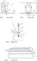
- FIG. 1 shows one known possibility for attaching a semiconductor component 100 to a heat sink 111.
- the semiconductor component 100 comprises a package 110.
- One or more semiconductor dies may be arranged within the semiconductor package 110.
- the package 110 may comprise one or more pins or leads 113 for mounting the semiconductor component 100 to a printed circuit board 200 and for providing an electrical connection between the semiconductor die(s) in the package 110 and the surrounding circuitry (e.g., on the printed circuit board 200).
- the semiconductor component 100 is further coupled to a heat sink 111.
- isolation foil 112 is arranged between the semiconductor component 100 and the heat sink 111.
- the isolation foil 112 is configured to dissipate heat from the semiconductor component 100 to the heat sink 111.
- the use of isolation foils 112, however, is usually rather expensive.
- a further drawback of isolation foils 112 is that additional process steps are required. This is because the semiconductor component 100, the heat sink 111 and the isolation foil 112 have to be purchased separately and subsequently have to be assembled by an end user.
- the isolation foil 112 is first laminated to the heat sink 111 and then the semiconductor component 100 is attached to the isolation foil 112.
- the isolation foil 112 may be a ceramic foil, for example.
- the isolation foil 112 generally may be electrically non-conductive and thermally conductive.
- FIG 3 illustrates another example of a known method for mounting a semiconductor component 100 to a heat sink 111.
- the heat sink 111 and the semiconductor component 100 each comprise a hole 121, 122.
- a screw 120 may be inserted into the holes 121, 122 to fix the semiconductor component 100 to the heat sink 111.
- a compression washer 123 may be inserted between the screw 120 and the semiconductor component 100.
- This method also has several drawbacks.
- the thermal conductivity depends on a filler material (usually Silicon) that acts as a thermal dissipator and the resulting Silicon/Resin ratio is usually limited/balanced by the moldability performance.
- Other mechanical fasteners are known for attaching a semiconductor component 100 to a heat sink 111, including nuts and bolts or spring clips with either greased mica or thermally-enhanced silicone pads, for example.
- the semiconductor component 100 is mounted on a substrate 130, in particular a direct copper bonded (DCB) substrate 130.
- the DCB substrate comprises a ceramic dielectric insulator layer 131. Pure copper layers 132 are applied and bonded to the ceramic layer 131 on both sides using great adhesive strength in a high temperature melting and diffusion process.
- the semiconductor component 100 is then soldered to a first side of the DCB substrate 130 using a solder layer 135.
- the heat sink 111 may be coupled to the second side of the DCB substrate 130 opposite the first surface.
- a heat spreader 136 may be inserted between the DCB substrate 130 and the heat sink 111.
- the DCB substrate 130 may be soldered to the heat spreader 136 by means of a solder layer 135.
- a thermal grease layer 137 may be arranged between the heat spreader 136 and the heat sink 111.
- the heat spreader 136 may be a copper baseplate or aluminium baseplate. However, especially in the lower power range, arrangements without a baseplate are also frequently used. In such an arrangement the second solder layer 135 and heat spreader 136 may be omitted and the DCB substrate 130 may be coupled to the heat sink 111 via the thermal grease layer 137. Even though an arrangement including a DCB substrate 130 has several advantages such as a high mechanical strength and mechanical stability, good adhesion and corrosion resistance, and a very good thermal conductivity, it also has some drawbacks. The drawbacks include high costs. Furthermore, several additional process steps are required during assembly of the arrangement and the isolation is rather thick (e.g., minimum of 250 ⁇ m).
- FIG. 5 illustrates a semiconductor component 100 which is not part of the claimed invention.
- the semiconductor component 100 comprises a semiconductor package 110.
- a first thermally conductive layer 115 is arranged on an outer surface of the semiconductor package 110.
- the first thermally conductive layer 115 formed on the outer surface of the semiconductor package is configured to be mounted to an external heat sink 111.
- the semiconductor component 100 with the first thermally conductive layer 115 arranged on the outer surface of the semiconductor component 110 is configured to be mounted to an external heat sink 111 such that the first thermally conductive layer 115 faces the heat sink 111.
- a method for producing a semiconductor component 100 comprises forming a first thermally conductive layer 115 on an outer surface of a semiconductor package 110.
- the first thermally conductive layer 115 formed on the outer surface of the semiconductor package 110 is configured to be mounted to an external heat sink 111.
- the semiconductor component 100 includes at least one semiconductor die 114 (see Figure 11 ) that is arranged within the semiconductor package 110.
- the first thermally conductive layer 115 may be arranged on a first outer surface or external surface of the semiconductor package 110.
- the first outer surface of the semiconductor package 110 may comprise an electrically conductive surface 140 such as a heat sink or exposed die pad (see Figure 11 ), for example.
- the electrically conductive surface 140 may comprise an electrically conductive material such as a metal, for example.
- the semiconductor package 110 may comprise a casing made of plastic, glass or ceramic, for example.
- the casing may comprise an opening on one side, e.g. bottom side or top side.
- the electrically conductive surface 140 may be arranged within this opening such that it forms a part of the respective outer surface of the semiconductor package 110.
- the semiconductor component 100 may comprise pins or leads 113 (see Figure 11 ) for mounting the semiconductor component 110 to a printed circuit board (PCB) or a DCB 200, for example.
- the pins or leads 113 may be inserted in through holes of a PCB or may be surface mounted to a PCB, for example.
- the electrically conductive surface 140 of the semiconductor component 100 may be thermally coupled to an external heat sink 111 by means of the first thermally conductive layer 115. This means that the first thermally conductive layer 115 is arranged between the semiconductor component 100 and the external heat sink 111.
- the external heat sink 111 may comprise a thermally conductive material and is configured to dissipate heat from the semiconductor component 100.
- the external heat sink 111 may comprise fins, as is illustrated in Figure 5 , to increase the surface area of the external heat sink 111. In this way, more heat may be delivered to a surrounding medium such as air, or any other suitable cooling fluid (not illustrated in Figure 5 ).
- the first thermally conductive layer 115 is formed on the semiconductor package 110 before the package 110 is mounted to the external heat sink 111, in particular before the semiconductor component 100 is sold to a final customer.
- the thermally conductive layer 115, together with the semiconductor component 100, may then be mounted to an external heat sink 111 such that the thermally conductive layer faces the external heat sink 111 and is arranged between the semiconductor component 100 and the external heat sink 111.
- the first thermally conductive layer 115 may comprise a ceramic material, for example. However, any other materials may be used, for example any materials providing sufficient electrical isolation and good thermal conductivity. As the first thermally conductive layer 115 is formed on the semiconductor component 100 before the semiconductor component 100 is delivered to the end customer, the mounting process for the end customer becomes much more convenient. The end customer only needs to purchase the semiconductor component 100 with the thermally conductive layer 115 already applied thereon. The end customer can easily mount the semiconductor component 100 to the external heat sink 111.
- the semiconductor package 110 in the example of Figure 5 may be a so-called TO-220 package. This is, however, only an example. Any other packages having an electrically conductive surface such as an exposed heat sink or exposed die pad, for example, arranged at an outer surface of the semiconductor package 110 are generally suitable such as DPAK or split leadframe packages, for example.
- a method comprises forming a first thermally conductive layer 115 on an outer surface of the semiconductor package 110.
- the thermally conductive layer 115 is formed before mounting the semiconductor package 110 to an external heat sink 111.
- the thermally conductive layer 115 formed on the semiconductor package 110 is configured to be mounted to an external heat sink 111.
- Figure 6 illustrates an example of a method for producing a semiconductor component 100 according to the claimed invention.
- the method comprises two successive steps, for example.
- a first material 300 maybe deposited on the electrically conductive surface (e.g., heat sink or exposed die pad) 140 of the semiconductor package 110.
- the first material 300 maybe or may include boron nitride, in particular hexagonal boron nitride, for example.
- the first material 300 may be a ceramic based material and may include an oxide, carbide or nitride combination.
- the first material 300 may include aluminium oxide, silicon carbide or silicon dioxide, for example.
- the first material 300 (e.g., the boron nitride) maybe provided in the form of droplets or platelets, for example.
- the first step may comprise an electrophoretic deposition process, for example.
- Electrophoretic deposition is a term used for a broad range of industrial processes including electrocoating, cathodic electrodeposition, anodic electrodeposition, electrophoretic coating and electrophoretic painting, for example.
- a characteristic feature of this process is that colloidal particles suspended in a liquid medium migrate under the influence of an electric field (electrophoresis) and are deposited onto an electrode.
- electrophoretic deposition This includes materials such as polymers, pigments, dyes, ceramics and metals, for example.
- the semiconductor package 110 has a semiconductor die 114 arranged inside.
- An electrically conductive surface (e.g., heat sink or exposed die pad) 140 at least partially forms one of the outer surfaces of the semiconductor package 110.
- the electrically conductive surface 140 is electrically coupled to at least one pin or lead 113.
- the at least one pin or lead 113 is configured to electrically contact the semiconductor die 114 within the semiconductor package 110 and to electrically couple the semiconductor die 114 to any surrounding circuitry and any other components that may be arranged on the same printed circuit board, for example.
- the electrical connection between the pin or lead 113 and the electrically conductive surface 140 may be formed via the semiconductor die 114 within the semiconductor package 110.
- the at least one pin or lead 113 may be coupled to a power supply so as to apply a direct current to the electrically conductive surface 140 of the semiconductor package 110. In one example, a voltage of between 1 and 1000V is applied to the electrically conductive surface 140.
- the semiconductor component 100 may be submerged into a container or vessel, for example, which holds the coating bath or solution.
- One or more so-called counter-electrodes may be used to complete the circuit (not illustrated in Figure 6 ).
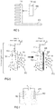
- the general principle of an arrangement for electrophoretic deposition is schematically illustrated in Figure 7 .
- the arrangement comprises a container or vessel 410.
- a coating bath or solution is held in the container or vessel 410.
- the electrically conductive surface 140 that is to be coated as well as at least one counter-electrode 150, are immersed into the coating bath or solution within the container 410.
- the electrically conductive surface 140 and the counter-electrode 150 are each connected to terminals, namely a terminal for providing a positive potential and a terminal for providing a negative potential, respectively.
- the electrically conductive surface 140 is coupled to a terminal for a negative potential (-)
- the counter-electrode 150 is coupled to a terminal for a positive potential (+), as is illustrated in Figure 7 , or vice versa.
- a direct current is applied to the electrically conductive surface 140 and to the counter-electrode 150, and, therefore, also to the solution or colloidal suspension within the container 410.
- the solution or colloidal suspension may comprise ionizable groups.
- E102PD processes There are generally two different types of E102PD processes, namely anodic and cathodic.
- anodic process negatively charged material is deposited on the positively charged electrode, or anode.
- cathodic process positively charged material is deposited on the negatively charged electrode, or cathode.
- charge destruction and the resultant decrease in solubility, concentration coagulation, and salting out are generally known in the art and will not be described in further detail herein.
- the so-called dipping-method of Figure 7 is further exemplarily illustrated in Figure 8 .
- Figure 8 illustrates a semiconductor component 100 with a semiconductor package 110 that is immersed into the solution or suspension 411 in the container 410. Although the arrow in Figure 8 indicates that the semiconductor component 100 is being immersed into the solution 411, a first layer 320 is illustrated on an outer surface of the semiconductor package 110. The first layer 320 may be formed on an electrically conductive surface of the semiconductor component 100 during the EPD process.
- a first layer 320 is formed on the outer surface of the semiconductor package 110 by depositing the first material 300 and, after depositing the first material 300, in a second step depositing a second material 310 on the first material 300 or on a pre-layer formed by the first material 300.
- the second material 310 may be a thermally conductive material with or without fillers.
- the second material 310 may be or may include a polymer.
- the polymer may be an epoxy or a silicon based polymer.
- the polymeric material maybe a soft polymeric material (flexible type polymer) or the polymeric material may be hardened.
- the second material 310 may be provided in the form of droplets or platelets, for example.
- the second step may comprise an electrophoretic deposition process, as has been described above with respect to the first step, or a dispensing method, for example.
- an electrostatic spraying method may be used, for example.
- a liquid flow emerging from a tip or thin tube 400 under the influence of a strong electric field breaks up into small droplets due to a charging of the dielectric liquid.
- this technique may be utilized to produce a polymer layer on an electrode.
- the electrode is formed by the electrically conductive surface 140 with the first pre-layer 320 (formed in step 1) deposited thereon.
- the at least one pin or lead 113 of the semiconductor component 100 may be coupled to a power supply.
- a dry powder including the second material 310, for example a polymer may be applied to the first material 300 or the first pre-layer.
- the particles in the dry powder may be electrically charged and may be attracted by the electrically conductive surface 140 when coupled to a power supply.
- the charged particles in the liquid or the powder are initially projected towards the electrically conductive surface 140 and may be accelerated towards the electrically conductive surface 140 by an electrostatic charge provided by the power supply.
- the electrically conductive surface 140 may be coupled to the positive (negatively charged particles) or the negative terminal (positively charged particles) of the power supply.
- a polymer may alternatively be deposited on the electrically conductive surface 140 using a polymer coating process or so-called e-coating method.
- Polymer coating processes generally include extrusion/dispersion coating or solution application techniques, for example.
- E-coating methods include immersing the electrically conductive surface in a bath that consists of a water-based solution, for example. An electric current is then used to attract the particles that are suspended in the liquid solution and deposit them onto the surface of the substrate. The e-coating, therefore, is very similar to the electrophoretic deposition.
- the first layer 320 includes both the first material 300 and the second material 310.
- the first step is followed by a sintering process before performing the second step.
- a sintering process is optional.
- Sintering generally is the process of compacting and forming a solid mass of material by applying heat or pressure, without melting the material to the point of liquefaction. The sintering may enhance properties such as strength and thermal conductivity, for example. If the first material includes ceramic, the sintering process at a high temperature may fuse the ceramic particles together.
- a first material 300 is deposited on an electrically conductive surface 140.
- the first step may comprise an electrophoretic deposition process, as has been described with respect to Figure 6 .
- An optional sintering step may follow (not illustrated in Figure 10 ).
- a second step illustrated in Figure 10B , a second material 310 is deposited on the first material 300 already arranged on the electrically conductive surface 140.
- the second step may comprise an electrophoretic deposition process or a dispensing method, as has been described with respect to Figure 6 above.
- the second material 310 may be deposited on the surface of a pre-layer that is formed by the first material 300.
- the pre-layer may be porous with empty spaces or cavities between the separate droplets or platelets (as illustrated in Figure 10A ), the second material 310 may at least partially fill the empty spaces or cavities of the porous pre-layer between the droplets or platelets of the first material 300, as is schematically illustrated in Figure 10B .
- the first material 300 may be or may include hexagonal boron nitride.
- the deposited first material 300 may form a hexagonal boron nitride pre-layer on the electrically conductive surface 140.
- the second material 310 may be or may include a polymer and may form a polymer coating on the first material 300.
- the resulting first layer 320 comprises the first material 300 as well as the second material 310.
- the second step may optionally be followed by a third step during which the first layer 320 comprising the first material 300 and the second material 310 is exposed to a vacuum and/or high temperatures.
- the temperatures may be room temperature (typically between 20°C and 25°C), up to 100°C, up to 150°C, up to 200°C or up to 500°C, for example.
- the third step is exemplarily illustrated in Figure 10C .
- the first layer 320 may be polymerized. Generally, during polymerization monomer molecules are reacted together in a chemical reaction to form polymer chains or three-dimensional networks. There are generally many forms of polymerization.
- the first material 300 e.g., hexagonal boron nitride
- the second material 310 e.g., polymer
- the first material 300 may be, so to speak, held in place by the second material 310.
- the structure of the first material 300 and/or the second material 310 maybe altered during the third step, as is schematically illustrated in Figure 10C . In particular, the connections between the first material 300 and the second material 310 may be altered. This may provide very good mechanical properties to the first layer 320.
- the first layer 320 may have a mass fraction of >90 wt% and provide a dense layer 320 of boron nitride and polymer on the electrically conductive surface 140. When high temperatures are used, a sintered boron nitride layer may be formed on the electrically conductive surface 140.
- the suspension that is used during the first electrophoretic deposition process may be water based, and may include a binder (e.g., cationic binder, anionic binder or uncharged binder) on a 0.1 - 60 wt% BN weight basis, for example.
- the electropohoretic deposition process using an aqueous based solution for depositing a hexagonal boron nitride filler on the electrically conductive surface 140 may be followed by a polymer coating step.
- a method may comprise an EPD (electropohoretic deposition process) boron nitride deposition followed by (i) conformal coating (dispensing or dipping), (ii) e-coating, or (iii) sintering. If options (i) or (ii) are used, an electrically isolating but thermally conductive (ceramic) layer may be formed on the electrically conductive surface 140. If option (iii) is used, a sensor coating, corrosion protection and/or mould realizing coating may be formed on the thermally conductive surface 140.
- the thickness of an electrically non-conducting thin ceramic layer of hexagonal boron nitride maybe in the range of about 1 - 20 ⁇ m, 20 - 40 ⁇ m, 40 - 100 ⁇ m or 100 - 300 ⁇ m, for example.
- a ceramic layer of hexagonal boron nitride of such a thickness may provide electrical isolation for voltages from about 0.1 - 10 kV/s.
- the electrical isolation depends on the thickness of the first material 300 (e.g., ceramic) deposited on the outer surface of the semiconductor, the first material 300 being coated by the second material 310 (e.g., polymer).
- a thermal conductivity of about 2W/mK, 10W/mK or 20W/mK may be achieved with the proposed solution, for example.
- Figure 12 shows a method for forming a matrix composite layer on a heat sink. This method is described for illustrative purposes and does not fall under the claimed invention.
- a heat sink 111 is provided.
- the heat sink 111 may be embedded in an encapsulation material of a package 210.
- the heatsink 111 may comprise a heat sink metal such as copper, nickel, tin, gold etc.
- the encapsulation material of the package 210 may include plastic, glass or ceramic, etc.
- a top surface 181 of the heat sink 111 is roughened so that the previously smooth surface of the heat sink 111 is now rough. Rough means that the surface of the heat sink includes small irregular notches, recesses or indents 182.
- the top surface 181 may have a roughness of less than 1 ⁇ m (R a ⁇ 1 (or alternatively R a ⁇ 1.5, ⁇ 2, ⁇ 3 or ⁇ 5), i.e., the arithmetical mean height is less than 1 ⁇ m.
- the surface roughness may be, however, larger than 0.025 (R a > 0.03, > 0.05 or > 0.1).
- a dam or wall 220 is formed or attached around the heat sink surface or a package 210 (embedding the heat sink) 181.
- the dam 220 may be placed around the perimeter and/or circumference of the heat sink 111.
- the dam 220 may be placed on the package 210 as shown in Figure 12C making the entire top surface 181 of the heatsink 111 (and maybe portions of the top surface of the package 210) available for deposition or dispense of the filler and plastic materials.
- the dam 220 is used for containing the later deposited or dispensed materials.
- the dam 220 may be placed only on (portions) of the top surface 211 of the package 210 material or on the (portion) of the top surface 211 of the package 210 and a portion of the top surface 181 of the heat sink 111.
- the dam 220 may be placed directly next to the perimeter of the heat sink 111 or may be laterally spaced apart from the perimeter of the heat sink 111 on the top surface 211 of the package 210 (as shown in, e.g., Figure 15A ).
- the dam 220 may comprise a crosslinking material such as an epoxy material or a polymer material.
- the dam may include silicon, acrylic, etc.
- the crosslinking material of the dam and the plastic material 350 may be the same material or a different material.
- the dam 220 may be pre-formed and adhered to the heat sink 111/package 210. Alternatively, the epoxy or polymer material is dispensed and then crosslinked by ambient temperature, heat or ultraviolet light (UV) light.
- the dam 220 may be about 220 11m high. Alternatively, the dam may have a high of 200 ⁇ m to 250 ⁇ m, 10 ⁇ m to 300 ⁇ m or 100 ⁇ m to 500 ⁇ m.
- the height of the dam 220 may depend on the height of the matrix composite layer to be deposited or dispensed.
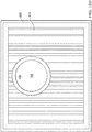
- Figure 12D shows a top view of the heat sink 111 with the dam 220.
- the dam 220 is placed around the perimeter of the heatsink 111 and around the circumference of the inner hole 183.
- the dam 220 around the perimeter and the circumference of the inner hole 183 may include the same thickness and the same height.
- the dam 220 may comprise different thicknesses and/or heights.
- a first material 340 such as a filler material is formed on the roughened surface 181 of the heat sink 111 within the and bordered by the dam 220.
- the filler material 340 may be a ceramic material.
- the ceramic material may include nitride, oxide and a carbide base material.
- the ceramic material may include (hexagonal) boron nitride, alumina oxide or alumina nitride, boron carbide.
- the filler material may be the same as previously disclosed.
- the deposition method may a dispensing method wherein the filler material 340 is dispensed by a dispenser. Alternatively, the same or similar deposition methods as previously disclosed can be used.
- the filler material 340 may be ceramic filler with or without surface coating.
- the filler material 340 (e.g., ceramic filler material) may be pretreated so that it can crosslink with a polymer.
- the filler material 340 is filled up to the height of the dam 220 or to a height lower than that of the dam 220.
- a second material 350 such as a plastic material is deposited or formed on the filler material 340.
- the plastic material 350 may a crosslinking material such an epoxy material or a polymer material.
- the plastic material 350 may be the same as previously disclosed.
- the crosslinking material 350 may be a silicone or an acrylic.
- the deposition method may a dispensing method wherein the plastic material 350 is dispensed by a dispenser. Alternatively, the same or similar deposition methods as previously disclosed can be used.
- the plastic material 350 may be the same or may be different to the material used for the dam 220.
- a matrix composite layer 360 is formed by exposing the filler material 340 and the plastic material 350 to vacuum/and or temperature so that the matrix composite layer 360 is formed on the roughened heat sink surface 181.
- the material depositions 340/350 may be cured at room temperature or at a higher temperature.
- a high or higher temperature can be a temperature in the temperature ranges of 80 °C to 120 °C, 100 °C to 150 °C or 120 °C to 200 °C.
- the material depositions 340/350 may be exposed to vacuum. Typical vacuum level ranges are provided in the following table:
- the matrix composite layer 360 disposed on the heat sink 111 is shown in Figure 12G .
- the dam 220 may remain on the heat sink 111.
- the exposure to vacuum may not be performed as a separate additional step after depositing the filler and plastic materials 340, 350 ( Figures 12E and 12F ) but rather while the filler material and the epoxy material are deposited.
- the temperature may be applied during these steps (together with the exposure to vacuum) or separately afterwards.
- the exposure to vacuum may remove air bubbles and/or other chemical additives. It is advantageous to form the matrix composite layer 360 on a roughened heat sink surface because it adheres and connects better to the heat sink 111.
- Figure 13 shows a method for forming a matrix composite layer on a heat sink. This method is described for illustrative purposes and does not fall under the claimed invention.
- Figure 13 The method of Figure 13 is the same as the one in Figure 12 with the exception of an additional step inserted between method steps Figures 12C / 13C and 12E / 13E . Accordingly, Figures 13A-13C show roughening the heat sink surface 181 and building a dam 220 around the perimeter and/or the circumference of the heat sink 111/package 210.
- a third material 370 such as a (plastic) crosslinking material, e.g., an epoxy material or a polymer material (crosslinking polymer material) is deposited or dispensed within the perimeter/circumference of or inside the dam 220.
- the third material 370 is dispensed in order to cover the rough surface 181 of the heat sink 111. This is shown in Figure 13D . This is advantageous because it provides a (air) bubble free rough top surface 181 and provides good adhesion for the matrix composite layer 360.
- the crosslinking material 370 may also be a silicone or an acrylic.
- the deposition method may be a dispensing method wherein the third material 370 is dispensed by a dispenser. Alternatively, the same or similar deposition methods as previously disclosed can be used.
- the third material 370 may be dispensed up to a height 1 ⁇ m to 10 ⁇ m or, alternatively, 0.5 ⁇ to 5 ⁇ m.
- the filler material 340 and the plastic material 350 are deposited (e.g., dispensed) and the matrix composite layer 380 is formed similar to the method disclosed in Figures 12E-12G .
- the deposition (e.g., dispense) of the filler and plastic materials 340, 350 can be performed under vacuum conditions or the deposited layer can be exposed to a vacuum and/or temperature after they are deposited.
- the third material 370, the plastic material 350 and the crosslinking material of the dam 220 may comprise the same materials or different materials.
- Figure 14 shows a method for forming a matrix composite layer on a heat sink. This method is described for illustrative purposes and does not fall under the claimed invention.
- a roughened heat sink 111 is provided.
- the heat sink 111 may be embedded in an encapsulation material of the package 210.
- the heatsink 111 may comprise a heat sink metal such as copper, nickel, tin, gold, etc.
- the encapsulation material of the package 210 may include plastic, glass or ceramic, etc.
- the heat sink 111 may be roughened according to a procedure discussed in Figure 12B .
- a clamper 390 such as a side wall clamper grabs or grasps the heatsink 111 or clamps to the package 210 surrounding the heat sink 111.
- the clamper 390 may grab, grasp or clamp to the heat sink 111 at a sidewall of the heat sink 111 or at the sidewall of the package 210.
- the clamper 390 maybe a jig clamper (prefix jig from side or top package to create required shape). Other clampers 390 may be used.
- the clamper 390 may grab or grasps the heat sink/package 111/210 in an angle between equal or more than 3° degree and equal or less than 10°.
- the clamper 390 may grab or grasps the heat sink/package 111/210 in an angle between equal or more than 5° degree and equal or less than 15°. Clamping the heat sink/package 111/210 with an angle is advantageous because the clamper 390 can be easier released compared to a clamper having not such an angle.
- the clamper 390 may clamp to the outer sidewall and the inner hole 183 of the heat sink/package 111/210 at the same time so that so that walls are formed similar to that of the dam 210.
- the clamper 390 is used for containing the later deposited or dispensed materials.
- the filler material 340 and the plastic material 350 deposited (e.g., dispensed) and the matrix composite layer 360/380 is formed similar to the method disclosed in Figures 12E-12G .
- the deposition (e.g., dispensing) of the filler and plastic materials 340/350 can be performed under vacuum conditions or the deposited (e.g., dispensed) layers can be exposed to vacuum and/or temperature after they are deposited.
- an epoxy material 370 can be deposited similar to that shown in Figure 13D .
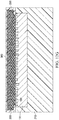
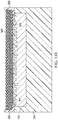
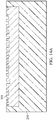
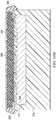
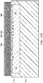
- Figures 15A-15D show different types of filler materials in the matrix composite layer disposed on the heat sink.
- Figures 15A and 15B illustrate matrix composite layers 385/386 disposed on the heat sink 111, wherein the filler materials 355/356 comprise individual spherical filler particles or individual platelet filler particles (e.g., ceramic particles).
- the filler particles may be circular or oval, ball shaped or ellipsoid.
- the filer particles maybe a polygon platelet or a three dimensional polygon.
- the filler particles 355 may comprise substantially the same size as shown in Figure 15A or different sizes as shown in Figure 15B .
- the particles may be aligned in specific direction, or randomly or irregularly distributed (no main direction).
- Figure 15A shows oval or ellipsoid particles 355 having the substantially the same size aligned with their main direction parallel to the top surface 181 of the heat sink 111.
- Figure 15B shows ball shaped/circular and ellipsoid/oval particles 356 of different sizes randomly distributed with no particular preferred alignment.
- Figure 15C illustrates a matrix composite layer 387 having a filler material 357 of agglomerated spherical/platelet filler particles (e.g., ceramic particles).
- the agglomerated particles 357 may be disposed such that their main direction is aligned and that they are aligned sphere or round shape to the top surface 181 of the heat sink 111. Again, the agglomerated particles 357 themselves may comprise substantially the same size or different size. Similarly, the particles in the agglomerated particles 357 may comprise substantially the same size or different sizes.
- Figure 15D illustrates a matrix composite layer 388 having agglomerated spherical/platelet filler particles 357 (e.g., ceramic particles) and individual filler particles 355/356. Any combination of these different particles is possible.
- aligned individual filler particles can be combined with aligned agglomerated filler particles (e.g., aligned orthogonal to each other), aligned agglomerated filler particles can be combined randomly distributed individual filler particles (having, e.g., the same or different sizes), etc.
- the agglomerated filler particles 357 may be disposed on certain regions 391 on the surface 181 of the heat sink 111 and the individual filler particles 355/356 may be disposed on other regions 392 of the surface 181 of the heat sink 111.
- the thermal conductivity and/or the electrical insolation of the matrix composite layer 388 can be configured.
- the thermal conductivity and/or electrical isolation of the matrix composite layer 388 in the regions 392 where the individual filler particles 355/356 are disposed may be higher than the thermal conductivity of the matrix composite layer 388 in regions 391 where the agglomerated particles 357 are located (or vice versa).
- the thermal conductivity and/or electrical isolation of the matrix composite layer 388 in the regions 392 where the filler particles are aligned 355 may be higher than the thermal conductivity and/or electrical isolation of the matrix composite layer 388 in regions 392 where the filler particles 355 are not aligned (or vice versa).
- the matrix composite layer 388 can be configures or arranged such that the regions where a package 110 is attached to the heat sink 111 has a high thermal conductivity and a high electrical isolation while areas where no package is attached to the heat sink 111 has a high thermal conductivity and an electrically conductive, for example.
- the embodiment methods for forming a matrix composite layer on a heat sink 111 can also be performed to form a matrix composite layer on the heat sink 140 of the package 110.
- the matrix composite layer is a layer with a high filler content.
- the filler content may be equal or more than 30 wt%, equal or more than 80 wt%, equal or more than 90 wt%, or equal or more than 95 wt%.
- the electrical isolation of the matrix composite layer depends on the thickness of the layer, i.e., the thicker the layer the better the electrical isolation.
- a thermally conductive layer is formed on an outer surface of a semiconductor package, by depositing a first material on the outer surface of the semiconductor package, and depositing a second material on the first material after depositing the first material.
- the first thermally conductive layer may be formed by an electrophoretic deposition process.
- Depositing the first material may form a porous pre-layer on the outer surface of the semiconductor package.
- the porous pre-layer may comprise cavities and depositing the second material on the first material may at least partially fill the cavities of the pre-layer.
- the first material may be deposited by an electrophoretic deposition process.
- the first material may comprise at least one of boron nitride, aluminium oxide, silicon carbide, silicon dioxide, or a ceramic material including an oxide or nitride combination.
- the second material may be deposited on the first material by at least one of an electrophoretic deposition process, an e-coating process, a dispensing method, an electrostatic spraying method or a dipping method.
- the second material may be a thermally conductive material with or without fillers or a polymer.
- the first material may be sintered after being deposited. After depositing the second material, the first and the second material may be heated and/or exposed to a vacuum.
- the thermal conductivity of the first thermally conductive layer may be dependent on the first thickness of the first material.
- the outer surface of the semiconductor package may be electrically conductive, and may take the form of a heat sink or a die pad of the semiconductor package.
- the first thermally conductive layer may be formed by applying a direct current to the electrically conductive surface, and may be configured to be mounted to an external heat sink.
- the first thermally conductive layer may include a first material comprising a porous pre-layer disposed on the outer surface of the semiconductor package and a second material disposed over the first material.
- the porous pre-layer may comprises cavities and the second material may at least partially fill the cavities of the porous pre-layer.
- the first material may include at least one of boron nitride, aluminium oxide, silicon carbide, silicon dioxide, or a ceramic material including an oxide or a nitride combination.
- the second material may be a polymer, or a thermally conductive material with or without fillers.
- the outer surface of the package may include an electrically conductive surface, which may take the form of a heat sink or a die pad of the semiconductor component.
- the semiconductor component may be configured to be mounted to an external heat sink such that the first thermally conductive layer faces the external heat sink.
Landscapes
- Chemical & Material Sciences (AREA)
- Engineering & Computer Science (AREA)
- Composite Materials (AREA)
- Mechanical Engineering (AREA)
- Cooling Or The Like Of Semiconductors Or Solid State Devices (AREA)
- Materials Engineering (AREA)
- Laminated Bodies (AREA)
- Chemically Coating (AREA)
Claims (9)
- Verfahren, welches umfasst:
Bilden einer ersten thermisch leitenden Schicht (320) auf einer Außenoberfläche (140) eines Halbleitergehäuses (110), wobei das Bilden der ersten thermisch leitenden Schicht (320) umfasst:Aufbringen eines ersten Materials (300) auf die Außenoberfläche (140) des Halbleitergehäuses (110); undAufbringen eines zweiten Materials (310) auf das erste Material (300) nach dem Aufbringen des ersten Materials (300),wobei das erste Material (300) mindestens eines der folgenden umfasst:Bornitrid,Aluminiumoxid,Siliziumkarbid,Siliziumdioxid, oderein keramisches Material, welches eine Oxid- oder Nitridkombination enthält. - Verfahren gemäß Anspruch 1, wobei mindestens:das Bilden der ersten thermisch leitenden Schicht (320) ein elektrophoretisches Abscheidungsverfahren umfasst;das Aufbringen des ersten Materials (300) das Bilden einer porösen Vorschicht auf die Außenoberfläche (140) des Halbleitergehäuses (110) umfasst; oderdas Aufbringen des ersten Materials (300) ein elektrophoretisches Abscheidungsverfahren umfasst.
- Verfahren gemäß Anspruch 2, wobei die poröse Vorschicht Hohlräume aufweist und das Aufbringen des zweiten Materials (310) auf das erste Material (300) das mindestens teilweise Füllen der Hohlräume der Vorschicht umfasst.
- Verfahren gemäß einem der Ansprüche 1 bis 3, wobei mindestens:das Aufbringen des zweiten Materials (310) auf das erste Material (300) ein elektrophoretisches Abscheidungsverfahren umfasst;das Aufbringen des zweiten Materials (310) auf das erste Material (300) ein Elektrobeschichtungsverfahren umfasst;das Aufbringen des zweiten Materials (310) auf das erste Material (300) ein Dosierungsverfahren umfasst;das Aufbringen des zweiten Materials (310) auf das erste Material (300) ein elektrostatisches Sprühverfahren umfasst;das Aufbringen des zweiten Materials (310) auf das erste Material (300) ein Tauchverfahren umfasst; oderdas zweite Material (310) ein thermisch leitfähiges Material mit oder ohne Füllstoff oder ein Polymer umfasst.
- Verfahren gemäß einem der vorherigen Ansprüche, wobei das Verfahren weiter mindestens eines der folgenden umfasst:nach dem Aufbringen des ersten Materials (300), Sintern des ersten Materials (300);nach dem Aufbringen des zweiten Materials (300), Erhitzen des ersten und des zweiten Materials (300, 310); odernach dem Aufbringen des zweiten Materials (300), Aussetzen des ersten und des zweiten Materials (300, 310) einem Vakuum.
- Verfahren gemäß einem der vorherigen Ansprüche, wobei das erste Material (300), welches auf die Außenoberfläche (140) des Halbleitergehäuses (110) aufgebracht wird, eine erste Schichtdicke aufweist, und wobei die thermische Leitfähigkeit der ersten thermisch leitenden Schicht (320) von der ersten Schichtdicke abhängig ist.
- Verfahren gemäß einem der vorherigen Ansprüche, wobei die Außenoberfläche (140) des Halbleitergehäuses (110) eine elektrisch leitende Oberfläche aufweist.
- Verfahren gemäß Anspruch 7, wobei mindestens:die elektrisch leitende Oberfläche ein Kühlkörper oder ein Chip-Pad des Halbleitergehäuses (110) ist; unddas Bilden der ersten thermisch leitenden Schicht (320) das Anlegen eines direkten Stroms an die elektrisch leitende Oberfläche umfasst.
- Verfahren gemäß einem der vorherigen Ansprüche, wobei die erste thermisch leitende Schicht (320), welche auf der Außenoberfläche (140) des Halbleitergehäuses (110) gebildet wird, dazu ausgebildet ist, an einem äußerem Kühlkörper (111) angeordnet zu werden.
Priority Applications (2)
| Application Number | Priority Date | Filing Date | Title |
|---|---|---|---|
| EP19207250.2A EP3627547B1 (de) | 2017-04-13 | 2018-04-12 | Verfahren zur ausbildung einer verbundschicht |
| EP19207243.7A EP3629371A3 (de) | 2017-04-13 | 2018-04-12 | Kühlkörperanordnung |
Applications Claiming Priority (2)
| Application Number | Priority Date | Filing Date | Title |
|---|---|---|---|
| US15/486,907 US10121723B1 (en) | 2017-04-13 | 2017-04-13 | Semiconductor component and method for producing a semiconductor component |
| US15/944,549 US10457001B2 (en) | 2017-04-13 | 2018-04-03 | Method for forming a matrix composite layer and workpiece with a matrix composite layer |
Related Child Applications (2)
| Application Number | Title | Priority Date | Filing Date |
|---|---|---|---|
| EP19207243.7A Division EP3629371A3 (de) | 2017-04-13 | 2018-04-12 | Kühlkörperanordnung |
| EP19207250.2A Division EP3627547B1 (de) | 2017-04-13 | 2018-04-12 | Verfahren zur ausbildung einer verbundschicht |
Publications (2)
| Publication Number | Publication Date |
|---|---|
| EP3389086A1 EP3389086A1 (de) | 2018-10-17 |
| EP3389086B1 true EP3389086B1 (de) | 2019-11-06 |
Family
ID=61972346
Family Applications (3)
| Application Number | Title | Priority Date | Filing Date |
|---|---|---|---|
| EP19207243.7A Pending EP3629371A3 (de) | 2017-04-13 | 2018-04-12 | Kühlkörperanordnung |
| EP18166919.3A Active EP3389086B1 (de) | 2017-04-13 | 2018-04-12 | Verfahren zur herstellung einer verbundschicht und werkstück mit einer verbundschicht |
| EP19207250.2A Active EP3627547B1 (de) | 2017-04-13 | 2018-04-12 | Verfahren zur ausbildung einer verbundschicht |
Family Applications Before (1)
| Application Number | Title | Priority Date | Filing Date |
|---|---|---|---|
| EP19207243.7A Pending EP3629371A3 (de) | 2017-04-13 | 2018-04-12 | Kühlkörperanordnung |
Family Applications After (1)
| Application Number | Title | Priority Date | Filing Date |
|---|---|---|---|
| EP19207250.2A Active EP3627547B1 (de) | 2017-04-13 | 2018-04-12 | Verfahren zur ausbildung einer verbundschicht |
Country Status (3)
| Country | Link |
|---|---|
| US (1) | US10457001B2 (de) |
| EP (3) | EP3629371A3 (de) |
| CN (1) | CN108735613B (de) |
Families Citing this family (5)
| Publication number | Priority date | Publication date | Assignee | Title |
|---|---|---|---|---|
| US10457001B2 (en) * | 2017-04-13 | 2019-10-29 | Infineon Technologies Ag | Method for forming a matrix composite layer and workpiece with a matrix composite layer |
| US10903184B2 (en) * | 2018-08-22 | 2021-01-26 | International Business Machines Corporation | Filler particle position and density manipulation with applications in thermal interface materials |
| TW202543812A (zh) * | 2019-10-25 | 2025-11-16 | 德商漢高股份有限及兩合公司 | 可三維圖案化之熱介面 |
| WO2021173991A1 (en) * | 2020-02-26 | 2021-09-02 | Ppg Industries Ohio, Inc. | Two-layer dielectric coating |
| CN113539995B (zh) * | 2021-07-16 | 2024-04-12 | 威星国际半导体(深圳)有限公司 | 一种高导热率碳化硅器件封装结构及方法 |
Family Cites Families (39)
| Publication number | Priority date | Publication date | Assignee | Title |
|---|---|---|---|---|
| GB644167A (en) * | 1947-08-09 | 1950-10-04 | Sprague Electric Co | Improvements in electrical conductors |
| US5561322A (en) * | 1994-11-09 | 1996-10-01 | International Business Machines Corporation | Semiconductor chip package with enhanced thermal conductivity |
| DE19529627C1 (de) * | 1995-08-11 | 1997-01-16 | Siemens Ag | Thermisch leitende, elektrisch isolierende Verbindung und Verfahren zu seiner Herstellung |
| JP3223835B2 (ja) * | 1997-03-28 | 2001-10-29 | 三菱電機株式会社 | パワー半導体装置及びその製造方法 |
| US6160042A (en) | 1997-05-01 | 2000-12-12 | Edison Polymer Innovation Corporation | Surface treated boron nitride for forming a low viscosity high thermal conductivity polymer based boron nitride composition and method |
| US5945217A (en) | 1997-10-14 | 1999-08-31 | Gore Enterprise Holdings, Inc. | Thermally conductive polytrafluoroethylene article |
| CA2614620C (en) * | 2000-05-10 | 2010-02-02 | Alberta Research Council Inc. | Production of hollow ceramic membranes by electrophoretic deposition |
| JP2002033558A (ja) * | 2000-07-18 | 2002-01-31 | Matsushita Electric Ind Co Ltd | 回路基板とその製造方法 |
| US6400014B1 (en) * | 2001-01-13 | 2002-06-04 | Siliconware Precision Industries Co., Ltd. | Semiconductor package with a heat sink |
| US6846588B2 (en) * | 2002-01-16 | 2005-01-25 | Alberta Research Council Inc. | Hollow inorganic membranes produced by metal or composite electrodeposition |
| US6946190B2 (en) * | 2002-02-06 | 2005-09-20 | Parker-Hannifin Corporation | Thermal management materials |
| US7927424B2 (en) * | 2002-04-22 | 2011-04-19 | Stmicroelectronics, Inc. | Padded clamp ring with edge exclusion for deposition of thick AlCu/AlSiCu/Cu metal alloy layers |
| KR100902766B1 (ko) * | 2002-09-27 | 2009-06-15 | 페어차일드코리아반도체 주식회사 | 절연성 세라믹 히트 싱크를 갖는 디스크리트 패키지 |
| US7013965B2 (en) | 2003-04-29 | 2006-03-21 | General Electric Company | Organic matrices containing nanomaterials to enhance bulk thermal conductivity |
| US7494635B2 (en) | 2003-08-21 | 2009-02-24 | Saint-Gobain Ceramics & Plastics, Inc. | Boron nitride agglomerated powder |
| US7550097B2 (en) | 2003-09-03 | 2009-06-23 | Momentive Performance Materials, Inc. | Thermal conductive material utilizing electrically conductive nanoparticles |
| US20050127134A1 (en) * | 2003-09-15 | 2005-06-16 | Guo-Quan Lu | Nano-metal composite made by deposition from colloidal suspensions |
| CN101595557A (zh) * | 2006-08-11 | 2009-12-02 | 威世通用半导体公司 | 半导体器件及用于制造具有改善的散热能力的半导体器件的方法 |
| US7629676B2 (en) * | 2006-09-07 | 2009-12-08 | Infineon Technologies Ag | Semiconductor component having a semiconductor die and a leadframe |
| US20090236757A1 (en) * | 2008-03-24 | 2009-09-24 | Infineon Technologies Ag | Semiconductor device and method for manufacturing |
| CN201349384Y (zh) * | 2008-12-24 | 2009-11-18 | 彭泰企业有限公司 | 高导散热铝覆金属底材结构 |
| DE102009014794B3 (de) * | 2009-03-28 | 2010-11-11 | Danfoss Silicon Power Gmbh | Verfahren zum Herstellen eines für Hochvoltanwendungen geeigneten festen Leistungsmoduls und damit hergestelltes Leistungsmodul |
| CN101916731B (zh) * | 2010-07-12 | 2012-07-04 | 深圳大学 | 一种陶瓷绝缘膜导热基板及其制作方法 |
| US8569109B2 (en) * | 2011-06-30 | 2013-10-29 | Infineon Technologies Ag | Method for attaching a metal surface to a carrier, a method for attaching a chip to a chip carrier, a chip-packaging module and a packaging module |
| US8587945B1 (en) | 2012-07-27 | 2013-11-19 | Outlast Technologies Llc | Systems structures and materials for electronic device cooling |
| KR102005234B1 (ko) * | 2012-09-25 | 2019-07-30 | 삼성전자주식회사 | 가이드 벽을 갖는 반도체 패키지 |
| US9303327B2 (en) * | 2013-01-10 | 2016-04-05 | Infineon Technologies Ag | Electric component with an electrophoretically deposited film |
| US9316382B2 (en) | 2013-01-31 | 2016-04-19 | Cree, Inc. | Connector devices, systems, and related methods for connecting light emitting diode (LED) modules |
| US8907472B2 (en) * | 2013-02-07 | 2014-12-09 | Taiwan Semiconductor Manufacturing Company, Ltd. | 3DIC package comprising perforated foil sheet |
| CN105026312B (zh) | 2013-03-07 | 2018-03-20 | 电化株式会社 | 氮化硼粉末及含有该氮化硼粉末的树脂组合物 |
| KR101625264B1 (ko) | 2013-05-30 | 2016-05-27 | 제일모직주식회사 | 방열 접착 필름, 이를 포함하는 반도체 장치 및 상기 장치의 제조 방법 |
| US9420731B2 (en) * | 2013-09-18 | 2016-08-16 | Infineon Technologies Austria Ag | Electronic power device and method of fabricating an electronic power device |
| US9576930B2 (en) * | 2013-11-08 | 2017-02-21 | Taiwan Semiconductor Manufacturing Co., Ltd. | Thermally conductive structure for heat dissipation in semiconductor packages |
| JP6345265B2 (ja) * | 2014-10-29 | 2018-06-20 | 日立オートモティブシステムズ株式会社 | 電子機器及び電子機器の製造方法 |
| US11060805B2 (en) | 2014-12-12 | 2021-07-13 | Teledyne Scientific & Imaging, Llc | Thermal interface material system |
| DE102015108700B4 (de) * | 2015-06-02 | 2025-01-09 | Infineon Technologies Austria Ag | Halbleiter-Leistungs-Package und Verfahren zu ihrer Herstellung |
| DE102015118245B4 (de) | 2015-10-26 | 2024-10-10 | Infineon Technologies Austria Ag | Elektronische Komponente mit einem thermischen Schnittstellenmaterial, Herstellungsverfahren für eine elektronische Komponente, Wärmeabfuhrkörper mit einem thermischen Schnittstellenmaterial und thermisches Schnittstellenmaterial |
| TWI584428B (zh) * | 2016-06-08 | 2017-05-21 | 力成科技股份有限公司 | 降低封裝翹曲之散熱型半導體封裝構造 |
| US10457001B2 (en) * | 2017-04-13 | 2019-10-29 | Infineon Technologies Ag | Method for forming a matrix composite layer and workpiece with a matrix composite layer |
-
2018
- 2018-04-03 US US15/944,549 patent/US10457001B2/en active Active
- 2018-04-12 EP EP19207243.7A patent/EP3629371A3/de active Pending
- 2018-04-12 EP EP18166919.3A patent/EP3389086B1/de active Active
- 2018-04-12 EP EP19207250.2A patent/EP3627547B1/de active Active
- 2018-04-13 CN CN201810330464.7A patent/CN108735613B/zh active Active
Non-Patent Citations (1)
| Title |
|---|
| None * |
Also Published As
| Publication number | Publication date |
|---|---|
| EP3627547B1 (de) | 2025-08-06 |
| US20180297301A1 (en) | 2018-10-18 |
| CN108735613B (zh) | 2024-07-12 |
| EP3627547A2 (de) | 2020-03-25 |
| EP3389086A1 (de) | 2018-10-17 |
| CN108735613A (zh) | 2018-11-02 |
| EP3629371A3 (de) | 2020-07-29 |
| US10457001B2 (en) | 2019-10-29 |
| EP3629371A2 (de) | 2020-04-01 |
| EP3627547A3 (de) | 2020-11-04 |
Similar Documents
| Publication | Publication Date | Title |
|---|---|---|
| EP3627547B1 (de) | Verfahren zur ausbildung einer verbundschicht | |
| US5367196A (en) | Molded plastic semiconductor package including an aluminum alloy heat spreader | |
| US20210020541A1 (en) | Thermal interface material having defined thermal, mechanical and electric properties | |
| US5608267A (en) | Molded plastic semiconductor package including heat spreader | |
| CN100343987C (zh) | 具有金属板和半导体芯片的半导体器件 | |
| CN1996585B (zh) | 具有嵌入到塑料壳体中的半导体结构组件的半导体构件 | |
| US9076780B2 (en) | Power module and lead frame for power module | |
| US8017446B2 (en) | Method for manufacturing a rigid power module suited for high-voltage applications | |
| JP5640281B2 (ja) | パッケージ基板及びその製造方法 | |
| JPH05501638A (ja) | 金属製ピン格子列パッケージ | |
| CN102656945B (zh) | 具有电连接元件的板 | |
| CN103943575A (zh) | 用于在暴露的导电表面上电泳沉积(epd)薄膜的方法及其电子部件 | |
| CN103517542A (zh) | 电路板、具有该电路板的电子模块、照明装置和制造该电路板的方法 | |
| CN111403348B (zh) | 一种含微通道的陶瓷基板及其制备方法 | |
| CN108807301A (zh) | 使用烧结附着的封装微电子组件安装 | |
| KR20180014081A (ko) | 개방-세공 콘택 피스의 갈바닉 연결에 의하여 컴포넌트를 전기적으로 콘택팅하기 위한 방법, 및 대응하는 컴포넌트 모듈 | |
| KR102829764B1 (ko) | 고열 플럭스 다부품 조립체의 열 관리 | |
| CN102683546B (zh) | 半导体封装结构与其制造方法 | |
| US10121723B1 (en) | Semiconductor component and method for producing a semiconductor component | |
| JP6021745B2 (ja) | 冷却部材および半導体装置 | |
| JP2006518553A (ja) | 熱相互接続システムの生成方法およびその使用法 | |
| CN114121392A (zh) | 热敏电阻元件及其制造方法 | |
| CN102084481B (zh) | 用于高温应用的平面电功率电子模块以及相应的制造方法 | |
| JP2017001310A (ja) | 熱伝導性に優れた陽極酸化皮膜及びそれを含む積層構造体 | |
| EP4614551A1 (de) | Substrat und verfahren zur herstellung eines substrats |
Legal Events
| Date | Code | Title | Description |
|---|---|---|---|
| PUAI | Public reference made under article 153(3) epc to a published international application that has entered the european phase |
Free format text: ORIGINAL CODE: 0009012 |
|
| STAA | Information on the status of an ep patent application or granted ep patent |
Free format text: STATUS: THE APPLICATION HAS BEEN PUBLISHED |
|
| AK | Designated contracting states |
Kind code of ref document: A1 Designated state(s): AL AT BE BG CH CY CZ DE DK EE ES FI FR GB GR HR HU IE IS IT LI LT LU LV MC MK MT NL NO PL PT RO RS SE SI SK SM TR |
|
| AX | Request for extension of the european patent |
Extension state: BA ME |
|
| STAA | Information on the status of an ep patent application or granted ep patent |
Free format text: STATUS: REQUEST FOR EXAMINATION WAS MADE |
|
| 17P | Request for examination filed |
Effective date: 20190416 |
|
| RBV | Designated contracting states (corrected) |
Designated state(s): AL AT BE BG CH CY CZ DE DK EE ES FI FR GB GR HR HU IE IS IT LI LT LU LV MC MK MT NL NO PL PT RO RS SE SI SK SM TR |
|
| GRAP | Despatch of communication of intention to grant a patent |
Free format text: ORIGINAL CODE: EPIDOSNIGR1 |
|
| STAA | Information on the status of an ep patent application or granted ep patent |
Free format text: STATUS: GRANT OF PATENT IS INTENDED |
|
| INTG | Intention to grant announced |
Effective date: 20190531 |
|
| GRAS | Grant fee paid |
Free format text: ORIGINAL CODE: EPIDOSNIGR3 |
|
| GRAA | (expected) grant |
Free format text: ORIGINAL CODE: 0009210 |
|
| STAA | Information on the status of an ep patent application or granted ep patent |
Free format text: STATUS: THE PATENT HAS BEEN GRANTED |
|
| AK | Designated contracting states |
Kind code of ref document: B1 Designated state(s): AL AT BE BG CH CY CZ DE DK EE ES FI FR GB GR HR HU IE IS IT LI LT LU LV MC MK MT NL NO PL PT RO RS SE SI SK SM TR |
|
| REG | Reference to a national code |
Ref country code: GB Ref legal event code: FG4D |
|
| REG | Reference to a national code |
Ref country code: CH Ref legal event code: EP Ref country code: AT Ref legal event code: REF Ref document number: 1199970 Country of ref document: AT Kind code of ref document: T Effective date: 20191115 |
|
| REG | Reference to a national code |
Ref country code: IE Ref legal event code: FG4D |
|
| REG | Reference to a national code |
Ref country code: DE Ref legal event code: R096 Ref document number: 602018001080 Country of ref document: DE |
|
| REG | Reference to a national code |
Ref country code: NL Ref legal event code: MP Effective date: 20191106 |
|
| REG | Reference to a national code |
Ref country code: LT Ref legal event code: MG4D |
|
| PG25 | Lapsed in a contracting state [announced via postgrant information from national office to epo] |
Ref country code: BG Free format text: LAPSE BECAUSE OF FAILURE TO SUBMIT A TRANSLATION OF THE DESCRIPTION OR TO PAY THE FEE WITHIN THE PRESCRIBED TIME-LIMIT Effective date: 20200206 Ref country code: NO Free format text: LAPSE BECAUSE OF FAILURE TO SUBMIT A TRANSLATION OF THE DESCRIPTION OR TO PAY THE FEE WITHIN THE PRESCRIBED TIME-LIMIT Effective date: 20200206 Ref country code: FI Free format text: LAPSE BECAUSE OF FAILURE TO SUBMIT A TRANSLATION OF THE DESCRIPTION OR TO PAY THE FEE WITHIN THE PRESCRIBED TIME-LIMIT Effective date: 20191106 Ref country code: PT Free format text: LAPSE BECAUSE OF FAILURE TO SUBMIT A TRANSLATION OF THE DESCRIPTION OR TO PAY THE FEE WITHIN THE PRESCRIBED TIME-LIMIT Effective date: 20200306 Ref country code: LV Free format text: LAPSE BECAUSE OF FAILURE TO SUBMIT A TRANSLATION OF THE DESCRIPTION OR TO PAY THE FEE WITHIN THE PRESCRIBED TIME-LIMIT Effective date: 20191106 Ref country code: SE Free format text: LAPSE BECAUSE OF FAILURE TO SUBMIT A TRANSLATION OF THE DESCRIPTION OR TO PAY THE FEE WITHIN THE PRESCRIBED TIME-LIMIT Effective date: 20191106 Ref country code: NL Free format text: LAPSE BECAUSE OF FAILURE TO SUBMIT A TRANSLATION OF THE DESCRIPTION OR TO PAY THE FEE WITHIN THE PRESCRIBED TIME-LIMIT Effective date: 20191106 Ref country code: LT Free format text: LAPSE BECAUSE OF FAILURE TO SUBMIT A TRANSLATION OF THE DESCRIPTION OR TO PAY THE FEE WITHIN THE PRESCRIBED TIME-LIMIT Effective date: 20191106 Ref country code: GR Free format text: LAPSE BECAUSE OF FAILURE TO SUBMIT A TRANSLATION OF THE DESCRIPTION OR TO PAY THE FEE WITHIN THE PRESCRIBED TIME-LIMIT Effective date: 20200207 Ref country code: PL Free format text: LAPSE BECAUSE OF FAILURE TO SUBMIT A TRANSLATION OF THE DESCRIPTION OR TO PAY THE FEE WITHIN THE PRESCRIBED TIME-LIMIT Effective date: 20191106 |
|
| PG25 | Lapsed in a contracting state [announced via postgrant information from national office to epo] |
Ref country code: RS Free format text: LAPSE BECAUSE OF FAILURE TO SUBMIT A TRANSLATION OF THE DESCRIPTION OR TO PAY THE FEE WITHIN THE PRESCRIBED TIME-LIMIT Effective date: 20191106 Ref country code: HR Free format text: LAPSE BECAUSE OF FAILURE TO SUBMIT A TRANSLATION OF THE DESCRIPTION OR TO PAY THE FEE WITHIN THE PRESCRIBED TIME-LIMIT Effective date: 20191106 Ref country code: IS Free format text: LAPSE BECAUSE OF FAILURE TO SUBMIT A TRANSLATION OF THE DESCRIPTION OR TO PAY THE FEE WITHIN THE PRESCRIBED TIME-LIMIT Effective date: 20200306 |
|
| PG25 | Lapsed in a contracting state [announced via postgrant information from national office to epo] |
Ref country code: AL Free format text: LAPSE BECAUSE OF FAILURE TO SUBMIT A TRANSLATION OF THE DESCRIPTION OR TO PAY THE FEE WITHIN THE PRESCRIBED TIME-LIMIT Effective date: 20191106 |
|
| PG25 | Lapsed in a contracting state [announced via postgrant information from national office to epo] |
Ref country code: CZ Free format text: LAPSE BECAUSE OF FAILURE TO SUBMIT A TRANSLATION OF THE DESCRIPTION OR TO PAY THE FEE WITHIN THE PRESCRIBED TIME-LIMIT Effective date: 20191106 Ref country code: ES Free format text: LAPSE BECAUSE OF FAILURE TO SUBMIT A TRANSLATION OF THE DESCRIPTION OR TO PAY THE FEE WITHIN THE PRESCRIBED TIME-LIMIT Effective date: 20191106 Ref country code: RO Free format text: LAPSE BECAUSE OF FAILURE TO SUBMIT A TRANSLATION OF THE DESCRIPTION OR TO PAY THE FEE WITHIN THE PRESCRIBED TIME-LIMIT Effective date: 20191106 Ref country code: EE Free format text: LAPSE BECAUSE OF FAILURE TO SUBMIT A TRANSLATION OF THE DESCRIPTION OR TO PAY THE FEE WITHIN THE PRESCRIBED TIME-LIMIT Effective date: 20191106 Ref country code: DK Free format text: LAPSE BECAUSE OF FAILURE TO SUBMIT A TRANSLATION OF THE DESCRIPTION OR TO PAY THE FEE WITHIN THE PRESCRIBED TIME-LIMIT Effective date: 20191106 |
|
| REG | Reference to a national code |
Ref country code: DE Ref legal event code: R097 Ref document number: 602018001080 Country of ref document: DE |
|
| REG | Reference to a national code |
Ref country code: AT Ref legal event code: MK05 Ref document number: 1199970 Country of ref document: AT Kind code of ref document: T Effective date: 20191106 |
|
| PG25 | Lapsed in a contracting state [announced via postgrant information from national office to epo] |
Ref country code: SM Free format text: LAPSE BECAUSE OF FAILURE TO SUBMIT A TRANSLATION OF THE DESCRIPTION OR TO PAY THE FEE WITHIN THE PRESCRIBED TIME-LIMIT Effective date: 20191106 Ref country code: SK Free format text: LAPSE BECAUSE OF FAILURE TO SUBMIT A TRANSLATION OF THE DESCRIPTION OR TO PAY THE FEE WITHIN THE PRESCRIBED TIME-LIMIT Effective date: 20191106 |
|
| PLBE | No opposition filed within time limit |
Free format text: ORIGINAL CODE: 0009261 |
|
| STAA | Information on the status of an ep patent application or granted ep patent |
Free format text: STATUS: NO OPPOSITION FILED WITHIN TIME LIMIT |
|
| 26N | No opposition filed |
Effective date: 20200807 |
|
| PG25 | Lapsed in a contracting state [announced via postgrant information from national office to epo] |
Ref country code: AT Free format text: LAPSE BECAUSE OF FAILURE TO SUBMIT A TRANSLATION OF THE DESCRIPTION OR TO PAY THE FEE WITHIN THE PRESCRIBED TIME-LIMIT Effective date: 20191106 Ref country code: SI Free format text: LAPSE BECAUSE OF FAILURE TO SUBMIT A TRANSLATION OF THE DESCRIPTION OR TO PAY THE FEE WITHIN THE PRESCRIBED TIME-LIMIT Effective date: 20191106 Ref country code: MC Free format text: LAPSE BECAUSE OF FAILURE TO SUBMIT A TRANSLATION OF THE DESCRIPTION OR TO PAY THE FEE WITHIN THE PRESCRIBED TIME-LIMIT Effective date: 20191106 |
|
| PG25 | Lapsed in a contracting state [announced via postgrant information from national office to epo] |
Ref country code: LU Free format text: LAPSE BECAUSE OF NON-PAYMENT OF DUE FEES Effective date: 20200412 Ref country code: IT Free format text: LAPSE BECAUSE OF FAILURE TO SUBMIT A TRANSLATION OF THE DESCRIPTION OR TO PAY THE FEE WITHIN THE PRESCRIBED TIME-LIMIT Effective date: 20191106 |
|
| REG | Reference to a national code |
Ref country code: BE Ref legal event code: MM Effective date: 20200430 |
|
| PG25 | Lapsed in a contracting state [announced via postgrant information from national office to epo] |
Ref country code: BE Free format text: LAPSE BECAUSE OF NON-PAYMENT OF DUE FEES Effective date: 20200430 |
|
| PG25 | Lapsed in a contracting state [announced via postgrant information from national office to epo] |
Ref country code: IE Free format text: LAPSE BECAUSE OF NON-PAYMENT OF DUE FEES Effective date: 20200412 |
|
| PG25 | Lapsed in a contracting state [announced via postgrant information from national office to epo] |
Ref country code: CH Free format text: LAPSE BECAUSE OF NON-PAYMENT OF DUE FEES Effective date: 20210430 Ref country code: LI Free format text: LAPSE BECAUSE OF NON-PAYMENT OF DUE FEES Effective date: 20210430 |
|
| PG25 | Lapsed in a contracting state [announced via postgrant information from national office to epo] |
Ref country code: TR Free format text: LAPSE BECAUSE OF FAILURE TO SUBMIT A TRANSLATION OF THE DESCRIPTION OR TO PAY THE FEE WITHIN THE PRESCRIBED TIME-LIMIT Effective date: 20191106 Ref country code: MT Free format text: LAPSE BECAUSE OF FAILURE TO SUBMIT A TRANSLATION OF THE DESCRIPTION OR TO PAY THE FEE WITHIN THE PRESCRIBED TIME-LIMIT Effective date: 20191106 Ref country code: CY Free format text: LAPSE BECAUSE OF FAILURE TO SUBMIT A TRANSLATION OF THE DESCRIPTION OR TO PAY THE FEE WITHIN THE PRESCRIBED TIME-LIMIT Effective date: 20191106 |
|
| PG25 | Lapsed in a contracting state [announced via postgrant information from national office to epo] |
Ref country code: MK Free format text: LAPSE BECAUSE OF FAILURE TO SUBMIT A TRANSLATION OF THE DESCRIPTION OR TO PAY THE FEE WITHIN THE PRESCRIBED TIME-LIMIT Effective date: 20191106 |
|
| GBPC | Gb: european patent ceased through non-payment of renewal fee |
Effective date: 20220412 |
|
| PG25 | Lapsed in a contracting state [announced via postgrant information from national office to epo] |
Ref country code: GB Free format text: LAPSE BECAUSE OF NON-PAYMENT OF DUE FEES Effective date: 20220412 |
|
| P01 | Opt-out of the competence of the unified patent court (upc) registered |
Effective date: 20230528 |
|
| PGFP | Annual fee paid to national office [announced via postgrant information from national office to epo] |
Ref country code: DE Payment date: 20250623 Year of fee payment: 8 |
|
| PGFP | Annual fee paid to national office [announced via postgrant information from national office to epo] |
Ref country code: FR Payment date: 20250425 Year of fee payment: 8 |
|
| REG | Reference to a national code |
Ref country code: DE Ref legal event code: R079 Ref document number: 602018001080 Country of ref document: DE Free format text: PREVIOUS MAIN CLASS: H01L0023373000 Ipc: H10W0040250000 |