EP3385993A1 - Lateraler diffundierter metalloxid-halbleiter-feldeffekttransistor - Google Patents
Lateraler diffundierter metalloxid-halbleiter-feldeffekttransistor Download PDFInfo
- Publication number
- EP3385993A1 EP3385993A1 EP16869730.8A EP16869730A EP3385993A1 EP 3385993 A1 EP3385993 A1 EP 3385993A1 EP 16869730 A EP16869730 A EP 16869730A EP 3385993 A1 EP3385993 A1 EP 3385993A1
- Authority
- EP
- European Patent Office
- Prior art keywords
- gate
- doped regions
- oxide
- effect transistor
- semiconductor field
- Prior art date
- Legal status (The legal status is an assumption and is not a legal conclusion. Google has not performed a legal analysis and makes no representation as to the accuracy of the status listed.)
- Granted
Links
Images
Classifications
-
- H—ELECTRICITY
- H10—SEMICONDUCTOR DEVICES; ELECTRIC SOLID-STATE DEVICES NOT OTHERWISE PROVIDED FOR
- H10D—INORGANIC ELECTRIC SEMICONDUCTOR DEVICES
- H10D30/00—Field-effect transistors [FET]
- H10D30/60—Insulated-gate field-effect transistors [IGFET]
- H10D30/67—Thin-film transistors [TFT]
- H10D30/674—Thin-film transistors [TFT] characterised by the active materials
- H10D30/6755—Oxide semiconductors, e.g. zinc oxide, copper aluminium oxide or cadmium stannate
-
- H—ELECTRICITY
- H10—SEMICONDUCTOR DEVICES; ELECTRIC SOLID-STATE DEVICES NOT OTHERWISE PROVIDED FOR
- H10D—INORGANIC ELECTRIC SEMICONDUCTOR DEVICES
- H10D30/00—Field-effect transistors [FET]
- H10D30/60—Insulated-gate field-effect transistors [IGFET]
- H10D30/64—Double-diffused metal-oxide semiconductor [DMOS] FETs
- H10D30/65—Lateral DMOS [LDMOS] FETs
-
- H—ELECTRICITY
- H10—SEMICONDUCTOR DEVICES; ELECTRIC SOLID-STATE DEVICES NOT OTHERWISE PROVIDED FOR
- H10D—INORGANIC ELECTRIC SEMICONDUCTOR DEVICES
- H10D30/00—Field-effect transistors [FET]
- H10D30/60—Insulated-gate field-effect transistors [IGFET]
- H10D30/601—Insulated-gate field-effect transistors [IGFET] having lightly-doped drain or source extensions, e.g. LDD IGFETs or DDD IGFETs
- H10D30/603—Insulated-gate field-effect transistors [IGFET] having lightly-doped drain or source extensions, e.g. LDD IGFETs or DDD IGFETs having asymmetry in the channel direction, e.g. lateral high-voltage MISFETs having drain offset region or extended drain IGFETs [EDMOS]
-
- H—ELECTRICITY
- H10—SEMICONDUCTOR DEVICES; ELECTRIC SOLID-STATE DEVICES NOT OTHERWISE PROVIDED FOR
- H10D—INORGANIC ELECTRIC SEMICONDUCTOR DEVICES
- H10D30/00—Field-effect transistors [FET]
- H10D30/60—Insulated-gate field-effect transistors [IGFET]
- H10D30/67—Thin-film transistors [TFT]
- H10D30/6704—Thin-film transistors [TFT] having supplementary regions or layers in the thin films or in the insulated bulk substrates for controlling properties of the device
- H10D30/6713—Thin-film transistors [TFT] having supplementary regions or layers in the thin films or in the insulated bulk substrates for controlling properties of the device characterised by the properties of the source or drain regions, e.g. compositions or sectional shapes
-
- H—ELECTRICITY
- H10—SEMICONDUCTOR DEVICES; ELECTRIC SOLID-STATE DEVICES NOT OTHERWISE PROVIDED FOR
- H10D—INORGANIC ELECTRIC SEMICONDUCTOR DEVICES
- H10D62/00—Semiconductor bodies, or regions thereof, of devices having potential barriers
- H10D62/10—Shapes, relative sizes or dispositions of the regions of the semiconductor bodies; Shapes of the semiconductor bodies
- H10D62/102—Constructional design considerations for preventing surface leakage or controlling electric field concentration
- H10D62/103—Constructional design considerations for preventing surface leakage or controlling electric field concentration for increasing or controlling the breakdown voltage of reverse-biased devices
- H10D62/105—Constructional design considerations for preventing surface leakage or controlling electric field concentration for increasing or controlling the breakdown voltage of reverse-biased devices by having particular doping profiles, shapes or arrangements of PN junctions; by having supplementary regions, e.g. junction termination extension [JTE]
- H10D62/106—Constructional design considerations for preventing surface leakage or controlling electric field concentration for increasing or controlling the breakdown voltage of reverse-biased devices by having particular doping profiles, shapes or arrangements of PN junctions; by having supplementary regions, e.g. junction termination extension [JTE] having supplementary regions doped oppositely to or in rectifying contact with regions of the semiconductor bodies, e.g. guard rings with PN or Schottky junctions
-
- H—ELECTRICITY
- H10—SEMICONDUCTOR DEVICES; ELECTRIC SOLID-STATE DEVICES NOT OTHERWISE PROVIDED FOR
- H10D—INORGANIC ELECTRIC SEMICONDUCTOR DEVICES
- H10D62/00—Semiconductor bodies, or regions thereof, of devices having potential barriers
- H10D62/10—Shapes, relative sizes or dispositions of the regions of the semiconductor bodies; Shapes of the semiconductor bodies
- H10D62/102—Constructional design considerations for preventing surface leakage or controlling electric field concentration
- H10D62/103—Constructional design considerations for preventing surface leakage or controlling electric field concentration for increasing or controlling the breakdown voltage of reverse-biased devices
- H10D62/105—Constructional design considerations for preventing surface leakage or controlling electric field concentration for increasing or controlling the breakdown voltage of reverse-biased devices by having particular doping profiles, shapes or arrangements of PN junctions; by having supplementary regions, e.g. junction termination extension [JTE]
- H10D62/109—Reduced surface field [RESURF] PN junction structures
-
- H—ELECTRICITY
- H10—SEMICONDUCTOR DEVICES; ELECTRIC SOLID-STATE DEVICES NOT OTHERWISE PROVIDED FOR
- H10D—INORGANIC ELECTRIC SEMICONDUCTOR DEVICES
- H10D62/00—Semiconductor bodies, or regions thereof, of devices having potential barriers
- H10D62/10—Shapes, relative sizes or dispositions of the regions of the semiconductor bodies; Shapes of the semiconductor bodies
- H10D62/13—Semiconductor regions connected to electrodes carrying current to be rectified, amplified or switched, e.g. source or drain regions
- H10D62/149—Source or drain regions of field-effect devices
- H10D62/151—Source or drain regions of field-effect devices of IGFETs
- H10D62/152—Source regions of DMOS transistors
- H10D62/154—Dispositions
-
- H—ELECTRICITY
- H10—SEMICONDUCTOR DEVICES; ELECTRIC SOLID-STATE DEVICES NOT OTHERWISE PROVIDED FOR
- H10D—INORGANIC ELECTRIC SEMICONDUCTOR DEVICES
- H10D62/00—Semiconductor bodies, or regions thereof, of devices having potential barriers
- H10D62/10—Shapes, relative sizes or dispositions of the regions of the semiconductor bodies; Shapes of the semiconductor bodies
- H10D62/13—Semiconductor regions connected to electrodes carrying current to be rectified, amplified or switched, e.g. source or drain regions
- H10D62/149—Source or drain regions of field-effect devices
- H10D62/151—Source or drain regions of field-effect devices of IGFETs
- H10D62/156—Drain regions of DMOS transistors
- H10D62/158—Dispositions
-
- H—ELECTRICITY
- H10—SEMICONDUCTOR DEVICES; ELECTRIC SOLID-STATE DEVICES NOT OTHERWISE PROVIDED FOR
- H10D—INORGANIC ELECTRIC SEMICONDUCTOR DEVICES
- H10D64/00—Electrodes of devices having potential barriers
- H10D64/111—Field plates
- H10D64/112—Field plates comprising multiple field plate segments
-
- H—ELECTRICITY
- H10—SEMICONDUCTOR DEVICES; ELECTRIC SOLID-STATE DEVICES NOT OTHERWISE PROVIDED FOR
- H10D—INORGANIC ELECTRIC SEMICONDUCTOR DEVICES
- H10D64/00—Electrodes of devices having potential barriers
- H10D64/20—Electrodes characterised by their shapes, relative sizes or dispositions
- H10D64/27—Electrodes not carrying the current to be rectified, amplified, oscillated or switched, e.g. gates
- H10D64/311—Gate electrodes for field-effect devices
- H10D64/411—Gate electrodes for field-effect devices for FETs
- H10D64/511—Gate electrodes for field-effect devices for FETs for IGFETs
- H10D64/517—Gate electrodes for field-effect devices for FETs for IGFETs characterised by the conducting layers
- H10D64/519—Gate electrodes for field-effect devices for FETs for IGFETs characterised by the conducting layers characterised by their top-view geometrical layouts
-
- H—ELECTRICITY
- H10—SEMICONDUCTOR DEVICES; ELECTRIC SOLID-STATE DEVICES NOT OTHERWISE PROVIDED FOR
- H10D—INORGANIC ELECTRIC SEMICONDUCTOR DEVICES
- H10D64/00—Electrodes of devices having potential barriers
- H10D64/60—Electrodes characterised by their materials
- H10D64/66—Electrodes having a conductor capacitively coupled to a semiconductor by an insulator, e.g. MIS electrodes
- H10D64/671—Electrodes having a conductor capacitively coupled to a semiconductor by an insulator, e.g. MIS electrodes the conductor having lateral variation in doping or structure
-
- H—ELECTRICITY
- H10—SEMICONDUCTOR DEVICES; ELECTRIC SOLID-STATE DEVICES NOT OTHERWISE PROVIDED FOR
- H10D—INORGANIC ELECTRIC SEMICONDUCTOR DEVICES
- H10D64/00—Electrodes of devices having potential barriers
- H10D64/60—Electrodes characterised by their materials
- H10D64/66—Electrodes having a conductor capacitively coupled to a semiconductor by an insulator, e.g. MIS electrodes
- H10D64/68—Electrodes having a conductor capacitively coupled to a semiconductor by an insulator, e.g. MIS electrodes characterised by the insulator, e.g. by the gate insulator
- H10D64/691—Electrodes having a conductor capacitively coupled to a semiconductor by an insulator, e.g. MIS electrodes characterised by the insulator, e.g. by the gate insulator comprising metallic compounds, e.g. metal oxides or metal silicates
-
- H—ELECTRICITY
- H10—SEMICONDUCTOR DEVICES; ELECTRIC SOLID-STATE DEVICES NOT OTHERWISE PROVIDED FOR
- H10D—INORGANIC ELECTRIC SEMICONDUCTOR DEVICES
- H10D64/00—Electrodes of devices having potential barriers
- H10D64/20—Electrodes characterised by their shapes, relative sizes or dispositions
- H10D64/27—Electrodes not carrying the current to be rectified, amplified, oscillated or switched, e.g. gates
- H10D64/311—Gate electrodes for field-effect devices
- H10D64/411—Gate electrodes for field-effect devices for FETs
- H10D64/511—Gate electrodes for field-effect devices for FETs for IGFETs
- H10D64/514—Gate electrodes for field-effect devices for FETs for IGFETs characterised by the insulating layers
- H10D64/516—Gate electrodes for field-effect devices for FETs for IGFETs characterised by the insulating layers the thicknesses being non-uniform
Definitions
- the present disclosure relates to semiconductor technologies, and more particularly relates to a laterally diffused metal-oxide-semiconductor field-effect transistor having a RESURF structure.
- the basic structure using RESURF (reduced surface field) principle consists of a low-doped P-type substrate and a low-doped N-type epitaxial layer.
- a P well is formed on the epitaxial layer and N+, P+ are implanted into the P well, such that a transverse P-well/N-epi junction and a longitudinal P-sub/N-epi junction are formed. Due to a higher doping concentration at both ends of the transverse junction, the breakdown voltage of the transverse junction is lower than that of the longitudinal junction.
- the basic principle of RESURF is to enable the epitaxial layer to be completely depleted before the transverse junction reaches the critical avalanche breakdown field by using the interaction of the transverse junction and the longitudinal junction. By reasonably optimizing the device parameters, the breakdown of the device occurs in the longitudinal junction, thereby playing a role in reducing the surface field.
- the conventional laterally diffused metal-oxide-semiconductor field-effect transistor (LDMOSFET) having a RESURF structure mainly adjusts the impurity concentration of a drift region while satisfying the RESURF requirement.
- LDMOSFET laterally diffused metal-oxide-semiconductor field-effect transistor
- a laterally diffused metal-oxide-semiconductor field-effect transistor includes a substrate, a gate, a source, a drain, a body region, a field oxide region located between the source and the drain, and a first well region and a second well region formed on the substrate.
- the first well region is of a first-conductivity type
- the second well region is of a second-conductivity type.
- the first-conductivity type and the second-conductivity type are opposite conductivity types.
- the source and the body region are disposed in the second well region, and the drain is disposed in the first well region.
- the second well region below the gate is provided with a plurality of gate doped regions of the first-conductivity type therein.
- a polysilicon gate of the gate has a multi-segment structure, the segments are separated from one another.
- Each of the gate doped regions is disposed below a gap between two segments of the polysilicon gates.
- Each of the gate doped regions is electrically coupled to a segment of the polysilicon gate adjacent to the source (either directly contact or via a metal wiring layer), which is one of the two segments of the polysilicon gates located at both sides of the gate doped region, such that the potential of each of the gate doped regions is equal to that of the gate.
- the number of channel electrons increases, and electrons are accelerated for several times during flowing from the source to the drain, which is equivalent to an increase in the channel electric field and the channel current. Therefore, the channel resistance is reduced, thereby reducing the on-resistance. Meanwhile, since the reduction of the channel resistance helps to improve the optimization space of a drift region, the concentration of the drift region can be further reduced, thereby improving the withstand voltage (breakdown voltage) of the device. Alternatively, the length of the drift region can be further shortened while keeping the withstand voltage constant, thereby reducing the cost.
- a P+ type simply represents a P-type with heavily doped concentration
- a P type represents a P-type with medium doped concentration
- a P- type represents a P-type with lightly doped concentration.
- An N+ type represents an N-type with heavily doped concentration
- an N type represents an N-type with medium doped concentration
- an N- type represents an N-type with lightly doped concentration.
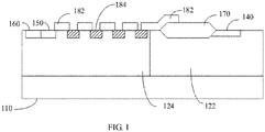
- FIG. 1 is a schematic view of a laterally diffused metal-oxide-semiconductor field-effect transistor according to one embodiment, which includes a P-type substrate 110, an N well 122, a P well 124, an N+ source 150 and a P+ body region 160 located in the P well 124, an N+ drain 140 in the N well 122, a gate doped region 184 in the P well 124, and a field oxide region 170 located between the source 150 and the drain 140.
- a polysilicon gate 182 has a multi-segments structure. A segment of the polysilicon gate 182 which is closest to the drain 140 extends to the field oxide region 170 to serve as a polycrystalline field plate.
- a first-conductivity type is N-type
- a second-conductivity type is P-type
- the first-conductivity type may be P-type
- the second-conductivity type is N-type
- the aforementioned laterally diffused metal-oxide-semiconductor field-effect transistor When the aforementioned laterally diffused metal-oxide-semiconductor field-effect transistor is in an on-state, electrons are implanted from the source 150 into a channel below the gate (a sub-channel below the leftmost segment of the polysilicon gate 182 in FIG. 1 ). Due to the potential difference between the gate and source 150, a high electric field is formed to accelerate the channel electrons to enter the leftmost one of the gate doped regions 184 in FIG. 1 . Afterwards, the electrons continue to move towards the drain 140 and enter the second sub-channel (the channel below the second segment of the polysilicon gate 182 from the left in FIG. 1 ), and are likewise accelerated by the gate doped region 184 on the right side of the channel. Similarly, the electrons are continuously accelerated between the adjacent two gate doped regions 184 during the movement from the source 150 towards the drain 130.
- LDMOSFET further includes a metal wiring layer.
- metal electrodes are provided in a gap between two segments of the polysilicon gate 182 above each of the gate doped regions 184 to form the metal wiring layer.
- Each of the gate doped regions 184 is electrically coupled to the segment of the polysilicon gate 182 on the left side thereof via the metal wiring layer (not shown in FIG. 1 ), thus ensuring that the sub-channel formed by each segment of the polysilicon gates 182 operates in a saturation region, so as to provide a high carrier mobility under high electric field.
- More gate doped regions 184 can be provided to help to further reduce the on-resistance.
- the device width is constant, the more gate doping regions 184 are provided in a width direction, the smaller width and the interval of each of the gate doping regions 184.
- the doped regions 184 separated from each other in the design may be connected with each other in one piece during manufacturing, which may lose the effect of RESURF and have an adverse effect on the breakdown voltage BV of the device. Therefore, in one embodiment, the LDMOSFET is provided with 3 to 5 sets of the gate doped regions 184 in a connection direction between the source and the drain. In the illustrated embodiment, referring to FIG. 1 , four sets of the gate doped regions 184 are provided.
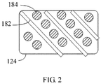
- each set of the gate doped regions 184 includes a plurality of gate doped regions. Referring to FIG. 2 , each of the gate doped regions 184 in each set is arranged in a direction perpendicular to a channel current between the source 150 and the drain 140.
- FIG. 2 is a top plan view showing that the direction of the channel current between the source 150 and the drain 140 (i.e., the connection direction between the source 150 and the drain 140) is the X axis, and the height direction of the device is the Z axis to establish a space rectangular coordinate system.
- the plurality of gate doping regions 184 are provided not only in the X-axis direction but also in the Y-axis direction (or in a direction at a certain angle to the Y-axis on the XY plane).
- this configuration is more conducive to achieving charge balance between the P-well 124 and the gate doped region 184, while improving the redundancy of the implantation process, such that a small deviation of implantation dose does not cause a large withstand voltage fluctuation.
- the structure can also ensure a maximum current path and reduce the on-resistance of the P well 124.
- these gate doped regions 184 can assist in depleting the P well 124, thereby improving the withstand voltage of the device.
- an interval between the adjacent gate doped regions 184 in the connection direction between the source 150 and the drain 140 is less than or equal to 0.8 ⁇ m.
- the gate doped regions 184 are not connected with each other during manufacturing, and a better effect of reducing the on-resistance can also be obtained.
- each of the gate doped regions 184 has a width (i.e., a dimension in the connection direction between the source 150 and the drain 140) of 1 ⁇ m to 2.5 ⁇ m.
- the gate doped region 184 has an implantation dose of 0.8 E13/cm 2 to 1.5 E13/cm 2 , a junction depth of about 0.8 ⁇ m, and a peak concentration of 1.0 E13/cm 2 to 2.0 E17/cm 3 . Under the aforementioned conditions, the device can reach a minimum breakdown voltage of approximately 600 V.
- the number of channel electrons of the aforementioned LDMOSFET is increased, and electrons are accelerated for several times during flowing from the source to the drain, which is equivalent to an increase in the channel electric field and the channel current. Therefore, the channel resistance is reduced, thereby reducing the on-resistance. Meanwhile, the reduction of the channel resistance helps to improve the optimization space of a drift region, and the concentration of the drift region can be further reduced, thereby improving the withstand voltage (breakdown voltage) of the device. Alternatively, the length of the drift region can be further shortened while keeping the withstand voltage constant, thereby reducing the device cost.
Landscapes
- Insulated Gate Type Field-Effect Transistor (AREA)
Applications Claiming Priority (2)
| Application Number | Priority Date | Filing Date | Title |
|---|---|---|---|
| CN201510864548.5A CN106816468B (zh) | 2015-11-30 | 2015-11-30 | 具有resurf结构的横向扩散金属氧化物半导体场效应管 |
| PCT/CN2016/096730 WO2017092419A1 (zh) | 2015-11-30 | 2016-08-25 | 横向扩散金属氧化物半导体场效应管 |
Publications (3)
| Publication Number | Publication Date |
|---|---|
| EP3385993A1 true EP3385993A1 (de) | 2018-10-10 |
| EP3385993A4 EP3385993A4 (de) | 2019-07-24 |
| EP3385993B1 EP3385993B1 (de) | 2022-11-02 |
Family
ID=58796181
Family Applications (1)
| Application Number | Title | Priority Date | Filing Date |
|---|---|---|---|
| EP16869730.8A Active EP3385993B1 (de) | 2015-11-30 | 2016-08-25 | Lateraler diffundierter metalloxid-halbleiter-feldeffekttransistor |
Country Status (6)
| Country | Link |
|---|---|
| US (1) | US10505036B2 (de) |
| EP (1) | EP3385993B1 (de) |
| JP (1) | JP6615348B2 (de) |
| KR (1) | KR102144625B1 (de) |
| CN (1) | CN106816468B (de) |
| WO (1) | WO2017092419A1 (de) |
Families Citing this family (9)
| Publication number | Priority date | Publication date | Assignee | Title |
|---|---|---|---|---|
| CN106158956B (zh) * | 2015-04-08 | 2020-02-11 | 无锡华润上华科技有限公司 | 具有resurf结构的ldmosfet及其制造方法 |
| CN106483758B (zh) | 2015-09-02 | 2019-08-20 | 无锡华润上华科技有限公司 | 光学邻近效应修正方法和系统 |
| CN106653842B (zh) | 2015-10-28 | 2019-05-17 | 无锡华润上华科技有限公司 | 一种具有静电释放保护结构的半导体器件 |
| CN107465983B (zh) | 2016-06-03 | 2021-06-04 | 无锡华润上华科技有限公司 | Mems麦克风及其制备方法 |
| CN110518056B (zh) * | 2019-08-02 | 2021-06-01 | 无锡华润上华科技有限公司 | 横向扩散金属氧化物半导体器件及其制造方法 |
| CN110534514B (zh) * | 2019-09-05 | 2022-01-25 | 电子科技大学 | 一种横向高压功率半导体器件的槽型终端结构 |
| CN113130647B (zh) * | 2019-12-30 | 2023-01-13 | 比亚迪半导体股份有限公司 | 碳化硅器件及其制备方法和半导体器件 |
| JP7815134B2 (ja) * | 2020-10-29 | 2026-02-17 | ローム株式会社 | 半導体装置 |
| CN114784106A (zh) * | 2022-03-31 | 2022-07-22 | 西安电子科技大学 | 一种具有额外电极的折叠硅ldmos及其制作方法 |
Family Cites Families (32)
| Publication number | Priority date | Publication date | Assignee | Title |
|---|---|---|---|---|
| JP3435294B2 (ja) * | 1996-09-11 | 2003-08-11 | 株式会社東芝 | Mosゲート半導体装置 |
| US6873011B1 (en) | 2004-02-24 | 2005-03-29 | System General Corp. | High voltage and low on-resistance LDMOS transistor having equalized capacitance |
| WO2008076961A1 (en) * | 2006-12-15 | 2008-06-26 | Board Of Regents, The University Of Texas System | Nitric oxide increases switching of t cells into t regulatory cells |
| US8174069B2 (en) * | 2008-08-05 | 2012-05-08 | Cambridge Semiconductor Limited | Power semiconductor device and a method of forming a power semiconductor device |
| KR101049876B1 (ko) | 2008-11-19 | 2011-07-19 | 주식회사 동부하이텍 | 횡형 디모스 소자 및 그의 제조 방법 |
| US8319283B2 (en) * | 2009-05-29 | 2012-11-27 | Freescale Semiconductor, Inc. | Laterally diffused metal oxide semiconductor (LDMOS) device with multiple gates and doped regions |
| US20150061008A1 (en) * | 2009-11-13 | 2015-03-05 | Maxim Integrated Products, Inc. | Ldmosfet having a bridge region formed between two gate electrodes |
| US8704312B2 (en) * | 2010-01-05 | 2014-04-22 | Taiwan Semiconductor Manufacturing Company, Ltd. | High voltage devices and methods of forming the high voltage devices |
| CN101969074B (zh) * | 2010-10-28 | 2012-07-04 | 电子科技大学 | 一种高压ldmos器件 |
| US8610206B2 (en) | 2011-02-18 | 2013-12-17 | Macronix International Co., Ltd. | Split-gate lateral diffused metal oxide semiconductor device |
| CN104332494B (zh) | 2013-07-22 | 2018-09-21 | 无锡华润上华科技有限公司 | 一种绝缘栅双极晶体管及其制造方法 |
| CN104347401B (zh) | 2013-07-29 | 2017-05-10 | 无锡华润上华半导体有限公司 | 一种绝缘栅双极性晶体管的制造方法 |
| CN104425245B (zh) | 2013-08-23 | 2017-11-07 | 无锡华润上华科技有限公司 | 反向导通绝缘栅双极型晶体管制造方法 |
| CN103594517A (zh) * | 2013-10-24 | 2014-02-19 | 中国科学院上海微系统与信息技术研究所 | 一种多栅soi-ldmos器件结构 |
| CN104701356B (zh) | 2013-12-06 | 2018-01-12 | 无锡华润上华科技有限公司 | 半导体器件及其制备方法 |
| CN104760925B (zh) | 2014-01-07 | 2016-05-25 | 无锡华润上华半导体有限公司 | 一种薄膜支撑梁的制作方法 |
| CN105097776B (zh) | 2014-04-29 | 2018-03-16 | 无锡华润上华科技有限公司 | 绝缘体上硅器件及其金属间介质层结构和制造方法 |
| CN105097795B (zh) | 2014-05-04 | 2018-03-16 | 无锡华润上华科技有限公司 | 具esd保护结构的半导体器件 |
| CN105092110A (zh) | 2014-05-06 | 2015-11-25 | 无锡华润上华半导体有限公司 | 压力传感器及其制作方法 |
| CN105095537B (zh) | 2014-05-08 | 2018-03-23 | 无锡华润上华科技有限公司 | 高压器件的仿真模型和高压器件仿真模型的建模方法 |
| CN105174203B (zh) | 2014-05-28 | 2016-09-28 | 无锡华润上华半导体有限公司 | 基于mems的传感器的制作方法 |
| CN105223781B (zh) | 2014-06-26 | 2017-06-23 | 无锡华润上华科技有限公司 | 一种步进式光刻机对位监控方法 |
| CN105226101B (zh) | 2014-06-30 | 2018-04-10 | 无锡华润上华科技有限公司 | 结型场效应晶体管及其制造方法 |
| CN105445529B (zh) | 2014-07-28 | 2018-06-15 | 无锡华润上华科技有限公司 | 具有时序控制功能的掉电检测电路 |
| CN105446404B (zh) | 2014-08-19 | 2017-08-08 | 无锡华润上华半导体有限公司 | 低压差线性稳压器电路、芯片和电子设备 |
| JP6534813B2 (ja) | 2015-01-08 | 2019-06-26 | ルネサスエレクトロニクス株式会社 | 半導体装置および半導体装置の製造方法 |
| CN105789306B (zh) | 2015-01-12 | 2020-12-08 | 台湾积体电路制造股份有限公司 | 半导体器件及其制造方法 |
| CN106158921B (zh) | 2015-04-10 | 2019-07-23 | 无锡华润上华科技有限公司 | 具resurf结构的横向扩散金属氧化物半导体场效应管 |
| CN106158957B (zh) | 2015-04-10 | 2019-05-17 | 无锡华润上华科技有限公司 | 横向扩散金属氧化物半导体场效应管及其制造方法 |
| CN106303867B (zh) | 2015-05-13 | 2019-02-01 | 无锡华润上华科技有限公司 | Mems麦克风 |
| CN106483758B (zh) | 2015-09-02 | 2019-08-20 | 无锡华润上华科技有限公司 | 光学邻近效应修正方法和系统 |
| CN106571370B (zh) | 2015-10-08 | 2019-12-10 | 无锡华润上华科技有限公司 | 基于soi工艺的介质电容 |
-
2015
- 2015-11-30 CN CN201510864548.5A patent/CN106816468B/zh active Active
-
2016
- 2016-08-25 KR KR1020187017322A patent/KR102144625B1/ko active Active
- 2016-08-25 US US15/779,666 patent/US10505036B2/en active Active
- 2016-08-25 JP JP2018527941A patent/JP6615348B2/ja active Active
- 2016-08-25 WO PCT/CN2016/096730 patent/WO2017092419A1/zh not_active Ceased
- 2016-08-25 EP EP16869730.8A patent/EP3385993B1/de active Active
Also Published As
| Publication number | Publication date |
|---|---|
| JP2018535559A (ja) | 2018-11-29 |
| KR20180083925A (ko) | 2018-07-23 |
| US10505036B2 (en) | 2019-12-10 |
| US20180342609A1 (en) | 2018-11-29 |
| JP6615348B2 (ja) | 2019-12-04 |
| EP3385993B1 (de) | 2022-11-02 |
| CN106816468B (zh) | 2020-07-10 |
| WO2017092419A1 (zh) | 2017-06-08 |
| EP3385993A4 (de) | 2019-07-24 |
| KR102144625B1 (ko) | 2020-08-14 |
| CN106816468A (zh) | 2017-06-09 |
Similar Documents
| Publication | Publication Date | Title |
|---|---|---|
| US10505036B2 (en) | Lateral diffused metal oxide semiconductor field effect transistor | |
| US7535057B2 (en) | DMOS transistor with a poly-filled deep trench for improved performance | |
| US10529849B2 (en) | High-voltage semiconductor device including a super-junction doped structure | |
| US9443973B2 (en) | Semiconductor device with charge compensation region underneath gate trench | |
| US9799764B2 (en) | Lateral power integrated devices having low on-resistance | |
| US9905687B1 (en) | Semiconductor device and method of making | |
| US11316021B2 (en) | High density power device with selectively shielded recessed field plate | |
| US10700193B2 (en) | Power device | |
| US7514743B2 (en) | DMOS transistor with floating poly-filled trench for improved performance through 3-D field shaping | |
| KR20090031548A (ko) | 소스-드레인간 직통 전류 경로를 갖는 횡형 트랜치 게이트 전계효과 트랜지스터 | |
| KR20140124950A (ko) | 반도체 전력소자 | |
| US12119377B2 (en) | SiC devices with shielding structure | |
| US20230268433A1 (en) | Semiconductor device | |
| US10199495B2 (en) | Laterally diffused metal-oxide semiconductor field-effect transistor | |
| US9520493B1 (en) | High voltage integrated circuits having improved on-resistance value and improved breakdown voltage | |
| US11049938B2 (en) | P-type lateral double diffused MOS transistor and method of manufacturing the same | |
| CN106887451B (zh) | 超结器件及其制造方法 | |
| CN114402438B (zh) | 半导体设备以及用于制造半导体设备的方法 | |
| KR102385949B1 (ko) | 낮은 온 저항을 갖는 수평형 전력용 집적 소자 | |
| EP4258361A2 (de) | Vertikal abgeschirmter gate-akkumulationsfeldeffekttransistor | |
| EP3671858A1 (de) | Ldmos mit vergrabener schiene als zusätzliches gate | |
| KR20190076622A (ko) | 이너 웰을 가진 슈퍼 정션 트랜지스터 | |
| KR20140029951A (ko) | 반도체 장치 |
Legal Events
| Date | Code | Title | Description |
|---|---|---|---|
| STAA | Information on the status of an ep patent application or granted ep patent |
Free format text: STATUS: THE INTERNATIONAL PUBLICATION HAS BEEN MADE |
|
| PUAI | Public reference made under article 153(3) epc to a published international application that has entered the european phase |
Free format text: ORIGINAL CODE: 0009012 |
|
| STAA | Information on the status of an ep patent application or granted ep patent |
Free format text: STATUS: REQUEST FOR EXAMINATION WAS MADE |
|
| 17P | Request for examination filed |
Effective date: 20180702 |
|
| AK | Designated contracting states |
Kind code of ref document: A1 Designated state(s): AL AT BE BG CH CY CZ DE DK EE ES FI FR GB GR HR HU IE IS IT LI LT LU LV MC MK MT NL NO PL PT RO RS SE SI SK SM TR |
|
| AX | Request for extension of the european patent |
Extension state: BA ME |
|
| DAV | Request for validation of the european patent (deleted) | ||
| DAX | Request for extension of the european patent (deleted) | ||
| A4 | Supplementary search report drawn up and despatched |
Effective date: 20190625 |
|
| RIC1 | Information provided on ipc code assigned before grant |
Ipc: H01L 29/423 20060101ALI20190618BHEP Ipc: H01L 29/40 20060101ALI20190618BHEP Ipc: H01L 29/78 20060101AFI20190618BHEP Ipc: H01L 29/06 20060101ALI20190618BHEP |
|
| STAA | Information on the status of an ep patent application or granted ep patent |
Free format text: STATUS: EXAMINATION IS IN PROGRESS |
|
| 17Q | First examination report despatched |
Effective date: 20210310 |
|
| GRAP | Despatch of communication of intention to grant a patent |
Free format text: ORIGINAL CODE: EPIDOSNIGR1 |
|
| STAA | Information on the status of an ep patent application or granted ep patent |
Free format text: STATUS: GRANT OF PATENT IS INTENDED |
|
| INTG | Intention to grant announced |
Effective date: 20220519 |
|
| GRAS | Grant fee paid |
Free format text: ORIGINAL CODE: EPIDOSNIGR3 |
|
| GRAA | (expected) grant |
Free format text: ORIGINAL CODE: 0009210 |
|
| STAA | Information on the status of an ep patent application or granted ep patent |
Free format text: STATUS: THE PATENT HAS BEEN GRANTED |
|
| AK | Designated contracting states |
Kind code of ref document: B1 Designated state(s): AL AT BE BG CH CY CZ DE DK EE ES FI FR GB GR HR HU IE IS IT LI LT LU LV MC MK MT NL NO PL PT RO RS SE SI SK SM TR |
|
| REG | Reference to a national code |
Ref country code: GB Ref legal event code: FG4D |
|
| REG | Reference to a national code |
Ref country code: CH Ref legal event code: EP Ref country code: AT Ref legal event code: REF Ref document number: 1529402 Country of ref document: AT Kind code of ref document: T Effective date: 20221115 |
|
| REG | Reference to a national code |
Ref country code: DE Ref legal event code: R096 Ref document number: 602016076131 Country of ref document: DE |
|
| REG | Reference to a national code |
Ref country code: IE Ref legal event code: FG4D |
|
| REG | Reference to a national code |
Ref country code: NL Ref legal event code: FP |
|
| REG | Reference to a national code |
Ref country code: LT Ref legal event code: MG9D |
|
| REG | Reference to a national code |
Ref country code: AT Ref legal event code: MK05 Ref document number: 1529402 Country of ref document: AT Kind code of ref document: T Effective date: 20221102 |
|
| PG25 | Lapsed in a contracting state [announced via postgrant information from national office to epo] |
Ref country code: SE Free format text: LAPSE BECAUSE OF FAILURE TO SUBMIT A TRANSLATION OF THE DESCRIPTION OR TO PAY THE FEE WITHIN THE PRESCRIBED TIME-LIMIT Effective date: 20221102 Ref country code: PT Free format text: LAPSE BECAUSE OF FAILURE TO SUBMIT A TRANSLATION OF THE DESCRIPTION OR TO PAY THE FEE WITHIN THE PRESCRIBED TIME-LIMIT Effective date: 20230302 Ref country code: NO Free format text: LAPSE BECAUSE OF FAILURE TO SUBMIT A TRANSLATION OF THE DESCRIPTION OR TO PAY THE FEE WITHIN THE PRESCRIBED TIME-LIMIT Effective date: 20230202 Ref country code: LT Free format text: LAPSE BECAUSE OF FAILURE TO SUBMIT A TRANSLATION OF THE DESCRIPTION OR TO PAY THE FEE WITHIN THE PRESCRIBED TIME-LIMIT Effective date: 20221102 Ref country code: FI Free format text: LAPSE BECAUSE OF FAILURE TO SUBMIT A TRANSLATION OF THE DESCRIPTION OR TO PAY THE FEE WITHIN THE PRESCRIBED TIME-LIMIT Effective date: 20221102 Ref country code: ES Free format text: LAPSE BECAUSE OF FAILURE TO SUBMIT A TRANSLATION OF THE DESCRIPTION OR TO PAY THE FEE WITHIN THE PRESCRIBED TIME-LIMIT Effective date: 20221102 Ref country code: AT Free format text: LAPSE BECAUSE OF FAILURE TO SUBMIT A TRANSLATION OF THE DESCRIPTION OR TO PAY THE FEE WITHIN THE PRESCRIBED TIME-LIMIT Effective date: 20221102 |
|
| PG25 | Lapsed in a contracting state [announced via postgrant information from national office to epo] |
Ref country code: RS Free format text: LAPSE BECAUSE OF FAILURE TO SUBMIT A TRANSLATION OF THE DESCRIPTION OR TO PAY THE FEE WITHIN THE PRESCRIBED TIME-LIMIT Effective date: 20221102 Ref country code: PL Free format text: LAPSE BECAUSE OF FAILURE TO SUBMIT A TRANSLATION OF THE DESCRIPTION OR TO PAY THE FEE WITHIN THE PRESCRIBED TIME-LIMIT Effective date: 20221102 Ref country code: LV Free format text: LAPSE BECAUSE OF FAILURE TO SUBMIT A TRANSLATION OF THE DESCRIPTION OR TO PAY THE FEE WITHIN THE PRESCRIBED TIME-LIMIT Effective date: 20221102 Ref country code: IS Free format text: LAPSE BECAUSE OF FAILURE TO SUBMIT A TRANSLATION OF THE DESCRIPTION OR TO PAY THE FEE WITHIN THE PRESCRIBED TIME-LIMIT Effective date: 20230302 Ref country code: HR Free format text: LAPSE BECAUSE OF FAILURE TO SUBMIT A TRANSLATION OF THE DESCRIPTION OR TO PAY THE FEE WITHIN THE PRESCRIBED TIME-LIMIT Effective date: 20221102 Ref country code: GR Free format text: LAPSE BECAUSE OF FAILURE TO SUBMIT A TRANSLATION OF THE DESCRIPTION OR TO PAY THE FEE WITHIN THE PRESCRIBED TIME-LIMIT Effective date: 20230203 |
|
| PG25 | Lapsed in a contracting state [announced via postgrant information from national office to epo] |
Ref country code: SM Free format text: LAPSE BECAUSE OF FAILURE TO SUBMIT A TRANSLATION OF THE DESCRIPTION OR TO PAY THE FEE WITHIN THE PRESCRIBED TIME-LIMIT Effective date: 20221102 Ref country code: RO Free format text: LAPSE BECAUSE OF FAILURE TO SUBMIT A TRANSLATION OF THE DESCRIPTION OR TO PAY THE FEE WITHIN THE PRESCRIBED TIME-LIMIT Effective date: 20221102 Ref country code: EE Free format text: LAPSE BECAUSE OF FAILURE TO SUBMIT A TRANSLATION OF THE DESCRIPTION OR TO PAY THE FEE WITHIN THE PRESCRIBED TIME-LIMIT Effective date: 20221102 Ref country code: DK Free format text: LAPSE BECAUSE OF FAILURE TO SUBMIT A TRANSLATION OF THE DESCRIPTION OR TO PAY THE FEE WITHIN THE PRESCRIBED TIME-LIMIT Effective date: 20221102 Ref country code: CZ Free format text: LAPSE BECAUSE OF FAILURE TO SUBMIT A TRANSLATION OF THE DESCRIPTION OR TO PAY THE FEE WITHIN THE PRESCRIBED TIME-LIMIT Effective date: 20221102 |
|
| REG | Reference to a national code |
Ref country code: DE Ref legal event code: R097 Ref document number: 602016076131 Country of ref document: DE |
|
| PG25 | Lapsed in a contracting state [announced via postgrant information from national office to epo] |
Ref country code: SK Free format text: LAPSE BECAUSE OF FAILURE TO SUBMIT A TRANSLATION OF THE DESCRIPTION OR TO PAY THE FEE WITHIN THE PRESCRIBED TIME-LIMIT Effective date: 20221102 Ref country code: AL Free format text: LAPSE BECAUSE OF FAILURE TO SUBMIT A TRANSLATION OF THE DESCRIPTION OR TO PAY THE FEE WITHIN THE PRESCRIBED TIME-LIMIT Effective date: 20221102 |
|
| PLBE | No opposition filed within time limit |
Free format text: ORIGINAL CODE: 0009261 |
|
| STAA | Information on the status of an ep patent application or granted ep patent |
Free format text: STATUS: NO OPPOSITION FILED WITHIN TIME LIMIT |
|
| 26N | No opposition filed |
Effective date: 20230803 |
|
| PG25 | Lapsed in a contracting state [announced via postgrant information from national office to epo] |
Ref country code: SI Free format text: LAPSE BECAUSE OF FAILURE TO SUBMIT A TRANSLATION OF THE DESCRIPTION OR TO PAY THE FEE WITHIN THE PRESCRIBED TIME-LIMIT Effective date: 20221102 |
|
| PG25 | Lapsed in a contracting state [announced via postgrant information from national office to epo] |
Ref country code: MC Free format text: LAPSE BECAUSE OF FAILURE TO SUBMIT A TRANSLATION OF THE DESCRIPTION OR TO PAY THE FEE WITHIN THE PRESCRIBED TIME-LIMIT Effective date: 20221102 |
|
| REG | Reference to a national code |
Ref country code: CH Ref legal event code: PL |
|
| PG25 | Lapsed in a contracting state [announced via postgrant information from national office to epo] |
Ref country code: MC Free format text: LAPSE BECAUSE OF FAILURE TO SUBMIT A TRANSLATION OF THE DESCRIPTION OR TO PAY THE FEE WITHIN THE PRESCRIBED TIME-LIMIT Effective date: 20221102 |
|
| PG25 | Lapsed in a contracting state [announced via postgrant information from national office to epo] |
Ref country code: LU Free format text: LAPSE BECAUSE OF NON-PAYMENT OF DUE FEES Effective date: 20230825 |
|
| PG25 | Lapsed in a contracting state [announced via postgrant information from national office to epo] |
Ref country code: LU Free format text: LAPSE BECAUSE OF NON-PAYMENT OF DUE FEES Effective date: 20230825 Ref country code: CH Free format text: LAPSE BECAUSE OF NON-PAYMENT OF DUE FEES Effective date: 20230831 |
|
| REG | Reference to a national code |
Ref country code: BE Ref legal event code: MM Effective date: 20230831 |
|
| REG | Reference to a national code |
Ref country code: IE Ref legal event code: MM4A |
|
| PG25 | Lapsed in a contracting state [announced via postgrant information from national office to epo] |
Ref country code: IT Free format text: LAPSE BECAUSE OF FAILURE TO SUBMIT A TRANSLATION OF THE DESCRIPTION OR TO PAY THE FEE WITHIN THE PRESCRIBED TIME-LIMIT Effective date: 20221102 |
|
| PG25 | Lapsed in a contracting state [announced via postgrant information from national office to epo] |
Ref country code: IE Free format text: LAPSE BECAUSE OF NON-PAYMENT OF DUE FEES Effective date: 20230825 |
|
| PG25 | Lapsed in a contracting state [announced via postgrant information from national office to epo] |
Ref country code: IE Free format text: LAPSE BECAUSE OF NON-PAYMENT OF DUE FEES Effective date: 20230825 |
|
| PG25 | Lapsed in a contracting state [announced via postgrant information from national office to epo] |
Ref country code: BE Free format text: LAPSE BECAUSE OF NON-PAYMENT OF DUE FEES Effective date: 20230831 |
|
| PG25 | Lapsed in a contracting state [announced via postgrant information from national office to epo] |
Ref country code: BG Free format text: LAPSE BECAUSE OF FAILURE TO SUBMIT A TRANSLATION OF THE DESCRIPTION OR TO PAY THE FEE WITHIN THE PRESCRIBED TIME-LIMIT Effective date: 20221102 |
|
| REG | Reference to a national code |
Ref country code: DE Ref legal event code: R079 Ref document number: 602016076131 Country of ref document: DE Free format text: PREVIOUS MAIN CLASS: H01L0029780000 Ipc: H10D0030600000 |
|
| PG25 | Lapsed in a contracting state [announced via postgrant information from national office to epo] |
Ref country code: BG Free format text: LAPSE BECAUSE OF FAILURE TO SUBMIT A TRANSLATION OF THE DESCRIPTION OR TO PAY THE FEE WITHIN THE PRESCRIBED TIME-LIMIT Effective date: 20221102 |
|
| PG25 | Lapsed in a contracting state [announced via postgrant information from national office to epo] |
Ref country code: CY Free format text: LAPSE BECAUSE OF FAILURE TO SUBMIT A TRANSLATION OF THE DESCRIPTION OR TO PAY THE FEE WITHIN THE PRESCRIBED TIME-LIMIT; INVALID AB INITIO Effective date: 20160825 |
|
| PG25 | Lapsed in a contracting state [announced via postgrant information from national office to epo] |
Ref country code: HU Free format text: LAPSE BECAUSE OF FAILURE TO SUBMIT A TRANSLATION OF THE DESCRIPTION OR TO PAY THE FEE WITHIN THE PRESCRIBED TIME-LIMIT; INVALID AB INITIO Effective date: 20160825 |
|
| PGFP | Annual fee paid to national office [announced via postgrant information from national office to epo] |
Ref country code: NL Payment date: 20250821 Year of fee payment: 10 |
|
| PGFP | Annual fee paid to national office [announced via postgrant information from national office to epo] |
Ref country code: DE Payment date: 20250820 Year of fee payment: 10 |
|
| PGFP | Annual fee paid to national office [announced via postgrant information from national office to epo] |
Ref country code: GB Payment date: 20250821 Year of fee payment: 10 |
|
| PGFP | Annual fee paid to national office [announced via postgrant information from national office to epo] |
Ref country code: FR Payment date: 20250828 Year of fee payment: 10 |
|
| PG25 | Lapsed in a contracting state [announced via postgrant information from national office to epo] |
Ref country code: TR Free format text: LAPSE BECAUSE OF FAILURE TO SUBMIT A TRANSLATION OF THE DESCRIPTION OR TO PAY THE FEE WITHIN THE PRESCRIBED TIME-LIMIT Effective date: 20221102 |