EP3384497B1 - Niedrigleistungsleseverstärker für flash-speichersystem - Google Patents
Niedrigleistungsleseverstärker für flash-speichersystem Download PDFInfo
- Publication number
- EP3384497B1 EP3384497B1 EP16882287.2A EP16882287A EP3384497B1 EP 3384497 B1 EP3384497 B1 EP 3384497B1 EP 16882287 A EP16882287 A EP 16882287A EP 3384497 B1 EP3384497 B1 EP 3384497B1
- Authority
- EP
- European Patent Office
- Prior art keywords
- terminal
- output
- flash memory
- coupled
- gate
- Prior art date
- Legal status (The legal status is an assumption and is not a legal conclusion. Google has not performed a legal analysis and makes no representation as to the accuracy of the status listed.)
- Active
Links
Images



Classifications
-
- G—PHYSICS
- G11—INFORMATION STORAGE
- G11C—STATIC STORES
- G11C16/00—Erasable programmable read-only memories
- G11C16/02—Erasable programmable read-only memories electrically programmable
- G11C16/06—Auxiliary circuits, e.g. for writing into memory
- G11C16/24—Bit-line control circuits
-
- G—PHYSICS
- G11—INFORMATION STORAGE
- G11C—STATIC STORES
- G11C16/00—Erasable programmable read-only memories
- G11C16/02—Erasable programmable read-only memories electrically programmable
- G11C16/06—Auxiliary circuits, e.g. for writing into memory
- G11C16/26—Sensing or reading circuits; Data output circuits
-
- G—PHYSICS
- G11—INFORMATION STORAGE
- G11C—STATIC STORES
- G11C16/00—Erasable programmable read-only memories
- G11C16/02—Erasable programmable read-only memories electrically programmable
- G11C16/06—Auxiliary circuits, e.g. for writing into memory
- G11C16/26—Sensing or reading circuits; Data output circuits
- G11C16/28—Sensing or reading circuits; Data output circuits using differential sensing or reference cells, e.g. dummy cells
-
- G—PHYSICS
- G11—INFORMATION STORAGE
- G11C—STATIC STORES
- G11C29/00—Checking stores for correct operation ; Subsequent repair; Testing stores during standby or offline operation
- G11C29/02—Detection or location of defective auxiliary circuits, e.g. defective refresh counters
- G11C29/022—Detection or location of defective auxiliary circuits, e.g. defective refresh counters in I/O circuitry
-
- G—PHYSICS
- G11—INFORMATION STORAGE
- G11C—STATIC STORES
- G11C29/00—Checking stores for correct operation ; Subsequent repair; Testing stores during standby or offline operation
- G11C29/04—Detection or location of defective memory elements, e.g. cell constructio details, timing of test signals
- G11C29/50—Marginal testing, e.g. race, voltage or current testing
-
- G—PHYSICS
- G11—INFORMATION STORAGE
- G11C—STATIC STORES
- G11C7/00—Arrangements for writing information into, or reading information out from, a digital store
- G11C7/06—Sense amplifiers; Associated circuits, e.g. timing or triggering circuits
- G11C7/062—Differential amplifiers of non-latching type, e.g. comparators, long-tailed pairs
-
- G—PHYSICS
- G11—INFORMATION STORAGE
- G11C—STATIC STORES
- G11C7/00—Arrangements for writing information into, or reading information out from, a digital store
- G11C7/06—Sense amplifiers; Associated circuits, e.g. timing or triggering circuits
- G11C7/067—Single-ended amplifiers
-
- G—PHYSICS
- G11—INFORMATION STORAGE
- G11C—STATIC STORES
- G11C7/00—Arrangements for writing information into, or reading information out from, a digital store
- G11C7/14—Dummy cell management; Sense reference voltage generators
-
- G—PHYSICS
- G11—INFORMATION STORAGE
- G11C—STATIC STORES
- G11C16/00—Erasable programmable read-only memories
- G11C16/02—Erasable programmable read-only memories electrically programmable
- G11C16/04—Erasable programmable read-only memories electrically programmable using variable threshold transistors, e.g. FAMOS
- G11C16/0483—Erasable programmable read-only memories electrically programmable using variable threshold transistors, e.g. FAMOS comprising cells having several storage transistors connected in series
-
- G—PHYSICS
- G11—INFORMATION STORAGE
- G11C—STATIC STORES
- G11C16/00—Erasable programmable read-only memories
- G11C16/02—Erasable programmable read-only memories electrically programmable
- G11C16/06—Auxiliary circuits, e.g. for writing into memory
- G11C16/32—Timing circuits
-
- G—PHYSICS
- G11—INFORMATION STORAGE
- G11C—STATIC STORES
- G11C29/00—Checking stores for correct operation ; Subsequent repair; Testing stores during standby or offline operation
- G11C29/04—Detection or location of defective memory elements, e.g. cell constructio details, timing of test signals
- G11C29/08—Functional testing, e.g. testing during refresh, power-on self testing [POST] or distributed testing
- G11C29/12—Built-in arrangements for testing, e.g. built-in self testing [BIST] or interconnection details
- G11C2029/1204—Bit line control
-
- G—PHYSICS
- G11—INFORMATION STORAGE
- G11C—STATIC STORES
- G11C29/00—Checking stores for correct operation ; Subsequent repair; Testing stores during standby or offline operation
- G11C29/04—Detection or location of defective memory elements, e.g. cell constructio details, timing of test signals
- G11C29/50—Marginal testing, e.g. race, voltage or current testing
- G11C2029/5006—Current
-
- G—PHYSICS
- G11—INFORMATION STORAGE
- G11C—STATIC STORES
- G11C2207/00—Indexing scheme relating to arrangements for writing information into, or reading information out from, a digital store
- G11C2207/22—Control and timing of internal memory operations
- G11C2207/2254—Calibration
Definitions
- US 2014/043886 A1 discloses a digital memory element that has a sense circuit latch to read the value stored in a bit cell. Before addressing a word line, the bit lines are precharged.
- US 2012/1 551 77 A1 discloses structures and methods of reading out semiconductor NonVolatile Memory (NVM) using referencing cells.
- NVM NonVolatile Memory
- US 6 272 062 B1 discloses a semiconductor memory device that includes a plurality of memory cells arranged in at least two groups; at least one sense amplifier; a first and a second multiplexer; and at least one programmable control device.
- US 6 055 200 A discloses variable test voltage circuits and methods provided for ferroelectric memory devices.
- the ferroelectric memory devices include a first bit line, a word line, a nonvolatile memory cell at an intersection of the first bit line and the word line, a second bit line corresponding to the first bit line and a sense amplifier connected between the first and second bit lines to sense a voltage difference between the first and second bit lines.
- US 2013/235672 A1 discloses a memory array for storing a plurality of data bits.
- the memory array has flash memory cells, ROM memory cells addressing circuitry.
- Flash memory systems are well-known.
- a sense amplifier is used to read data from a flash memory cell.
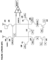
- Figure 1 depicts a prior art sense amplifier 100.
- Sense amplifier 100 comprises selected flash memory cell 102, which is the cell to be read.
- Sense amplifier 100 also comprises reference flash memory cell 122, against which selected flash memory cell 102 is compared.
- PMOS transistors 104, 106, 124, and 126 and NMOS transistors 108, 110, 112, 128, and 130 are arranged as shown.
- PMOS transistor 104 is controlled by CASREF (column address strobe reference)
- PMOS 106 is controlled by SEN_B (sense amplifier enable, active low)
- NMOS transistors 108, 112, and 128 are controlled by ATD (address transition detection, which detects a change in the received address)
- NMOS transistors 110 and 130 are controlled by YMUX (Y multiplexor) which activates a BL (bit line).
- Selected flash memory cell 102 receives WL (word line) and SL (source line)
- reference memory cell 122 receives SL (source line).
- Comparator 130 receives two inputs that are directly related to the current drawn by selected flash memory cell 102 and reference memory cell 122, and the output SOUT is directly indicative of the data value stored in selected flash memory cell 102.
- reference memory cell 122 and its associated circuitry typically are provided in a separate read bank than the read bank in which selected memory cell 102 is located, which requires a large die area and more power consumption for additional Y-decoding.
- the CASREF signal also is sensitive to noise, and the CASREF circuit also consumes significant standby current.
- What is needed is an improved sense amplifier design for a flash memory system that consumes less power than prior art sense amplifier solutions. What is further needed is an embodiment of a sense amplifier that does not require a separate read bank of memory cells. What is further needed is a sense amplifier that can accurately detect small differences in current drawn by selected flash memory cell 102 and reference memory cell 122, as might be required during a Margin0/1 mode.
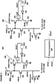
- FIG. 2 depicts sense amplifier 200.
- Sense amplifier 200 comprises reference circuit 280 and read circuit 290.
- Reference circuit 280 comprises reference memory cell 206, NMOS transistors 202, 204, and 220, PMOS transistor 212, reference bit line 208, level shifter 214, inverter 218, and NOR gate 216, all configured as shown.
- NMOS transistor 202 is controlled by ATD (address transition detection)
- NMOS transistor 204 is controlled by YMUX (Y multiplexor)
- NMOS transistor 220 is controlled by a BIAS signal.
- NOR gate 216 receives ATD as one of its inputs.
- Read circuit 290 comprises selected memory cell 236, NMOS transistors 232, 234, and 250, PMOS transistor 242, bit line 238, level shifter 244, inverter 248, and NOR gate 246, all configured as shown.
- NMOS transistor 232 is controlled by ATD (address transition detection)
- NMOS transistor 234 is controlled by YMUX (Y multiplexor)
- NMOS transistor 250 is controlled by a BIAS signal.
- NOR gate 246 receives ATD as one of its inputs.
- reference circuit 280 and read circuit 290 are identical, except that reference circuit 280 comprises reference memory cell 206, and read circuit 290 comprises selected memory cell 236.
- sense amplifier 200 works as follows. Prior to a read operation, the BIAS signal is high, which pulls the voltage at the output of inverters 218 and 248 to ground through NMOS transistors 220 and 250, which causes ROUT and SOUT to be high. At the beginning of a read operation, ATD goes high, which signifies a detection in the change of the address received by the memory system, which coincides with the beginning of a read operation.
- NMOS transistors 202 and 232 are turned on, as are NMOS transistors 204 and 234 by YMUX. This allows reference cell 206 and selected memory cell 236 to draw current. Concurrently, reference bit line 208 and bit line 238 will begin charging.
- BIAS also goes low at the beginning of the read operation. At this stage, PMOS transistors 212 and 242 are off, as the voltage on its gate will be high.
- Reference bit line 208 will begin discharging through reference cell 206. As it does so, the voltage of reference bit line 208 will decrease, and at some point will drop low enough (below VREF) such that PMOS transistor 212 turns on. This causes ROUT to drop to low.
- bit line 238 also is discharging through selected memory cell 236. As it does so, the voltage of bit line 238 will decrease, and at some point will drop low enough (below VREF) such that PMOS transistor 242 turns on. This causes SOUT to drop to low. Once ROUT/SOUT drop to low, each sense amplifier has a local feedback (216, 218 or 246, 248) to cut off its bias current, which reduces the power consumption.
- SOUT and ROUT are input into timing comparison circuit 260, and the output is DOUT, which indicates the value stored in selected memory cell 236.
- FIG. 3A depicts a first embodiment of timing comparison circuit 260.
- timing comparison circuit 260 comprises flip-flop 310, with SOUT as the D input, ROUT as the active low clock CK, and DOUT as the output.
- SOUT goes low before SOUT
- DOUT will output a "0,” indicating that selected memory cell 236 is storing a "0.”
- ROUT goes low after SOUT
- DOUT will output a "1," indicating that selected memory cell 236 is storing a "1.”
- FIG. 3B depicts a second embodiment of timing comparison circuit 260.
- Timing comparison circuit 260 comprises inverters 320 and 322 and NAND gates 324 and 326 configured as shown, with SOUT and ROUT as inputs, and DOUT as the output.
- SOUT goes low before SOUT
- DOUT will output a "0,” indicating that selected memory cell 236 is storing a "0.”
- DOUT goes low after SOUT
- DOUT will output a "1," indicating that selected memory cell 236 is storing a "1.”
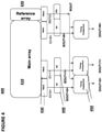
- FIG. 4 depicts flash memory system 400 utilizing sense amplifier 200 of Figures 2 , 3A, and 3B .
- Flash memory system 400 comprises main array 410 (comprising an array of flash memory cells, such as selected flash memory cell 236), reference array 420 (comprising an array of reference memory cells, such as reference memory cell 206), N+1 YMUX's 430, N+1 sense amplifiers 440 (each according to the design of sense amplifier 200), and N+1 timing comparison circuits 450 (each according the design of Figures 3A or 3B ).
- flash memory system 400 is capable of reading (sensing) N+1 bits at a time. Each bit is associated with one YMUX 430, one sense amplifier 440, and one timing comparison circuit 450 is used.
- Sense amplifier 200 consumes less power than prior art sense amplifier 100
- Sense amplifier 200 utilizes a small bias current during the sense operation instead of a larger reference current, and the small bias current is automatically cutoff after SOUT goes low.
- using the same type of YMUX for the reference cell and selected memory cell results in good transistor matching. In this embodiment, an extra read bank is not required.
- Flash memory system 500 comprises main array 410, reference array 420, YMUXs 430, sense amplifiers 440, reference sense amplifier 445, main array 460, dummy array 470, YMUXs 455, reference YMUX 480, and reference YMUX 490.
- a selected memory cell 236 is connected to one of the sense amplifiers 440. That same sense amplifier is connected to one or more bit lines coupled to memory cells in main array 460.
- a reference memory cell 206 is connected to reference sense amplifier 445, which is connected to one or more bit lines coupled to memory cells in dummy array 470.
- the number of bit lines and memory cells connected to a sense amplifier can change, which is a desirable feature for specific operation conditions (such as margin0/1 read modes).
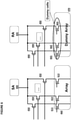
- sense amplifier 440 is selectively coupled to representative memory cells 611, 612, and 613 in main array 460 through YMUXs 450.
- Reference sense amplifier 445 is selectively coupled to representative dummy memory cells 661, 662, and 663 in dummy array 470 through RYMUXs 490.
- the number of bit lines and memory cells connected to a sense amplifier can change, which might is a desirable feature as operation conditions (such as temperature) changes.
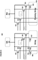
- FIG. 7 Another embodiment of the design of Figure 4 is shown in Figure 7 .
- sense amplifier 440 is selectively coupled to representative memory cells 611, 612, and 613 in main array 460 through YMUXs 450, respectively.
- Reference sense amplifier 445 is coupled in a fixed manner to dummy memory cells 661 in dummy array 470 through RYMUX 490. Thus, in this embodiment, reference sense amplifier 445 is coupled only to one reference memory cell and bit line.
- sense amplifier 440 is selectively coupled to representative memory cells 611, 612, and 613 in main array 460 through YMUXs 450.
- Sense amplifier 440 also is coupled to extra YMUX 801.
- Reference sense amplifier 445 is selectively coupled to dummy memory cell 851 through RYMUX 811.
- the embodiment of Figures 5 provides a new method of implementing a margin 0/1 test mode.
- the bit line loading on a sense amplifier is enlarged (from one bit line to N+1 bit lines) in order to distinguish very minor current differences for the 0/1 margin test mode.
- No current mirrors are used, which reduces both coupling and mismatching offsets of the prior art while using only a small area for the circuitry.
- references to the present invention herein are not intended to limit the scope of any claim or claim term, but instead merely make reference to one or more features that may be covered by one or more of the claims. Materials, processes and numerical examples described above are exemplary only, and should not be deemed to limit the claims. It should be noted that, as used herein, the terms “over” and “on” both inclusively include “directly on” (no intermediate materials, elements or space disposed there between) and “indirectly on” (intermediate materials, elements or space disposed there between). Likewise, the term “adjacent” includes “directly adjacent” (no intermediate materials, elements or space disposed there between) and “indirectly adjacent” (intermediate materials, elements or space disposed there between). For example, forming an element "over a substrate” can include forming the element directly on the substrate with no intermediate materials/elements there between, as well as forming the element indirectly on the substrate with one or more intermediate materials/elements there between.
Landscapes
- Read Only Memory (AREA)
Claims (6)
- Flash-Speichersystem (200), umfassend:eine erste Schaltung (290), umfassend:einen ersten NMOS-Transistor (232), umfassend einen ersten Anschluss, der an eine erste Spannungsquelle (VREF+ΔV) gekoppelt ist, einen zweiten Anschluss und ein Gate, das durch ein Adressübergangsdetektionssignal (ATD) gesteuert wird;einen zweiten NMOS-Transistor (234), umfassend einen ersten Anschluss, der an den zweiten Anschluss des ersten NMOS-Transistors gekoppelt ist, einen zweiten Anschluss und ein Gate, das durch ein Spaltenauswahlsignal (YMIIX) gesteuert wird;eine ausgewählte Flash-Speicherzelle (236), umfassend einen ersten Anschluss, der an eine erste Bitleitung (238) und den zweiten Anschluss des zweiten PMOS-Transistors (234) gekoppelt ist;einen ersten PMOS-Transistor (242), umfassend einen ersten Anschluss, der an eine zweite Spannungsquelle (VREF+Vthp) gekoppelt ist, einen zweiten Anschluss und ein Gate, das an den zweiten Anschluss des ersten NMOS-Transistors und den ersten Anschluss des zweiten NMOS-Transistors gekoppelt ist;einen ersten invertierenden Pegelumsetzer (244), umfassend einen Eingang, der an den zweiten Anschluss des ersten PMOS-Transistors gekoppelt ist, und einen Ausgang;ein erstes NOR-Gate (246), das die Ausgabe des ersten invertierenden Pegelumsetzers als eine erste Eingabe und das Adressübergangsdetektionssignal als eine zweite Eingabe empfängt und eine Ausgabe erzeugt;einen ersten Inverter (248), der die Ausgabe des ersten NOR-Gates als eine Eingabe empfängt und eine Ausgabe erzeugt;einen ersten Schalter, der durch die Ausgabe des ersten Inverters zwischen einer ersten Position und einer zweiten Position gesteuert wird; undeinen dritten NMOS-Transistor (250), umfassend einen ersten Anschluss, der an den zweiten Anschluss des ersten PMOS-Transistors gekoppelt ist, wenn sich der erste Schalter in der ersten Position befindet, und von dem zweiten Anschluss des ersten PMOS-Transistors entkoppelt ist, wenn sich der erste Schalter in der zweiten Position befindet, einen zweiten Anschluss, der an Masse gekoppelt ist, und ein Gate, das durch ein Vorspannungssignal (BIAS) gesteuert wird;wobei die erste Schaltung konfiguriert ist, um die erste Bitleitung durch die ausgewählte Flash-Speicherzelle während einer Leseoperation zu entladen und um eine Ausgabe der Schaltung des ersten invertierenden Pegelumsetzers zu ändern und um den ersten Schalter in die zweite Position zu bewegen, wenn eine Spannung des Gates des ersten PMOS-Transistors den ersten PMOS-Transistor einschaltet;eine zweite Schaltung (280), umfassend:einen vierten NMOS-Transistor (202), umfassend einen ersten Anschluss, der an die erste Spannungsquelle gekoppelt ist, einen zweiten Anschluss und ein Gate, das durch das Adressübergangsdetektionssignal gesteuert wird;einen fünften NMOS-Transistor (204), umfassend einen ersten Anschluss, der an den zweiten Anschluss des vierten NMOS-Transistors gekoppelt ist, einen zweiten Anschluss und ein Gate, das durch das Spaltenauswahlsignal gesteuert wird;eine Referenz-Flash-Speicherzelle (206), umfassend einen ersten Anschluss, der an eine zweite Bitleitung (208) und den zweiten Anschluss des fünften NMOS-Transistors gekoppelt ist;einen zweiten PMOS-Transistor (212), umfassend einen ersten Anschluss, der an die zweite Spannungsquelle gekoppelt ist, einen zweiten Anschluss und ein Gate, das an den zweiten Anschluss des vierten NMOS-Transistors und den ersten Anschluss des fünften NMOS-Transistors gekoppelt ist;einen zweiten invertierenden Pegelumsetzer (214), umfassend einen Eingang, der an den zweiten Anschluss des zweiten PMOS-Transistors gekoppelt ist, und einen Ausgang;ein zweites NOR-Gate (216), das die Ausgabe des zweiten invertierenden Pegelumsetzers als eine erste Eingabe und das Adressübergangsdetektionssignal als eine zweite Eingabe empfängt und eine Ausgabe erzeugt;einen zweiten Inverter (218), der die Ausgabe des zweiten NOR-Gates als eine Eingabe empfängt und eine Ausgabe erzeugt;einen zweiten Schalter, der durch die Ausgabe des zweiten Inverters zwischen einer ersten Position und einer zweiten Position gesteuert wird; undeinen sechsten NMOS-Transistor (220), umfassend einen ersten Anschluss, der an den zweiten Anschluss des zweiten PMOS-Transistors gekoppelt ist, wenn sich der zweite Schalter in der ersten Position befindet, und von dem zweiten Anschluss des zweiten PMOS-Transistors entkoppelt ist, wenn sich der zweite Schalter in der zweiten Position befindet, einen zweiten Anschluss, der an Masse gekoppelt ist, und ein Gate, das durch das Vorspannungssignal gesteuert wird;wobei die zweite Schaltung konfiguriert ist, um die zweite Bitleitung durch die Referenz-Flash-Speicherzelle während der Leseoperation zu entladen und um eine Ausgabe der Schaltung des zweiten invertierenden Pegelumsetzers zu ändern und um den zweiten Schalter in die zweite Position zu bewegen, wenn eine Spannung des Gates des zweiten PMOS-Transistors den zweiten PMOS-Transistor einschaltet; undeine Zeitvergleichsschaltung (260), die konfiguriert ist, um einen ersten Wert auszugeben, wenn sich eine Ausgabe des ersten invertierenden Pegelumsetzers ändert, bevor sich die Ausgabe des zweiten invertierenden Pegelumsetzers während der Leseoperation ändert, und um einen zweiten Wert auszugeben, wenn sich eine Ausgabe des zweiten invertierenden Pegelumsetzers ändert, bevor sich die Ausgabe des ersten invertierenden Pegelumsetzers während der Leseoperation ändert, wobei der erste Wert und der zweite Wert jeweils einen Wert angeben, der in der ausgewählten Flash-Speicherzelle gespeichert ist.
- Flash-Speichersystem nach Anspruch 1, wobei die Zeitvergleichsschaltung ein Flip-Flop (310) umfasst.
- Flash-Speichersystem nach Anspruch 1, wobei die Zeitvergleichsschaltung zwei Inverter (320 und 322) und zwei NAND-Gates (324 und 326) umfasst.
- Flash-Speichersystem nach Anspruch 1, wobei die erste Bitleitung und die zweite Bitleitung vor der Leseoperation geladen werden.
- Flash-Speichersystem nach Anspruch 1, wobei die ausgewählte Flash-Speicherzelle während der Leseoperation durch einen Multiplexer an die Zeitvergleichsschaltung gekoppelt ist.
- Flash-Speichersystem nach Anspruch 5, wobei die Referenz-Flash-Speicherzelle während der Leseoperation durch einen Multiplexer an die Zeitvergleichsschaltung gekoppelt ist.
Priority Applications (1)
| Application Number | Priority Date | Filing Date | Title |
|---|---|---|---|
| EP21211953.1A EP3982365B1 (de) | 2015-12-31 | 2016-12-09 | Niedrigleistungsleseverstärker für flash-speichersystem |
Applications Claiming Priority (3)
| Application Number | Priority Date | Filing Date | Title |
|---|---|---|---|
| CN201511030454.4A CN106935267B (zh) | 2015-12-31 | 2015-12-31 | 用于闪速存储器系统的低功率感测放大器 |
| US15/371,496 US10199109B2 (en) | 2015-12-31 | 2016-12-07 | Low power sense amplifier for a flash memory system |
| PCT/US2016/065936 WO2017116658A1 (en) | 2015-12-31 | 2016-12-09 | Low power sense amplifier for a flash memory system |
Related Child Applications (2)
| Application Number | Title | Priority Date | Filing Date |
|---|---|---|---|
| EP21211953.1A Division EP3982365B1 (de) | 2015-12-31 | 2016-12-09 | Niedrigleistungsleseverstärker für flash-speichersystem |
| EP21211953.1A Division-Into EP3982365B1 (de) | 2015-12-31 | 2016-12-09 | Niedrigleistungsleseverstärker für flash-speichersystem |
Publications (3)
| Publication Number | Publication Date |
|---|---|
| EP3384497A1 EP3384497A1 (de) | 2018-10-10 |
| EP3384497A4 EP3384497A4 (de) | 2019-10-16 |
| EP3384497B1 true EP3384497B1 (de) | 2022-01-26 |
Family
ID=59226774
Family Applications (2)
| Application Number | Title | Priority Date | Filing Date |
|---|---|---|---|
| EP21211953.1A Active EP3982365B1 (de) | 2015-12-31 | 2016-12-09 | Niedrigleistungsleseverstärker für flash-speichersystem |
| EP16882287.2A Active EP3384497B1 (de) | 2015-12-31 | 2016-12-09 | Niedrigleistungsleseverstärker für flash-speichersystem |
Family Applications Before (1)
| Application Number | Title | Priority Date | Filing Date |
|---|---|---|---|
| EP21211953.1A Active EP3982365B1 (de) | 2015-12-31 | 2016-12-09 | Niedrigleistungsleseverstärker für flash-speichersystem |
Country Status (6)
| Country | Link |
|---|---|
| US (1) | US10199109B2 (de) |
| EP (2) | EP3982365B1 (de) |
| JP (1) | JP6686148B2 (de) |
| KR (1) | KR102133106B1 (de) |
| CN (1) | CN106935267B (de) |
| TW (2) | TWI633555B (de) |
Families Citing this family (5)
| Publication number | Priority date | Publication date | Assignee | Title |
|---|---|---|---|---|
| US10319420B2 (en) | 2017-04-10 | 2019-06-11 | Sandisk Technologies Llc | Sense amplifier with non-ideality cancellation |
| CN110610738B (zh) * | 2018-06-15 | 2023-08-18 | 硅存储技术公司 | 用于闪存存储器系统的改进的感测放大器 |
| US10854259B2 (en) | 2018-06-29 | 2020-12-01 | Taiwan Semiconductor Manufacturing Co., Ltd. | Asynchronous read circuit using delay sensing in magnetoresistive random access memory (MRAM) |
| US11475926B1 (en) | 2021-06-10 | 2022-10-18 | Globalfoundries U.S. Inc. | Sense amplifier circuit for current sensing |
| US11940831B2 (en) * | 2021-12-07 | 2024-03-26 | Infineon Technologies LLC | Current generator for memory sensing |
Family Cites Families (23)
| Publication number | Priority date | Publication date | Assignee | Title |
|---|---|---|---|---|
| JPH02226589A (ja) * | 1989-02-27 | 1990-09-10 | Nec Corp | 半導体記憶装置 |
| KR0144017B1 (ko) * | 1995-06-28 | 1998-08-17 | 김주용 | 센스 증폭기 |
| TW367503B (en) * | 1996-11-29 | 1999-08-21 | Sanyo Electric Co | Non-volatile semiconductor device |
| JP3789629B2 (ja) * | 1998-01-27 | 2006-06-28 | 富士通株式会社 | 半導体装置 |
| JPH11306782A (ja) * | 1998-04-24 | 1999-11-05 | Sharp Corp | 半導体記憶装置 |
| KR100303056B1 (ko) * | 1998-11-07 | 2001-11-22 | 윤종용 | 온-칩테스트회로를구비한강유전체메모리장치 |
| US6272062B1 (en) | 2000-05-31 | 2001-08-07 | Infineon Technologies Ag | Semiconductor memory with programmable bitline multiplexers |
| JP2001344985A (ja) * | 2000-06-05 | 2001-12-14 | Nec Corp | 半導体記憶装置 |
| US6836443B2 (en) * | 2003-01-14 | 2004-12-28 | Tower Semiconductor Ltd. | Apparatus and method of high speed current sensing for low voltage operation |
| US20050117429A1 (en) * | 2003-04-28 | 2005-06-02 | Chin-Hsi Lin | Nonvolatile memory structure with high speed high bandwidth and low voltage |
| US7088630B2 (en) * | 2004-04-23 | 2006-08-08 | Macronix International Co., Ltd. | Circuit and method for high speed sensing |
| US7280405B2 (en) | 2004-12-14 | 2007-10-09 | Tower Semiconductor Ltd. | Integrator-based current sensing circuit for reading memory cells |
| US8773934B2 (en) * | 2006-09-27 | 2014-07-08 | Silicon Storage Technology, Inc. | Power line compensation for flash memory sense amplifiers |
| JP5315090B2 (ja) * | 2009-02-27 | 2013-10-16 | ルネサスエレクトロニクス株式会社 | 半導体記憶装置及びその検査方法 |
| US8908431B2 (en) * | 2010-02-17 | 2014-12-09 | Samsung Electronics Co., Ltd. | Control method of nonvolatile memory device |
| JP2012094216A (ja) | 2010-10-27 | 2012-05-17 | Toshiba Corp | 読出回路、および、半導体記憶装置 |
| US8274828B2 (en) * | 2010-12-15 | 2012-09-25 | Fs Semiconductor Corp., Ltd. | Structures and methods for reading out non-volatile memory using referencing cells |
| US9053791B2 (en) * | 2012-03-07 | 2015-06-09 | Medtronic, Inc. | Flash memory with integrated ROM memory cells |
| CN103366790A (zh) * | 2012-03-30 | 2013-10-23 | 硅存储技术公司 | 用于读出放大器的可调整参考发生器 |
| JP5891918B2 (ja) | 2012-04-11 | 2016-03-23 | 株式会社ソシオネクスト | 不揮発性メモリ、電子装置及び検証方法 |
| US8848419B2 (en) * | 2012-08-09 | 2014-09-30 | Taiwan Semiconductor Manufacturing Co., Ltd. | Sensing memory element logic states from bit line discharge rate that varies with resistance |
| JP2016513852A (ja) * | 2013-03-15 | 2016-05-16 | シリコン ストーリッジ テクノロージー インコーポレイテッドSilicon Storage Technology, Inc. | 高速・低電力センス増幅器 |
| US20140269061A1 (en) * | 2013-03-15 | 2014-09-18 | Silicon Storage Technology, Inc. | High Speed Sensing For Advanced Nanometer Flash Memory Device |
-
2015
- 2015-12-31 CN CN201511030454.4A patent/CN106935267B/zh active Active
-
2016
- 2016-12-07 US US15/371,496 patent/US10199109B2/en active Active
- 2016-12-09 EP EP21211953.1A patent/EP3982365B1/de active Active
- 2016-12-09 JP JP2018533738A patent/JP6686148B2/ja active Active
- 2016-12-09 KR KR1020187018054A patent/KR102133106B1/ko active Active
- 2016-12-09 EP EP16882287.2A patent/EP3384497B1/de active Active
- 2016-12-29 TW TW105143902A patent/TWI633555B/zh active
- 2016-12-29 TW TW107120201A patent/TWI670718B/zh active
Also Published As
| Publication number | Publication date |
|---|---|
| US10199109B2 (en) | 2019-02-05 |
| KR20180085012A (ko) | 2018-07-25 |
| TWI670718B (zh) | 2019-09-01 |
| EP3982365B1 (de) | 2023-06-14 |
| CN106935267B (zh) | 2020-11-10 |
| TW201732826A (zh) | 2017-09-16 |
| KR102133106B1 (ko) | 2020-07-10 |
| JP2019500713A (ja) | 2019-01-10 |
| US20170194055A1 (en) | 2017-07-06 |
| TW201837920A (zh) | 2018-10-16 |
| JP6686148B2 (ja) | 2020-04-22 |
| CN106935267A (zh) | 2017-07-07 |
| TWI633555B (zh) | 2018-08-21 |
| EP3384497A4 (de) | 2019-10-16 |
| EP3384497A1 (de) | 2018-10-10 |
| EP3982365A1 (de) | 2022-04-13 |
Similar Documents
| Publication | Publication Date | Title |
|---|---|---|
| TWI718544B (zh) | 用於快閃記憶體系統之經改良的感測放大器 | |
| US10199109B2 (en) | Low power sense amplifier for a flash memory system | |
| US7257047B2 (en) | Page buffer circuit of flash memory device with improved read operation function and method of controlling read operation thereof | |
| US7369450B2 (en) | Nonvolatile memory having latching sense amplifier and method of operation | |
| US11615859B2 (en) | One-time programmable memories with ultra-low power read operation and novel sensing scheme | |
| KR102508312B1 (ko) | 비휘발성 메모리 장치 및 이의 동작 방법 | |
| US8059472B2 (en) | Process and temperature tolerant non-volatile memory | |
| EP0944089A1 (de) | Halbleiterspeicheranordnung | |
| US11062786B2 (en) | One-time programmable memories with low power read operation and novel sensing scheme | |
| US10366764B2 (en) | Sense amplifier for detecting data read from memory cell | |
| KR20180057811A (ko) | 센스 앰프 구동 장치 | |
| KR101604933B1 (ko) | 교차점 어레이에서의 커플링 커패시터를 통한 타일 레벨 스냅백 검출 | |
| WO2017116658A1 (en) | Low power sense amplifier for a flash memory system | |
| US8854083B2 (en) | Sensing amplifier using capacitive coupling to realize dynamic reference voltage | |
| US7525845B2 (en) | Non-volatile semiconductor storage device | |
| GB2587089A (en) | One-time programmable memories with low power read operation and novel sensing scheme | |
| KR102319710B1 (ko) | 센스 앰프 구동 장치 | |
| KR100349355B1 (ko) | 플래쉬 메모리의 비트라인 외란 방지 센스 앰프 |
Legal Events
| Date | Code | Title | Description |
|---|---|---|---|
| STAA | Information on the status of an ep patent application or granted ep patent |
Free format text: STATUS: THE INTERNATIONAL PUBLICATION HAS BEEN MADE |
|
| PUAI | Public reference made under article 153(3) epc to a published international application that has entered the european phase |
Free format text: ORIGINAL CODE: 0009012 |
|
| STAA | Information on the status of an ep patent application or granted ep patent |
Free format text: STATUS: REQUEST FOR EXAMINATION WAS MADE |
|
| 17P | Request for examination filed |
Effective date: 20180705 |
|
| AK | Designated contracting states |
Kind code of ref document: A1 Designated state(s): AL AT BE BG CH CY CZ DE DK EE ES FI FR GB GR HR HU IE IS IT LI LT LU LV MC MK MT NL NO PL PT RO RS SE SI SK SM TR |
|
| AX | Request for extension of the european patent |
Extension state: BA ME |
|
| DAV | Request for validation of the european patent (deleted) | ||
| DAX | Request for extension of the european patent (deleted) | ||
| RIC1 | Information provided on ipc code assigned before grant |
Ipc: G11C 7/06 20060101ALI20190528BHEP Ipc: G11C 16/24 20060101ALI20190528BHEP Ipc: G11C 16/32 20060101ALI20190528BHEP Ipc: G11C 7/14 20060101ALI20190528BHEP Ipc: G11C 16/04 20060101ALI20190528BHEP Ipc: G11C 16/28 20060101AFI20190528BHEP |
|
| A4 | Supplementary search report drawn up and despatched |
Effective date: 20190916 |
|
| RIC1 | Information provided on ipc code assigned before grant |
Ipc: G11C 29/50 20060101ALN20190910BHEP Ipc: G11C 29/02 20060101ALI20190910BHEP Ipc: G11C 7/06 20060101ALI20190910BHEP Ipc: G11C 16/28 20060101AFI20190910BHEP Ipc: G11C 7/14 20060101ALI20190910BHEP Ipc: G11C 16/32 20060101ALI20190910BHEP Ipc: G11C 16/04 20060101ALI20190910BHEP Ipc: G11C 29/12 20060101ALN20190910BHEP Ipc: G11C 16/24 20060101ALI20190910BHEP |
|
| STAA | Information on the status of an ep patent application or granted ep patent |
Free format text: STATUS: EXAMINATION IS IN PROGRESS |
|
| 17Q | First examination report despatched |
Effective date: 20200916 |
|
| REG | Reference to a national code |
Ref country code: DE Ref legal event code: R079 Ref document number: 602016068753 Country of ref document: DE Free format text: PREVIOUS MAIN CLASS: G11C0007060000 Ipc: G11C0016280000 |
|
| GRAP | Despatch of communication of intention to grant a patent |
Free format text: ORIGINAL CODE: EPIDOSNIGR1 |
|
| STAA | Information on the status of an ep patent application or granted ep patent |
Free format text: STATUS: GRANT OF PATENT IS INTENDED |
|
| RIC1 | Information provided on ipc code assigned before grant |
Ipc: G11C 16/28 20060101AFI20210716BHEP Ipc: G11C 16/24 20060101ALI20210716BHEP Ipc: G11C 7/06 20060101ALI20210716BHEP Ipc: G11C 7/14 20060101ALI20210716BHEP Ipc: G11C 16/32 20060101ALI20210716BHEP Ipc: G11C 16/04 20060101ALI20210716BHEP Ipc: G11C 29/02 20060101ALI20210716BHEP Ipc: G11C 29/50 20060101ALN20210716BHEP Ipc: G11C 29/12 20060101ALN20210716BHEP |
|
| INTG | Intention to grant announced |
Effective date: 20210820 |
|
| RIC1 | Information provided on ipc code assigned before grant |
Ipc: G11C 29/12 20060101ALN20210812BHEP Ipc: G11C 29/50 20060101ALN20210812BHEP Ipc: G11C 29/02 20060101ALI20210812BHEP Ipc: G11C 16/04 20060101ALI20210812BHEP Ipc: G11C 16/32 20060101ALI20210812BHEP Ipc: G11C 7/14 20060101ALI20210812BHEP Ipc: G11C 7/06 20060101ALI20210812BHEP Ipc: G11C 16/24 20060101ALI20210812BHEP Ipc: G11C 16/28 20060101AFI20210812BHEP |
|
| GRAS | Grant fee paid |
Free format text: ORIGINAL CODE: EPIDOSNIGR3 |
|
| GRAA | (expected) grant |
Free format text: ORIGINAL CODE: 0009210 |
|
| STAA | Information on the status of an ep patent application or granted ep patent |
Free format text: STATUS: THE PATENT HAS BEEN GRANTED |
|
| AK | Designated contracting states |
Kind code of ref document: B1 Designated state(s): AL AT BE BG CH CY CZ DE DK EE ES FI FR GB GR HR HU IE IS IT LI LT LU LV MC MK MT NL NO PL PT RO RS SE SI SK SM TR |
|
| REG | Reference to a national code |
Ref country code: GB Ref legal event code: FG4D |
|
| REG | Reference to a national code |
Ref country code: CH Ref legal event code: EP |
|
| REG | Reference to a national code |
Ref country code: AT Ref legal event code: REF Ref document number: 1465906 Country of ref document: AT Kind code of ref document: T Effective date: 20220215 |
|
| REG | Reference to a national code |
Ref country code: IE Ref legal event code: FG4D |
|
| REG | Reference to a national code |
Ref country code: DE Ref legal event code: R096 Ref document number: 602016068753 Country of ref document: DE |
|
| REG | Reference to a national code |
Ref country code: NL Ref legal event code: FP |
|
| REG | Reference to a national code |
Ref country code: LT Ref legal event code: MG9D |
|
| REG | Reference to a national code |
Ref country code: AT Ref legal event code: MK05 Ref document number: 1465906 Country of ref document: AT Kind code of ref document: T Effective date: 20220126 |
|
| PG25 | Lapsed in a contracting state [announced via postgrant information from national office to epo] |
Ref country code: SE Free format text: LAPSE BECAUSE OF FAILURE TO SUBMIT A TRANSLATION OF THE DESCRIPTION OR TO PAY THE FEE WITHIN THE PRESCRIBED TIME-LIMIT Effective date: 20220126 Ref country code: RS Free format text: LAPSE BECAUSE OF FAILURE TO SUBMIT A TRANSLATION OF THE DESCRIPTION OR TO PAY THE FEE WITHIN THE PRESCRIBED TIME-LIMIT Effective date: 20220126 Ref country code: PT Free format text: LAPSE BECAUSE OF FAILURE TO SUBMIT A TRANSLATION OF THE DESCRIPTION OR TO PAY THE FEE WITHIN THE PRESCRIBED TIME-LIMIT Effective date: 20220526 Ref country code: NO Free format text: LAPSE BECAUSE OF FAILURE TO SUBMIT A TRANSLATION OF THE DESCRIPTION OR TO PAY THE FEE WITHIN THE PRESCRIBED TIME-LIMIT Effective date: 20220426 Ref country code: LT Free format text: LAPSE BECAUSE OF FAILURE TO SUBMIT A TRANSLATION OF THE DESCRIPTION OR TO PAY THE FEE WITHIN THE PRESCRIBED TIME-LIMIT Effective date: 20220126 Ref country code: HR Free format text: LAPSE BECAUSE OF FAILURE TO SUBMIT A TRANSLATION OF THE DESCRIPTION OR TO PAY THE FEE WITHIN THE PRESCRIBED TIME-LIMIT Effective date: 20220126 Ref country code: ES Free format text: LAPSE BECAUSE OF FAILURE TO SUBMIT A TRANSLATION OF THE DESCRIPTION OR TO PAY THE FEE WITHIN THE PRESCRIBED TIME-LIMIT Effective date: 20220126 Ref country code: BG Free format text: LAPSE BECAUSE OF FAILURE TO SUBMIT A TRANSLATION OF THE DESCRIPTION OR TO PAY THE FEE WITHIN THE PRESCRIBED TIME-LIMIT Effective date: 20220426 |
|
| PG25 | Lapsed in a contracting state [announced via postgrant information from national office to epo] |
Ref country code: PL Free format text: LAPSE BECAUSE OF FAILURE TO SUBMIT A TRANSLATION OF THE DESCRIPTION OR TO PAY THE FEE WITHIN THE PRESCRIBED TIME-LIMIT Effective date: 20220126 Ref country code: LV Free format text: LAPSE BECAUSE OF FAILURE TO SUBMIT A TRANSLATION OF THE DESCRIPTION OR TO PAY THE FEE WITHIN THE PRESCRIBED TIME-LIMIT Effective date: 20220126 Ref country code: GR Free format text: LAPSE BECAUSE OF FAILURE TO SUBMIT A TRANSLATION OF THE DESCRIPTION OR TO PAY THE FEE WITHIN THE PRESCRIBED TIME-LIMIT Effective date: 20220427 Ref country code: FI Free format text: LAPSE BECAUSE OF FAILURE TO SUBMIT A TRANSLATION OF THE DESCRIPTION OR TO PAY THE FEE WITHIN THE PRESCRIBED TIME-LIMIT Effective date: 20220126 Ref country code: AT Free format text: LAPSE BECAUSE OF FAILURE TO SUBMIT A TRANSLATION OF THE DESCRIPTION OR TO PAY THE FEE WITHIN THE PRESCRIBED TIME-LIMIT Effective date: 20220126 |
|
| PG25 | Lapsed in a contracting state [announced via postgrant information from national office to epo] |
Ref country code: IS Free format text: LAPSE BECAUSE OF FAILURE TO SUBMIT A TRANSLATION OF THE DESCRIPTION OR TO PAY THE FEE WITHIN THE PRESCRIBED TIME-LIMIT Effective date: 20220526 |
|
| REG | Reference to a national code |
Ref country code: DE Ref legal event code: R097 Ref document number: 602016068753 Country of ref document: DE |
|
| PG25 | Lapsed in a contracting state [announced via postgrant information from national office to epo] |
Ref country code: SM Free format text: LAPSE BECAUSE OF FAILURE TO SUBMIT A TRANSLATION OF THE DESCRIPTION OR TO PAY THE FEE WITHIN THE PRESCRIBED TIME-LIMIT Effective date: 20220126 Ref country code: SK Free format text: LAPSE BECAUSE OF FAILURE TO SUBMIT A TRANSLATION OF THE DESCRIPTION OR TO PAY THE FEE WITHIN THE PRESCRIBED TIME-LIMIT Effective date: 20220126 Ref country code: RO Free format text: LAPSE BECAUSE OF FAILURE TO SUBMIT A TRANSLATION OF THE DESCRIPTION OR TO PAY THE FEE WITHIN THE PRESCRIBED TIME-LIMIT Effective date: 20220126 Ref country code: EE Free format text: LAPSE BECAUSE OF FAILURE TO SUBMIT A TRANSLATION OF THE DESCRIPTION OR TO PAY THE FEE WITHIN THE PRESCRIBED TIME-LIMIT Effective date: 20220126 Ref country code: DK Free format text: LAPSE BECAUSE OF FAILURE TO SUBMIT A TRANSLATION OF THE DESCRIPTION OR TO PAY THE FEE WITHIN THE PRESCRIBED TIME-LIMIT Effective date: 20220126 Ref country code: CZ Free format text: LAPSE BECAUSE OF FAILURE TO SUBMIT A TRANSLATION OF THE DESCRIPTION OR TO PAY THE FEE WITHIN THE PRESCRIBED TIME-LIMIT Effective date: 20220126 |
|
| PG25 | Lapsed in a contracting state [announced via postgrant information from national office to epo] |
Ref country code: AL Free format text: LAPSE BECAUSE OF FAILURE TO SUBMIT A TRANSLATION OF THE DESCRIPTION OR TO PAY THE FEE WITHIN THE PRESCRIBED TIME-LIMIT Effective date: 20220126 |
|
| PLBE | No opposition filed within time limit |
Free format text: ORIGINAL CODE: 0009261 |
|
| STAA | Information on the status of an ep patent application or granted ep patent |
Free format text: STATUS: NO OPPOSITION FILED WITHIN TIME LIMIT |
|
| 26N | No opposition filed |
Effective date: 20221027 |
|
| PG25 | Lapsed in a contracting state [announced via postgrant information from national office to epo] |
Ref country code: SI Free format text: LAPSE BECAUSE OF FAILURE TO SUBMIT A TRANSLATION OF THE DESCRIPTION OR TO PAY THE FEE WITHIN THE PRESCRIBED TIME-LIMIT Effective date: 20220126 |
|
| P01 | Opt-out of the competence of the unified patent court (upc) registered |
Effective date: 20230528 |
|
| PG25 | Lapsed in a contracting state [announced via postgrant information from national office to epo] |
Ref country code: IT Free format text: LAPSE BECAUSE OF FAILURE TO SUBMIT A TRANSLATION OF THE DESCRIPTION OR TO PAY THE FEE WITHIN THE PRESCRIBED TIME-LIMIT Effective date: 20220126 |
|
| REG | Reference to a national code |
Ref country code: CH Ref legal event code: PL |
|
| GBPC | Gb: european patent ceased through non-payment of renewal fee |
Effective date: 20221209 |
|
| REG | Reference to a national code |
Ref country code: BE Ref legal event code: MM Effective date: 20221231 |
|
| PG25 | Lapsed in a contracting state [announced via postgrant information from national office to epo] |
Ref country code: LU Free format text: LAPSE BECAUSE OF NON-PAYMENT OF DUE FEES Effective date: 20221209 |
|
| PG25 | Lapsed in a contracting state [announced via postgrant information from national office to epo] |
Ref country code: LI Free format text: LAPSE BECAUSE OF NON-PAYMENT OF DUE FEES Effective date: 20221231 Ref country code: IE Free format text: LAPSE BECAUSE OF NON-PAYMENT OF DUE FEES Effective date: 20221209 Ref country code: GB Free format text: LAPSE BECAUSE OF NON-PAYMENT OF DUE FEES Effective date: 20221209 Ref country code: CH Free format text: LAPSE BECAUSE OF NON-PAYMENT OF DUE FEES Effective date: 20221231 |
|
| PG25 | Lapsed in a contracting state [announced via postgrant information from national office to epo] |
Ref country code: BE Free format text: LAPSE BECAUSE OF NON-PAYMENT OF DUE FEES Effective date: 20221231 |
|
| PG25 | Lapsed in a contracting state [announced via postgrant information from national office to epo] |
Ref country code: HU Free format text: LAPSE BECAUSE OF FAILURE TO SUBMIT A TRANSLATION OF THE DESCRIPTION OR TO PAY THE FEE WITHIN THE PRESCRIBED TIME-LIMIT; INVALID AB INITIO Effective date: 20161209 |
|
| PG25 | Lapsed in a contracting state [announced via postgrant information from national office to epo] |
Ref country code: CY Free format text: LAPSE BECAUSE OF FAILURE TO SUBMIT A TRANSLATION OF THE DESCRIPTION OR TO PAY THE FEE WITHIN THE PRESCRIBED TIME-LIMIT Effective date: 20220126 |
|
| PG25 | Lapsed in a contracting state [announced via postgrant information from national office to epo] |
Ref country code: MK Free format text: LAPSE BECAUSE OF FAILURE TO SUBMIT A TRANSLATION OF THE DESCRIPTION OR TO PAY THE FEE WITHIN THE PRESCRIBED TIME-LIMIT Effective date: 20220126 |
|
| PG25 | Lapsed in a contracting state [announced via postgrant information from national office to epo] |
Ref country code: MC Free format text: LAPSE BECAUSE OF FAILURE TO SUBMIT A TRANSLATION OF THE DESCRIPTION OR TO PAY THE FEE WITHIN THE PRESCRIBED TIME-LIMIT Effective date: 20220126 |
|
| PG25 | Lapsed in a contracting state [announced via postgrant information from national office to epo] |
Ref country code: TR Free format text: LAPSE BECAUSE OF FAILURE TO SUBMIT A TRANSLATION OF THE DESCRIPTION OR TO PAY THE FEE WITHIN THE PRESCRIBED TIME-LIMIT Effective date: 20220126 Ref country code: MC Free format text: LAPSE BECAUSE OF FAILURE TO SUBMIT A TRANSLATION OF THE DESCRIPTION OR TO PAY THE FEE WITHIN THE PRESCRIBED TIME-LIMIT Effective date: 20220126 |
|
| PG25 | Lapsed in a contracting state [announced via postgrant information from national office to epo] |
Ref country code: MT Free format text: LAPSE BECAUSE OF FAILURE TO SUBMIT A TRANSLATION OF THE DESCRIPTION OR TO PAY THE FEE WITHIN THE PRESCRIBED TIME-LIMIT Effective date: 20220126 |
|
| PGFP | Annual fee paid to national office [announced via postgrant information from national office to epo] |
Ref country code: NL Payment date: 20251119 Year of fee payment: 10 |
|
| PGFP | Annual fee paid to national office [announced via postgrant information from national office to epo] |
Ref country code: DE Payment date: 20251126 Year of fee payment: 10 |
|
| PGFP | Annual fee paid to national office [announced via postgrant information from national office to epo] |
Ref country code: FR Payment date: 20251120 Year of fee payment: 10 |