EP3376525A1 - Verfahren zur herstellung eines gruppe-iii-nitrid-halbleitersubstrats und gruppe-iii-nitrid-halbleitersubstrat - Google Patents
Verfahren zur herstellung eines gruppe-iii-nitrid-halbleitersubstrats und gruppe-iii-nitrid-halbleitersubstrat Download PDFInfo
- Publication number
- EP3376525A1 EP3376525A1 EP16864089.4A EP16864089A EP3376525A1 EP 3376525 A1 EP3376525 A1 EP 3376525A1 EP 16864089 A EP16864089 A EP 16864089A EP 3376525 A1 EP3376525 A1 EP 3376525A1
- Authority
- EP
- European Patent Office
- Prior art keywords
- group iii
- iii nitride
- nitride semiconductor
- manufacturing
- substrate
- Prior art date
- Legal status (The legal status is an assumption and is not a legal conclusion. Google has not performed a legal analysis and makes no representation as to the accuracy of the status listed.)
- Granted
Links
Images


Classifications
-
- C—CHEMISTRY; METALLURGY
- C23—COATING METALLIC MATERIAL; COATING MATERIAL WITH METALLIC MATERIAL; CHEMICAL SURFACE TREATMENT; DIFFUSION TREATMENT OF METALLIC MATERIAL; COATING BY VACUUM EVAPORATION, BY SPUTTERING, BY ION IMPLANTATION OR BY CHEMICAL VAPOUR DEPOSITION, IN GENERAL; INHIBITING CORROSION OF METALLIC MATERIAL OR INCRUSTATION IN GENERAL
- C23C—COATING METALLIC MATERIAL; COATING MATERIAL WITH METALLIC MATERIAL; SURFACE TREATMENT OF METALLIC MATERIAL BY DIFFUSION INTO THE SURFACE, BY CHEMICAL CONVERSION OR SUBSTITUTION; COATING BY VACUUM EVAPORATION, BY SPUTTERING, BY ION IMPLANTATION OR BY CHEMICAL VAPOUR DEPOSITION, IN GENERAL
- C23C16/00—Chemical coating by decomposition of gaseous compounds, without leaving reaction products of surface material in the coating, i.e. chemical vapour deposition [CVD] processes
- C23C16/02—Pretreatment of the material to be coated
- C23C16/0227—Pretreatment of the material to be coated by cleaning or etching
- C23C16/0236—Pretreatment of the material to be coated by cleaning or etching by etching with a reactive gas
-
- C—CHEMISTRY; METALLURGY
- C23—COATING METALLIC MATERIAL; COATING MATERIAL WITH METALLIC MATERIAL; CHEMICAL SURFACE TREATMENT; DIFFUSION TREATMENT OF METALLIC MATERIAL; COATING BY VACUUM EVAPORATION, BY SPUTTERING, BY ION IMPLANTATION OR BY CHEMICAL VAPOUR DEPOSITION, IN GENERAL; INHIBITING CORROSION OF METALLIC MATERIAL OR INCRUSTATION IN GENERAL
- C23C—COATING METALLIC MATERIAL; COATING MATERIAL WITH METALLIC MATERIAL; SURFACE TREATMENT OF METALLIC MATERIAL BY DIFFUSION INTO THE SURFACE, BY CHEMICAL CONVERSION OR SUBSTITUTION; COATING BY VACUUM EVAPORATION, BY SPUTTERING, BY ION IMPLANTATION OR BY CHEMICAL VAPOUR DEPOSITION, IN GENERAL
- C23C16/00—Chemical coating by decomposition of gaseous compounds, without leaving reaction products of surface material in the coating, i.e. chemical vapour deposition [CVD] processes
- C23C16/04—Coating on selected surface areas, e.g. using masks
- C23C16/045—Coating cavities or hollow spaces, e.g. interior of tubes; Infiltration of porous substrates
-
- C—CHEMISTRY; METALLURGY
- C23—COATING METALLIC MATERIAL; COATING MATERIAL WITH METALLIC MATERIAL; CHEMICAL SURFACE TREATMENT; DIFFUSION TREATMENT OF METALLIC MATERIAL; COATING BY VACUUM EVAPORATION, BY SPUTTERING, BY ION IMPLANTATION OR BY CHEMICAL VAPOUR DEPOSITION, IN GENERAL; INHIBITING CORROSION OF METALLIC MATERIAL OR INCRUSTATION IN GENERAL
- C23C—COATING METALLIC MATERIAL; COATING MATERIAL WITH METALLIC MATERIAL; SURFACE TREATMENT OF METALLIC MATERIAL BY DIFFUSION INTO THE SURFACE, BY CHEMICAL CONVERSION OR SUBSTITUTION; COATING BY VACUUM EVAPORATION, BY SPUTTERING, BY ION IMPLANTATION OR BY CHEMICAL VAPOUR DEPOSITION, IN GENERAL
- C23C16/00—Chemical coating by decomposition of gaseous compounds, without leaving reaction products of surface material in the coating, i.e. chemical vapour deposition [CVD] processes
- C23C16/22—Chemical coating by decomposition of gaseous compounds, without leaving reaction products of surface material in the coating, i.e. chemical vapour deposition [CVD] processes characterised by the deposition of inorganic material, other than metallic material
- C23C16/30—Deposition of compounds, mixtures or solid solutions, e.g. borides, carbides, nitrides
- C23C16/301—AIII BV compounds, where A is Al, Ga, In or Tl and B is N, P, As, Sb or Bi
- C23C16/303—Nitrides
-
- C—CHEMISTRY; METALLURGY
- C23—COATING METALLIC MATERIAL; COATING MATERIAL WITH METALLIC MATERIAL; CHEMICAL SURFACE TREATMENT; DIFFUSION TREATMENT OF METALLIC MATERIAL; COATING BY VACUUM EVAPORATION, BY SPUTTERING, BY ION IMPLANTATION OR BY CHEMICAL VAPOUR DEPOSITION, IN GENERAL; INHIBITING CORROSION OF METALLIC MATERIAL OR INCRUSTATION IN GENERAL
- C23C—COATING METALLIC MATERIAL; COATING MATERIAL WITH METALLIC MATERIAL; SURFACE TREATMENT OF METALLIC MATERIAL BY DIFFUSION INTO THE SURFACE, BY CHEMICAL CONVERSION OR SUBSTITUTION; COATING BY VACUUM EVAPORATION, BY SPUTTERING, BY ION IMPLANTATION OR BY CHEMICAL VAPOUR DEPOSITION, IN GENERAL
- C23C16/00—Chemical coating by decomposition of gaseous compounds, without leaving reaction products of surface material in the coating, i.e. chemical vapour deposition [CVD] processes
- C23C16/22—Chemical coating by decomposition of gaseous compounds, without leaving reaction products of surface material in the coating, i.e. chemical vapour deposition [CVD] processes characterised by the deposition of inorganic material, other than metallic material
- C23C16/30—Deposition of compounds, mixtures or solid solutions, e.g. borides, carbides, nitrides
- C23C16/34—Nitrides
-
- C—CHEMISTRY; METALLURGY
- C23—COATING METALLIC MATERIAL; COATING MATERIAL WITH METALLIC MATERIAL; CHEMICAL SURFACE TREATMENT; DIFFUSION TREATMENT OF METALLIC MATERIAL; COATING BY VACUUM EVAPORATION, BY SPUTTERING, BY ION IMPLANTATION OR BY CHEMICAL VAPOUR DEPOSITION, IN GENERAL; INHIBITING CORROSION OF METALLIC MATERIAL OR INCRUSTATION IN GENERAL
- C23C—COATING METALLIC MATERIAL; COATING MATERIAL WITH METALLIC MATERIAL; SURFACE TREATMENT OF METALLIC MATERIAL BY DIFFUSION INTO THE SURFACE, BY CHEMICAL CONVERSION OR SUBSTITUTION; COATING BY VACUUM EVAPORATION, BY SPUTTERING, BY ION IMPLANTATION OR BY CHEMICAL VAPOUR DEPOSITION, IN GENERAL
- C23C16/00—Chemical coating by decomposition of gaseous compounds, without leaving reaction products of surface material in the coating, i.e. chemical vapour deposition [CVD] processes
- C23C16/56—After-treatment
-
- C—CHEMISTRY; METALLURGY
- C30—CRYSTAL GROWTH
- C30B—SINGLE-CRYSTAL GROWTH; UNIDIRECTIONAL SOLIDIFICATION OF EUTECTIC MATERIAL OR UNIDIRECTIONAL DEMIXING OF EUTECTOID MATERIAL; REFINING BY ZONE-MELTING OF MATERIAL; PRODUCTION OF A HOMOGENEOUS POLYCRYSTALLINE MATERIAL WITH DEFINED STRUCTURE; SINGLE CRYSTALS OR HOMOGENEOUS POLYCRYSTALLINE MATERIAL WITH DEFINED STRUCTURE; AFTER-TREATMENT OF SINGLE CRYSTALS OR A HOMOGENEOUS POLYCRYSTALLINE MATERIAL WITH DEFINED STRUCTURE; APPARATUS THEREFOR
- C30B25/00—Single-crystal growth by chemical reaction of reactive gases, e.g. chemical vapour-deposition growth
- C30B25/02—Epitaxial-layer growth
-
- C—CHEMISTRY; METALLURGY
- C30—CRYSTAL GROWTH
- C30B—SINGLE-CRYSTAL GROWTH; UNIDIRECTIONAL SOLIDIFICATION OF EUTECTIC MATERIAL OR UNIDIRECTIONAL DEMIXING OF EUTECTOID MATERIAL; REFINING BY ZONE-MELTING OF MATERIAL; PRODUCTION OF A HOMOGENEOUS POLYCRYSTALLINE MATERIAL WITH DEFINED STRUCTURE; SINGLE CRYSTALS OR HOMOGENEOUS POLYCRYSTALLINE MATERIAL WITH DEFINED STRUCTURE; AFTER-TREATMENT OF SINGLE CRYSTALS OR A HOMOGENEOUS POLYCRYSTALLINE MATERIAL WITH DEFINED STRUCTURE; APPARATUS THEREFOR
- C30B29/00—Single crystals or homogeneous polycrystalline material with defined structure characterised by the material or by their shape
- C30B29/10—Inorganic compounds or compositions
- C30B29/38—Nitrides
-
- C—CHEMISTRY; METALLURGY
- C30—CRYSTAL GROWTH
- C30B—SINGLE-CRYSTAL GROWTH; UNIDIRECTIONAL SOLIDIFICATION OF EUTECTIC MATERIAL OR UNIDIRECTIONAL DEMIXING OF EUTECTOID MATERIAL; REFINING BY ZONE-MELTING OF MATERIAL; PRODUCTION OF A HOMOGENEOUS POLYCRYSTALLINE MATERIAL WITH DEFINED STRUCTURE; SINGLE CRYSTALS OR HOMOGENEOUS POLYCRYSTALLINE MATERIAL WITH DEFINED STRUCTURE; AFTER-TREATMENT OF SINGLE CRYSTALS OR A HOMOGENEOUS POLYCRYSTALLINE MATERIAL WITH DEFINED STRUCTURE; APPARATUS THEREFOR
- C30B29/00—Single crystals or homogeneous polycrystalline material with defined structure characterised by the material or by their shape
- C30B29/10—Inorganic compounds or compositions
- C30B29/40—AIIIBV compounds wherein A is B, Al, Ga, In or Tl and B is N, P, As, Sb or Bi
- C30B29/403—AIII-nitrides
- C30B29/406—Gallium nitride
-
- H—ELECTRICITY
- H10—SEMICONDUCTOR DEVICES; ELECTRIC SOLID-STATE DEVICES NOT OTHERWISE PROVIDED FOR
- H10D—INORGANIC ELECTRIC SEMICONDUCTOR DEVICES
- H10D62/00—Semiconductor bodies, or regions thereof, of devices having potential barriers
- H10D62/80—Semiconductor bodies, or regions thereof, of devices having potential barriers characterised by the materials
- H10D62/85—Semiconductor bodies, or regions thereof, of devices having potential barriers characterised by the materials being Group III-V materials, e.g. GaAs
- H10D62/8503—Nitride Group III-V materials, e.g. AlN or GaN
-
- H—ELECTRICITY
- H10—SEMICONDUCTOR DEVICES; ELECTRIC SOLID-STATE DEVICES NOT OTHERWISE PROVIDED FOR
- H10H—INORGANIC LIGHT-EMITTING SEMICONDUCTOR DEVICES HAVING POTENTIAL BARRIERS
- H10H20/00—Individual inorganic light-emitting semiconductor devices having potential barriers, e.g. light-emitting diodes [LED]
- H10H20/01—Manufacture or treatment
- H10H20/011—Manufacture or treatment of bodies, e.g. forming semiconductor layers
- H10H20/013—Manufacture or treatment of bodies, e.g. forming semiconductor layers having light-emitting regions comprising only Group III-V materials
- H10H20/0133—Manufacture or treatment of bodies, e.g. forming semiconductor layers having light-emitting regions comprising only Group III-V materials with a substrate not being Group III-V materials
- H10H20/01335—Manufacture or treatment of bodies, e.g. forming semiconductor layers having light-emitting regions comprising only Group III-V materials with a substrate not being Group III-V materials the light-emitting regions comprising nitride materials
-
- H—ELECTRICITY
- H10—SEMICONDUCTOR DEVICES; ELECTRIC SOLID-STATE DEVICES NOT OTHERWISE PROVIDED FOR
- H10H—INORGANIC LIGHT-EMITTING SEMICONDUCTOR DEVICES HAVING POTENTIAL BARRIERS
- H10H20/00—Individual inorganic light-emitting semiconductor devices having potential barriers, e.g. light-emitting diodes [LED]
- H10H20/80—Constructional details
- H10H20/81—Bodies
- H10H20/815—Bodies having stress relaxation structures, e.g. buffer layers
-
- H—ELECTRICITY
- H10—SEMICONDUCTOR DEVICES; ELECTRIC SOLID-STATE DEVICES NOT OTHERWISE PROVIDED FOR
- H10H—INORGANIC LIGHT-EMITTING SEMICONDUCTOR DEVICES HAVING POTENTIAL BARRIERS
- H10H20/00—Individual inorganic light-emitting semiconductor devices having potential barriers, e.g. light-emitting diodes [LED]
- H10H20/80—Constructional details
- H10H20/81—Bodies
- H10H20/819—Bodies characterised by their shape, e.g. curved or truncated substrates
- H10H20/82—Roughened surfaces, e.g. at the interface between epitaxial layers
-
- H—ELECTRICITY
- H10—SEMICONDUCTOR DEVICES; ELECTRIC SOLID-STATE DEVICES NOT OTHERWISE PROVIDED FOR
- H10H—INORGANIC LIGHT-EMITTING SEMICONDUCTOR DEVICES HAVING POTENTIAL BARRIERS
- H10H20/00—Individual inorganic light-emitting semiconductor devices having potential barriers, e.g. light-emitting diodes [LED]
- H10H20/80—Constructional details
- H10H20/81—Bodies
- H10H20/8215—Bodies characterised by crystalline imperfections, e.g. dislocations; characterised by the distribution of dopants, e.g. delta-doping
-
- H—ELECTRICITY
- H10—SEMICONDUCTOR DEVICES; ELECTRIC SOLID-STATE DEVICES NOT OTHERWISE PROVIDED FOR
- H10H—INORGANIC LIGHT-EMITTING SEMICONDUCTOR DEVICES HAVING POTENTIAL BARRIERS
- H10H20/00—Individual inorganic light-emitting semiconductor devices having potential barriers, e.g. light-emitting diodes [LED]
- H10H20/80—Constructional details
- H10H20/81—Bodies
- H10H20/822—Materials of the light-emitting regions
- H10H20/824—Materials of the light-emitting regions comprising only Group III-V materials, e.g. GaP
- H10H20/825—Materials of the light-emitting regions comprising only Group III-V materials, e.g. GaP containing nitrogen, e.g. GaN
-
- H—ELECTRICITY
- H10—SEMICONDUCTOR DEVICES; ELECTRIC SOLID-STATE DEVICES NOT OTHERWISE PROVIDED FOR
- H10P—GENERIC PROCESSES OR APPARATUS FOR THE MANUFACTURE OR TREATMENT OF DEVICES COVERED BY CLASS H10
- H10P14/00—Formation of materials, e.g. in the shape of layers or pillars
- H10P14/20—Formation of materials, e.g. in the shape of layers or pillars of semiconductor materials
- H10P14/24—Formation of materials, e.g. in the shape of layers or pillars of semiconductor materials using chemical vapour deposition [CVD]
-
- H—ELECTRICITY
- H10—SEMICONDUCTOR DEVICES; ELECTRIC SOLID-STATE DEVICES NOT OTHERWISE PROVIDED FOR
- H10P—GENERIC PROCESSES OR APPARATUS FOR THE MANUFACTURE OR TREATMENT OF DEVICES COVERED BY CLASS H10
- H10P14/00—Formation of materials, e.g. in the shape of layers or pillars
- H10P14/20—Formation of materials, e.g. in the shape of layers or pillars of semiconductor materials
- H10P14/27—Formation of materials, e.g. in the shape of layers or pillars of semiconductor materials using selective deposition, e.g. simultaneous growth of monocrystalline and non-monocrystalline semiconductor materials
- H10P14/271—Formation of materials, e.g. in the shape of layers or pillars of semiconductor materials using selective deposition, e.g. simultaneous growth of monocrystalline and non-monocrystalline semiconductor materials characterised by the preparation of substrate for selective deposition
- H10P14/274—Formation of materials, e.g. in the shape of layers or pillars of semiconductor materials using selective deposition, e.g. simultaneous growth of monocrystalline and non-monocrystalline semiconductor materials characterised by the preparation of substrate for selective deposition using seed materials
-
- H—ELECTRICITY
- H10—SEMICONDUCTOR DEVICES; ELECTRIC SOLID-STATE DEVICES NOT OTHERWISE PROVIDED FOR
- H10P—GENERIC PROCESSES OR APPARATUS FOR THE MANUFACTURE OR TREATMENT OF DEVICES COVERED BY CLASS H10
- H10P14/00—Formation of materials, e.g. in the shape of layers or pillars
- H10P14/20—Formation of materials, e.g. in the shape of layers or pillars of semiconductor materials
- H10P14/27—Formation of materials, e.g. in the shape of layers or pillars of semiconductor materials using selective deposition, e.g. simultaneous growth of monocrystalline and non-monocrystalline semiconductor materials
- H10P14/276—Lateral overgrowth
-
- H—ELECTRICITY
- H10—SEMICONDUCTOR DEVICES; ELECTRIC SOLID-STATE DEVICES NOT OTHERWISE PROVIDED FOR
- H10P—GENERIC PROCESSES OR APPARATUS FOR THE MANUFACTURE OR TREATMENT OF DEVICES COVERED BY CLASS H10
- H10P14/00—Formation of materials, e.g. in the shape of layers or pillars
- H10P14/20—Formation of materials, e.g. in the shape of layers or pillars of semiconductor materials
- H10P14/29—Formation of materials, e.g. in the shape of layers or pillars of semiconductor materials characterised by the substrates
- H10P14/2901—Materials
- H10P14/2902—Materials being Group IVA materials
- H10P14/2905—Silicon, silicon germanium or germanium
-
- H—ELECTRICITY
- H10—SEMICONDUCTOR DEVICES; ELECTRIC SOLID-STATE DEVICES NOT OTHERWISE PROVIDED FOR
- H10P—GENERIC PROCESSES OR APPARATUS FOR THE MANUFACTURE OR TREATMENT OF DEVICES COVERED BY CLASS H10
- H10P14/00—Formation of materials, e.g. in the shape of layers or pillars
- H10P14/20—Formation of materials, e.g. in the shape of layers or pillars of semiconductor materials
- H10P14/32—Formation of materials, e.g. in the shape of layers or pillars of semiconductor materials characterised by intermediate layers between substrates and deposited layers
- H10P14/3202—Materials thereof
- H10P14/3214—Materials thereof being Group IIIA-VA semiconductors
- H10P14/3216—Nitrides
-
- H—ELECTRICITY
- H10—SEMICONDUCTOR DEVICES; ELECTRIC SOLID-STATE DEVICES NOT OTHERWISE PROVIDED FOR
- H10P—GENERIC PROCESSES OR APPARATUS FOR THE MANUFACTURE OR TREATMENT OF DEVICES COVERED BY CLASS H10
- H10P14/00—Formation of materials, e.g. in the shape of layers or pillars
- H10P14/20—Formation of materials, e.g. in the shape of layers or pillars of semiconductor materials
- H10P14/32—Formation of materials, e.g. in the shape of layers or pillars of semiconductor materials characterised by intermediate layers between substrates and deposited layers
- H10P14/3242—Structure
- H10P14/3244—Layer structure
- H10P14/3248—Layer structure consisting of two layers
-
- H—ELECTRICITY
- H10—SEMICONDUCTOR DEVICES; ELECTRIC SOLID-STATE DEVICES NOT OTHERWISE PROVIDED FOR
- H10P—GENERIC PROCESSES OR APPARATUS FOR THE MANUFACTURE OR TREATMENT OF DEVICES COVERED BY CLASS H10
- H10P14/00—Formation of materials, e.g. in the shape of layers or pillars
- H10P14/20—Formation of materials, e.g. in the shape of layers or pillars of semiconductor materials
- H10P14/32—Formation of materials, e.g. in the shape of layers or pillars of semiconductor materials characterised by intermediate layers between substrates and deposited layers
- H10P14/3242—Structure
- H10P14/3244—Layer structure
- H10P14/3251—Layer structure consisting of three or more layers
- H10P14/3252—Alternating layers, e.g. superlattice
-
- H—ELECTRICITY
- H10—SEMICONDUCTOR DEVICES; ELECTRIC SOLID-STATE DEVICES NOT OTHERWISE PROVIDED FOR
- H10P—GENERIC PROCESSES OR APPARATUS FOR THE MANUFACTURE OR TREATMENT OF DEVICES COVERED BY CLASS H10
- H10P14/00—Formation of materials, e.g. in the shape of layers or pillars
- H10P14/20—Formation of materials, e.g. in the shape of layers or pillars of semiconductor materials
- H10P14/34—Deposited materials, e.g. layers
- H10P14/3402—Deposited materials, e.g. layers characterised by the chemical composition
- H10P14/3414—Deposited materials, e.g. layers characterised by the chemical composition being group IIIA-VIA materials
- H10P14/3416—Nitrides
-
- H—ELECTRICITY
- H10—SEMICONDUCTOR DEVICES; ELECTRIC SOLID-STATE DEVICES NOT OTHERWISE PROVIDED FOR
- H10P—GENERIC PROCESSES OR APPARATUS FOR THE MANUFACTURE OR TREATMENT OF DEVICES COVERED BY CLASS H10
- H10P14/00—Formation of materials, e.g. in the shape of layers or pillars
- H10P14/60—Formation of materials, e.g. in the shape of layers or pillars of insulating materials
- H10P14/63—Formation of materials, e.g. in the shape of layers or pillars of insulating materials characterised by the formation processes
- H10P14/6326—Deposition processes
- H10P14/6328—Deposition from the gas or vapour phase
- H10P14/6334—Deposition from the gas or vapour phase using decomposition or reaction of gaseous or vapour phase compounds, i.e. chemical vapour deposition
-
- H—ELECTRICITY
- H10—SEMICONDUCTOR DEVICES; ELECTRIC SOLID-STATE DEVICES NOT OTHERWISE PROVIDED FOR
- H10P—GENERIC PROCESSES OR APPARATUS FOR THE MANUFACTURE OR TREATMENT OF DEVICES COVERED BY CLASS H10
- H10P14/00—Formation of materials, e.g. in the shape of layers or pillars
- H10P14/60—Formation of materials, e.g. in the shape of layers or pillars of insulating materials
- H10P14/66—Formation of materials, e.g. in the shape of layers or pillars of insulating materials characterised by the type of materials
- H10P14/668—Formation of materials, e.g. in the shape of layers or pillars of insulating materials characterised by the type of materials the materials being characterised by the deposition precursor materials
- H10P14/6681—Formation of materials, e.g. in the shape of layers or pillars of insulating materials characterised by the type of materials the materials being characterised by the deposition precursor materials the precursor containing a compound comprising Si
- H10P14/6682—Formation of materials, e.g. in the shape of layers or pillars of insulating materials characterised by the type of materials the materials being characterised by the deposition precursor materials the precursor containing a compound comprising Si the compound being a silane, e.g. disilane, methylsilane or chlorosilane
-
- H—ELECTRICITY
- H10—SEMICONDUCTOR DEVICES; ELECTRIC SOLID-STATE DEVICES NOT OTHERWISE PROVIDED FOR
- H10P—GENERIC PROCESSES OR APPARATUS FOR THE MANUFACTURE OR TREATMENT OF DEVICES COVERED BY CLASS H10
- H10P14/00—Formation of materials, e.g. in the shape of layers or pillars
- H10P14/60—Formation of materials, e.g. in the shape of layers or pillars of insulating materials
- H10P14/69—Inorganic materials
- H10P14/694—Inorganic materials composed of nitrides
- H10P14/6943—Inorganic materials composed of nitrides containing silicon
- H10P14/69433—Inorganic materials composed of nitrides containing silicon the material being a silicon nitride not containing oxygen, e.g. SixNy or SixByNz
-
- H—ELECTRICITY
- H10—SEMICONDUCTOR DEVICES; ELECTRIC SOLID-STATE DEVICES NOT OTHERWISE PROVIDED FOR
- H10P—GENERIC PROCESSES OR APPARATUS FOR THE MANUFACTURE OR TREATMENT OF DEVICES COVERED BY CLASS H10
- H10P50/00—Etching of wafers, substrates or parts of devices
-
- H—ELECTRICITY
- H10—SEMICONDUCTOR DEVICES; ELECTRIC SOLID-STATE DEVICES NOT OTHERWISE PROVIDED FOR
- H10P—GENERIC PROCESSES OR APPARATUS FOR THE MANUFACTURE OR TREATMENT OF DEVICES COVERED BY CLASS H10
- H10P50/00—Etching of wafers, substrates or parts of devices
- H10P50/20—Dry etching; Plasma etching; Reactive-ion etching
- H10P50/28—Dry etching; Plasma etching; Reactive-ion etching of insulating materials
- H10P50/282—Dry etching; Plasma etching; Reactive-ion etching of insulating materials of inorganic materials
- H10P50/283—Dry etching; Plasma etching; Reactive-ion etching of insulating materials of inorganic materials by chemical means
-
- H—ELECTRICITY
- H10—SEMICONDUCTOR DEVICES; ELECTRIC SOLID-STATE DEVICES NOT OTHERWISE PROVIDED FOR
- H10P—GENERIC PROCESSES OR APPARATUS FOR THE MANUFACTURE OR TREATMENT OF DEVICES COVERED BY CLASS H10
- H10P95/00—Generic processes or apparatus for manufacture or treatments not covered by the other groups of this subclass
- H10P95/90—Thermal treatments, e.g. annealing or sintering
-
- H—ELECTRICITY
- H10—SEMICONDUCTOR DEVICES; ELECTRIC SOLID-STATE DEVICES NOT OTHERWISE PROVIDED FOR
- H10W—GENERIC PACKAGES, INTERCONNECTIONS, CONNECTORS OR OTHER CONSTRUCTIONAL DETAILS OF DEVICES COVERED BY CLASS H10
- H10W74/00—Encapsulations, e.g. protective coatings
- H10W74/01—Manufacture or treatment
-
- H—ELECTRICITY
- H10—SEMICONDUCTOR DEVICES; ELECTRIC SOLID-STATE DEVICES NOT OTHERWISE PROVIDED FOR
- H10D—INORGANIC ELECTRIC SEMICONDUCTOR DEVICES
- H10D62/00—Semiconductor bodies, or regions thereof, of devices having potential barriers
- H10D62/50—Physical imperfections
- H10D62/57—Physical imperfections the imperfections being on the surface of the semiconductor body, e.g. the body having a roughened surface
-
- H—ELECTRICITY
- H10—SEMICONDUCTOR DEVICES; ELECTRIC SOLID-STATE DEVICES NOT OTHERWISE PROVIDED FOR
- H10P—GENERIC PROCESSES OR APPARATUS FOR THE MANUFACTURE OR TREATMENT OF DEVICES COVERED BY CLASS H10
- H10P14/00—Formation of materials, e.g. in the shape of layers or pillars
- H10P14/20—Formation of materials, e.g. in the shape of layers or pillars of semiconductor materials
- H10P14/32—Formation of materials, e.g. in the shape of layers or pillars of semiconductor materials characterised by intermediate layers between substrates and deposited layers
- H10P14/3202—Materials thereof
- H10P14/3238—Materials thereof being insulating materials
-
- H—ELECTRICITY
- H10—SEMICONDUCTOR DEVICES; ELECTRIC SOLID-STATE DEVICES NOT OTHERWISE PROVIDED FOR
- H10P—GENERIC PROCESSES OR APPARATUS FOR THE MANUFACTURE OR TREATMENT OF DEVICES COVERED BY CLASS H10
- H10P14/00—Formation of materials, e.g. in the shape of layers or pillars
- H10P14/20—Formation of materials, e.g. in the shape of layers or pillars of semiconductor materials
- H10P14/32—Formation of materials, e.g. in the shape of layers or pillars of semiconductor materials characterised by intermediate layers between substrates and deposited layers
- H10P14/3242—Structure
- H10P14/3256—Microstructure
Definitions
- the present invention relates to a manufacturing method for a group III nitride semiconductor substrate and a group III nitride semiconductor substrate.
- the dislocation density on the surface of a GaN layer is 1 ⁇ 10 9 cm 2 to 1 ⁇ 10 10 cm 2 , and even when a sapphire substrate commonly used in recent years is used as a substrate, the dislocation density on the GaN layer surface is about 5 ⁇ 10 8 cm 2 .
- the dislocation may cause a reduction in luminance efficiency when the group III nitride semiconductor substrate is used for an LED and may cause a leak current when used for a power device.
- Patent Document 1 describes a manufacturing method for a GaN-based compound semiconductor.
- the method includes forming a first GaN-based compound semiconductor layer on a substrate, forming discretely an SiN buffer body on the first GaN-based compound semiconductor layer, and forming a second GaN-based compound semiconductor layer on the SiN buffer body.
- dislocation in the second GaN-based compound semiconductor layer is reduced due to the existence of the SiN buffer body.
- Patent Document 2 describes a manufacturing method for a group III nitride semiconductor substrate. The method includes forming an SiO 2 layer into a stripe form on an Si substrate and growing a group III nitride semiconductor layer. In this technology, it is described that dislocation is reduced due to lateral growth of the group III nitride semiconductor layer on the SiO 2 layer.
- the dislocation extends from the first GaN-based compound semiconductor layer to the second GaN-based compound semiconductor layer at a portion where the SiN buffer body is not formed. It is difficult to bend the extending dislocation so as to prevent the dislocation from reaching the surface of the second GaN-based compound semiconductor layer.
- the present invention has been made in view of the above problems and the object of the present invention is to provide a group III nitride semiconductor substrate manufacturing method capable of efficiently obtaining a group III nitride semiconductor substrate with a low surface dislocation density.
- a first aspect of the present invention is a manufacturing method for a group III nitride semiconductor substrate including: a first step of forming a second group III nitride semiconductor layer on a substrate; a second step of forming a protective layer on the second group III nitride semiconductor layer; a third step of selectively forming pits on dislocation portions of the second group III nitride semiconductor layer by gas-phase etching applied to the protective layer and the second group III nitride semiconductor layer; and a fourth step of forming a third group III nitride semiconductor layer on the second group III nitride semiconductor layer and/or the remaining protective layer so as to allow the pits to remain.
- a second aspect of the present invention is a manufacturing method for a group III nitride semiconductor substrate including: a first step of forming a plurality of initial nuclei made of a second group III nitride semiconductor on a substrate; a second step of eliminating some of the plurality of initial nuclei by gas-phase etching; and a third step of forming a third group III nitride semiconductor layer on the substrate and remaining ones of the plurality of initial nuclei.
- a group III nitride semiconductor substrate with a low surface dislocation density can be efficiently obtained.
- group III nitride semiconductor refers to a compound including group III element (Al, Ga, In, etc.) and N at a composition ratio of 1:1, and there can be exemplified AlN, GaN, InN, AlGaN, AlGaInN, and the like.
- group III nitride semiconductor known methods such as an MOCVD method, an HVPE method, and an MBE method can be used.
- Raw material gas at the time of growth can include TMA (trimethyl aluminum) as an Al raw material, TMG (trimethylgallium) as a Ga raw material, and NH 3 (ammonia) as an N raw material.
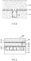
- FIGS. 1 to 4 each drawing is a schematic diagram wherein the dimensional ratio is not always exact, and the thickness of each layer is exaggerated with respect to the size of the substrate.
- a manufacturing method for a group III nitride semiconductor substrate 100 includes a process of forming an AlN layer 12 as a first group III nitride semiconductor layer on an Si substrate 10 as a substrate ( FIG. 1A ); a process of forming a GaN layer 14 as a second group III nitride semiconductor layer on the AlN layer 12 ( FIG. 1B , a first step); a process of forming an SiNx layer 18 as a protective layer on the GaN layer 14 ( FIG.
- FIG. 1C a second step
- FIG. 1D a third step
- FIG. 1E a fourth step
- the material of the substrate is not particularly limited and can be a sapphire substrate, a GaN substrate, Ga 2 O 3 substrate, and the like, in addition to the Si substrate used in the present embodiment.
- the Si substrate is advantageous in terms of productivity and cost performance because of easiness of obtaining a large area substrate and inexpensiveness.
- the plain orientation of the Si substrate surface is not particularly limited and can be (111), (100), (110), or the like.
- the thickness of the substrate may be appropriately set in consideration of the warpage of each layer after epitaxial growth.
- the AlN layer 12 is formed on the Si substrate 10.
- the first group III nitride semiconductor layer need not necessarily be formed.
- the thickness of the first group III nitride semiconductor layer is not particularly limited; however, when the AlN layer is to be formed on the Si substrate, the thickness can be set to 20 nm to 300 nm. When the thickness is smaller than 20 nm, the surface of the Si substrate cannot be sufficiently covered, so that Si and Ga unfavorably react with each other when GaN is grown on the Si substrate.
- the first group III nitride semiconductor layer may include a combination of AlN and AlGaN, a combination of AlN and InGaN aside from AlN alone.
- the first group III nitride semiconductor layer may be GaN, AlGaN, or InGaN.
- the second group III nitride semiconductor layer is formed on the substrate, specifically, the first group III nitride semiconductor layer.
- the GaN layer 14 is formed on the AlN layer 12.
- the thickness of the second group III nitride semiconductor layer is not particularly limited and may be set to 100 nm to 2000 nm. When the thickness is too small, a hollow is not formed in the following regrowth. Further, the thickness need not be so large since it is sufficient to form the hollow, and when the thickness is too large, a crack is highly likely to occur.
- the second group III nitride semiconductor layer may be AlN, AlGaN, or InGaN aside from GaN.
- dislocations are generated in the AlN layer 12 due to lattice mismatch between the Si substrate 10 and the AlN layer 12, and some dislocations 16 extend into the GaN layer 14 and reach the surface thereof.
- Such dislocations are generated due to lattice mismatch not only between the materials used in the present embodiment, but also between a different type substrate (substrate made of a material different from the group III nitride semiconductor) and the group III nitride semiconductor.
- the following processes are performed in order to prevent the dislocations 16 from extending to the surface of the group III nitride semiconductor substrate 100 to be finally obtained.
- a protective layer is formed on the second group III nitride semiconductor layer.
- the SiNx layer 18 is formed as the protective layer on the GaN layer 14.
- a material that is not easily etched by H 2 or NH 3 in a gas-phase etching process to be described later is acceptable as the material of the protective layer; however, SiNx or AlN is preferable as a commonly-used material capable of being grown by a MOCVD method which is most often used for growth of the group III nitride semiconductor layer.
- MOCVD method is most often used for growth of the group III nitride semiconductor layer.
- the SiNx layer as the protective layer is formed on the entire surface of the GaN layer 14, the third group III nitride semiconductor layer to be described later cannot be grown on the protective layer or, if can be grown, it will become polycrystalline.
- the SiNx layer 18 is grown discretely on the GaN layer 14.
- the coverage of the GaN layer by the SiNx layer is preferably 50% or more and less than 100% and, particularly preferably 50% or more and 95% or less.
- the growth time of the SiNx layer is preferably 30 sec to 20 min, more preferably, 3 min to 10 min.
- the substrate temperature at formation of the SiNx layer 18 is preferably 600°C to 1200°C and, particularly preferably, 900°C to 1200°C.
- the furnace pressure is preferably 10 hPa to 1000 hPa.
- the thickness of the SiNx layer 18 is preferably set to 1 nm to 50 nm and, particularly preferably, to 1 nm to 10 mm. When the thickness is smaller than 1 nm, dislocation selectivity at etching is insufficient, and when the thickness exceeds 50 nm, many dislocations are generated in SiNx due to relaxation of SiNx.
- the AlN layer is not used as the second group III nitride semiconductor layer, and the third group III nitride semiconductor layer can be grown on the protective layer, so that the AlN layer is preferably formed on the entire surface of the GaN layer 14.
- the thickness of the AlN layer is preferably set to 1 nm to 50 nm and, particularly preferably, to 1 nm to 20 nm. When the thickness is smaller than 1 nm, dislocation selectivity at etching is insufficient, and when the thickness exceeds 50 nm, many dislocations are generated in AlN due to relaxation of AlN.
- the substrate temperature at formation of the AlN layer is preferably 600°C to 1200°C and, particularly preferably, 900°C to 1200°C.
- the furnace pressure is preferably 10 hPa to 500 hPa.
- gas-phase etching is performed for the protective later and second group III nitride semiconductor layer.
- the gas-phase etching is applied to the SiNx layer 18 and GaN layer 14.
- the present inventors have found that pits can be selectively formed on dislocation portions on the second group III nitride semiconductor layer by performing the gas-phase etching under specific conditions after forming the protective layer on the second group III nitride semiconductor layer as described above.
- the pits 20 can be selectively formed on the dislocations 16 on the GaN layer 14. The thus formed pits 20 can prevent the dislocations 16 extending into the GaN layer 14 from evolving to the GaN layer 22 above the GaN layer 14.
- the pits 20 are formed so as to have a large depth relative to the opening diameter thereof, so that it remains even after formation of the subsequent GaN layer 22. That is, by performing the gas-phase etching under specific conditions after formation of the protective layer on the second group III nitride semiconductor layer, an angle ⁇ formed by a line connecting the opening end of the pits 20 and center of the bottom part thereof and the bottom part of the pits 20 can be 62° or larger. When the angle ⁇ is smaller than 62°, GaN is layered in the pits 20 in a process of growing the GaN layer 22, and the pits are undesirably fully filled.
- the gas-phase etching is preferably performed in a gaseous mixture atmosphere including H 2 , NH 3 , and optionally N 2 .
- inert gas such as Ar may be introduced, or etching gas such as Cl-based gas may be used.
- etching gas such as Cl-based gas may be used.
- a typical mixture gas of H 2 , NH 3 , and N 2 used in the growth of the group III nitride semiconductor is preferably employed.
- N 2 /(H 2 + NH 3 ) flow rate ratio is set to 0 to 0.5 and NH 3 /H 2 flow rate ratio is set to 0 to 0.08 and, particularly preferably, N 2 /(H 2 + NH 3 ) flow rate ratio is set to 0 to 0.2 and NH 3 /H 2 flow rate ratio is set to 0.001 to 0.02.
- the etching time is preferably set to 5 sec to 10 min.
- the gas-phase etching is preferably performed in a gaseous mixture atmosphere obtained by intermittently supplying NH 3 to an atmosphere including H 2 and optionally N 2 .
- etching occurs significantly in a period (hereinafter, referred to as "NH 3 stop period") during which supply of NH 3 is stopped, while dislocation selectivity for the pit tends to be low, and the opening diameter of the pit is likely to increase.
- NH 3 supply period a period during which NH 3 is supplied, etching slowly progresses, while dislocation selectivity for the pit tends to be high, and the opening diameter of the pit is unlikely to increase.
- N 2 /(H 2 + NH 3 ) flow rate ratio is set to 0 to 2
- NH 3 /H 2 flow rate ratio when the NH 3 is supplied is set to 0.001 to 2
- the NH 3 stop period is set to 1 sec to 20 sec
- the NH 3 supply period is set to 1 sec to 40 sec
- the number of times of repetition of a set of both the periods is dry to 5 to 200 in order to satisfy both the pit dislocation selectivity and pit depth
- N 2 /(H 2 + NH 3 ) flow rate ratio is set to 0 to 0.5
- NH 3 /H 2 flow rate ratio when the NH 3 is supplied is set to 0 to 1
- the NH 3 stop period is set to 1 sec to 6 sec
- the NH 3 supply period is set to 1 sec to 15 sec
- the number of times of repetition of a set of both the periods is set to 10 to 40.
- the total gas flow rate is preferably made constant in both the NH 3 stop period and NH 3 supply period.
- the flow rate of the H 2 gas is preferably made smaller than that in the NH 3 stop period by the amount corresponding to the gas flow rate of NH 3 .
- the substrate temperature at the gas-phase etching is preferably 900°C to 1200°C and, more preferably, 1000°C to 1100°C.
- the substrate temperature is lower than 900°C, an etching effect becomes low to make the pit unlikely to be formed.
- the substrate temperature exceeds 1200°C the pit dislocation selectivity may become low.
- the furnace pressure at the gas-phase etching is preferably 10 hPa to 500 hPa. It is structurally difficult to set the furnace pressure to a value lower than 10 hPa. When the furnace pressure exceeds 500 hPa, GaN (1-101) is generated, so that the pit is likely to be filled at the growth of the third group III nitride semiconductor layer to make the dislocation likely to extend into the third group III nitride semiconductor layer.
- the furnace pressure at the gas-phase etching is particularly preferably set to 10 hPa to 200 hPa.
- the furnace pressure at the gas-phase etching is particularly preferably set to 10 hPa to 300 hPa.
- more pits are preferably connected.
- the dislocations are associated to each other in the pit to be eliminated, so that the dislocation density of the GaN layer 22 can be reduced.
- the bit formation time is too long and the repetition number is too large, all the pits are connected to eliminate selectivity.
- it is necessary to set the bit formation time and the repetition number so as not to allow connection of all the pits.
- the third group III nitride semiconductor layer is formed on the second group III nitride semiconductor layer and/or the remaining protective layer.
- the GaN layer 22 is formed on the GaN layer 14 and/or remaining protective layer 18.
- the pits 20 remain.
- the thickness of the third group III nitride semiconductor layer is not particularly limited and is preferably set to 50 nm to 5000 nm. When the thickness is smaller than 50 nm, the surface is not sufficiently flattened. When the thickness is equal to or more than 5000 nm, a crack may occur.
- the remaining pits serve as hollows not having an oxide or a nitride.
- the third group III nitride semiconductor layer may be AlN, AlGaN, or InGaN aside from GaN.
- This process is preferably performed first under conditions wherein horizontal growth is prioritized and thereafter under conditions wherein the growth rate is prioritized. Even when the dislocation extends to the third group III nitride semiconductor layer, it can be bent in the horizontal direction under the conditions wherein the horizontal growth is prioritized to make it possible to reduce threading dislocation to the surface. Further, a portion where the pit is formed can be flattened to reduce surface roughness. Thereafter, the growth rate is prioritized to make it possible to increase productivity.
- the furnace pressure is set to 50 hPa to 500 hPa, V/III ratio is set to 500 to 50000, substrate temperature is set to 900°C to 1500°C, and growth time is set to 10 min to 120 min.
- the furnace pressure is set to 300 hPa to 3000 hPa, V/III ratio is set to 100 to 5000, and substrate temperature is set to 900°C to 1100°C, and the growth is continued until a target thickness is reached.
- the process of forming the third group III nitride semiconductor layer is performed first under conditions wherein formation of a facet plane inclined by 30° or more with respect to the growth plane is prioritized and thereafter under conditions wherein the horizontal growth is prioritized.
- the furnace pressure is set to 50 hPa to 3000 hPa
- V/III ratio is set to 10 to 10000
- substrate temperature is set to 900°C to 1500°C
- growth time is set to 1 min to 120 min.
- the conditions wherein the horizontal growth is prioritized are as described above, that is, preferably, the furnace pressure is set to 50 hPa to 500 hPa, V/III ratio is set to 500 to 50000, substrate temperature is set to 900°C to 1500°C, and growth time is set to 10 min to 120 min.
- the growth is continued under the conditions wherein the growth rate is prioritized until a target thickness is reached. According to this method, the nucleus density of GaN becomes low, and thus the dislocation can be propagated laterally with respect to the growth plane.
- the GaN layer 22 As the third group III nitride semiconductor layer, minute droplets of Ga are formed, and then regrowth of the initial nucleus of GaN from the Ga droplets may be promoted.
- the nucleus density of GaN becomes low, and thus the dislocation can be propagated laterally with respect to the growth plane.
- a formation method for the Ga droplets includes a first method of setting the V/III ratio to a predetermined level at a low temperature and a second method of forming a GaN crystal (group III nitride) at a low V/III ratio and then removing N from the GaN crystal under an H 2 atmosphere.
- the substrate temperature is set to 700°C to 1200°C
- furnace pressure is set to 20 hPa to 3000 hPa
- V/III ratio is set to 0 to 10.
- the substrate temperature is set to 700°C to 1100°C
- furnace pressure is set to 100 hPa to 1000 hPa
- V/III ratio is set to 0 to 1.
- a first condition for forming the Ga droplets is divided into a condition for forming the GaN crystal and a condition for removing N from the GaN crystal.
- the condition for forming the GaN crystal the substrate temperature is set to 900°C to 1500°C, furnace pressure is set to 50 hPa to 3000 hPa, and V/III ratio is set to 10 to 50000.
- the substrate temperature is set to 1000°C to 1200°C, furnace pressure is set to 500 hPa to 2000 hPa, and V/III ratio is set to 100 to 1000.
- the substrate temperature is set to 700°C to 1200°C
- furnace pressure is set to 20 hPa to 3000 hPa
- N 2 /(H 2 + NH 3 ) flow rate ratio is set to 0 to 4
- NH 3 /H 2 flow rate ratio is set to 0 to 1.
- the substrate temperature is set to 800°C to 1100°C
- furnace pressure is set to 100 hPa to 1000 hPa
- N 2 / (H 2 + NH 3 ) flow rate ratio is set to 0.2 to 2
- NH 3 /H 2 flow rate ratio is set to 0 to 0.4.
- the substrate temperature is set to 900°C to 1500°C
- furnace pressure is set to 300 hPa to 3000 hPa
- V/III ratio is set to equal to or more than 500.
- the method for forming the GaN layer by the Ga droplets may be applied not only to a case where the GaN layer 22 as the third group III nitride semiconductor layer is formed, but also to a case where the GaN layer 14 as the second group III nitride semiconductor layer. According to this method, the nucleus density of the GaN layer 14 becomes low, and thus the dislocation can be propagated laterally with respect to the growth plane.
- the substrate temperature is set to 900°C to 1200°C
- furnace pressure is set to 10 hPa to 1000 hPa
- N 2 / (H 2 + NH 3 ) flow rate ratio is set to 0.1 to 50
- NH 3 /H 2 flow rate ratio is set to equal to or more than 1.
- the substrate temperature is set to 1000°C to 1150°C
- furnace pressure is set to 10 hPa to 500 hPa
- N 2 /(H 2 + NH 3 ) flow rate ratio is set to 0.5 to 5
- NH 3 /H 2 flow rate ratio is set to equal to or more than 3.
- An SiNx layer as an additional protective layer may be formed on the SiNx layer 18 as the protective layer after selectively forming the pit 20 by the gas-phase etching at the dislocation portions on the GaN layer 14 as the second group III nitride semiconductor layer and before forming the GaN layer 22 as the third group III nitride semiconductor layer.
- the substrate temperature is preferably set to 600°C to 1200°C and, particularly preferably, to 900°C to 1200°C.
- the furnace pressure is preferably set to 10 hPa to 1000 hPa.
- the thickness of the additional SiNx layer is preferably set to 1 nm to 10 nm.
- the group III nitride semiconductor substrate of the present embodiment it is possible to efficiently obtain the group III nitride semiconductor substrate 100 with a low surface dislocation density in a single furnace.
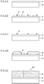
- FIG. 3 illustrates an example in which the second, third, and fourth steps are performed once again. That is, a protective layer 26 is formed on the GaN layer 22, pits 28 are selectively formed on dislocation portions 24 of the GaN layer 22 by the gas-phase etching, and a fourth group III nitride semiconductor layer is formed on the GaN layer 26 and/or remaining protective layer 26.
- the protective layer and conditions for the gas-phase etching have already been described, so descriptions thereof will be omitted. Further, description of the fourth group III nitride semiconductor layer is the same as that of the third group III nitride semiconductor layer and will therefore be omitted here.
- FIG. 4 illustrates an example in which the second and fourth steps are performed once again. That is, the protective layer 26 is formed on the GaN layer 22, and then the fourth group III nitride semiconductor layer is formed on the GaN layer 26 and/or remaining protective layer 26. In this case, as well, threading dislocation can be reduced in proportion to the suppression of extension of the dislocation 24.
- the group III nitride semiconductor substrates 100, 200, and 300 according to the first invention are each characterized by including the substrate 10, AlN layer 12 formed on the substrate 10 as the first group III nitride semiconductor layer, GaN layer 14 formed on the AlN layer 12 as the second group III nitride semiconductor layer, and GaN layer 22 formed on the GaN layer 14 as the third group III nitride semiconductor layer, wherein pits 20 are formed inside (surface layer part) the GaN layer 14.
- the dislocation 16 inside the GaN layer 14 is terminated by the pit 20, so that the dislocation density on the surface of the GaN layer 22 is reduced.
- the dislocation can be bent by designing the growth conditions of the GaN layer 22 as described above, so that the dislocation density on the surface of the GaN layer 22 is reduced.
- the density of the pits can be 1 ⁇ 10 8 cm 2 or higher, and the dislocation density on the surface of the GaN layer 22 as the third group III nitride semiconductor layer can be 1 ⁇ 10 8 cm 2 or lower.
- each drawing is a schematic diagram wherein the dimensional ratio is not always exact, and the thickness of each layer is exaggerated with respect to the size of the substrate.
- a manufacturing method for a group III nitride semiconductor substrate 400 includes a process of forming an AlN layer 12 as a first group III nitride semiconductor layer on an Si substrate 10 as a substrate ( FIG. 5A ); a process of forming a plurality of initial nuclei 32 and 34 made of GaN as a second group III nitride semiconductor on the AlN layer 12 ( FIG. 5B , a first step), a process of eliminating the initial nuclei 34 by the gas-phase etching ( FIG. 5C , a second step), and a process of forming a GaN layer 36 as a third group III nitride semiconductor layer on the Si substrate 10 and remaining initial nuclei 32 ( FIGS. 5D and 5E , a third step).
- the first group III nitride semiconductor layer 12 is the same as that in the first invention and will be omitted here. Many dislocations are generated in the AlN layer 12 due to lattice mismatch between the Si substrate 10 and the AlN layer 12.
- the first invention of the present application is a technique aiming to prevent the dislocations from extending to the surface of the group III nitride semiconductor substrate 400 to be finally obtained.
- the second invention to be described below is a technique aiming to suppress new dislocations that can be generated in a process of growing another group III nitride semiconductor layer on the first group III nitride semiconductor layer 12 (dislocations caused due to association between the initial nuclei that will be described later).
- a plurality of nuclei made of the second group III nitride semiconductor is formed on the substrate or the first group III nitride semiconductor layer.
- a plurality of initial nuclei (GaN grown to an island shape) 32 and 34 as the second group III nitride semiconductor are formed on the AlN layer 12. That is, at the initial stage of growth of GaN, such an initial nucleus is formed and then grown to be the GaN layer. In the present embodiment, the growth of GaN is stopped at the stage of the initial nucleus. At this time, there is a variation in size among the initial nuclei of GaN where large-sized initial nuclei 32 and small-sized initial nuclei 34 coexist.
- the second group III nitride semiconductor may be AlN, AlGaN, or InGaN aside from GaN.
- the maximum height of the initial nuclei is preferably set to 1 nm to 200 nm.
- the maximum height is smaller than 1 nm, the variation in size among the initial nuclei is so small that effects of the second invention to be described later cannot be sufficiently obtained.
- the maximum height exceeds 200 nm, a layer is undesirably formed.
- some initial nuclei have a diameter of 50 nm or larger, and some have a diameter of 5 nm or smaller.
- the initial nuclei 34 are eliminated by the gas-phase etching.
- An important point in this gas-phase etching is that the small-sized initial nuclei 34 are eliminated, but the large-sized initial nuclei 32 are made to remain although the size thereof becomes small.
- the dislocation 16 is generated when the adjacent initial nuclei are associated with each other in the growing process thereof.
- the third group III nitride semiconductor layer 36 is formed without the gas-phase etching after the formation of the initial nuclei in FIG. 5B , many initial nuclei whose sizes are varied but relatively close to one another densely populated, so that, as illustrated in FIG. 6 , the dislocation 16 is generated when the initial nuclei are associated with each other.
- the third group III nitride semiconductor layer 36 is formed with the density of the initial nuclei reduced by the gas-phase etching.
- a new initial nucleus 38 is formed; however, the remaining initial nucleus 32 grows bigger, with the result that the difference in size between the remaining initial nucleus 32 and newly generated initial nucleus 38 becomes large.
- the remaining large-sized initial nucleus 32 grows as if it swallowed the newly-generated initial nucleus 38, whereby the dislocation is not generated.
- the third group III nitride semiconductor layer 36 with less dislocation can be formed in the end.
- the gas-phase etching is preferably performed in a gaseous mixture atmosphere including H 2 , NH 3 , and optionally N 2 .
- inert gas such as Ar may be introduced, or etching gas such as Cl-based gas may be used.
- etching gas such as Cl-based gas may be used.
- a typical mixture gas of H 2 , NH 3 , and N 2 used in the growth of the group III nitride semiconductor is preferably employed.
- N 2 /(H 2 + NH 3 ) flow rate ratio is set to 0 to 0.5 and NH 3 /H 2 flow rate ratio is set to 0.001 to 0.08.
- the etching time is preferably set to 5 sec to 10 min.
- the gas-phase etching is preferably performed in a gaseous mixture atmosphere obtained by intermittently supplying NH 3 to an atmosphere including H 2 and optionally N 2 .
- etching occurs significantly in a period (hereinafter, referred to as "NH 3 stop period") during which supply of NH 3 is stopped, while the nucleus selectivity tends to be low, and all the nuclei are likely to be eliminated.
- NH 3 supply period a period during which NH 3 is supplied, etching slowly progresses, while the nucleus selectivity tends to be high, and large nuclei are hardly eliminated.
- N 2 /(H 2 + NH 3 ) flow rate ratio is set to 0 to 2
- NH 3 /H 2 flow rate ratio when the NH 3 is supplied is set to 0.001 to 2
- the NH 3 stop period is set to 1 sec to 20 sec
- the NH 3 supply period is set to 1 sec to 15 sec
- the number of times of repetition of a set of both the periods is set to 5 to 200 in terms of the nucleus selectivity.
- the total gas flow rate is preferably made constant in both the NH 3 stop period and NH 3 supply period.
- the flow rate of the H 2 gas is preferably made smaller than that in the NH 3 stop period by the amount corresponding to the gas flow rate of NH 3 .
- the substrate temperature at the gas-phase etching is preferably 900°C to 1200°C and, more preferably, 1000°C to 1100°C.
- the substrate temperature is lower than 900°C, the nucleus selectivity becomes low to make the nucleus unlikely to be etched.
- the substrate temperature exceeds 1200°C, the nucleus selectivity may become low.
- the furnace pressure at the gas-phase etching is preferably 50 hPa to 1000 hPa. It is structurally difficult to set the furnace pressure to a value lower than 50 hPa. When the furnace pressure exceeds 1000 hPa, it is difficult to stop growth of the third group III nitride semiconductor layer 36 while maintaining a nucleus state thereof.
- the third group III nitride semiconductor layer is formed on the substrate and remaining initial nuclei of the plurality of initial nuclei.
- the GaN layer 36 is formed on the substrate 10, AlN layer 12, and the remaining initial nuclei 32.
- the thickness of the third group III nitride semiconductor layer is not particularly limited and is preferably set to 10 nm to 5000 nm.
- the third group III nitride semiconductor layer may be AlN, AlGaN, or InGaN aside from GaN.
- This process is preferably performed first under conditions wherein horizontal growth is prioritized and thereafter under conditions wherein the growth rate is prioritized. Even when the dislocation extends to the third group III nitride semiconductor layer, it can be bent in the horizontal direction under the conditions wherein the horizontal growth is prioritized to make it possible to reduce threading dislocation to the surface. Thereafter, the growth rate is prioritized to make it possible to increase productivity. Specific conditions are the same as those in the first invention, so descriptions thereof will be omitted.
- the process of forming the GaN layer 36 as the third group III nitride semiconductor layer is performed first under conditions wherein formation of a facet plane inclined by 30° or more with respect to the growth plane is prioritized and thereafter under conditions wherein the horizontal growth is prioritized.
- Specific conditions are the same as those in the first invention, so descriptions thereof will be omitted. According to this method, the nucleus density of GaN becomes low, and thus the dislocation can be propagated laterally with respect to the growth plane.
- the GaN layer 36 In the process of forming the GaN layer 36, droplets of Ga are formed, and then regrowth of the initial nucleus of GaN from the Ga droplets may be promoted. Specific conditions are the same as those in the first invention, so descriptions thereof will be omitted. When the Ga droplets are crystallized, the nucleus density of GaN becomes low, and thus the dislocation can be propagated laterally with respect to the growth plane.
- the process of forming the GaN layer 36 it is preferable to perform heat treatment for flattening the upper surface of the GaN layer 36.
- Specific conditions are the same as those in the first invention, so descriptions thereof will be omitted. By performing the heat treatment under such conditions, it is possible to flatten the surface of the GaN layer without increasing the film thickness.
- the group III nitride semiconductor substrate of the present embodiment it is possible to efficiently obtain the group III nitride semiconductor substrate 400 with a low surface dislocation density in a single furnace.
- a protective layer on the substrate 10 and a plurality of initial nuclei 32 and 34 after the first step ( FIG. 5B ) and before the second step ( FIG. 5C ) .
- gas-phase etching after the formation of the protective layer, it is possible to increase a probability that the small-sized initial nuclei 34 are eliminated to thereby further suppress extension of the dislocation.
- a material that is not easily etched by H 2 or NH 3 in the subsequent gas-phase etching process is acceptable as the material of the protective layer; however, SiNx or AlN is preferable as a commonly-used material capable of being grown by a MOCVD method which is most often used for the growth of the group III nitride semiconductor layer.
- the SiNx layer as the protective layer As a raw material gas used for growing the SiNx layer, tetramethylsilane Si(CH 3 ) 4 as an Si raw material and NH 3 (ammonia) as an N raw material can be used.
- the SiNx layer as the protective layer is formed on the entire surface of the AlN layer 12, the third group III nitride semiconductor layer 36 cannot be grown on the protective layer or, if can be grown, it will become polycrystalline.
- the SiNx layer is grown discretely on the AlN layer 12.
- the coverage of the AlN layer by the SiNx layer is preferably 50% or more and less than 100% and, particularly preferably 50% or more and 95% or less. When the coverage is less than 50%, an effect brought about by formation of the protective layer cannot be sufficiently obtained. From this viewpoint, the growth time of the SiNx layer is preferably 30 sec to 20 min, more preferably, 3 min to 10 min.
- the third group III nitride semiconductor layer can be grown on the AlN layer, so that AlN layer is preferably formed on the entire surface of the AlN layer 12.
- the thickness of the AlN layer is preferably set to 1 nm to 10 nm. When the thickness is equal to or smaller than 1 nm, nucleus etching selectivity is insufficient, and when the thickness exceeds 10 nm, AlN having a large thickness remains after elimination of minute nuclei, thus impairing subsequent re-film formation.
- the first step ( FIG. 5B ) of forming the initial nucleus and the second step ( FIG. 5C ) of performing the gas-phase etching may be alternately repeated more than once.
- the number of times of repetition of a set of first and second steps is preferably set to 5 to 200. Details of the first and second steps have been already described. According to this method, the dislocation density can be further reduced.
- the plurality of initial nuclei of GaN are formed on the GaN layer 36, then the gas-phase etching is performed to eliminate some of the plurality of initial nuclei, and then the GaN layer as the fourth group III nitride semiconductor layer is formed on the GaN layer 36 and remaining initial nuclei. This can suppress the dislocation from newly occurring in the fourth group III nitride semiconductor layer.
- the group III nitride semiconductor substrate 400 according to the second invention is characterized by including the substrate 10 and the group III nitride semiconductor layer 36 formed on the substrate 10, wherein the dislocation density on the surface of the group III nitride semiconductor layer 36 is 1 ⁇ 10 8 cm 2 or lower.
- the present invention is not limited to the above embodiments, and may be variously modified without departing from the spirit of the present invention. Accordingly, all such modifications are included in the present invention.
- the AlN layer 12 as the first group III nitride semiconductor layer is formed on the upper surface of the substrate 10; alternatively, a multilayer film obtained by alternately laminating the AlN layer and GaN layer may be provided between the substrate 10 and the AlN layer 12 for the purpose of suppressing warpage of the substrate 10. That is, the first group III nitride semiconductor layer may not be formed directly on the upper surface of the substrate.
- the type of the multilayer film is not particularly limited as long as the invention can be achieved.
- An Si substrate having a (111) surface was washed with HF and SC-1 and introduced into an MOCVD furnace.
- the inside of the furnace was heated up to bake the Si substrate at a temperature of 1150°C to remove the oxide film on the Si surface.
- TMA as an Al raw material and NH 3 as an N raw material were introduced to form an AlN layer having a thickness of 100 nm on the Si substrate.
- the supply of TMA was interrupted, and the furnace temperature was reduced to and stabilized at 1050°C.
- TMG as a Ga raw material and NH 3 as an N raw material were introduced to form a GaN layer having a thickness of 1 ⁇ m on the AlN layer.
- SiNx layer As a protective layer on the GaN layer with the substrate temperature set to 1050°C, furnace pressure to 500 hPa, and growth time to 3 min.
- the thickness of the SiNx layer was 1nm, and the coverage of the GaN layer by the SiNx layer was 80%.
- the gas-phase etching was performed with N 2 / (H 2 + NH 3 ) flow rate ratio set to 0, NH 3 /H 2 flow rate ratio to 0.02, substrate temperature to 1050°C, furnace pressure to 100 hPa, and etching time to 10 min.
- N 2 / (H 2 + NH 3 ) flow rate ratio set to 0, NH 3 /H 2 flow rate ratio to 0.02, substrate temperature to 1050°C, furnace pressure to 100 hPa, and etching time to 10 min.
- the GaN layer was re-grown with the furnace pressure set to 400 hPa, V/III ratio to 2000, substrate temperature to 1150°C, and growth time to 10 min. These conditions gave priority to the horizontal growth and, as a result, the surface where the pits were formed was flattened to some extent. Thereafter, the GaN was grown to a thickness of 1 ⁇ m with the furnace pressure set to 500 hPa, V/III ratio to 1000, and substrate temperature to 1100°C to obtain a group III nitride semiconductor substrate.
- a group III nitride semiconductor substrate was obtained in the same manner as in the Example 1-1 except that the conditions for the gas-phase etching were changed.
- the gas-phase etching was performed in a gaseous mixture atmosphere obtained by intermittently supplying NH 3 to an H 2 atmosphere.
- the N 2 /(H 2 + NH 3 ) flow rate ratio was set to 0, NH 3 /H 2 flow rate ratio when supplying NH 3 was to 0.1, NH 3 stop period was to 6 sec, NH 3 supply period was to 10 sec, and the number of times of repetition of a set of both the NH 3 supply period and NH 3 stop period was to 40.
- the set of both periods was repeated 40 times with the flow rate of H 2 set to 19.4 slm for 6 sec, and the flow rates of H 2 and NH 3 set to 17.6 slm and 1.8 slm, respectively, for subsequent 10 seconds.
- the substrate temperature was set to 1050°C, and furnace pressure was to 390 hPa.
- a group III nitride semiconductor substrate was obtained in the same manner as in the Example 1-2 except that the AlN layer was formed as the protective layer.
- the AlN layer was formed, by introducing TMA as an Al raw material and NH 3 as an N raw material, on the entire surface of the GaN layer with a thickness of 10 nm.
- a group III nitride semiconductor substrate as illustrated in FIG. 3 was obtained by performing formation of the SiNx layer, gas-phase etching, and formation of the GaN layer in the same conditions as described above after the procedure of Example 1-2.
- a group III nitride semiconductor substrate as illustrated in FIG. 4 was obtained by performing formation of the SiNx layer and formation of the GaN layer in the same conditions as described above after the procedure of Example 1-2.
- a group III nitride semiconductor substrate was obtained in the same manner as in the Example 1-1 except that the gas-phase etching for forming pits in the GaN layer, and another SiNx layer is formed as an additional protective layer on the SiNx layer as the protective layer.
- the formation conditions for the additional protective layer were the same as those for the protective layer, and the thickness of the additional SiNx layer was set to 1 nm.
- a group III nitride semiconductor substrate was obtained in the same manner as in the Example 1-1 except that the GaN layer was re-grown.
- the GaN layer was re-grown under a first condition wherein the V/III ratio was comparatively low and thereafter under a second condition wherein the V/III ratio was comparatively high.
- the furnace pressure was set to 500 hPa, V/III ratio was to 1000, substrate temperature was to 1150°C, and growth time was to 5 min to give priority to the formation of the facet plane of the GaN layer.
- the furnace pressure was set to 500 hPa, V/III ratio was to 4000, substrate temperature was to 1150°C, and growth time was to 5 min to give priority to the horizontal growth of the GaN layer.
- the GaN was grown to a thickness of 1 ⁇ m with the furnace pressure set to 500 hPa, V/III ratio to 1000, and substrate temperature to 1100°C to obtain the group III nitride semiconductor substrate.
- a group III nitride semiconductor substrate was obtained in the same manner as in the Example 1-1 except that conditions for re-growth of the GaN layer were changed.
- the GaN layer was re-grown under a first condition wherein Ga droplets were formed according to a first method wherein the V/III ratio was set to a predetermined level at a low temperature and thereafter under a second condition wherein the Ga droplets were crystallized.
- the first condition the furnace pressure was set to 500 hPa, V/III ratio was to 0.5, substrate temperature was to 900°C, and growth time was to 10 min so as to form the Ga droplets.
- the furnace pressure was set to 500 hPa, V/III ratio was to 1000, substrate temperature was to 1050°C, and growth time was to 10 min so as to crystallize the Ga droplets. Thereafter, the GaN was grown to a thickness of 1 ⁇ m with the furnace pressure set to 500 hPa, V/III ratio to 1000, and substrate temperature to 1100°C to obtain the group III nitride semiconductor substrate.
- a group III nitride semiconductor substrate was obtained in the same manner as in the Example 1-1 except that conditions for re-growth of the GaN layer were changed.
- the GaN layer was re-grown under a first condition wherein a Ga crystal was formed at a low V/III ratio, then under a second condition wherein N was removed from the GaN crystal to form Ga droplets, and thereafter under a third condition wherein the Ga droplets were crystallized.
- the furnace pressure was set to 500 hPa
- V/III ratio was to 1000
- substrate temperature was to 1150°C
- growth time was to 5 min so as to form the GaN crystal.
- the furnace pressure was set to 500 hPa, N 2 /(H 2 + NH 3 ) flow rate ratio was to 1, and NH 3 /H 2 flow rate ratio was to 0, substrate temperature was to 900°C, and treatment time was to 10 min so as to remove N from the GaN crystal to form the Ga droplets.
- the furnace pressure was set to 500 hPa, V/III ratio was to 1000, substrate temperature was to 1050°C, and growth time was to 10 min so as to crystallize the Ga droplets. Thereafter, the GaN was grown to a thickness of 1 ⁇ m with the furnace pressure set to 500 hPa, V/III ratio to 1000, and substrate temperature to 1100°C to obtain the group III nitride semiconductor substrate.
- a group III nitride semiconductor substrate was obtained by performing heat treatment for fattening the GaN layer after the procedure of the Example 1-1.
- the furnace pressure was set to 500 hPa
- N 2 / (H 2 + NH 3 ) flow rate ratio was to 1.6
- NH 3 /H 2 flow rate ratio was to 0
- substrate temperature was to 1150°C
- treatment time was to 10 min.
- An Si substrate having a (111) surface was washed with HF and SC-1 and introduced into an MOCVD furnace.
- the inside of the furnace was heated up to bake the Si substrate at a temperature of 1150°C to remove the oxide film from the Si surface.
- TMA as an Al raw material and NH 3 as an N raw material were introduced to form an AlN layer having a thickness of 100 nm on the Si substrate.
- TMA As a Ga raw material and NH 3 as an N raw material were introduced to form many initial nuclei of GaN on the AlN layer.
- the furnace pressure was set to 400 hPa, V/III ratio was to 1000, and NH 3 /H 2 flow rate ratio was to 0.8.
- the initial nuclei had a height of up to 50 nm and had a diameter in a range of 5nm or less to 50 nm.
- the GaN layer was re-grown with the furnace pressure set to 400 hPa, V/III ratio to 2000, substrate temperature to 1150°C, and growth time to 10 min. These conditions gave priority to the horizontal growth and, as a result, GaN was grown on the remaining initial nucleus as if it swallowed the newly-generated initial nucleus. Thereafter, the GaN was grown to a thickness of 1 ⁇ m with the furnace pressure set to 500 hPa, V/III ratio to 1000, and substrate temperature to 1100°C to obtain a group III nitride semiconductor substrate.
- a group III nitride semiconductor substrate was obtained in the same manner as in the Example 2-1 except that a protective layer was formed on the initial nucleus of GaN immediately before the gas-phase etching of the Example 2-1.
- Tetramethylsilane Si(CH 3 ) 4 as an Si raw material and NH 3 as an N raw material were introduced as the protective layer to form an SiNx layer with the growth time set to 6 min.
- the coverage of the AlN layer by the SiNx layer was 80%.
- a group III nitride semiconductor substrate was obtained in the same manner as in the Example 2-2 except that the conditions for the gas-phase etching were changed.
- the gas-phase etching was performed in a gaseous mixture atmosphere obtained by intermittently supplying NH 3 to an H 2 atmosphere.
- the N 2 /(H 2 + NH 3 ) flow rate ratio was set to 0, NH 3 /H 2 flow rate ratio when supplying NH 3 was to 0.1, NH 3 stop period was to 6 sec, NH 3 supply period was to 10 sec, and the number of times of repetition of a set of both the NH 3 supply period and NH 3 stop period was to 40.
- the set of both periods was repeated 40 times with the flow rate of H 2 set to 19.4 slm for 6 sec, and the flow rates of H 2 and NH 3 set to 17.6 slm and 1.8 slm, respectively, for subsequent 10 seconds.
- the substrate temperature was set to 1050°C, and furnace pressure was to 390 hPa.
- a group III nitride semiconductor substrate was obtained in the same manner as in the Example 2-3 except that the AlN layer was formed as the protective layer.
- the AlN layer was formed, by introducing TMA as an Al raw material and NH 3 as an N raw material, on the entire surface of the GaN layer with a thickness of 10 nm.
- the GaN layer was grown by 50 nm after the gas-phase etching of the Example 2-3 was performed, and then formation of the SiNx layer and gas-phase etching were performed once again under the same conditions. Thereafter, the GaN layer was formed to a thickness of 1 ⁇ m as in the Example 2-1 to obtain a group III nitride semiconductor substrate.
- a group III nitride semiconductor substrate was obtained in the same manner as in the Example 2-3 except that the initial nucleus formation process and gas-phase etching process were alternately repeated 40 times.
- the substrate temperature was set to 1050°C
- furnace pressure was to 500 hPa
- V/III ratio was to 300.
- the gas-phase etching was performed in a gaseous mixture atmosphere obtained by intermittently supplying NH 3 to an H 2 atmosphere.
- the substrate temperature was set to 1050°C, furnace pressure was to 500 hPa, N 2 /(H 2 + NH 3 ) flow rate ratio was to 0.35, NH 3 /H 2 flow rate ratio was to 0.04, NH 3 stop period was to 10 sec, NH 3 supply period was to 30 sec, and the number of times of repetition of a set of both the NH 3 supply period and NH 3 stop period was to 20.
- An Si substrate having a (111) surface was washed with HF and SC-1 and introduced into an MOCVD furnace.
- the inside of the furnace was heated up to bake the Si substrate at a temperature of 1150°C to remove the oxide film on the Si surface.
- TMA as an Al raw material and NH 3 as an N raw material were introduced to form an AlN layer having a thickness of 100 nm on the Si substrate.
- the supply of TMA was interrupted, and the furnace temperature was reduced to and stabilized at 1050°C.
- TMG as a Ga raw material and NH 3 as an N raw material were introduced to form a GaN layer having a thickness of 2 ⁇ m on the AlN layer.
- a group III nitride semiconductor substrate 500 as illustrated in FIG. 8 was obtained.
- An Si substrate having a (111) surface was washed with HF and SC-1 and introduced into an MOCVD furnace.
- the inside of the furnace was heated up to bake the Si substrate at a temperature of 1150°C to remove the oxide film from the Si surface.
- TMA as an Al raw material and NH 3 as an N raw material were introduced to form an AlN layer having a thickness of 100 nm on the Si substrate.
- the supply of TMA was interrupted, and the furnace temperature was reduced to and stabilized at 1050°C.
- TMG as a Ga raw material and NH 3 as an N raw material were introduced to form a GaN layer having a thickness of 1 ⁇ m on the AlN layer.
- tetramethylsilane Si(CH 3 ) 4 as an Si raw material and NH 3 as an N raw material were introduced to form an SiNx layer as a protective layer on the GaN layer with the growth time set to 3 min.
- TMG as a Ga raw material and NH 3 as an N raw material were introduced once again to form a GaN layer having a thickness of 1 ⁇ m on the AlN layer. In this manner, a group III nitride semiconductor substrate 500 as illustrated in FIG. 9 was obtained.
- a group III nitride semiconductor substrate with a low surface dislocation density can be efficiently obtained.
Landscapes
- Chemical & Material Sciences (AREA)
- Metallurgy (AREA)
- Engineering & Computer Science (AREA)
- Materials Engineering (AREA)
- Organic Chemistry (AREA)
- Chemical Kinetics & Catalysis (AREA)
- General Chemical & Material Sciences (AREA)
- Mechanical Engineering (AREA)
- Inorganic Chemistry (AREA)
- Crystallography & Structural Chemistry (AREA)
- Crystals, And After-Treatments Of Crystals (AREA)
- Chemical Vapour Deposition (AREA)
- Drying Of Semiconductors (AREA)
- Led Devices (AREA)
Priority Applications (1)
| Application Number | Priority Date | Filing Date | Title |
|---|---|---|---|
| EP25211782.5A EP4665121A3 (de) | 2015-11-12 | 2016-11-01 | Herstellungsverfahren für gruppe-iii-nitrid-halbleitersubstrat und gruppe-iii-nitrid-halbleitersubstrat |
Applications Claiming Priority (2)
| Application Number | Priority Date | Filing Date | Title |
|---|---|---|---|
| JP2015222503 | 2015-11-12 | ||
| PCT/JP2016/082485 WO2017082126A1 (ja) | 2015-11-12 | 2016-11-01 | Iii族窒化物半導体基板の製造方法及びiii族窒化物半導体基板 |
Related Child Applications (2)
| Application Number | Title | Priority Date | Filing Date |
|---|---|---|---|
| EP25211782.5A Division-Into EP4665121A3 (de) | 2015-11-12 | 2016-11-01 | Herstellungsverfahren für gruppe-iii-nitrid-halbleitersubstrat und gruppe-iii-nitrid-halbleitersubstrat |
| EP25211782.5A Division EP4665121A3 (de) | 2015-11-12 | 2016-11-01 | Herstellungsverfahren für gruppe-iii-nitrid-halbleitersubstrat und gruppe-iii-nitrid-halbleitersubstrat |
Publications (4)
| Publication Number | Publication Date |
|---|---|
| EP3376525A1 true EP3376525A1 (de) | 2018-09-19 |
| EP3376525A4 EP3376525A4 (de) | 2019-10-23 |
| EP3376525B1 EP3376525B1 (de) | 2025-12-31 |
| EP3376525C0 EP3376525C0 (de) | 2025-12-31 |
Family
ID=58695274
Family Applications (2)
| Application Number | Title | Priority Date | Filing Date |
|---|---|---|---|
| EP25211782.5A Pending EP4665121A3 (de) | 2015-11-12 | 2016-11-01 | Herstellungsverfahren für gruppe-iii-nitrid-halbleitersubstrat und gruppe-iii-nitrid-halbleitersubstrat |
| EP16864089.4A Active EP3376525B1 (de) | 2015-11-12 | 2016-11-01 | Verfahren zur herstellung eines gruppe-iii-nitrid-halbleitersubstrats |
Family Applications Before (1)
| Application Number | Title | Priority Date | Filing Date |
|---|---|---|---|
| EP25211782.5A Pending EP4665121A3 (de) | 2015-11-12 | 2016-11-01 | Herstellungsverfahren für gruppe-iii-nitrid-halbleitersubstrat und gruppe-iii-nitrid-halbleitersubstrat |
Country Status (7)
| Country | Link |
|---|---|
| US (1) | US10777704B2 (de) |
| EP (2) | EP4665121A3 (de) |
| JP (2) | JP6489232B2 (de) |
| KR (2) | KR102081223B1 (de) |
| CN (2) | CN108352307B (de) |
| TW (1) | TWI623062B (de) |
| WO (1) | WO2017082126A1 (de) |
Cited By (1)
| Publication number | Priority date | Publication date | Assignee | Title |
|---|---|---|---|---|
| EP3758046A1 (de) * | 2019-06-28 | 2020-12-30 | Nokia Solutions and Networks Oy | Verfahren zum kombinieren von siliciummaterial und iii-v-material und zugehörige vorrichtung |
Families Citing this family (13)
| Publication number | Priority date | Publication date | Assignee | Title |
|---|---|---|---|---|
| CN108538977B (zh) * | 2018-03-16 | 2019-07-16 | 太原理工大学 | 一种高质量GaN薄膜及其制备方法 |
| JP7133786B2 (ja) * | 2018-10-29 | 2022-09-09 | パナソニックIpマネジメント株式会社 | Iii族窒化物半導体およびその製造方法 |
| JP7074038B2 (ja) * | 2018-12-04 | 2022-05-24 | 日本電信電話株式会社 | 半導体層の形成方法 |
| JP7158272B2 (ja) * | 2018-12-25 | 2022-10-21 | エア・ウォーター株式会社 | 化合物半導体基板 |
| CN113169052B (zh) * | 2018-12-27 | 2023-12-22 | 住友电气工业株式会社 | 氮化物半导体器件的制造方法 |
| JP7391297B2 (ja) * | 2019-06-28 | 2023-12-05 | 株式会社Flosfia | エッチング処理方法およびエッチング処理装置 |
| WO2021192075A1 (ja) * | 2020-03-25 | 2021-09-30 | 日本電信電話株式会社 | 半導体層の形成方法 |
| CN111554785B (zh) * | 2020-03-27 | 2021-10-08 | 华灿光电(苏州)有限公司 | 一种发光二极管外延片及其制备方法 |
| CN113540295B (zh) * | 2021-06-23 | 2023-07-21 | 山西中科潞安紫外光电科技有限公司 | 一种氮化铝衬底模板的制作方法 |
| JP7718026B2 (ja) * | 2021-08-30 | 2025-08-05 | 住友電工デバイス・イノベーション株式会社 | 半導体装置の製造方法 |
| CN114203535B (zh) * | 2021-12-09 | 2023-01-31 | 北京镓纳光电科技有限公司 | 高质量氮化铝模板及其制备方法和应用 |
| EP4239658A1 (de) * | 2022-03-03 | 2023-09-06 | Siltronic AG | Verfahren zur herstellung eines substratwafers zum darauf erstellen von gruppe-iii-v-vorrichtungen und substratwafer zum darauf erstellen von gruppe-iii-v-vorrichtungen |
| KR102728908B1 (ko) * | 2023-02-15 | 2024-11-13 | 웨이브로드 주식회사 | 이중 시드층을 이용한 그룹3족 질화물 반도체 템플릿의 제조 방법 |
Family Cites Families (22)
| Publication number | Priority date | Publication date | Assignee | Title |
|---|---|---|---|---|
| US6240115B1 (en) * | 1998-08-27 | 2001-05-29 | Agilent Technologies, Inc. | Epitaxial facet formation for laser diodes based on III-V material systems |
| JP3555500B2 (ja) | 1999-05-21 | 2004-08-18 | 豊田合成株式会社 | Iii族窒化物半導体及びその製造方法 |
| US6596079B1 (en) * | 2000-03-13 | 2003-07-22 | Advanced Technology Materials, Inc. | III-V nitride substrate boule and method of making and using the same |
| US6447604B1 (en) * | 2000-03-13 | 2002-09-10 | Advanced Technology Materials, Inc. | Method for achieving improved epitaxy quality (surface texture and defect density) on free-standing (aluminum, indium, gallium) nitride ((al,in,ga)n) substrates for opto-electronic and electronic devices |
| JP3476754B2 (ja) | 2000-07-28 | 2003-12-10 | 士郎 酒井 | 窒化ガリウム系化合物半導体の製造方法 |
| JP3988018B2 (ja) * | 2001-01-18 | 2007-10-10 | ソニー株式会社 | 結晶膜、結晶基板および半導体装置 |
| JP3583375B2 (ja) * | 2001-03-02 | 2004-11-04 | 三菱電線工業株式会社 | GaN系半導体基材およびその製造方法 |
| JP4631214B2 (ja) * | 2001-06-05 | 2011-02-16 | ソニー株式会社 | 窒化物半導体膜の製造方法 |
| JP4420128B2 (ja) | 2003-12-26 | 2010-02-24 | 日立電線株式会社 | Iii−v族窒化物系半導体デバイス及びその製造方法 |
| US7045808B2 (en) * | 2003-12-26 | 2006-05-16 | Hitachi Cable, Ltd. | III-V nitride semiconductor substrate and its production lot, and III-V nitride semiconductor device and its production method |
| JP4424497B2 (ja) * | 2005-02-15 | 2010-03-03 | 日立電線株式会社 | 窒化物半導体結晶の製造方法 |
| JP2007008742A (ja) * | 2005-06-29 | 2007-01-18 | Sumitomo Electric Ind Ltd | Iii族窒化物膜を形成する方法および半導体装置 |
| JP2007184503A (ja) * | 2006-01-10 | 2007-07-19 | Mitsubishi Chemicals Corp | 半導体部材及びその製造方法 |
| JP2008024554A (ja) * | 2006-07-21 | 2008-02-07 | Toyota Motor Corp | 単結晶の製造方法 |
| JP4538476B2 (ja) * | 2007-08-27 | 2010-09-08 | 独立行政法人理化学研究所 | 半導体構造の形成方法 |
| US8329565B2 (en) | 2008-11-14 | 2012-12-11 | Soitec | Methods for improving the quality of structures comprising semiconductor materials |
| KR101629733B1 (ko) | 2008-11-14 | 2016-06-21 | 소이텍 | 반도체 물질들을 포함하는 구조체들의 품질을 개선하는 방법들 |
| CN102656711B (zh) * | 2009-09-07 | 2015-07-08 | 松下电器产业株式会社 | 氮化物半导体多层结构体及其制造方法、氮化物半导体发光元件 |
| JP5995302B2 (ja) * | 2011-07-05 | 2016-09-21 | パナソニック株式会社 | 窒化物半導体発光素子の製造方法 |
| CN103614769B (zh) | 2013-10-25 | 2016-03-16 | 中国电子科技集团公司第五十五研究所 | 一种基于原位刻蚀的氮化镓同质外延方法 |
| JP2015151300A (ja) * | 2014-02-14 | 2015-08-24 | 日本電気硝子株式会社 | 赤外線センサー用光学ガラス |
| JP6315665B2 (ja) * | 2014-02-19 | 2018-04-25 | 古河機械金属株式会社 | Iii族窒化物半導体層およびiii族窒化物半導体基板の製造方法 |
-
2016
- 2016-11-01 US US15/773,391 patent/US10777704B2/en active Active
- 2016-11-01 EP EP25211782.5A patent/EP4665121A3/de active Pending
- 2016-11-01 CN CN201680063653.1A patent/CN108352307B/zh active Active
- 2016-11-01 KR KR1020197032151A patent/KR102081223B1/ko active Active
- 2016-11-01 JP JP2017550277A patent/JP6489232B2/ja active Active
- 2016-11-01 WO PCT/JP2016/082485 patent/WO2017082126A1/ja not_active Ceased
- 2016-11-01 KR KR1020187011924A patent/KR102041283B1/ko active Active
- 2016-11-01 CN CN202210395027.XA patent/CN115020192A/zh active Pending
- 2016-11-01 EP EP16864089.4A patent/EP3376525B1/de active Active
- 2016-11-09 TW TW105136477A patent/TWI623062B/zh active
-
2019
- 2019-01-16 JP JP2019004943A patent/JP2019089704A/ja active Pending
Cited By (1)
| Publication number | Priority date | Publication date | Assignee | Title |
|---|---|---|---|---|
| EP3758046A1 (de) * | 2019-06-28 | 2020-12-30 | Nokia Solutions and Networks Oy | Verfahren zum kombinieren von siliciummaterial und iii-v-material und zugehörige vorrichtung |
Also Published As
| Publication number | Publication date |
|---|---|
| CN115020192A (zh) | 2022-09-06 |
| EP3376525A4 (de) | 2019-10-23 |
| EP3376525B1 (de) | 2025-12-31 |
| EP4665121A2 (de) | 2025-12-17 |
| US20180337306A1 (en) | 2018-11-22 |
| TWI623062B (zh) | 2018-05-01 |
| CN108352307A (zh) | 2018-07-31 |
| CN108352307B (zh) | 2022-07-05 |
| JPWO2017082126A1 (ja) | 2018-08-30 |
| KR20190124830A (ko) | 2019-11-05 |
| US10777704B2 (en) | 2020-09-15 |
| TW201724377A (zh) | 2017-07-01 |
| EP3376525C0 (de) | 2025-12-31 |
| KR102081223B1 (ko) | 2020-02-25 |
| KR102041283B1 (ko) | 2019-11-06 |
| KR20180061287A (ko) | 2018-06-07 |
| JP6489232B2 (ja) | 2019-03-27 |
| JP2019089704A (ja) | 2019-06-13 |
| EP4665121A3 (de) | 2025-12-31 |
| WO2017082126A1 (ja) | 2017-05-18 |
Similar Documents
| Publication | Publication Date | Title |
|---|---|---|
| EP3376525B1 (de) | Verfahren zur herstellung eines gruppe-iii-nitrid-halbleitersubstrats | |
| US6403451B1 (en) | Methods of fabricating gallium nitride semiconductor layers on substrates including non-gallium nitride posts | |
| JP3886341B2 (ja) | 窒化ガリウム結晶基板の製造方法及び窒化ガリウム結晶基板 | |
| JP4720125B2 (ja) | Iii−v族窒化物系半導体基板及びその製造方法並びにiii−v族窒化物系半導体 | |
| US8178427B2 (en) | Epitaxial methods for reducing surface dislocation density in semiconductor materials | |
| JP4581490B2 (ja) | Iii−v族窒化物系半導体自立基板の製造方法、及びiii−v族窒化物系半導体の製造方法 | |
| US20030207125A1 (en) | Base substrate for crystal growth and manufacturing method of substrate by using the same | |
| US8652918B2 (en) | Nitride semiconductor structure | |
| KR20140107797A (ko) | 질화물 기판 제조 방법 | |
| JP5233894B2 (ja) | 窒化物半導体自立基板の製造方法 | |
| JP3698061B2 (ja) | 窒化物半導体基板及びその成長方法 | |
| JP4233894B2 (ja) | 半導体単結晶の製造方法 | |
| JP2012020934A (ja) | 窒化物半導体基板の製造方法 | |
| KR100764427B1 (ko) | 질화물 단결정 후막 제조방법 | |
| WO2010112540A1 (en) | Epitaxial methods and structures for reducing surface dislocation density in semiconductor materials | |
| KR20160063796A (ko) | 휨 및 깨짐 현상을 최소화시키기 위한 질화갈륨 웨이퍼 제조 방법 | |
| KR20170011932A (ko) | 화학 기상 식각을 이용한 저결함 질화물 반도체 기판 자가 분리 방법 | |
| KR20120072910A (ko) | 반도체 박막 성장 방법 및 이에 의해 성장된 반도체의 박막 | |
| JP2009208989A (ja) | 化合物半導体基板およびその製造方法 |
Legal Events
| Date | Code | Title | Description |
|---|---|---|---|
| STAA | Information on the status of an ep patent application or granted ep patent |
Free format text: STATUS: THE INTERNATIONAL PUBLICATION HAS BEEN MADE |
|
| PUAI | Public reference made under article 153(3) epc to a published international application that has entered the european phase |
Free format text: ORIGINAL CODE: 0009012 |
|
| STAA | Information on the status of an ep patent application or granted ep patent |
Free format text: STATUS: REQUEST FOR EXAMINATION WAS MADE |
|
| 17P | Request for examination filed |
Effective date: 20180511 |
|
| AK | Designated contracting states |
Kind code of ref document: A1 Designated state(s): AL AT BE BG CH CY CZ DE DK EE ES FI FR GB GR HR HU IE IS IT LI LT LU LV MC MK MT NL NO PL PT RO RS SE SI SK SM TR |
|
| AX | Request for extension of the european patent |
Extension state: BA ME |
|
| DAV | Request for validation of the european patent (deleted) | ||
| DAX | Request for extension of the european patent (deleted) | ||
| RIC1 | Information provided on ipc code assigned before grant |
Ipc: H01L 21/20 20060101AFI20190614BHEP Ipc: H01L 33/32 20100101ALI20190614BHEP Ipc: C30B 29/38 20060101ALI20190614BHEP Ipc: H01L 21/302 20060101ALI20190614BHEP Ipc: H01L 33/12 20100101ALI20190614BHEP Ipc: H01L 21/205 20060101ALI20190614BHEP Ipc: C23C 16/34 20060101ALI20190614BHEP Ipc: H01L 33/22 20100101ALI20190614BHEP |
|
| REG | Reference to a national code |
Ref country code: DE Ref legal event code: R079 Free format text: PREVIOUS MAIN CLASS: H01L0021205000 Ipc: H01L0021200000 |
|
| A4 | Supplementary search report drawn up and despatched |
Effective date: 20190923 |
|
| RIC1 | Information provided on ipc code assigned before grant |
Ipc: H01L 33/32 20100101ALI20190917BHEP Ipc: H01L 33/22 20100101ALI20190917BHEP Ipc: H01L 21/20 20060101AFI20190917BHEP Ipc: C23C 16/34 20060101ALI20190917BHEP Ipc: H01L 21/205 20060101ALI20190917BHEP Ipc: H01L 21/302 20060101ALI20190917BHEP Ipc: H01L 33/12 20100101ALI20190917BHEP Ipc: C30B 29/38 20060101ALI20190917BHEP |
|
| STAA | Information on the status of an ep patent application or granted ep patent |
Free format text: STATUS: EXAMINATION IS IN PROGRESS |
|
| 17Q | First examination report despatched |
Effective date: 20201119 |
|
| GRAP | Despatch of communication of intention to grant a patent |
Free format text: ORIGINAL CODE: EPIDOSNIGR1 |
|
| STAA | Information on the status of an ep patent application or granted ep patent |
Free format text: STATUS: GRANT OF PATENT IS INTENDED |
|
| RIC1 | Information provided on ipc code assigned before grant |
Ipc: H10H 20/825 20250101ALI20250604BHEP Ipc: H10H 20/82 20250101ALI20250604BHEP Ipc: H10H 20/815 20250101ALI20250604BHEP Ipc: H01L 21/205 20060101ALI20250604BHEP Ipc: H01L 21/20 20060101AFI20250604BHEP |
|
| INTG | Intention to grant announced |
Effective date: 20250703 |
|
| GRAS | Grant fee paid |
Free format text: ORIGINAL CODE: EPIDOSNIGR3 |
|
| GRAA | (expected) grant |
Free format text: ORIGINAL CODE: 0009210 |
|
| STAA | Information on the status of an ep patent application or granted ep patent |
Free format text: STATUS: THE PATENT HAS BEEN GRANTED |
|
| AK | Designated contracting states |
Kind code of ref document: B1 Designated state(s): AL AT BE BG CH CY CZ DE DK EE ES FI FR GB GR HR HU IE IS IT LI LT LU LV MC MK MT NL NO PL PT RO RS SE SI SK SM TR |
|
| REG | Reference to a national code |
Ref country code: CH Ref legal event code: F10 Free format text: ST27 STATUS EVENT CODE: U-0-0-F10-F00 (AS PROVIDED BY THE NATIONAL OFFICE) Effective date: 20251231 Ref country code: GB Ref legal event code: FG4D |
|
| REG | Reference to a national code |
Ref country code: DE Ref legal event code: R096 Ref document number: 602016094456 Country of ref document: DE |
|
| REG | Reference to a national code |
Ref country code: IE Ref legal event code: FG4D |
|
| U01 | Request for unitary effect filed |
Effective date: 20260127 |
|
| U07 | Unitary effect registered |
Designated state(s): AT BE BG DE DK EE FI FR IT LT LU LV MT NL PT RO SE SI Effective date: 20260130 |