EP4239658A1 - Verfahren zur herstellung eines substratwafers zum darauf erstellen von gruppe-iii-v-vorrichtungen und substratwafer zum darauf erstellen von gruppe-iii-v-vorrichtungen - Google Patents
Verfahren zur herstellung eines substratwafers zum darauf erstellen von gruppe-iii-v-vorrichtungen und substratwafer zum darauf erstellen von gruppe-iii-v-vorrichtungen Download PDFInfo
- Publication number
- EP4239658A1 EP4239658A1 EP22159979.8A EP22159979A EP4239658A1 EP 4239658 A1 EP4239658 A1 EP 4239658A1 EP 22159979 A EP22159979 A EP 22159979A EP 4239658 A1 EP4239658 A1 EP 4239658A1
- Authority
- EP
- European Patent Office
- Prior art keywords
- region
- single crystal
- silicon single
- nitrogen
- crystal wafer
- Prior art date
- Legal status (The legal status is an assumption and is not a legal conclusion. Google has not performed a legal analysis and makes no representation as to the accuracy of the status listed.)
- Pending
Links
Images
Classifications
-
- H—ELECTRICITY
- H10—SEMICONDUCTOR DEVICES; ELECTRIC SOLID-STATE DEVICES NOT OTHERWISE PROVIDED FOR
- H10P—GENERIC PROCESSES OR APPARATUS FOR THE MANUFACTURE OR TREATMENT OF DEVICES COVERED BY CLASS H10
- H10P95/00—Generic processes or apparatus for manufacture or treatments not covered by the other groups of this subclass
- H10P95/40—Treatments of semiconductor bodies to modify their internal properties, e.g. to produce internal imperfections
- H10P95/402—Treatments of semiconductor bodies to modify their internal properties, e.g. to produce internal imperfections of silicon bodies
- H10P95/405—Treatments of semiconductor bodies to modify their internal properties, e.g. to produce internal imperfections of silicon bodies using cavities formed by hydrogen or noble gas ion implantation
-
- H—ELECTRICITY
- H10—SEMICONDUCTOR DEVICES; ELECTRIC SOLID-STATE DEVICES NOT OTHERWISE PROVIDED FOR
- H10P—GENERIC PROCESSES OR APPARATUS FOR THE MANUFACTURE OR TREATMENT OF DEVICES COVERED BY CLASS H10
- H10P14/00—Formation of materials, e.g. in the shape of layers or pillars
- H10P14/20—Formation of materials, e.g. in the shape of layers or pillars of semiconductor materials
- H10P14/29—Formation of materials, e.g. in the shape of layers or pillars of semiconductor materials characterised by the substrates
- H10P14/2901—Materials
- H10P14/2902—Materials being Group IVA materials
- H10P14/2905—Silicon, silicon germanium or germanium
-
- H—ELECTRICITY
- H10—SEMICONDUCTOR DEVICES; ELECTRIC SOLID-STATE DEVICES NOT OTHERWISE PROVIDED FOR
- H10P—GENERIC PROCESSES OR APPARATUS FOR THE MANUFACTURE OR TREATMENT OF DEVICES COVERED BY CLASS H10
- H10P14/00—Formation of materials, e.g. in the shape of layers or pillars
- H10P14/20—Formation of materials, e.g. in the shape of layers or pillars of semiconductor materials
- H10P14/29—Formation of materials, e.g. in the shape of layers or pillars of semiconductor materials characterised by the substrates
- H10P14/2926—Crystal orientations
-
- H—ELECTRICITY
- H10—SEMICONDUCTOR DEVICES; ELECTRIC SOLID-STATE DEVICES NOT OTHERWISE PROVIDED FOR
- H10P—GENERIC PROCESSES OR APPARATUS FOR THE MANUFACTURE OR TREATMENT OF DEVICES COVERED BY CLASS H10
- H10P14/00—Formation of materials, e.g. in the shape of layers or pillars
- H10P14/20—Formation of materials, e.g. in the shape of layers or pillars of semiconductor materials
- H10P14/32—Formation of materials, e.g. in the shape of layers or pillars of semiconductor materials characterised by intermediate layers between substrates and deposited layers
- H10P14/3202—Materials thereof
- H10P14/3214—Materials thereof being Group IIIA-VA semiconductors
- H10P14/3216—Nitrides
-
- H—ELECTRICITY
- H10—SEMICONDUCTOR DEVICES; ELECTRIC SOLID-STATE DEVICES NOT OTHERWISE PROVIDED FOR
- H10P—GENERIC PROCESSES OR APPARATUS FOR THE MANUFACTURE OR TREATMENT OF DEVICES COVERED BY CLASS H10
- H10P14/00—Formation of materials, e.g. in the shape of layers or pillars
- H10P14/20—Formation of materials, e.g. in the shape of layers or pillars of semiconductor materials
- H10P14/32—Formation of materials, e.g. in the shape of layers or pillars of semiconductor materials characterised by intermediate layers between substrates and deposited layers
- H10P14/3242—Structure
- H10P14/3244—Layer structure
- H10P14/3251—Layer structure consisting of three or more layers
-
- H—ELECTRICITY
- H10—SEMICONDUCTOR DEVICES; ELECTRIC SOLID-STATE DEVICES NOT OTHERWISE PROVIDED FOR
- H10P—GENERIC PROCESSES OR APPARATUS FOR THE MANUFACTURE OR TREATMENT OF DEVICES COVERED BY CLASS H10
- H10P14/00—Formation of materials, e.g. in the shape of layers or pillars
- H10P14/20—Formation of materials, e.g. in the shape of layers or pillars of semiconductor materials
- H10P14/34—Deposited materials, e.g. layers
- H10P14/3402—Deposited materials, e.g. layers characterised by the chemical composition
- H10P14/3414—Deposited materials, e.g. layers characterised by the chemical composition being group IIIA-VIA materials
- H10P14/3416—Nitrides
-
- H—ELECTRICITY
- H10—SEMICONDUCTOR DEVICES; ELECTRIC SOLID-STATE DEVICES NOT OTHERWISE PROVIDED FOR
- H10P—GENERIC PROCESSES OR APPARATUS FOR THE MANUFACTURE OR TREATMENT OF DEVICES COVERED BY CLASS H10
- H10P14/00—Formation of materials, e.g. in the shape of layers or pillars
- H10P14/20—Formation of materials, e.g. in the shape of layers or pillars of semiconductor materials
- H10P14/36—Formation of materials, e.g. in the shape of layers or pillars of semiconductor materials characterised by treatments done before the formation of the materials
-
- H—ELECTRICITY
- H10—SEMICONDUCTOR DEVICES; ELECTRIC SOLID-STATE DEVICES NOT OTHERWISE PROVIDED FOR
- H10P—GENERIC PROCESSES OR APPARATUS FOR THE MANUFACTURE OR TREATMENT OF DEVICES COVERED BY CLASS H10
- H10P14/00—Formation of materials, e.g. in the shape of layers or pillars
- H10P14/60—Formation of materials, e.g. in the shape of layers or pillars of insulating materials
- H10P14/63—Formation of materials, e.g. in the shape of layers or pillars of insulating materials characterised by the formation processes
- H10P14/6302—Non-deposition formation processes
- H10P14/6316—Formation by nitridation, e.g. nitridation of the substrate
-
- H—ELECTRICITY
- H10—SEMICONDUCTOR DEVICES; ELECTRIC SOLID-STATE DEVICES NOT OTHERWISE PROVIDED FOR
- H10P—GENERIC PROCESSES OR APPARATUS FOR THE MANUFACTURE OR TREATMENT OF DEVICES COVERED BY CLASS H10
- H10P30/00—Ion implantation into wafers, substrates or parts of devices
- H10P30/20—Ion implantation into wafers, substrates or parts of devices into semiconductor materials, e.g. for doping
- H10P30/202—Ion implantation into wafers, substrates or parts of devices into semiconductor materials, e.g. for doping characterised by the semiconductor materials
- H10P30/204—Ion implantation into wafers, substrates or parts of devices into semiconductor materials, e.g. for doping characterised by the semiconductor materials into Group IV semiconductors
-
- H—ELECTRICITY
- H10—SEMICONDUCTOR DEVICES; ELECTRIC SOLID-STATE DEVICES NOT OTHERWISE PROVIDED FOR
- H10P—GENERIC PROCESSES OR APPARATUS FOR THE MANUFACTURE OR TREATMENT OF DEVICES COVERED BY CLASS H10
- H10P30/00—Ion implantation into wafers, substrates or parts of devices
- H10P30/20—Ion implantation into wafers, substrates or parts of devices into semiconductor materials, e.g. for doping
- H10P30/208—Ion implantation into wafers, substrates or parts of devices into semiconductor materials, e.g. for doping of electrically inactive species
-
- H—ELECTRICITY
- H10—SEMICONDUCTOR DEVICES; ELECTRIC SOLID-STATE DEVICES NOT OTHERWISE PROVIDED FOR
- H10P—GENERIC PROCESSES OR APPARATUS FOR THE MANUFACTURE OR TREATMENT OF DEVICES COVERED BY CLASS H10
- H10P36/00—Gettering within semiconductor bodies
- H10P36/03—Gettering within semiconductor bodies within silicon bodies
Definitions
- the invention provides a method for manufacturing a substrate wafer for building group III-V devices thereon and a substrate wafer for building group III-V devices thereon.
- Group III-V devices like high-electron-mobility transistors (HEMTs) are known for their superior performance in high power applications and high frequency applications. A vast amount of patent and non-patent literature dealing with this topic is available.
- HEMTs high-electron-mobility transistors
- US 2016 0 240 646 A1 discloses the structure and the fabrication of a couple of HEMT devices that may be built over a substrate wafer.
- a gettering region may be provided in a semiconductor substrate wafer.
- WO 2015 123 534 A1 discloses the provision of a buried implantation layer in a buffer region of the group III-V device in order to suppress a leakage current in the direction normal to the substrate.
- the inventor of the present invention has found that the substrate wafer needs to be improved, in particular in order to prevent dangling bonds from raising defect state densities and charge densities disturbing the proper function of the group III-V device.
- the present invention is directed to a method for manufacturing a substrate wafer for building group III-V devices thereon, comprising
- Dangling bonds are saturated or neutralized by providing at least one nitrogen enriched region that forms a nitrogen enriched passivation layer.
- the nitrogen enriched passivation layer does not form a separate silicon nitride layer deposited on the silicon single crystal wafer and lacks negative side effects of a separate layer. Moreover, impurities are trapped with a gettering region provided below the top surface of the silicon single crystal wafer.
- the nitrogen enriched passivation layer may be formed by diffusing nitrogen or implanting nitrogen ions in a top region of the silicon single crystal wafer.
- the silicon single crystal wafer may be subjected to an annealing step in a nitrogen containing gas atmosphere in order to diffuse nitrogen into the top region of the silicon single crystal wafer.
- the annealing step may be performed as a flash lamp anneal.
- the nitrogen containing atmosphere may contain nitrogen or ammonia (NH 3 ) or a mixture thereof.
- the annealing temperature may be in a range of not less than 300 °C and not more than 1350 °C.
- nitrogen ions may be implanted into a region under the top surface of the silicon single crystal wafer and, optionally, subjected to a following thermal treatment.
- the temperature of the following thermal treatment may be in a range of not less 300 °C and not more than 1350 °C.
- a further alternative comprises introducing nitrogen radicals generated in a plasma to the surface of the silicon single crystal wafer.
- the concentration of nitrogen that is additionally present at the surface of the silicon single crystal wafer is preferably not less than 1.0 ⁇ 10 11 atoms/cm 2 , but less than the quantity to form a stoichiometric silicon nitride layer on the surface of the silicon single crystal wafer.
- the density of silicon atoms with dangling bonds on the surface is thereby reduced to preferably less than 1 ⁇ 10 11 atoms/cm 2 , more preferably less than 1 ⁇ 10 10 atoms/cm 2 and most preferably less than 1 ⁇ 10 9 atoms/cm 2 .
- the nitrogen enriched passivation layer may be formed by depositing an AIN (aluminium nitride) nucleation layer contacting the top surface of the silicon single crystal wafer, and temporarily adding additional nitrogen during the deposition.
- the nitrogen concentration in the AIN nucleation layer is higher in a top region and a bottom region of the AIN nucleation layer compared to a region between the top region and the bottom region.
- the partial pressure of the nitrogen containing precursor gas may be temporarily increased during the deposition of the AIN nucleation layer.
- the deposition of the AIN nucleation layer may be performed as MOCVD (metal organic chemical vapor deposition), molecular ion-beam epitaxy (MBE).
- trimethylaluminum and ammonia can be used for MOCVD.
- Hydrogen or nitrogen is a suitable carrier gas.
- the growth temperature of the AIN layer is preferably not less than 700 °C and not more than 1250 °C for MOCVD, and not less than 400 °C and not more than 900 °C for MBE.
- the AIN nucleation layer has a thickness which is preferably not less than 10 nm and preferably not more than 500 nm, more preferably not more than 200 nm.
- the nitrogen enriched passivation layer in the top region of the AIN nucleation layer is not thicker than 10 nm and most preferably not more than 5 nm.
- additional nitrogen precursor gas is applied during the deposition of a bottom region and a top region of the AIN nucleation layer.
- the partial pressure of a nitrogen containing precursor gas may be temporarily increased during the deposition of the AIN nucleation layer.
- the concentration of nitrogen that is present in the bottom and the top region of the AIN nucleation layer is at least 1% higher than the Al concentration and at most 50 % higher than the Al concentration in the region between the top and bottom regions.
- a gettering region is formed below a top surface of the silicon single crystal wafer.
- the gettering region may be formed before the nitrogen enriched passivation layer is formed.
- the gettering region may be formed by implanting hydrogen ions into the silicon single crystal wafer and annealing the silicon single crystal wafer to form a layer of buried voids.
- the gettering region may be formed after the formation of the nitrogen enriched passivation layer by implanting the hydrogen ions into the substrate wafer from its back side and annealing the substrate wafer.
- the gettering region may be formed as an end-of-range damage (EOR) when the nitrogen ions are implanted in the top region of the silicon single crystal wafer to form the nitrogen enriched passivation layer by implanting nitrogen ions into the silicon single crystal wafer.
- EOR end-of-range damage
- the invention is directed to a substrate wafer for building group III-V devices, comprising
- the nitrogen enriched passivation layer may be part of the AIN nucleation layer contacting the top surface of the silicon single crystal wafer or may form a top portion of the silicon single crystal wafer.
- a concentration of nitrogen in the AIN nucleation layer is higher in a top region and a bottom region of the AIN nucleation layer compared to a region between the top region and the bottom region of the AIN nucleation layer.
- the gettering region may consist of a layer of buried voids or of an end-of-range damage.
- the silicon single crystal wafer may be a wafer cut from a silicon single crystal that has been grown according to the CZ-method by pulling a seed crystal from a melt contained in a crucible or FZ-method.
- the silicon single crystal wafer has a diameter that is at least 150 mm, preferably at least 200 mm and most preferably 300 mm.
- the lattice orientation of the silicon single crystal wafer may be preferably (100) or (111) or (110).
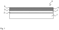
- Fig. 1 displays a sectional view of a substrate wafer according to the invention.
- the substrate wafer 6 displayed in Fig. 1 comprises a silicon single crystal wafer 1, a gettering region 2 and an AIN nucleation layer forming the nitrogen enriched passivation layer and consisting of a bottom region 3, a top region 5 and an intermediate region 4.
- the nitrogen concentration is higher in a top region 5 and the bottom region 3 compared to the nitrogen concentration in the intermediate region 4.
Landscapes
- Crystals, And After-Treatments Of Crystals (AREA)
- Recrystallisation Techniques (AREA)
Priority Applications (7)
| Application Number | Priority Date | Filing Date | Title |
|---|---|---|---|
| EP22159979.8A EP4239658A1 (de) | 2022-03-03 | 2022-03-03 | Verfahren zur herstellung eines substratwafers zum darauf erstellen von gruppe-iii-v-vorrichtungen und substratwafer zum darauf erstellen von gruppe-iii-v-vorrichtungen |
| CN202380024850.2A CN118830056A (zh) | 2022-03-03 | 2023-02-15 | 制造用于在其上构建iii-v族器件的衬底晶圆的方法和用于在其上构建iii-v族器件的衬底晶圆 |
| JP2024551633A JP7809826B2 (ja) | 2022-03-03 | 2023-02-15 | Iii-v族デバイスをその上に構築するための基板ウェハを製造するための方法、およびiii-v族デバイスをその上に構築するための基板ウェハ |
| KR1020247030379A KR20240140178A (ko) | 2022-03-03 | 2023-02-15 | Ⅲ-v족 디바이스들을 구축하기 위한 기판 웨이퍼를 제조하는 방법 및 ⅲ-v족 디바이스들을 구축하기 위한 기판 웨이퍼 |
| US18/841,402 US20250167005A1 (en) | 2022-03-03 | 2023-02-15 | Method for manufacturing a substrate wafer for building group iii-v devices thereon and a substrate wafer for building group iii-v devices thereon |
| PCT/EP2023/053694 WO2023165808A1 (en) | 2022-03-03 | 2023-02-15 | A method for manufacturing a substrate wafer for building group iii-v devices thereon and a substrate wafer for building group iii-v devices thereon |
| TW112107234A TWI885332B (zh) | 2022-03-03 | 2023-03-01 | 製造用於在其上構建iii-v族元件的基材晶圓的方法以及用於在其上構建iii-v族元件的基材晶圓 |
Applications Claiming Priority (1)
| Application Number | Priority Date | Filing Date | Title |
|---|---|---|---|
| EP22159979.8A EP4239658A1 (de) | 2022-03-03 | 2022-03-03 | Verfahren zur herstellung eines substratwafers zum darauf erstellen von gruppe-iii-v-vorrichtungen und substratwafer zum darauf erstellen von gruppe-iii-v-vorrichtungen |
Publications (1)
| Publication Number | Publication Date |
|---|---|
| EP4239658A1 true EP4239658A1 (de) | 2023-09-06 |
Family
ID=80628771
Family Applications (1)
| Application Number | Title | Priority Date | Filing Date |
|---|---|---|---|
| EP22159979.8A Pending EP4239658A1 (de) | 2022-03-03 | 2022-03-03 | Verfahren zur herstellung eines substratwafers zum darauf erstellen von gruppe-iii-v-vorrichtungen und substratwafer zum darauf erstellen von gruppe-iii-v-vorrichtungen |
Country Status (7)
| Country | Link |
|---|---|
| US (1) | US20250167005A1 (de) |
| EP (1) | EP4239658A1 (de) |
| JP (1) | JP7809826B2 (de) |
| KR (1) | KR20240140178A (de) |
| CN (1) | CN118830056A (de) |
| TW (1) | TWI885332B (de) |
| WO (1) | WO2023165808A1 (de) |
Citations (9)
| Publication number | Priority date | Publication date | Assignee | Title |
|---|---|---|---|---|
| KR100936869B1 (ko) * | 2007-12-10 | 2010-01-14 | 고려대학교 산학협력단 | 질화물 반도체소자 및 그 제조방법 |
| US20100046567A1 (en) * | 2008-08-22 | 2010-02-25 | The Regents Of The University Of California | Propagation of misfit dislocations from buffer/si interface into si |
| US20100065865A1 (en) * | 2008-09-18 | 2010-03-18 | Korea University Industrial & Academic Collaboration Foundation | Method of forming nitride semiconductor and electronic device comprising the same |
| US20140117502A1 (en) | 2012-10-25 | 2014-05-01 | Infineon Technologies Ag | Method for processing a semiconductor carrier, a semiconductor chip arrangement and a method for manufacturing a semiconductor device |
| WO2015123534A1 (en) | 2014-02-14 | 2015-08-20 | Dow Corning Corporation | Group iii-n substrate and transistor with implanted buffer layer |
| US20160240646A1 (en) | 2015-02-12 | 2016-08-18 | Taiwan Semiconductor Manufacturing Co., Ltd. | Low damage passivation layer for iii-v based devices |
| US20180174824A1 (en) * | 2016-12-20 | 2018-06-21 | Sumitomo Electric Device Innovations, Inc. | Process of forming epitaxial substrate and semiconductor device provided on the same |
| US20190013196A1 (en) * | 2017-07-10 | 2019-01-10 | M/A-Com Technology Solutions Holdings, Inc. | Parasitic channel mitigation via reaction with active species |
| EP3754721A1 (de) * | 2019-06-17 | 2020-12-23 | Infineon Technologies AG | Halbleiterbauelement und verfahren zur herstellung eines wafers |
Family Cites Families (8)
| Publication number | Priority date | Publication date | Assignee | Title |
|---|---|---|---|---|
| DE102006004870A1 (de) | 2006-02-02 | 2007-08-16 | Siltronic Ag | Halbleiterschichtstruktur und Verfahren zur Herstellung einer Halbleiterschichtstruktur |
| JP5668339B2 (ja) | 2010-06-30 | 2015-02-12 | 住友電気工業株式会社 | 半導体装置の製造方法 |
| DE102013218880A1 (de) * | 2012-11-20 | 2014-05-22 | Siltronic Ag | Verfahren zum Polieren einer Halbleiterscheibe, umfassend das gleichzeitige Polieren einer Vorderseite und einer Rückseite einer Substratscheibe |
| US10777704B2 (en) | 2015-11-12 | 2020-09-15 | Sumco Corporation | Manufacturing method for group III nitride semiconductor substrate and group III nitride semiconductor substrate |
| JP6759626B2 (ja) | 2016-02-25 | 2020-09-23 | 株式会社Sumco | エピタキシャルウェーハの製造方法およびエピタキシャルウェーハ |
| DE102016210203B3 (de) * | 2016-06-09 | 2017-08-31 | Siltronic Ag | Suszeptor zum Halten einer Halbleiterscheibe, Verfahren zum Abscheiden einer epitaktischen Schicht auf einer Vorderseite einer Halbleiterscheibe und Halbleiterscheibe mit epitaktischer Schicht |
| JP6868389B2 (ja) | 2016-12-27 | 2021-05-12 | 住友化学株式会社 | 半導体基板および電子デバイス |
| JP7044309B2 (ja) | 2020-08-03 | 2022-03-30 | 株式会社サイオクス | 窒化物半導体テンプレートおよび窒化物半導体デバイス |
-
2022
- 2022-03-03 EP EP22159979.8A patent/EP4239658A1/de active Pending
-
2023
- 2023-02-15 JP JP2024551633A patent/JP7809826B2/ja active Active
- 2023-02-15 CN CN202380024850.2A patent/CN118830056A/zh active Pending
- 2023-02-15 WO PCT/EP2023/053694 patent/WO2023165808A1/en not_active Ceased
- 2023-02-15 KR KR1020247030379A patent/KR20240140178A/ko active Pending
- 2023-02-15 US US18/841,402 patent/US20250167005A1/en active Pending
- 2023-03-01 TW TW112107234A patent/TWI885332B/zh active
Patent Citations (9)
| Publication number | Priority date | Publication date | Assignee | Title |
|---|---|---|---|---|
| KR100936869B1 (ko) * | 2007-12-10 | 2010-01-14 | 고려대학교 산학협력단 | 질화물 반도체소자 및 그 제조방법 |
| US20100046567A1 (en) * | 2008-08-22 | 2010-02-25 | The Regents Of The University Of California | Propagation of misfit dislocations from buffer/si interface into si |
| US20100065865A1 (en) * | 2008-09-18 | 2010-03-18 | Korea University Industrial & Academic Collaboration Foundation | Method of forming nitride semiconductor and electronic device comprising the same |
| US20140117502A1 (en) | 2012-10-25 | 2014-05-01 | Infineon Technologies Ag | Method for processing a semiconductor carrier, a semiconductor chip arrangement and a method for manufacturing a semiconductor device |
| WO2015123534A1 (en) | 2014-02-14 | 2015-08-20 | Dow Corning Corporation | Group iii-n substrate and transistor with implanted buffer layer |
| US20160240646A1 (en) | 2015-02-12 | 2016-08-18 | Taiwan Semiconductor Manufacturing Co., Ltd. | Low damage passivation layer for iii-v based devices |
| US20180174824A1 (en) * | 2016-12-20 | 2018-06-21 | Sumitomo Electric Device Innovations, Inc. | Process of forming epitaxial substrate and semiconductor device provided on the same |
| US20190013196A1 (en) * | 2017-07-10 | 2019-01-10 | M/A-Com Technology Solutions Holdings, Inc. | Parasitic channel mitigation via reaction with active species |
| EP3754721A1 (de) * | 2019-06-17 | 2020-12-23 | Infineon Technologies AG | Halbleiterbauelement und verfahren zur herstellung eines wafers |
Also Published As
| Publication number | Publication date |
|---|---|
| WO2023165808A1 (en) | 2023-09-07 |
| KR20240140178A (ko) | 2024-09-24 |
| TWI885332B (zh) | 2025-06-01 |
| TW202349462A (zh) | 2023-12-16 |
| CN118830056A (zh) | 2024-10-22 |
| JP7809826B2 (ja) | 2026-02-02 |
| US20250167005A1 (en) | 2025-05-22 |
| JP2025506905A (ja) | 2025-03-13 |
Similar Documents
| Publication | Publication Date | Title |
|---|---|---|
| US8476151B2 (en) | Method for manufacturing nitride semiconductor crystal layer | |
| KR101556054B1 (ko) | AlzGa1-zN 층을 갖는 반도체 웨이퍼 및 이를 제조하는 방법 | |
| US20050221591A1 (en) | Method of forming high-quality relaxed SiGe alloy layers on bulk Si substrates | |
| JP2004363592A (ja) | 十分に格子緩和された高品質SiGeオン・インシュレータ基板材料を製造する方法、基板材料、およびヘテロ構造 | |
| WO2008011688A2 (en) | GROWTH OF MONOCRYSTALLINE GeN ON A SUBSTRATE | |
| JP2018528614A (ja) | Iii族窒化物材料半導体構造における寄生チャネルの軽減 | |
| US11664223B2 (en) | Method for manufacturing a vertical power device including an III-nitride semiconductor structure | |
| US9147734B2 (en) | High quality GaN high-voltage HFETs on silicon | |
| CN115461502A (zh) | Iii-v族化合物晶体用基底基板及其制造方法 | |
| EP3731260A1 (de) | Verfahren zur herstellung eines gruppe-iii-nitrid-halbleitersubstrats | |
| JP2009094337A (ja) | 半導体素子の製造方法 | |
| US20120119332A1 (en) | Process for producing a semiconductor-on-sapphire article | |
| US20060246614A1 (en) | Method for manufacturing gallium nitride-based semiconductor device | |
| CN114220729B (zh) | 提高高电子迁移率晶体管外延片的质量的制备方法 | |
| EP4239658A1 (de) | Verfahren zur herstellung eines substratwafers zum darauf erstellen von gruppe-iii-v-vorrichtungen und substratwafer zum darauf erstellen von gruppe-iii-v-vorrichtungen | |
| KR100611108B1 (ko) | 박막 형성 방법 | |
| CN114023646A (zh) | 一种高阻值GaN基HEMT器件及其制备方法 | |
| US5674777A (en) | Method for forming silicon-boron binary compound layer as boron diffusion source in silicon electronic device | |
| US20060138540A1 (en) | Semiconductor wafer having a semiconductor layer and an electrically insulating layer beneath it, and process for producing it | |
| EP4400636A1 (de) | Verfahren zur herstellung eines nitridhalbleitersubstrats | |
| JP7673694B2 (ja) | Iii族窒化物半導体の製造方法 | |
| JP2010062219A (ja) | 炭化シリコンの製造方法 | |
| KR20240088776A (ko) | 헤테로에피택셜막의 제작방법 | |
| JP6714841B2 (ja) | 窒化物半導体装置の製造方法 | |
| JPH0425135A (ja) | 半導体基板 |
Legal Events
| Date | Code | Title | Description |
|---|---|---|---|
| PUAI | Public reference made under article 153(3) epc to a published international application that has entered the european phase |
Free format text: ORIGINAL CODE: 0009012 |
|
| STAA | Information on the status of an ep patent application or granted ep patent |
Free format text: STATUS: THE APPLICATION HAS BEEN PUBLISHED |
|
| AK | Designated contracting states |
Kind code of ref document: A1 Designated state(s): AL AT BE BG CH CY CZ DE DK EE ES FI FR GB GR HR HU IE IS IT LI LT LU LV MC MK MT NL NO PL PT RO RS SE SI SK SM TR |
|
| STAA | Information on the status of an ep patent application or granted ep patent |
Free format text: STATUS: REQUEST FOR EXAMINATION WAS MADE |
|
| 17P | Request for examination filed |
Effective date: 20240301 |
|
| RBV | Designated contracting states (corrected) |
Designated state(s): AL AT BE BG CH CY CZ DE DK EE ES FI FR GB GR HR HU IE IS IT LI LT LU LV MC MK MT NL NO PL PT RO RS SE SI SK SM TR |