EP3361479B1 - Anzeigegerät mit schieberegister und betriebsverfahren dafür - Google Patents
Anzeigegerät mit schieberegister und betriebsverfahren dafür Download PDFInfo
- Publication number
- EP3361479B1 EP3361479B1 EP16853096.2A EP16853096A EP3361479B1 EP 3361479 B1 EP3361479 B1 EP 3361479B1 EP 16853096 A EP16853096 A EP 16853096A EP 3361479 B1 EP3361479 B1 EP 3361479B1
- Authority
- EP
- European Patent Office
- Prior art keywords
- pull
- control signal
- node
- output
- shift register
- Prior art date
- Legal status (The legal status is an assumption and is not a legal conclusion. Google has not performed a legal analysis and makes no representation as to the accuracy of the status listed.)
- Active
Links
Images







Classifications
-
- G—PHYSICS
- G11—INFORMATION STORAGE
- G11C—STATIC STORES
- G11C19/00—Digital stores in which the information is moved stepwise, e.g. shift registers
- G11C19/18—Digital stores in which the information is moved stepwise, e.g. shift registers using capacitors as main elements of the stages
- G11C19/182—Digital stores in which the information is moved stepwise, e.g. shift registers using capacitors as main elements of the stages in combination with semiconductor elements, e.g. bipolar transistors, diodes
- G11C19/184—Digital stores in which the information is moved stepwise, e.g. shift registers using capacitors as main elements of the stages in combination with semiconductor elements, e.g. bipolar transistors, diodes with field-effect transistors, e.g. MOS-FET
- G11C19/186—Digital stores in which the information is moved stepwise, e.g. shift registers using capacitors as main elements of the stages in combination with semiconductor elements, e.g. bipolar transistors, diodes with field-effect transistors, e.g. MOS-FET using only one transistor per capacitor, e.g. bucket brigade shift register
-
- G—PHYSICS
- G11—INFORMATION STORAGE
- G11C—STATIC STORES
- G11C19/00—Digital stores in which the information is moved stepwise, e.g. shift registers
- G11C19/28—Digital stores in which the information is moved stepwise, e.g. shift registers using semiconductor elements
- G11C19/287—Organisation of a multiplicity of shift registers
-
- G—PHYSICS
- G09—EDUCATION; CRYPTOGRAPHY; DISPLAY; ADVERTISING; SEALS
- G09G—ARRANGEMENTS OR CIRCUITS FOR CONTROL OF INDICATING DEVICES USING STATIC MEANS TO PRESENT VARIABLE INFORMATION
- G09G3/00—Control arrangements or circuits, of interest only in connection with visual indicators other than cathode-ray tubes
- G09G3/20—Control arrangements or circuits, of interest only in connection with visual indicators other than cathode-ray tubes for presentation of an assembly of a number of characters, e.g. a page, by composing the assembly by combination of individual elements arranged in a matrix no fixed position being assigned to or needed to be assigned to the individual characters or partial characters
-
- G—PHYSICS
- G09—EDUCATION; CRYPTOGRAPHY; DISPLAY; ADVERTISING; SEALS
- G09G—ARRANGEMENTS OR CIRCUITS FOR CONTROL OF INDICATING DEVICES USING STATIC MEANS TO PRESENT VARIABLE INFORMATION
- G09G3/00—Control arrangements or circuits, of interest only in connection with visual indicators other than cathode-ray tubes
- G09G3/20—Control arrangements or circuits, of interest only in connection with visual indicators other than cathode-ray tubes for presentation of an assembly of a number of characters, e.g. a page, by composing the assembly by combination of individual elements arranged in a matrix no fixed position being assigned to or needed to be assigned to the individual characters or partial characters
- G09G3/2092—Details of a display terminals using a flat panel, the details relating to the control arrangement of the display terminal and to the interfaces thereto
- G09G3/2096—Details of the interface to the display terminal specific for a flat panel
-
- G—PHYSICS
- G09—EDUCATION; CRYPTOGRAPHY; DISPLAY; ADVERTISING; SEALS
- G09G—ARRANGEMENTS OR CIRCUITS FOR CONTROL OF INDICATING DEVICES USING STATIC MEANS TO PRESENT VARIABLE INFORMATION
- G09G2310/00—Command of the display device
- G09G2310/02—Addressing, scanning or driving the display screen or processing steps related thereto
- G09G2310/0264—Details of driving circuits
- G09G2310/0267—Details of drivers for scan electrodes, other than drivers for liquid crystal, plasma or OLED displays
-
- G—PHYSICS
- G09—EDUCATION; CRYPTOGRAPHY; DISPLAY; ADVERTISING; SEALS
- G09G—ARRANGEMENTS OR CIRCUITS FOR CONTROL OF INDICATING DEVICES USING STATIC MEANS TO PRESENT VARIABLE INFORMATION
- G09G2310/00—Command of the display device
- G09G2310/02—Addressing, scanning or driving the display screen or processing steps related thereto
- G09G2310/0264—Details of driving circuits
- G09G2310/0286—Details of a shift registers arranged for use in a driving circuit
-
- G—PHYSICS
- G09—EDUCATION; CRYPTOGRAPHY; DISPLAY; ADVERTISING; SEALS
- G09G—ARRANGEMENTS OR CIRCUITS FOR CONTROL OF INDICATING DEVICES USING STATIC MEANS TO PRESENT VARIABLE INFORMATION
- G09G2310/00—Command of the display device
- G09G2310/06—Details of flat display driving waveforms
- G09G2310/061—Details of flat display driving waveforms for resetting or blanking
-
- G—PHYSICS
- G09—EDUCATION; CRYPTOGRAPHY; DISPLAY; ADVERTISING; SEALS
- G09G—ARRANGEMENTS OR CIRCUITS FOR CONTROL OF INDICATING DEVICES USING STATIC MEANS TO PRESENT VARIABLE INFORMATION
- G09G2320/00—Control of display operating conditions
- G09G2320/02—Improving the quality of display appearance
- G09G2320/0252—Improving the response speed
Definitions
- the present invention relates to the field of display, more particularly to a display device comprising a shift register comprising a shift register unit and an operation method for the shift register unit of the display device.
- an output end of the shift register unit and a pull-up node are reset simultaneously by utilizing a special output reset transistor and a special node reset transistor.
- gates of an output reset transistor T4 and a node reset transistor T2 of the shift register unit are connected with a reset input end, and the output end and the pull-up node are reset respectively under control of a reset signal input by a reset input end.
- it requires enlarging an area of the output reset transistor T4, such that a turn-on voltage of the output reset transistor T4 is relatively small.
- enlarging the area of the reset transistor T4 is obviously not helpful to enhance resolution of a display device and narrow frame of the display device.
- US 2012/169703 A1 discloses a shift register circuit including a plurality of shift register stages for providing respective gate signals.
- Each shift register stage includes a driving unit, an input unit, a driving adjustment unit and a pull-down unit.
- the driving unit is for outputting a gate signal according to a system clock and a driving control voltage.
- the input unit is for outputting the driving control voltage according to an input control signal and a first input signal.
- the driving adjustment unit is for adjusting the driving control voltage according to a second input signal and a third input signal.
- the pull-down unit is for pulling down the gate signal and the driving control voltage according to a fourth input signal.
- US 2014/105351 A discloses a shift register including a plurality of shift register circuits, where each shift register circuit of the shift register includes a driving unit, a boost unit, a pull up unit, and a key pull down unit.
- the driving unit is for providing a gate signal, a first boost control signal, and a first transmission control signal according a first driving signal and a high frequency clock signal.
- the boost unit is for boosting the voltage of the first driving signal according to a first boost signal.
- the pull up unit is for providing a second driving signal according to the first transmission control signal and the gate signal, and for providing a second boost signal according to the first boost control signal and a second boost control signal.
- the key pull down unit is for pulling down the first driving signal according to a second transmission control signal.
- TW 201 514 959 A discloses a gate driving circuit.
- Each stage shift register of a gate driving circuit includes: a pull-up unit for pulling up a first transmission signal of an output line and a first gate signal of a gate line according to a driving voltage and a high-frequency clock signal; an energy-store unit for providing the driving voltage; a first driving unit for charging an energy-store unit of a subsequent stage shift register according to the first transmission signal and the first gate signal; a second driving unit for providing a pull-down control signal to the subsequent stage shift register according to the first transmission signal; a first pull-down unit for pulling down the driving voltage according to a first control signal; and a first control unit for generating the first control signal according to a first low-frequency clock signal and a pull-down control provided from a previous stage shift register.
- TW 201 532 058A discloses a shift register circuit having a plurality of shift registers. Each of the shift registers has at least four input terminals, a pull-up circuit, a first switch, a first pull-down circuit and a second pull-down circuit. A control terminal of the first switch is coupled to a node.
- the pull-up circuit pulls up a voltage level of the node.
- the first pull-down circuit pulls down a voltage level of an output terminal of the shift register.
- the second pull-down circuit pulls down the voltage level of the node.
- the four input terminals receive different clock signals, such that glitches on the node resulted from coupling effects of parasitic capacitor of the first switch is restrained, and positive bias stress (PBS) of two transistors of the first pull-down circuit and the second pull-down circuit is avoided.
- PBS positive bias stress
- CN 1 993 726 A discloses a shift register circuit.
- Each stage of a shift register circuit has a first input connected to the output of the preceding stage, a drive transistor for coupling a first clocked power line voltage to the output of the stage, a compensation capacitor for compensating for the effects of a parasitic capacitance of the drive transistor, a first bootstrap capacitor connected between the gate of the drive transistor and the output of the stage; and an input transistor for charging the first bootstrap capacitor and controlled by the first input.
- Each stage has an input section coupled to the output of the stage two stages before the stage having a second bootstrap capacitor connected between the gate of the input transistor and the first input.
- CN 104 464 645 A discloses a shifting register and a display device.
- the shifting register comprises a plurality of stages of shifting register units, and each shifting register unit comprises a first output control module, a second output control module, a graded output module and a pull-up node level maintaining capacitor, wherein the graded output module is connected with pull-up nodes, pull-down nodes, a carry signal output end and a driving signal output end and used for outputting carry signals and driving signals in a graded mode so that the driver signals can maintain a high level in the valuation stage and maintain a low level in the reset stage, the pre-charging stage and the non-work stage, the pull-up node level maintaining capacitor is connected between the first low level output end and the source of a first thin film transistor of the first output control module and used for maintaining the level of the pull-up nodes being a high level through the first output control module in the valuation state so that the driving signals can maintain the high level.
- CN 104 616 617 A discloses a shifting register and a drive method thereof as well as a grid drive circuit and a display device.
- the shifting register comprises a first input module, a second input module, an output module, an output pull-down module and a reset module which are all connected with a first node, wherein the first input module is for pulling up a potential at the first node under the action of a signal received from an input end; the output module is for pulling up a potential at an output end under the action of the potential at the first node; the reset module is for pulling down the potential at the first node under the action of a signal received from a reset end; the output pull-down module is for pulling down the potential at the output end under the action of a first clock signal; the second input module is for conducting the input end and the first node within working time of the first input module and the output pull-down module under the action of the first clock signal.
- US 2013/028370 A1 discloses a shift register formed by connecting unit circuits in multi-stage.
- One electrode of a capacitor Cap2 in the unit circuit is connected to the gate terminal (node N1) of a transistor T2, and the other connected to a node N2.
- a compensation circuit composed of transistors T3 to T5 provides a clock signal CKB to the node N2 when the node N1 potential is at low level, and applies a low-level potential to the node N2 when the node N1 potential is at high level. Accordingly, even when the gate potential of the transistor T2 changes with a change in a clock signal CK, a signal that cancels out the change is provided through the capacitor Cap2, stabilizing the gate potential of the transistor T2. Thus, a change in the control terminal potential of an output transistor associated with a change in a clock signal is prevented.
- CN 104 766 575A discloses a GOA circuit and a liquid crystal display.
- the GOA circuit comprises multiple GOA units, and each GOA unit performs charging on an Nth-stage horizontal scanning line G (N) and an N+1th-stage horizontal scanning line G (N+1) of a display area sequentially; each GOA unit comprises an N-stage pull-up control circuit, an N+1-stage pull-up control circuit, an N-stage pull-up circuit, an N+1-stage pull-up circuit, an N-stage pull-down circuit, an N+1-stage pull-down circuit and a pull-down holding circuit; after being charged at the Nth-stage horizontal scanning line G (N), each pull-down holding circuit holds the potential of an Nth-stage grid signal point Q (N) and the Nth-stage horizontal scanning line G (N) to be the low potential, and after being charged at the N+1th-stage horizontal scanning line G (N), each pull-down holding circuit holds the potential of an N+1th-stage grid signal point Q (N+1) and the N+1
- US 2011/058640 A1 discloses a shift register unit and a gate drive device for a liquid crystal display.
- the shift register unit on the basis of a structure of 12 transistors and 1 capacitor in the prior art, enables both the drain of the seventh thin film transistor and the gate and the drain of the ninth thin film transistor being connected to the second clock signal input terminal, such that a leakage current would not be generated among the seventh thin film transistor, the eighth thin film transistor, the ninth thin film transistor and the tenth thin film transistor when a high level signal is outputted from the shift register unit, thus power consumption of the shift register unit may be reduced.
- a shift register unit which is capable of not only reducing the area of the shift register unit but also reducing the reset time of the output end of the shift register unit.
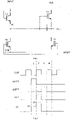
- Fig. 1 shows a schematic diagram of a structure of a shift register in the prior art.
- the shift register unit comprises an input transistor T1, an output transistor T3, a node reset transistor T2, an output reset transistor T4 and a capacitor C.
- a gate and a drain of the input transistor T1 are connected with an input end INPUT, a source of the input transistor T1 is connected with a pull-up node PU, a gate of the output transistor T3 is connected with a pull-up transistor, a drain of the output transistor T3 is connected with a clock signal end, a source of the output transistor T3 is connected with an output end OUT, gates of the output reset transistor T4 and the node reset transistor T2 are connected with the reset end RESET, sources of the output reset transistor T4 and the node reset transistor T2 are connected with a low power supply voltage end VSS, a drain of the output reset transistor T4 is connected with the output end OUT, and a drain of the node reset transistor T2 is connected with the pull-up node PU, a first end of the capacitor C is connected with the pull-up node PU, and another end of the capacitor C is connected with the output end OUT.
- Fig. 2 shows a timing diagram of the shift register unit as shown in Fig. 1 .
- the input end INPUT is at a high level
- the input transistor T1 is turned on to transmit the high level of the input end INPUT to the pull-up node PU.
- the pull-up node PU is in a first voltage V1, such that the output transistor T3 is turned on, and since a clock signal at a clock signal end CLK is at a low level, the output end OUT outputs the low level; in a second phase 2, the input end INPUT is at the low level, the input transistor T1 is turned off, the reset end RESET is at the low level, the node reset transistor T2 and the output reset transistor T4 are turned off, the pull-up node PU continues to make the output transistor T3 turned on, the clock signal at the clock signal end CLK is at the high level, and the output end OUT outputs the high level, and due to the effect of voltage-coupling of the capacitor C, the pull-up node PU is raised from the first voltage V1 to a second voltage V2 at this time; in a third phase 3, the reset end RESET is at the high level, the node reset transistor T2 and the output reset transistor T4 are turned on, and the pull-up node PU and the output end end
- the node reset transistor T2 and the output reset transistor T4 are utilized respectively to realize resetting of the pull-up node PU and the output end OUT, that is, resetting of the output end OUT is realized completely by the output reset transistor T4.
- the area of the output reset transistor T4 has to be enlarged, which is obviously not helpful to enhance the resolution of the display device and narrow the frame of the display device.
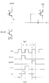
- Fig. 3 it shows a schematic diagram of a structure of another shift register unit in the prior art.
- the shift register unit comprises an input transistor T1, an output transistor T3, a node reset transistor T2, and a capacitor C.
- a gate of the node reset transistor T2 is connected with a node reset end RST_PU.
- connection manners of the input transistor T1, the output transistor T3, the node reset transistor T2 and the capacitor C are the same as those in Fig. 1 , and thus no further description is given herein.
- Fig. 4 shows a timing diagram of the shift register unit as shown in Fig. 3 .
- the operations of the shift register unit in the first phase 1 and the second phase 2 are the same as the operations as shown in Fig. 2 , and thus no further description is given herein;
- the clock signal end CLK is at the low level, the pull-up node PU makes the output transistor T3 maintain turned on, the output end OUT is pulled down to the low level of the clock signal end CLK, and at this time the pull-up node PU is in the first voltage VI;
- the node reset end RST_PU is at the high level, the node reset transistor T2 is turned on, and the pull-up node PU is pulled down to the low voltage of the low power supply voltage end VSS.
- the pull-up node PU maintains not reset and at the same time the output transistor T3 is utilized to pull down the output end OUT, and the pull-up node PU is controlled to be pulled down by the reset signal after the output end OUT is pulled down.
- the shift register unit as shown in Fig. 3 still cannot satisfy the requirements for further enhancing the resolution of the display device (for example, reaching UHD and a level higher than the UHD) and further narrowing the frame of the display device.
- Fig. 5 shows a schematic block diagram of a shift register unit for a display device according to an embodiment of the present invention.
- the shift register unit shown in Fig. 5 comprises: an input module 51, an output module 52, and a coupling module 53.
- a first end of the input module 51 is connected with an input end INPUT of the shift register unit and used to receive an input signal from the input end, and a second end thereof is connected with a pull-up node PU.
- the input module 51 is configured to transmit a received input signal to the pull-up node PU.
- a first end of the output module 52 is connected with the pull-up node PU, a second end thereof is connected with a first control signal end CON1, and a third end thereof is connected with an output end OUT of the shift register unit.
- the output module 52 is configured to output a first control signal of the first control signal end CON1 to the output end OUT when a pull-up signal at the pull-up node PU is in effective pull-up level.
- a first end of the coupling module 53 is connected with a second control signal end CON2, a second end thereof is connected with the pull-up node PU.
- the coupling module 53 is configured to control the pull-up signal at the pull-up node PU according to a second control signal of the second control signal end CON2 by way of voltage coupling.
- the coupling module 53 raises the pull-up signal at the pull-up node from a first pull-up voltage to a second pull-up voltage by way of voltage coupling according to the second control signal of the second control signal end CON2; and when the first control signal of the first control signal end CON1 jumps from the high level to the low level, a pull-up signal of a second pull-up voltage at the pull-up node makes the output module pull down the output end to the low level of the first control signal.
- the coupling module 53 is configured to utilize the second control signal of the second control signal end CON2 to perform voltage-coupling to control the pull-up signal at the pull-up node PU. Specifically, when the second control signal of the second control signal end CON2 jumps from a first level to a second level, the coupling module 53 make the pull-up signal at the pull-up node PU also have a voltage jump by way of voltage coupling, i.e., jumping from a first coupling voltage to a second coupling voltage.
- the coupling module 53 raises the pull-up signal at the pull-up node PU from a voltage VA to a voltage VB by way of voltage coupling.
- the coupling module 53 decreases the pull-up signal at the pull-up node PU from the voltage VC to the voltage CD by way of voltage coupling.
- the first control signal of the first control signal end CON1, the second control signal of the second control signal end CON2, and the output signal at the output end OUT are different from each other.
- a period of the first control signal is a first period, and the second control signal is prolonged 1/4 of the first period than the output signal.
- the coupling module raises the pull-up signal at the pull-up node from the first pull-up voltage to the second pull-up voltage by way of voltage coupling according to the second control signal of the second control signal end CON2, and then when the first control signal of the first control signal end CON1 jumps from the high level to the low level, the pull-up node PU being at the second pull-up voltage makes the output module pull down the output end to the low level of the first control signal.
- the output module outputs the first control signal to the output end when the pull-up signal at the pull-up node is in the first pull-up voltage and the second pull-up voltage.
- Fig. 6A shows an exemplary implementation of the coupling module 53 of the shift register unit according to an example not falling under the scope of the present invention defined in the claims.
- the coupling module 53 comprises a first capacitor C1, whose first end is connected with the second control signal end CON2 and second end is connected with the pull-up node PU.
- the coupling module 53 further comprises a third end, and the third end is connected with the third control signal end CON3. And the coupling module 53 is configured to: control the pull-up signal at the pull-up node PU by utilizing the third control signal of the third control signal end CON3 to perform voltage-coupling when the second control signal of the second control signal end CON2 is in effective control level. Specifically, when the second control signal of the second control signal end CON2 is in effective control level and when the third control signal of the third control signal end CON3 jumps from the first level to the second level, the coupling module 53 makes the pull-up signal at the pull-up node PU to have voltage jump by way of voltage-coupling, i.e., jumping from the first coupling voltage to the second coupling voltage.
- the coupling module 53 raises the pull-up signal at the pull-up node PU from the voltage VA to the voltage VB by way of voltage coupling.
- the coupling module 53 decreases the pull-up signal at the pull-up node PU from the voltage VC to the voltage VD by way of voltage coupling.
- the first control signal of the first control signal end CON1, the second control signal of the second control signal end CON2, the third control signal of the third control signal end CON3, and the output signal at the output end OUT are different from each other.
- the period of the first control signal is the first period
- the period of the third control signal is the second period
- the second period is 1/2 of the first period
- the second control signal is prolonged 1/4 of the first period than the output signal
- the duty ratio of the third control signal is smaller than or equal to 1/2
- the third control signal is in effective control level at both a jump-up edge and a jump-down edge of the first control signal.
- Fig. 6B shows an exemplary implementation of the coupling module 53 of the shift register unit according for a display device of the present invention.
- the coupling module 53 comprises a coupling transistor Tc and the first capacitor C1.
- a gate of the coupling transistor Tc is connected with the second control signal end CON2, and a first electrode thereof is connected with the third control signal end CON3.
- the first end of the first capacitor C1 is connected with a second electrode of the coupling transistor Tc, and the second end thereof is connected with the pull-up node PU.
- the gate of the coupling transistor Tc can be connected with the third control signal end CON3, and the first electrode thereof can be connected with the second control signal end CON2.
- Fig. 7A shows another schematic block diagram of a shift register unit for a display device of the present invention.
- the shift register unit shown in Fig. 7A further comprises: a reset module 54.
- a first end of the reset module 54 is connected with a fourth control signal end CON4, a second end thereof is connected with the pull-up node PU, and a third end thereof is connected with the low power supply voltage end VSS, and the reset module 54 is configured to pull down the pull-up signal at the pull-up node PU to the low power supply voltage of the low power supply voltage end VSS when a fourth control signal of the fourth control signal end CON4 is in effective control level.
- the fourth control signal of the fourth control signal end CON4 is prolonged 3/4 of the first period than the output signal at the output end.
- the reset module 54 further comprises a fourth end and a fifth end.
- the fourth end is connected with a fifth control signal end CON5
- the fifth end is connected with the output end OUT
- the reset module 54 is further configured to pull down the output signal at the output end OUT to the low power supply voltage of the low power supply voltage end VSS when a fifth control signal of the fifth control signal end CON5 is in effective control level.
- the fifth control signal of the fifth control signal end CON5 is prolonged 1/2 of the first period than the output signal at the output end OUT.
- Fig. 7B shows yet another schematic block diagram of the shift register unit for a display device of the present invention.
- the shift register unit shown in Fig. 7B further comprises a pull-down control module 55 and a pull-down module 56.
- a first end of the pull-down control module 55 is connected with a sixth control signal end CON6, a second end thereof is connected with the pull-up node PU, and a third end thereof is connected with the pull-down node PD.
- the pull-down control module 55 is configured: to generate, at the pull-down node PD, a pull-down signal which is in ineffective pull-down level when the pull-up signal at the pull-up node PU is in effective pull-up level, and to generate, at the pull-down node PD, a pull-down signal which is in effective pull-down level when the pull-up signal at the pull-up node PU is in ineffective pull-up level and a sixth control signal of the sixth control signal end CON6 is in effective control level.
- the sixth control signal of the sixth control signal end CON6 is prolonged 3/4 of the first period than the first control signal of the first control signal end CON1.
- a first end of the pull-down module 56 is connected with the pull-down node PD, a second end thereof is connected with the output end OUT, a third end thereof is connected with the pull-up node PU, and a fourth end thereof is connected with the low power supply voltage end VSS, and the pull-down module is configured to pull down the output end OUT and the pull-up node PU to the low power supply voltage of the low power supply voltage end VSS when the pull-down signal at the pull-down node PD is in effective pull-down level.
- the pull-down module 56 further comprises a fifth end, which is connected with a seventh control signal end CON7, and the pull-down module 56 is further configured to pull down the output end OUT to the low power supply voltage of the low power supply voltage end VSS when the seventh control signal of the seventh control signal end CON7 is in effective control level.
- the seventh control signal of the seventh control signal end CON7 is prolonged 1/2 of the first period than the first control signal of the first control signal end CON1.
- Fig. 8 shows an exemplary circuit implementation of the shift register unit according to an example not falling under the scope of the present invention defined in the claims.
- the shift register unit according to an example not falling under the scope of the present invention defined in the claims comprises the input module 51, the output module 52, the coupling module 53, the reset module 54, the pull-down control module 55 and the pull-up module 56.
- the input module 51 comprises an input transistor T1, whose gate and first electrode are connected with the input end INPUT and second electrode is connected with the pull-up node PU.
- the input transistor T1 transmits the input signal at the input end INPUT to the pull-up node PU.
- the output module 52 comprises an output transistor T3 and a second capacitor C2.
- a gate of the output transistor T3 and the first end of the second capacitor C2 are connected with the pull-up node PU, a first electrode of the output transistor T3 is connected with the first control signal end CON1, and a second electrode of the output transistor T3 and the second end of the second capacitor C2 are connected with the output end OUT.
- the output transistor T3 is turned on to output the first control signal of the first control signal end CON1 to the output end OUT.
- the coupling module 53 comprises a first capacitor C1, whose first end is connected with the second control signal CON2, and second end is connected with the pull-up node PU.
- first capacitor C1 raises the pull-up signal at the pull-up node PU from the voltage VA to the voltage VB by way of voltage coupling;
- second capacitor C2 decreases the pull-up signal at the pull-up node PU from the voltage VC to the voltage VD by way of voltage coupling.
- the reset module 54 comprises a node reset transistor T2, whose gate is connected with the fourth control signal end CON4, first electrode is connected with the pull-up node PU, and second electrode is connected with the low power supply voltage end VSS.
- the node reset transistor T2 When the fourth control signal of the fourth control signal end CON4 is in effective control level, the node reset transistor T2 is turned on to pull down the pull-up signal at the pull-up node PU to the low power supply voltage of the low power supply voltage end VSS.
- the pull-down control module 55 comprises a first pull-down control transistor T9, a second pull-down control transistor T10, a third pull-down control transistor T7 and a fourth pull-down control transistor T8.
- a gate and a first electrode of the first pull-down control transistor T9 are connected with the sixth control signal end CON6, and a second electrode thereof is connected with a pull-down control node PD_CN;
- a gate of the second pull-down control transistor T10 is connected with the pull-up node PU, a first electrode thereof is connected with a pull-down control node PD_CN, and a second electrode thereof is connected with the low power supply voltage end VSS;
- a gate of the third pull-down control transistor T7 is connected with the pull-down control node PD_CN, a first electrode thereof is connected with the sixth control signal end CON6, and second electrode thereof is connected with the pull-down node PD;
- a gate of the fourth pull-down control transistor T8 is connected with the pull-up node
- the pull-down module 56 comprises a node pull-down transistor T5 and an output pull-down transistor T6. Gates of the node pull-down transistor T5 and the output pull-down transistor T6 are connected with the pull-down node PD, second electrodes of the node pull-down transistor T5 and the output pull-down transistor T6 are connected with the low power supply voltage end VSS, a first electrode of the node pull-down transistor T5 is connected with the pull-up node PU, and a first electrode of the output pull-down transistor T6 is connected with the output end OUT.
- the node pull-down transistor T5 and the output pull-down transistor T6 are turned on to pull down the pull-up node PU and the output end OUT to the low power supply voltage of the low power supply voltage end VSS.
- the first control signal end CON1 is connected with the first clock signal end, the first control signal is the first clock signal, and the period of the first clock signal is the first period.
- the second control signal of the second control signal end CON1 is prolonged 1/4 of the first period than the output signal at the output end OUT.
- the fourth control signal of the fourth control signal end CON4 is prolonged 3/4 of the first period than the output signal at the output end.
- the sixth control signal of the sixth control signal end CON6 lags 3/4 of the first period than the first control signal of the first control signal end CON1.
- Fig. 9 shows an operation timing diagram of an exemplary circuit of the shift register unit according to an example not falling under the scope of the present invention defined in the claims.
- a first phase I input phase
- the input end INPUT is at a high level
- the input transistor T1 is turned on to transmit the high level of the input end INPUT to the pull-up node.
- the pull-up node is in a first high voltage V1, such that the output transistor T3 is turned on. Since the first control signal (i.e., first clock signal) of the first control signal end CON1 (i.e., first clock signal end CLK1) is at the low level, the output end OUT outputs the low level.
- the pull-up node PU is at the high level
- the second pull-down control transistor T10 and the fourth pull-down control transistor T8 are turned on, such that the pull-down node PD is at the low level, and correspondingly the node pull-down transistor T5 and the output pull-down transistor T6 are turned off.
- the fourth control signal of the fourth control signal end CON4 is at the low level, and the reset node transistor T2 is turned off.
- a second phase II (first output phase)
- the input end INPUT is at the low level
- the input transistor T1 is turned off
- the fourth control signal end CON4 is at the low level
- the node reset transistor T2 maintains turned off
- the pull-up node PU continues to make the output transistor T3 turned on
- the first control signal of the first control signal end CON1 is at the high level
- the output end OUT outputs the high level
- the pull-up node PU is raises from the first high voltage V1 to the second high voltage V2 at this time.
- a third phase III (second output phase)
- the input end INPUT is at the low level
- the input transistor T1 maintains turned off
- the fourth control signal CON4 is at the low level
- the node reset transistor T2 maintains turned off
- the second control signal of the second control signal end CON2 is at the high level
- the pull-up node PU is raised from the second high voltage V2 to the third high voltage V3 at this time.
- a fourth phase IV (first reset phase)
- the input end INPUT is at low level
- the input transistor T1 maintains turned off
- the fourth control signal end is at the low level
- the node reset transistor T2 maintains turned off
- the second control signal of the second control signal end CON2 is still at the high level
- the first control signal of the first control signal end CON1 jumps from the high level to the low level
- the pull-up node PU is stills at the high level
- the output transistor T3 is made to maintain turned off to pull down the output end OUT to the low level of the first control signal. Due to the effect of voltage-coupling of the second capacitor C2, the pull-up node PU decreases from the third high voltage V3 to the fourth high voltage V4 at this time.
- a fifth phase V (second reset phase)
- the second control signal of the second control signal end CON2 jumps from the high level to the low level, due to the effect of voltage-coupling of the first capacitor C1, the pull-up node PU starts to decrease from the fourth high voltage V4 (for example, decreasing to the first high voltage VI).
- the fourth control signal of the fourth control signal end CON4 is at the high level
- the node reset transistor T2 is turned on to pull down the pull-up node PU to the low voltage of the low power supply voltage end VSS.
- both the second pull-down control transistor T10 and the fourth pull-down control transistor T8 are turned off.
- both the first pull-down control transistor T9 and the third pull-down control transistor T7 are turned on, such that the pull-down node PD jumps from the low level to the high level, and correspondingly both the node pull-down transistor T5 and the output pull-down transistor T6 are turned on to pull down the pull-up node PU and the output end OUT to the low power supply voltage of the low power supply voltage end VSS.
- both the first pull-down control transistor T9 and the third pull-down control transistor T7 are turned off. Since the pull-up node PU is at the low level, both the second pull-down control transistor T10 and the fourth pull-down control transistor T8 maintain turned off, the pull-down node PD maintains at the high level, and correspondingly both the node pull-down transistor T5 and the output pull-down transistor T6 are turned on to pull down the pull-up node PU and the output end OUT to the low power supply voltage of the low power supply voltage end VSS.
- the fifth phase V and the sixth phase V1 are repeated until display of a next frame image starts, that is, the input end INPUT is again input an effective input signal.
- a voltage difference between the second high voltage V2 and the first high voltage V1 is ⁇ V1
- a voltage difference between the third high voltage V3 and the second high voltage V2 is ⁇ V2
- a voltage difference between the fourth high voltage V4 and the third high voltage V3 is ⁇ V3.
- the first high voltage, the second high voltage, the third high voltage, and the fourth high voltage are determined by a voltage value of the input signal at the input end INPUT, a voltage value of the first control signal of the first control signal end CON1, a voltage value of the second control signal of the second control signal end CON2, the first capacitor C1, the second capacitor C2 and a circuit parasitic capacitor.
- the pull-up signal at the pull-up node PU is in the third high voltage V3, and the third high voltage V3 is higher than the second high voltage V2 as shown in Figs.2 and 4 .
- Fig. 10 shows another exemplary circuit implementation of the shift register unit according toan example not falling under the scope of the present invention defined in the claims.
- the reset module 54 further comprises the output reset transistor T4, whose gate is connected with the fifth control signal end CON5, first electrode is connected with the output end OUT, and the second electrode is connected with the low power supply voltage end VSS.
- the fifth control signal of the fifth control signal end CON5 is prolonged 1/2 of the first period than the output signal at the output end OUT.
- the fifth control signal of the fifth control signal end CON5 is at the high level, and the output reset transistor T4 is turned on to pull down the output end OUT to the low power supply voltage of the low power supply voltage end VSS.
- Driving capacity of the output end OUT can be enhanced by adding the output reset transistor T4.
- the output end OUT can be pulled down to the low power supply voltage of the low power supply voltage end VSS more quickly by the cooperation of the output transistor T3 and the output reset transistor T4.
- Fig. 11 shows yet another exemplary circuit implementation of the shift register unit according to an example not falling under the scope of the present invention defined in the claims.
- the pull-down module 56 further comprises a clock pull-down transistor T11, whose gate is connected with the seventh control signal end CON7, first electrode is connected with the output end OUT, and second electrode is connected with the low power supply voltage end VSS.
- the seventh control signal of the seventh control signal end CON7 is prolonged 1/2 of the first period than the first clock signal.
- the seventh control signal of the seventh control signal end CON7 is at the high level, the clock pull-down transistor T11 is turned on to pull down the output end OUT to the low power supply voltage of the low power supply voltage end VSS.
- Driving capacity of the output end OUT can be enhanced by adding the clock pull-down transistor T11, and the output end OUT can be pulled down to the low power supply voltage of the low power supply voltage end VSS faster through the cooperation of the output transistor T3 and the clock pull-down transistor T11.
- Fig. 12 shows a schematic block diagram of the shift register unit according to an example not falling under the scope of the present invention defined in the claims.
- the shift register according to an example not falling under the scope of the present invention defined in the claims comprises a plurality of shift register units connected in cascades, each of which can be as shown in Fig. 8 .
- the shift register unit is connected with a start input signal end STV, a first clock signal end CLK1, a second clock signal end CLK2, a third clock signal end CLK1B and a fourth clock signal end CLK2B.
- Periods of a first clock signal at the first clock signal end CLK1, a second clock signal at the second clock signal end CLK2, a third clock signal at the third clock signal end and a fourth clock signal at the fourth clock signal end CLK2B are the first period
- the second clock signal is prolonged 1/4 of the first period than the first clock signal
- the third clock signal is prolonged 1/4 of the first period than the second clock signal
- the fourth clock signal is prolonged 1/4 of the first period than the third clock signal.
- Input ends INPUT of first and second stages of shift register units are connected with an initial input signal end STV to receive an initial input signal, an input end of a (2j+1)-th stage of shift register unit is connected with an output end of a (2j-1)-th stage of shift register unit, and an input end of a (2j+2)-th stage of shift register unit is connected with an output end of a (2j)-th stage of shift register unit, where j is a positive integer greater than or equal to 1.
- a first control signal end of a (4i+1)-th stage of shift register unit is connected with the first clock signal end CLK1, a second control signal end thereof is connected with an output end of a (4i+2)-th stage of shift register unit, a fourth control signal end thereof is connected with an output end of a (4i+4)-th stage of shift register unit, and a sixth control signal end thereof is connected with the fourth clock signal end CLK2B, where i is an integer greater than or equal to 0.
- a first control signal end of a (4i+2)-th stage of shift register unit is connected with the second clock signal end CLK2, a second control signal end thereof is connected with an output end of a (4i+3)-th stage of shift register unit, a fourth control signal thereof is connected with an output end of a (4i+5)-th stage of shift register unit, and a sixth control signal end thereof is connected with a first clock signal end CLK1.
- a first control signal end of a (4i+3)-th stage of shift register unit is connected with the third clock signal end CLK1B, a second control signal end thereof is connected with an output end of a (4i+4)-th stage of shift register unit, a fourth control signal end thereof is connected with an output end of a (4i+6)-th stage of shift register unit, and a sixth control signal thereof is connected with the second clock signal end CLK2.
- a first control signal end of a (4i+4)-th stage of shift register unit is connected with the fourth clock signal end CLK2B, a second control signal end thereof is connected with an output end of a (4i+5)-th stage of shift register unit, a fourth control signal end thereof is connected with an output end of a (4i+7)-th stage of shift register unit, and a sixth control signal end thereof is connected with the third clock signal end CLK1B.
- each shift register unit being the shift register unit as shown in Fig. 10 .
- a fifth control signal end of the (2j-1)-th stage of shift register unit is connected with an output end of the (2j+1)-th stage of shift register unit, and a fifth control signal end of the (2j)-th stage of shift register unit is connected with an output end of the (2j+2)-th stage of shift register unit, where j is an integer greater than or equal to 1.
- each shift register unit being the shift register unit as shown in Fig. 11
- a seventh control signal end of the (4i+1)-th stage of shift register unit is connected with the third clock signal end CLK1B
- a seventh control signal end of the (4i+2)-th stage of shift register unit is connected with the fourth clock signal end CLK2B
- a seventh control signal end of the (4i+3)-th stage of shift register unit is connected with the first clock signal end CLK1
- a seventh control signal end of the (4i+1)-th stage of shift register unit is connected with the second clock signal end CLK2, where i is an integer greater than or equal to 0.
- FIG. 9 it also shows an output signal GL1 of a first stage of shift register unit, an output signal GL2 of a second stage of shift register unit, an output signal GL3 of a third stage of shift register unit, and an output signal GL4 of a fourth stage of shift register unit.
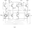
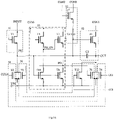
- Fig. 13 shows an exemplary circuit implementation of the shift register unit for a display device of the present invention.
- the shift register unit comprises an input module 51, an output module 52, a coupling module 53, a reset module 54, a pull-down control module 55 and a pull-down module 56.
- Circuit structure of the input module 51, the output module 52, the reset module 54, the pull-down control module 55 and the pull-down module 56 in Fig. 13 is the same as the circuit structure of the input module 51, the output module 52, the reset module 54, the pull-down control module 55 and the pull-down module 56 in Fig. 8 , and thus no further description is given herein.
- the coupling module 53 comprises a coupling transistor Tc and a first capacitor C1.
- a gate of the coupling transistor Tc is connected with the second control signal end CON2, a first electrode thereof is connected with the third control signal end CON3.
- a first end of the first capacitor C1 is connected with a second electrode of the coupling transistor Tc, and a second end thereof is connected with the pull-up node PU.
- the gate of the coupling transistor Tc can be connected with the third control signal end CON3, and the first electrode thereof can be connected with the second control signal end CON2.
- the first control signal end CON1 is connected with the first clock signal end CLK1, the first control signal is a first clock signal, and a period of the first clock signal is a first period.
- the second control signal of the second control signal end CON2 is prolonged 1/4 of the first period than the output signal at the output end OUT.
- the third control signal of the third control signal end CON3 is a pulse signal.
- a period of the pulse signal is a second period, which is 1/2 of the first period, a duty ratio of the pulse signal is smaller than or equal to 1/2, and the third control signal is in effective control level at both the jump-up edge and the jump-down edge of the first control signal.
- the fourth control signal of the fourth control signal end CON4 is prolonged 3/4 of the first period than the output signal at the output end.
- the sixth control signal of the sixth control signal end CON6 is prolonged 3/4 of the first period than the first control signal of the first control signal end CON1.
- Fig. 14 shows an operation timing diagram of an exemplary circuit of the shift register unit for a display device of the present invention.
- a first phase I (input phase)
- the second control signal of the second control signal end CON2 is at the low level, and the coupling transistor Tc is turned off. Remaining operations in the first phase I are the same as the operations in the first phase I as shown in Fig. 9 , and thus no further description is given herein.
- the pull-up node is in the first high voltage V1.
- a second phase II (first output phase)
- the second control signal of the second control signal end CON2 is still at the low level, and the coupling transistor Tc maintains turned off. Remaining operations in the second phase II are the same as the operations in the first phase I as shown in Fig. 9 , and thus no further description is given herein.
- the output end OUT outputs the high level, and due to the effect of voltage-coupling of the second capacitor C2, at this time the pull-up node PU is raised from the first high voltage V1 to the second high voltage V2.
- a third phase III (second output phase)
- the second control signal of the second control signal end CON2 is at the high level
- the coupling transistor Tc is turned on
- the third control signal end CON3 is at the low level
- the voltage of the pull-up node PU maintains in the second high voltage V2. Remaining operations in the third phase III are the same as the operations in the third phase III as shown in Fig. 9 , and thus no further description is given herein.
- a fourth phase IV (third output phase)
- the second control signal of the second control signal end CON2 is at the high level
- the coupling transistor Tc is turned on
- the third control signal end CON3 jumps from the low level to the high level
- the voltage of the pull-up nod PU is raised form the second high voltage V2 to the third high voltage V3.
- Remaining operations in the fourth phase IV are the same as the operations in the third phase III as shown in Fig. 9 , and thus no further description is given herein.
- a fifth phase V (first reset phase)
- the second control signal of the second control signal end CON2 is still at the high level
- the coupling transistor Tc maintains turned on
- the third control signal end CON3 is still at the high level
- the first control signal of the first control signal end CON1 jumps from the high level to the low level
- the pull-up node PU is still at the high level
- the output transistor T3 maintains turned on to pull down the output end OUT to the low level of the first control signal, and due to effect of voltage-coupling of the second capacitor C2, the pull-up node PU decreases from the third high voltage V3 to the fourth high voltage V4 at this time.
- Remaining operations in the fifth phase V are the same as the operations in the fourth phase IV as shown in Fig.
- the pull-up node PU is in the fourth high voltage V4, and the output transistor T3 is turned on to pull down the output end OUT to the low level of the first control signal. It is apparent that the fourth high voltage V4 is higher than the first high voltage V1. Therefore, compared with the pull-up signal at the pull-up node PU in the third phase as shown in Fig. 4 , the pull-up node PU in the fourth high voltage V4 makes the output transistor T3 be capable of resetting the output end OUT more quickly, thereby reducing the reset time of the output end OUT.
- a sixth phase (second reset phase)
- the second control signal of the second control signal end CON2 maintains at the high level
- the coupling transistor Tc maintains turned on
- the third control signal end CON3 jumps from the high level to the low level
- the pull-up node PU decreases from the fourth high voltage V4 to the fifth high voltage V5.
- Remaining operations in the sixth phase VI are the same as operations in the fourth phase IV as shown in Fig. 9 , and thus no further description is given herein.
- the pull-up node is at the fifth high voltage V5
- the output transistor T3 is turned on to pull down the output end OUT to the low level of the first control signal.
- a seventh phase VII (third reset phase), the second control signal of the second control signal end CON2 is at the low level, and the coupling transistor Tc is turned off. Remaining operations in the seventh phase VII are the same as operations in the fifth phase V as shown in Fig. 9 , and thus no further description is given herein.
- the pull-up node PU is at the low level
- the pull-down node PD is at the high level.
- the second control signal of the second control signal end CON2 is at the low level, and the coupling transistor Tc maintains turned off. Remaining operations in the eighth phase VIII are the same as the operations in the sixth phase as shown in Fig. 9 , and thus no further description is given herein.
- the pull-up node PU maintains at the low level and the pull-down node PD maintains at the high level.
- the seventh phase VII and the eighth phase VIII are repeated until display of a next frame image starts, that is, an effective input signal is input again to the input end INPUT.
- a voltage difference between the second high voltage V2 and the first high voltage V1 is ⁇ V1
- a voltage difference between the third high voltage V3 and the second high voltage V2 is ⁇ V2
- a voltage difference between the fourth high voltage V4 and the third high voltage V3 is ⁇ V3
- a voltage difference between the fourth high voltage V4 and the fifth high voltage V5 is ⁇ V4.
- the first high voltage V1, the second high voltage V2, the third high voltage V3, the fourth high voltage V4, and the fifth high voltage V5 are determined by a voltage value of the input signal at the input end INPUT, a voltage value of the first control signal of the first control signal end CON1, a voltage value of the third control signal of the third control signal end CON3, the first capacitor C1, the second capacitor C2 and a circuit parasitic capacitor.
- the shift register unit is capable of not only utilizing the output transistor T3 to realize resetting or pulling down of the output end OUT but also reducing the reset time of the output end OUT by further raising the pull-up signal at the pull-up node PU, which is helpful to enhance resolution of the display device and narrow the frame of the display device.
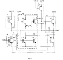
- Fig. 15 shows another exemplary circuit implementation of the shift register unit for a display device of the present invention.
- the reset module 54 further comprises an output reset transistor T4.
- a connection manner of the output reset transistor T4 is the same as that in Fig. 11 , and thus no further description is given herein.
- the fifth control signal of the fifth control signal end CON5 is at the high level, and the output reset transistor T4 is turned on to pull down the output end OUT to the low power supply voltage of the low power supply voltage end VSS.
- the driving capacity of the output end OUT can be enhanced by adding the reset transistor T4.
- the output end OUT can be pulled down to the low power supply voltage of the low power supply voltage end VSS faster by the cooperation of the output transistor T3 and the output reset transistor T4.
- Fig. 16 shows yet another exemplary circuit implementation of the shift register unit for a display device of the present invention.
- the pull-down module 56 further comprises a clock pull-down transistor T11. Connection manner of the clock pull-down transistor T11 is the same as that as shown in Fig. 11 , and thus no further description is given herein.
- the seventh control signal of the seventh control signal end CON7 is at the high level
- the clock pull-down transistor T11 is turned on to pull down the output end OUT to the low power supply voltage of the low power supply voltage end VSS.
- the driving capacity of the output end OUT can be enhanced by adding the clock pull-down transistor T11, and the output end OUT can be pulled down to the low power supply voltage of the low power supply voltage end VSS faster through cooperation of the output transistor T3 and the clock pull-down transistor T11.
- Fig. 17 shows a schematic block diagram of the shift register unit for a display device of the present invention.
- the shift register comprises multiple shift register units connected in cascades, each of which can be as shown in Fig. 13 .
- the shift register unit is connected with a start input signal end STV, a first clock signal end CLK1, a second clock signal end CLK2, a third clock signal end CLK1B and a fourth clock signal end CLK2B, a first pulse signal end CK_CP2, and a second pulse signal end CK_CP2.
- Periods of a first clock signal at the first clock signal end CLK1, a second clock signal at the second clock signal end CLK2, a third clock signal at the third clock signal end and a fourth clock signal at the fourth clock signal end CLK2B are the first period, and the second clock signal is prolonged 1/4 of the first period than the first clock signal, the third clock signal is prolonged 1/4 of the first period than the second clock signal, and the fourth clock signal is prolonged 1/4 of the first period than the third clock signal.
- Periods of a first pulse signal at the first pulse signal end CK_CP1 and a second pulse signal at the second pulse signal end CK_CP2 are second periods, and the second pulse signal is prolonged 1/2 of the second period than the first pulse signal, duty ratios of the first pulse signal and the second pulse signal are the same and smaller than or equal to 1/2, and the second period is 1/2 of the first period.
- Input ends INPUT of first and second stages of shift register units are connected with an initial input signal end STV to receive an initial input signal, an input end of a (2j+1)-th stage of shift register unit is connected with an output end of a (2j-1)-th stage of shift register unit, and an input end of a (2j+2)-th stage of shift register unit is connected with an output end of a (2j)-th stage of shift register unit, where j is a positive integer greater than or equal to 1.
- a first control signal end of a (4i+1)-th stage of shift register unit is connected with the first clock signal end CLK1, a second control signal end thereof is connected with an output end of a (4i+2)-th stage of shift register unit, a third control signal is connected with the first pulse signal end, and a fourth control signal end thereof is connected with an output end of a (4i+4)-th stage of shift register unit, and a sixth control signal end thereof is connected with the fourth clock signal end CLK2B, where i is an integer greater than or equal to 0.
- a first control signal end of a (4i+2)-th stage of shift register unit is connected with the second clock signal end CLK2, a second control signal end thereof is connected with an output end of a (4i+3)-th stage of shift register unit, a fourth control signal thereof is connected with an output end of a (4i+5)-th stage of shift register unit, and a sixth control signal end thereof is connected with a first clock signal end CLK1.
- a first control signal end of a (4i+3)-th stage of shift register unit is connected with the third clock signal end CLK1B, a second control signal end thereof is connected with an output end of a (4i+4)-th stage of shift register unit, a fourth control signal end thereof is connected with an output end of a (4i+6)-th stage of shift register unit, and a sixth control signal thereof is connected with the second clock signal end CLK2.
- a first control signal end of a (4i+4)-th stage of shift register unit is connected with the fourth clock signal end CLK2B, a second control signal end thereof is connected with an output end of a (4i+5)-th stage of shift register unit, a fourth control signal end thereof is connected with an output end of a (4i+7)-th stage of shift register unit, and a sixth control signal end thereof is connected with the third clock signal end CLK1B.
- each shift register unit being the shift register unit as shown in Fig. 15 .
- a fifth control signal end of the (2j-1)-th stage of shift register unit is connected with an output end of the (2j+1)-th stage of shift register unit, and a fifth control signal end of the (2j)-th stage of shift register unit is connected with an output end of the (2j+2)-th stage of shift register unit, where j is an integer greater than or equal to 1.
- each shift register unit being the shift register unit as shown in Fig. 16
- a seventh control signal end of the (4i+1)-th stage of shift register unit is connected with the third clock signal end CLK1B
- a seventh control signal end of the (4i+2)-th stage of shift register unit is connected with the fourth clock signal end CLK2B
- a seventh control signal end of the (4i+3)-th stage of shift register unit is connected with the first clock signal end CLK1
- a seventh control signal end of the (4i+1)-th stage of shift register unit is connected with the second clock signal end CLK2, where i is an integer greater than or equal to 0.
- the above respective transistors are N type thin film transistors, and the first electrode can be a drain, the second electrode can be a source, the effective control level, the effective pull-up level and the effective pull-down level are the high level, the ineffective control level, the ineffective pull-up level and the ineffective pull-down level are the low level.
- the respective transistors can be P type thin film transistors
- the first electrode can be a source
- the second electrode can be a drain
- the effective control level, the effective pull-up level and the effective pull-down level are the low level
- the ineffective control level, the ineffective pull-up level and the ineffective pull-down level are the high level.
- the respective transistors can be any combination of the P type and N type thin film transistors.
- the shift register unit and the operation method for the shift register unit, and the shift register for a display device of the present invention can not only utilize the output transistor to realize resetting of the shift register unit but also enhance speed of resetting the output end by the output transistor, so that the reset time of the shift register unit is reduced, which is helpful to enhance resolution of the display device and narrow frame of the display device.
Landscapes
- Engineering & Computer Science (AREA)
- Physics & Mathematics (AREA)
- Computer Hardware Design (AREA)
- General Physics & Mathematics (AREA)
- Theoretical Computer Science (AREA)
- Power Engineering (AREA)
- Microelectronics & Electronic Packaging (AREA)
- Control Of Indicators Other Than Cathode Ray Tubes (AREA)
- Shift Register Type Memory (AREA)
- Liquid Crystal Display Device Control (AREA)
Claims (11)
- Anzeigevorrichtung mit einem Schieberegister mit einer Schieberegistereinheit, wobei die Schieberegistereinheit aufweist:ein Eingangsmodul (51), von dem ein erstes Ende mit einem Eingangsende (INPUT) der Schieberegistereinheit verbunden ist, um ein Eingangssignal von dem Eingangsende (INPUT) zu empfangen, und ein zweites Ende mit einem Pull-up-Knoten (PU) verbunden ist, und das konfiguriert ist, um ein empfangenes Eingangssignal an den Pull-up-Knoten (PU) zu übertragen;ein Ausgabemodul (52), von dem ein erstes Ende mit dem Pull-up-Knoten (PU) verbunden ist, ein zweites Ende mit einem ersten Steuersignalende (CON1) verbunden ist und ein drittes Ende mit einem Ausgangsende (OUT) der Schieberegistereinheit verbunden ist, und das konfiguriert ist, um ein erstes Steuersignal des ersten Steuersignalendes an das Ausgangsende (OUT) auszugeben, wenn ein Pull-up-Signal an dem Pull-up-Knoten (PU) einen effektiven Pull-up-Pegel aufweist;ein Kopplungsmodul (53), von dem ein erstes Ende mit einem zweiten Steuersignalende (CON2) verbunden ist, ein zweites Ende mit dem Pull-up-Knoten (PU) verbunden ist und ein drittes Ende mit einem dritten Steuersignalende (CON3) verbunden ist, und das konfiguriert ist, um das Pull-up-Signal an dem Pull-up-Knoten (PU) gemäß einem zweiten Steuersignal des zweiten Steuersignalendes (CON2) und einem dritten Steuersignal des dritten Steuersignalendes (CON3) über eine Spannungskopplung zu steuern, wobei das Kopplungsmodul (53) einen Kopplungstransistor (Tc) aufweist, dessen Gate mit dem zweiten Steuersignalende (CON2) verbunden ist, und eine erste Elektrode mit dem dritten Steuersignalende (CON3) verbunden ist; und einen ersten Kondensator (C1), dessen erstes Ende mit einer zweiten Elektrode des Kopplungstransistors (Tc) verbunden ist und dessen zweites Ende mit dem Pull-up-Knoten (PU) verbunden ist, und wobei das Kopplungsmodul (53) konfiguriert ist, um das Pull-up-Signal an dem Pull-up-Knoten (PU) durch Spannungskopplung von der ersten Kopplungsspannung auf die zweite Kopplungsspannung springen zu lassen, wenn das zweite Steuersignal des zweiten Steuersignalendes (CON2) auf einem gültigen Steuerpegel ist und das dritte Steuersignal des dritten Steuersignalendes (CON3) von dem ersten Pegel auf den zweiten Pegel springt,dadurch gekennzeichnet, dass die Anzeigevorrichtung eingerichtet ist, das erste Steuersignal, das zweite Steuersignal und das dritte Steuersignal so zu steuern, dass das erste Steuersignal ein erstes Taktsignal ist, das von einem ersten Taktsignalende bereitgestellt wird, und eine Periode des ersten Steuersignals die erste Periode ist, eine Periode des dritten Steuersignals eine zweite Periode ist, die zweite Periode 1/2 der ersten Periode ist, ein Tastverhältnis des dritten Steuersignals kleiner als oder gleich 1/2 ist, und das dritte Steuersignal auf einem gültigen Steuerpegel sowohl bei einer Anstiegsflanke als auch bei einer Abstiegsflanke des ersten Steuersignals ist, um einen Gate-Impuls am Ausgangsende (OUT) zu erhalten, wobei der Gate-Impuls eine Impulsperiode hat, die 1/2 der ersten Periode ist, das zweite Steuersignal eine Wellenform hat, die dem Gate-Impuls am Ausgangsende (OUT) entspricht, aber um 1/4 der ersten Periode verzögert ist, verglichen mit dem Ausgangssignal am Ausgangsende (OUT) der Schieberegistereinheit.
- Anzeigevorrichtung nach Anspruch 1, die ferner aufweist:ein Rücksetzmodul (54), dessen erstes Ende mit einem vierten Steuersignalende (CON4) verbunden ist, dessen zweites Ende mit dem Pull-up-Knoten (PU) verbunden ist und dessen drittes Ende mit einem Ende für eine niedrige Versorgungsspannung (VSS) verbunden ist, und wobei das Rücksetzmodul (54) konfiguriert ist, um das Pull-up-Signal an dem Pull-up-Knoten (PU) auf eine niedrige Versorgungsspannung des Endes für eine niedrige Versorgungsspannung (VSS) herunterzuziehen, wenn ein viertes Steuersignal des vierten Steuersignalendes (CON4) auf einem gültigen Steuerpegel ist,wobei das vierte Steuersignal um 3/4 der ersten Periode verzögert ist, verglichen mit dem Ausgangssignal am Ausgangsende (OUT) der Schieberegistereinheit.
- Anzeigevorrichtung nach Anspruch 2, wobeiein viertes Ende des Rücksetzmoduls (54) mit einem fünften Steuersignalende (CON5) und ein fünftes Ende desselben mit dem Ausgangsende (OUT) verbunden ist und das Rücksetzmodul (54) ferner konfiguriert ist, um das Ausgangssignal am Ausgangsende (OUT) auf die niedrige Stromversorgungsspannung des niedrigen Stromversorgungsspannungsendes (VSS) herunterzuziehen, wenn ein fünftes Steuersignal des fünften Steuersignalendes (CON5) auf einem gültigen Steuerpegel ist, unddas fünfte Steuersignal im Vergleich zum Ausgangssignal am Ausgangsende (OUT) der Schieberegistereinheit um die Hälfte der ersten Periode verzögert ist.
- Anzeigevorrichtung nach Anspruch 2, die ferner aufweist:ein Pull-Down-Steuermodul (55), dessen erstes Ende mit einem sechsten Steuersignalende (CON6) verbunden ist, dessen zweites Ende mit dem Pull-Up-Knoten (PU) verbunden ist und dessen drittes Ende mit einem Pull-Down-Modus (PD) verbunden ist, und das Pull-Down-Steuermodul konfiguriert ist, um ein Pull-Down-Signal an dem Pull-Down-Knoten (PD) auf einem ungültigen Steuerpegel zu erzeugen, wenn das Pull-Up-Signal an dem Pull-Up-Knoten (PU) auf einem gültigen Steuerpegel ist, und um ein Pull-Down-Signal an dem Pull-Down-Knoten (PD) auf einem gültigen Steuerpegel zu erzeugen, wenn das Pull-Up-Signal an dem Pull-Up-Knoten (PU) auf einem ungültigen Steuerpegel ist und wenn ein sechstes Steuersignal des sechsten Steuersignalendes (CON6) auf einem gültigen Steuerpegel ist; undein Pull-Down-Modul (56), von dem ein erstes Ende mit dem Pull-Down-Knoten (PD) verbunden ist, ein zweites Ende mit dem Ausgangsende verbunden ist, ein drittes Ende mit dem Pull-Up-Knoten (PU) verbunden ist und ein viertes Ende mit dem Ende (VSS) für die niedrige Stromversorgungsspannung verbunden ist und konfiguriert ist, um das Ausgangsende und den Pull-Up-Knoten (PU) auf die niedrige Stromversorgungsspannung des Endes (VSS) für die niedrige Stromversorgungsspannung herunterzuziehen, wenn das Pull-Down-Signal an dem Pull-Down-Knoten (PD) auf einem gültigen Pull-Down-Pegel ist,wobei das sechste Steuersignal im Vergleich zum ersten Steuersignal um 3/4 der ersten Periode verzögert ist.
- Anzeigevorrichtung nach Anspruch 4, wobeiein fünftes Ende des Pull-Down-Moduls (56) mit einem siebten Steuersignalende (CON7) verbunden ist und das Pull-Down-Modul (56) ferner so konfiguriert ist, dass es das Ausgangsende (OUT) auf die niedrige Stromversorgungsspannung des niedrigenStromversorgungsspannungsendes (VSS) herunterzieht, wenn sich ein siebtes Steuersignal des siebten Steuersignalendes (CON7) auf einem gültigen Steuerpegel befindet, wobei das siebte Steuersignal im Vergleich zum ersten Steuersignal um 1/2 der ersten Periode verzögert ist.
- Anzeigevorrichtung nach Anspruch 1, wobeidas Eingangsmodul (51) einen Eingangstransistor (T1) aufweist, dessen Gate und erste Elektrode mit dem Eingangsende (INPUT) verbunden ist, und dessen zweite Elektrode mit dem Pull-up-Knoten (PU) verbunden ist; unddas Ausgangsmodul (52) einen Ausgangstransistor (T3) und einen zweiten Kondensator (C2) aufweist, wobei ein Gate des Ausgangstransistors (T3) und ein erstes Ende des zweiten Kondensators (C2) mit dem Pull-up-Knoten (PU) verbunden sind, eine erste Elektrode des Ausgangstransistors (T3) mit dem ersten Steuersignalende (CON1) verbunden ist und eine zweite Elektrode des Ausgangstransistors (T3) und ein zweites Ende des zweiten Kondensators (C2) mit dem Ausgangsende (OUT) verbunden sind.
- Anzeigevorrichtung nach Anspruch 3, wobeidas Rücksetzmodul (54) einen Knoten-Rücksetztransistor (T2) und einen Ausgangs-Rücksetztransistor (T4) aufweist, ein Gate des Knoten-Rücksetztransistors (T2) mit dem vierten Steuersignalende (CON4) verbunden ist, eine erste Elektrode desselben mit dem Pull-up-Knoten (PU) verbunden ist und eine zweite Elektrode desselben mit dem Ende der niedrigen Stromversorgungsspannung (VSS) verbunden ist; undein Gate des Ausgangsrücksetztransistors (T4) mit dem fünften Transistorsignalende (CON5) verbunden ist, eine erste Elektrode davon mit dem Ausgangsende (OUT) verbunden ist und eine zweite Elektrode davon mit dem Ende der niedrigen Stromversorgungsspannung (VSS) verbunden ist.
- Anzeigevorrichtung nach Anspruch 5, wobeidas Pull-Down-Steuermodul (55) einen ersten Pull-Down-Steuertransistor (T9), einen zweiten Pull-Down-Steuertransistor (T10), einen dritten Pull-Down-Steuertransistor (T7) und einen vierten Pull-Down-Steuertransistor (T8) aufweist; und das Pull-Down-Modul (56) einen Knoten-Pull-Down-Transistor (T5) und einen Ausgangs-Pull-Down-Transistor (T6) aufweist;ein Gate und eine erste Elektrode des ersten Pull-Down-Steuertransistors (T9) mit dem sechsten Steuersignalende (CON6) verbunden ist, und eine zweite Elektrode davon mit einem Pull-Down-Steuerknoten (PD_CN) verbunden ist;ein Gate des zweiten Pull-Down-Steuertransistors (T10) mit dem Pull-Up-Knoten (PU) verbunden ist, eine erste Elektrode desselben mit dem Pull-Down-Steuerknoten (PD_CN) verbunden ist und eine zweite Elektrode desselben mit dem Ende der niedrigen Versorgungsspannung (VSS) verbunden ist;ein Gate des dritten Pull-Down-Steuertransistors (T7) mit dem Pull-Down-Steuerknoten (PD_CN) verbunden ist, eine erste Elektrode davon mit dem sechsten Steuersignalende (CN6) verbunden ist, und eine zweite Elektrode davon mit dem Pull-Down-Knoten (PD) verbunden ist;ein Gate des vierten Pull-Down-Steuertransistors (T8) mit dem Pull-Up-Knoten (PU) verbunden ist, eine erste Elektrode davon mit dem Pull-Down-Knoten (PD) verbunden ist und eine zweite Elektrode davon mit dem Ende der niedrigen Versorgungsspannung (VSS) verbunden ist; unddie Gates des Knoten-Pull-Down-Transistors (T5) und des Ausgangs-Pull-Down-Transistors (T6) mit dem Pull-Down-Knoten (PD) verbunden sind und deren zweite Elektroden mit dem Ende der niedrigen Stromversorgungsspannung (VSS) verbunden sind, eine erste Elektrode des Knoten-Pull-Down-Transistors (T5) mit dem Pull-Up-Knoten (PU) verbunden ist und eine erste Elektrode des Ausgangs-Pull-Down-Transistors (T6) mit dem Ausgangsende (OUT) verbunden ist.
- Anzeigevorrichtung nach Anspruch 1-8, bei der das Schieberegister mehrere in Kaskaden geschaltete Schieberegistereinheiten aufweist, wobeidie Eingangsenden der ersten und zweiten Stufen der Schieberegistereinheiten ein anfängliches Eingangssignal (STV) empfangen, ein Eingangsende einer (2j+1)-ten Stufe der Schieberegistereinheit mit einem Ausgangsende (OUT) einer (2j-l)-ten Stufe der Schieberegistereinheit verbunden ist, und ein Eingangsende einer (2j+2)-ten Stufe der Schieberegistereinheit mit einem Ausgangsende (OUT) einer 2j-ten Stufe der Schieberegistereinheit verbunden ist, wobei j eine ganze Zahl größer oder gleich 1 ist;ein erstes Steuersignalende (CON1) einer (4i+1)-ten Stufe der Schieberegistereinheit ist mit einem ersten Taktsignalende (CLK1) verbunden, und ein zweites Steuersignalende (CON2) davon ist mit einem Ausgangsende (OUT) einer (4i+2)-ten Stufe der Schieberegistereinheit verbunden, wobei i eine ganze Zahl größer oder gleich 0 ist;ein erstes Steuersignalende (CON1) der (4i+2)-ten Stufe der Schieberegistereinheit ist mit einem zweiten Taktsignalende (CLK2) verbunden, und ein zweites Steuersignalende (CON2) davon ist mit einem Ausgangsende (OUT) einer (4i+3)-ten Stufe der Schieberegistereinheit verbunden;ein erstes Steuersignalende (CON1) der (4i+3)-ten Stufe der Schieberegistereinheit mit einem dritten Taktsignalende (CLK1B) verbunden ist, und ein zweites Steuersignalende (CON2) davon mit einem Ausgangsende (OUT) einer (4i+4)-ten Stufe der Schieberegistereinheit verbunden ist;ein erstes Steuersignalende (CON1) der (4i+4)-ten Stufe der Schieberegistereinheit mit einem vierten Taktsignalende (CLK2B) verbunden ist, und ein zweites Steuersignalende (CON2) davon mit einem Ausgangsende (OUT) einer (4i+5)-ten Stufe der Schieberegistereinheit verbunden ist,wobei Perioden eines ersten Taktsignals an dem ersten Taktsignalende (CLK1), eines zweiten Taktsignals an dem zweiten Taktsignalende (CLK2), eines dritten Taktsignals an dem dritten Taktsignalende (CLK1B) und eines vierten Taktsignals an dem vierten Taktsignalende (CLK2B) die erste Periode sind, und das zweite Taktsignal um 1/4 der ersten Periode gegenüber dem ersten Taktsignal verzögert ist, das dritte Taktsignal um 1/4 der ersten Periode gegenüber dem zweiten Taktsignal verzögert ist, und das vierte Taktsignal um 1/4 der ersten Periode gegenüber dem dritten Taktsignal verzögert ist.
- Anzeigevorrichtung nach Anspruch 9, wobeidas dritte Steuersignalende (CON3) der (2j-1)-ten Stufe der Schieberegistereinheit mit einem ersten Impulssignalende (CK_CP1) verbunden ist; ein drittes Steuersignalende (CON3) der 2j-ten Stufe der Schieberegistereinheit mit einem zweiten Impulssignalende (CK_CP2) verbunden ist, undPerioden eines ersten Impulssignals am ersten Impulssignalende (CK_CP1) und eines zweiten Impulssignals am zweiten Impulssignalende (CK_CP2) die zweite Periode ist, und das zweite Impulssignal um 1/2 der zweiten Periode im Vergleich zum ersten Impulssignal verzögert ist, die Tastverhältnisse des ersten Impulssignals und des zweiten Impulssignals gleich und kleiner oder gleich 1/2 sind und die zweite Periode 1/2 der ersten Periode ist.
- Betriebsverfahren für die Anzeigevorrichtung nach Anspruch 1-8, wobei das Verfahren aufweist:in dem Fall, dass das Ausgangssignal am Ausgangsende (OUT) des Ausgangsmoduls (52) auf einem hohen Pegel ist, Anheben des Pull-up-Signals am Pull-up-Knoten (PU) durch das Kopplungsmodul (53) von einer ersten Pull-up-Spannung auf eine zweite Pull-up-Spannung durch Spannungskopplung gemäß dem zweiten Steuersignal des zweiten Steuersignalendes (CN2) und einem dritten Steuersignal des dritten Steuersignalendes (CON3); undin dem Fall, dass das erste Steuersignal des ersten Steuersignalendes (CON1) von dem hohen Pegel auf einen niedrigen Pegel springt, ein Pull-up-Signal der zweiten Pull-up-Spannung an dem Pull-up-Knoten (PU), das das Ausgangsmodul (52) dazu bringt, das Ausgangsende (OUT) auf den niedrigen Pegel des ersten Steuersignals herunterzuziehen,wobei das Ausgangsmodul (52) das erste Steuersignal an das Ausgangsende (OUT) ausgibt, wenn das Pull-up-Signal an dem Pull-up-Knoten (PU) in der ersten Pull-up-Spannung und der zweiten Pull-up-Spannung liegt.
Applications Claiming Priority (2)
| Application Number | Priority Date | Filing Date | Title |
|---|---|---|---|
| CN201510649786.4A CN105161134B (zh) | 2015-10-09 | 2015-10-09 | 移位寄存器单元及其操作方法、移位寄存器 |
| PCT/CN2016/101107 WO2017059791A1 (zh) | 2015-10-09 | 2016-09-30 | 移位寄存器单元及其操作方法、移位寄存器 |
Publications (3)
| Publication Number | Publication Date |
|---|---|
| EP3361479A1 EP3361479A1 (de) | 2018-08-15 |
| EP3361479A4 EP3361479A4 (de) | 2019-10-30 |
| EP3361479B1 true EP3361479B1 (de) | 2022-06-01 |
Family
ID=54801962
Family Applications (1)
| Application Number | Title | Priority Date | Filing Date |
|---|---|---|---|
| EP16853096.2A Active EP3361479B1 (de) | 2015-10-09 | 2016-09-30 | Anzeigegerät mit schieberegister und betriebsverfahren dafür |
Country Status (4)
| Country | Link |
|---|---|
| US (1) | US10049762B2 (de) |
| EP (1) | EP3361479B1 (de) |
| CN (1) | CN105161134B (de) |
| WO (1) | WO2017059791A1 (de) |
Families Citing this family (17)
| Publication number | Priority date | Publication date | Assignee | Title |
|---|---|---|---|---|
| CN105161134B (zh) | 2015-10-09 | 2018-10-23 | 京东方科技集团股份有限公司 | 移位寄存器单元及其操作方法、移位寄存器 |
| TWI607450B (zh) * | 2016-12-30 | 2017-12-01 | 友達光電股份有限公司 | 移位暫存器與採用其之閘極驅動電路 |
| CN107248401B (zh) * | 2017-08-08 | 2020-04-03 | 京东方科技集团股份有限公司 | Goa电路及其驱动方法、显示装置 |
| CN109545156B (zh) * | 2017-09-21 | 2020-06-30 | 京东方科技集团股份有限公司 | 移位寄存器单元、栅极驱动电路、显示装置以及驱动方法 |
| CN107424554B (zh) * | 2017-09-26 | 2020-06-02 | 京东方科技集团股份有限公司 | 移位寄存器单元及其驱动方法、栅极驱动电路、显示装置 |
| CN110021259B (zh) | 2018-03-23 | 2020-12-22 | 京东方科技集团股份有限公司 | 电源电压提供电路、方法、显示基板和显示装置 |
| CN108806628B (zh) * | 2018-06-21 | 2021-01-22 | 京东方科技集团股份有限公司 | 移位寄存器单元及其驱动方法、栅极驱动电路及显示装置 |
| CN108806583B (zh) | 2018-07-05 | 2020-12-01 | 京东方科技集团股份有限公司 | 移位寄存器单元、驱动方法、移位寄存器和显示装置 |
| CN108831395B (zh) * | 2018-07-17 | 2020-09-04 | 惠科股份有限公司 | 显示装置及移位暂存电路 |
| CN109935209B (zh) * | 2018-07-18 | 2021-02-02 | 京东方科技集团股份有限公司 | 移位寄存器单元、栅极驱动电路、显示装置及驱动方法 |
| CN109064993B (zh) * | 2018-11-06 | 2020-01-21 | 合肥京东方光电科技有限公司 | 移位寄存器及其驱动方法、栅极驱动电路和显示装置 |
| CN111369927B (zh) * | 2020-03-23 | 2022-04-08 | 武汉天马微电子有限公司 | 移位寄存器及其控制方法、显示面板和显示装置 |
| CN111326096A (zh) * | 2020-04-07 | 2020-06-23 | 武汉华星光电技术有限公司 | Goa电路及显示面板 |
| CN111883075A (zh) | 2020-07-28 | 2020-11-03 | 北海惠科光电技术有限公司 | 面板驱动电路、方法及显示装置 |
| CN112687230B (zh) | 2021-01-29 | 2022-06-10 | 云谷(固安)科技有限公司 | 移位寄存器、栅极驱动电路和显示面板 |
| CN114333701B (zh) * | 2022-01-10 | 2023-03-28 | 信利(仁寿)高端显示科技有限公司 | 一种栅极驱动电路及方法 |
| CN116844458A (zh) * | 2023-07-26 | 2023-10-03 | 京东方科技集团股份有限公司 | 一种驱动电路及其驱动方法、显示装置 |
Family Cites Families (22)
| Publication number | Priority date | Publication date | Assignee | Title |
|---|---|---|---|---|
| GB0417132D0 (en) * | 2004-07-31 | 2004-09-01 | Koninkl Philips Electronics Nv | A shift register circuit |
| CN102012591B (zh) * | 2009-09-04 | 2012-05-30 | 北京京东方光电科技有限公司 | 移位寄存器单元及液晶显示器栅极驱动装置 |
| JP5419762B2 (ja) * | 2010-03-18 | 2014-02-19 | 三菱電機株式会社 | シフトレジスタ回路 |
| JP5420072B2 (ja) * | 2010-05-24 | 2014-02-19 | シャープ株式会社 | シフトレジスタ |
| TWI406503B (zh) * | 2010-12-30 | 2013-08-21 | Au Optronics Corp | 移位暫存器電路 |
| CN102654982B (zh) | 2011-05-16 | 2013-12-04 | 京东方科技集团股份有限公司 | 移位寄存器单元电路、移位寄存器、阵列基板及液晶显示器 |
| CN104464645B (zh) * | 2012-07-30 | 2017-04-05 | 京东方科技集团股份有限公司 | 移位寄存器和显示装置 |
| CN103632641B (zh) * | 2012-08-22 | 2016-01-20 | 瀚宇彩晶股份有限公司 | 液晶显示器及其移位寄存装置 |
| TWI505245B (zh) * | 2012-10-12 | 2015-10-21 | Au Optronics Corp | 移位暫存器 |
| CN103366704B (zh) * | 2013-07-10 | 2015-08-19 | 京东方科技集团股份有限公司 | 一种移位寄存器单元及栅极驱动电路、显示装置 |
| TWI514361B (zh) * | 2013-10-03 | 2015-12-21 | Au Optronics Corp | 閘極驅動電路 |
| TWI505276B (zh) * | 2014-02-13 | 2015-10-21 | Au Optronics Corp | 移位暫存電路及移位暫存器 |
| US9997112B2 (en) * | 2014-03-10 | 2018-06-12 | Lg Display Co., Ltd. | Display device |
| CN104575436B (zh) * | 2015-02-06 | 2017-04-05 | 京东方科技集团股份有限公司 | 移位寄存器单元、栅极驱动电路及显示装置 |
| CN104616616B (zh) | 2015-02-12 | 2017-12-15 | 京东方科技集团股份有限公司 | 栅极驱动电路及其驱动方法、阵列基板、显示装置 |
| CN104616617B (zh) * | 2015-03-09 | 2017-03-22 | 京东方科技集团股份有限公司 | 移位寄存器及其驱动方法、栅极驱动电路、显示装置 |
| CN104766575B (zh) * | 2015-04-07 | 2017-10-17 | 深圳市华星光电技术有限公司 | 一种goa电路及液晶显示器 |
| CN104700769B (zh) * | 2015-04-09 | 2017-03-15 | 京东方科技集团股份有限公司 | 移位寄存器单元、栅极驱动装置以及显示装置 |
| CN104809973B (zh) | 2015-04-09 | 2017-10-31 | 北京大学深圳研究生院 | 一种可适应负阈值电压的移位寄存器及其单元 |
| KR102342327B1 (ko) * | 2015-04-30 | 2021-12-24 | 삼성디스플레이 주식회사 | 표시장치 |
| CN204966057U (zh) * | 2015-10-09 | 2016-01-13 | 京东方科技集团股份有限公司 | 移位寄存器单元以及移位寄存器 |
| CN105161134B (zh) | 2015-10-09 | 2018-10-23 | 京东方科技集团股份有限公司 | 移位寄存器单元及其操作方法、移位寄存器 |
-
2015
- 2015-10-09 CN CN201510649786.4A patent/CN105161134B/zh active Active
-
2016
- 2016-09-30 US US15/532,343 patent/US10049762B2/en active Active
- 2016-09-30 WO PCT/CN2016/101107 patent/WO2017059791A1/zh not_active Ceased
- 2016-09-30 EP EP16853096.2A patent/EP3361479B1/de active Active
Also Published As
| Publication number | Publication date |
|---|---|
| US10049762B2 (en) | 2018-08-14 |
| WO2017059791A1 (zh) | 2017-04-13 |
| CN105161134B (zh) | 2018-10-23 |
| US20170345515A1 (en) | 2017-11-30 |
| EP3361479A4 (de) | 2019-10-30 |
| CN105161134A (zh) | 2015-12-16 |
| EP3361479A1 (de) | 2018-08-15 |
Similar Documents
| Publication | Publication Date | Title |
|---|---|---|
| EP3361479B1 (de) | Anzeigegerät mit schieberegister und betriebsverfahren dafür | |
| US9478310B2 (en) | Shift register unit, gate driving circuit and method, display apparatus | |
| EP3214616B1 (de) | Goa-einheit und ansteuerungsverfahren, goa-schaltung und anzeigevorrichtung | |
| US10775925B2 (en) | Shift register unit and method for driving the same, gate driving circuit and display apparatus | |
| US10607529B2 (en) | Shift register unit and driving method thereof, gate driving circuit and display apparatus | |
| US10964243B2 (en) | Shift register circuit and its driving method, gate driving circuit and its driving method, and display device | |
| US10540923B2 (en) | Shift register, method for driving same, gate driving circuit | |
| EP3041000B1 (de) | Schieberegistereinheit, schieberegister und anzeigevorrichtung | |
| US10043585B2 (en) | Shift register unit, gate drive device, display device, and control method | |
| JP2019537044A (ja) | 走査駆動回路および表示装置 | |
| KR101639496B1 (ko) | 시프트 레지스터, 게이트 구동 회로, 어레이 기판, 및 디스플레이 디바이스 | |
| CN104157252B (zh) | 一种移位寄存器、栅极驱动电路及显示装置 | |
| US10115335B2 (en) | Shift register unit and driving method thereof, gate driving circuit and display device | |
| US10096373B2 (en) | Shift register and driving method therefor, gate driver on array circuit and display device | |
| US10319324B2 (en) | Shift registers, driving methods, gate driving circuits and display apparatuses with reduced shift register output signal voltage switching time | |
| KR20170102134A (ko) | 게이트 구동 회로 및 이를 포함하는 표시 장치 | |
| CN104966503A (zh) | 一种栅极驱动电路及其驱动方法、电平移位器 | |
| US8971478B2 (en) | Shift register, signal line drive circuit, liquid crystal display device | |
| KR102040601B1 (ko) | 게이트 구동 회로 및 이를 포함하는 디스플레이 장치 | |
| CN108109575B (zh) | 栅极驱动电路和显示装置 | |
| CN204966057U (zh) | 移位寄存器单元以及移位寄存器 | |
| US11158224B2 (en) | Start signal generation circuit, driving method and display device | |
| CN119132235B (zh) | 发射脉冲生成电路及发射脉冲生成方法 | |
| US20210335309A1 (en) | Gate driver on array circuit |
Legal Events
| Date | Code | Title | Description |
|---|---|---|---|
| STAA | Information on the status of an ep patent application or granted ep patent |
Free format text: STATUS: THE INTERNATIONAL PUBLICATION HAS BEEN MADE |
|
| PUAI | Public reference made under article 153(3) epc to a published international application that has entered the european phase |
Free format text: ORIGINAL CODE: 0009012 |
|
| STAA | Information on the status of an ep patent application or granted ep patent |
Free format text: STATUS: REQUEST FOR EXAMINATION WAS MADE |
|
| 17P | Request for examination filed |
Effective date: 20170601 |
|
| AK | Designated contracting states |
Kind code of ref document: A1 Designated state(s): AL AT BE BG CH CY CZ DE DK EE ES FI FR GB GR HR HU IE IS IT LI LT LU LV MC MK MT NL NO PL PT RO RS SE SI SK SM TR |
|
| AX | Request for extension of the european patent |
Extension state: BA ME |
|
| DAV | Request for validation of the european patent (deleted) | ||
| DAX | Request for extension of the european patent (deleted) | ||
| RIC1 | Information provided on ipc code assigned before grant |
Ipc: G11C 19/28 20060101ALI20190507BHEP Ipc: G09G 3/20 20060101AFI20190507BHEP |
|
| REG | Reference to a national code |
Ref country code: DE Ref legal event code: R079 Ref document number: 602016072588 Country of ref document: DE Free format text: PREVIOUS MAIN CLASS: G11C0019280000 Ipc: G09G0003200000 |
|
| RIC1 | Information provided on ipc code assigned before grant |
Ipc: G09G 3/20 20060101AFI20190919BHEP Ipc: G11C 19/28 20060101ALI20190919BHEP |
|
| A4 | Supplementary search report drawn up and despatched |
Effective date: 20190926 |
|
| RIC1 | Information provided on ipc code assigned before grant |
Ipc: G11C 19/28 20060101ALI20190920BHEP Ipc: G09G 3/20 20060101AFI20190920BHEP |
|
| STAA | Information on the status of an ep patent application or granted ep patent |
Free format text: STATUS: EXAMINATION IS IN PROGRESS |
|
| 17Q | First examination report despatched |
Effective date: 20201013 |
|
| GRAP | Despatch of communication of intention to grant a patent |
Free format text: ORIGINAL CODE: EPIDOSNIGR1 |
|
| STAA | Information on the status of an ep patent application or granted ep patent |
Free format text: STATUS: GRANT OF PATENT IS INTENDED |
|
| INTG | Intention to grant announced |
Effective date: 20220215 |
|
| GRAS | Grant fee paid |
Free format text: ORIGINAL CODE: EPIDOSNIGR3 |
|
| GRAA | (expected) grant |
Free format text: ORIGINAL CODE: 0009210 |
|
| STAA | Information on the status of an ep patent application or granted ep patent |
Free format text: STATUS: THE PATENT HAS BEEN GRANTED |
|
| AK | Designated contracting states |
Kind code of ref document: B1 Designated state(s): AL AT BE BG CH CY CZ DE DK EE ES FI FR GB GR HR HU IE IS IT LI LT LU LV MC MK MT NL NO PL PT RO RS SE SI SK SM TR |
|
| REG | Reference to a national code |
Ref country code: GB Ref legal event code: FG4D |
|
| REG | Reference to a national code |
Ref country code: AT Ref legal event code: REF Ref document number: 1495932 Country of ref document: AT Kind code of ref document: T Effective date: 20220615 Ref country code: CH Ref legal event code: EP Ref country code: DE Ref legal event code: R096 Ref document number: 602016072588 Country of ref document: DE |
|
| REG | Reference to a national code |
Ref country code: IE Ref legal event code: FG4D |
|
| REG | Reference to a national code |
Ref country code: LT Ref legal event code: MG9D |
|
| REG | Reference to a national code |
Ref country code: NL Ref legal event code: MP Effective date: 20220601 |
|
| PG25 | Lapsed in a contracting state [announced via postgrant information from national office to epo] |
Ref country code: SE Free format text: LAPSE BECAUSE OF FAILURE TO SUBMIT A TRANSLATION OF THE DESCRIPTION OR TO PAY THE FEE WITHIN THE PRESCRIBED TIME-LIMIT Effective date: 20220601 Ref country code: NO Free format text: LAPSE BECAUSE OF FAILURE TO SUBMIT A TRANSLATION OF THE DESCRIPTION OR TO PAY THE FEE WITHIN THE PRESCRIBED TIME-LIMIT Effective date: 20220901 Ref country code: LT Free format text: LAPSE BECAUSE OF FAILURE TO SUBMIT A TRANSLATION OF THE DESCRIPTION OR TO PAY THE FEE WITHIN THE PRESCRIBED TIME-LIMIT Effective date: 20220601 Ref country code: HR Free format text: LAPSE BECAUSE OF FAILURE TO SUBMIT A TRANSLATION OF THE DESCRIPTION OR TO PAY THE FEE WITHIN THE PRESCRIBED TIME-LIMIT Effective date: 20220601 Ref country code: GR Free format text: LAPSE BECAUSE OF FAILURE TO SUBMIT A TRANSLATION OF THE DESCRIPTION OR TO PAY THE FEE WITHIN THE PRESCRIBED TIME-LIMIT Effective date: 20220902 Ref country code: FI Free format text: LAPSE BECAUSE OF FAILURE TO SUBMIT A TRANSLATION OF THE DESCRIPTION OR TO PAY THE FEE WITHIN THE PRESCRIBED TIME-LIMIT Effective date: 20220601 Ref country code: ES Free format text: LAPSE BECAUSE OF FAILURE TO SUBMIT A TRANSLATION OF THE DESCRIPTION OR TO PAY THE FEE WITHIN THE PRESCRIBED TIME-LIMIT Effective date: 20220601 Ref country code: BG Free format text: LAPSE BECAUSE OF FAILURE TO SUBMIT A TRANSLATION OF THE DESCRIPTION OR TO PAY THE FEE WITHIN THE PRESCRIBED TIME-LIMIT Effective date: 20220901 |
|
| REG | Reference to a national code |
Ref country code: AT Ref legal event code: MK05 Ref document number: 1495932 Country of ref document: AT Kind code of ref document: T Effective date: 20220601 |
|
| PG25 | Lapsed in a contracting state [announced via postgrant information from national office to epo] |
Ref country code: RS Free format text: LAPSE BECAUSE OF FAILURE TO SUBMIT A TRANSLATION OF THE DESCRIPTION OR TO PAY THE FEE WITHIN THE PRESCRIBED TIME-LIMIT Effective date: 20220601 Ref country code: PL Free format text: LAPSE BECAUSE OF FAILURE TO SUBMIT A TRANSLATION OF THE DESCRIPTION OR TO PAY THE FEE WITHIN THE PRESCRIBED TIME-LIMIT Effective date: 20220601 Ref country code: LV Free format text: LAPSE BECAUSE OF FAILURE TO SUBMIT A TRANSLATION OF THE DESCRIPTION OR TO PAY THE FEE WITHIN THE PRESCRIBED TIME-LIMIT Effective date: 20220601 |
|
| PG25 | Lapsed in a contracting state [announced via postgrant information from national office to epo] |
Ref country code: NL Free format text: LAPSE BECAUSE OF FAILURE TO SUBMIT A TRANSLATION OF THE DESCRIPTION OR TO PAY THE FEE WITHIN THE PRESCRIBED TIME-LIMIT Effective date: 20220601 |
|
| PG25 | Lapsed in a contracting state [announced via postgrant information from national office to epo] |
Ref country code: SM Free format text: LAPSE BECAUSE OF FAILURE TO SUBMIT A TRANSLATION OF THE DESCRIPTION OR TO PAY THE FEE WITHIN THE PRESCRIBED TIME-LIMIT Effective date: 20220601 Ref country code: SK Free format text: LAPSE BECAUSE OF FAILURE TO SUBMIT A TRANSLATION OF THE DESCRIPTION OR TO PAY THE FEE WITHIN THE PRESCRIBED TIME-LIMIT Effective date: 20220601 Ref country code: RO Free format text: LAPSE BECAUSE OF FAILURE TO SUBMIT A TRANSLATION OF THE DESCRIPTION OR TO PAY THE FEE WITHIN THE PRESCRIBED TIME-LIMIT Effective date: 20220601 Ref country code: PT Free format text: LAPSE BECAUSE OF FAILURE TO SUBMIT A TRANSLATION OF THE DESCRIPTION OR TO PAY THE FEE WITHIN THE PRESCRIBED TIME-LIMIT Effective date: 20221003 Ref country code: EE Free format text: LAPSE BECAUSE OF FAILURE TO SUBMIT A TRANSLATION OF THE DESCRIPTION OR TO PAY THE FEE WITHIN THE PRESCRIBED TIME-LIMIT Effective date: 20220601 Ref country code: CZ Free format text: LAPSE BECAUSE OF FAILURE TO SUBMIT A TRANSLATION OF THE DESCRIPTION OR TO PAY THE FEE WITHIN THE PRESCRIBED TIME-LIMIT Effective date: 20220601 Ref country code: AT Free format text: LAPSE BECAUSE OF FAILURE TO SUBMIT A TRANSLATION OF THE DESCRIPTION OR TO PAY THE FEE WITHIN THE PRESCRIBED TIME-LIMIT Effective date: 20220601 |
|
| PG25 | Lapsed in a contracting state [announced via postgrant information from national office to epo] |
Ref country code: IS Free format text: LAPSE BECAUSE OF FAILURE TO SUBMIT A TRANSLATION OF THE DESCRIPTION OR TO PAY THE FEE WITHIN THE PRESCRIBED TIME-LIMIT Effective date: 20221001 |
|
| REG | Reference to a national code |
Ref country code: DE Ref legal event code: R097 Ref document number: 602016072588 Country of ref document: DE |
|
| PG25 | Lapsed in a contracting state [announced via postgrant information from national office to epo] |
Ref country code: AL Free format text: LAPSE BECAUSE OF FAILURE TO SUBMIT A TRANSLATION OF THE DESCRIPTION OR TO PAY THE FEE WITHIN THE PRESCRIBED TIME-LIMIT Effective date: 20220601 |
|
| PLBE | No opposition filed within time limit |
Free format text: ORIGINAL CODE: 0009261 |
|
| STAA | Information on the status of an ep patent application or granted ep patent |
Free format text: STATUS: NO OPPOSITION FILED WITHIN TIME LIMIT |
|
| PG25 | Lapsed in a contracting state [announced via postgrant information from national office to epo] |
Ref country code: MC Free format text: LAPSE BECAUSE OF FAILURE TO SUBMIT A TRANSLATION OF THE DESCRIPTION OR TO PAY THE FEE WITHIN THE PRESCRIBED TIME-LIMIT Effective date: 20220601 Ref country code: DK Free format text: LAPSE BECAUSE OF FAILURE TO SUBMIT A TRANSLATION OF THE DESCRIPTION OR TO PAY THE FEE WITHIN THE PRESCRIBED TIME-LIMIT Effective date: 20220601 |
|
| REG | Reference to a national code |
Ref country code: CH Ref legal event code: PL |
|
| 26N | No opposition filed |
Effective date: 20230302 |
|
| GBPC | Gb: european patent ceased through non-payment of renewal fee |
Effective date: 20220930 |
|
| REG | Reference to a national code |
Ref country code: BE Ref legal event code: MM Effective date: 20220930 |
|
| PG25 | Lapsed in a contracting state [announced via postgrant information from national office to epo] |
Ref country code: SI Free format text: LAPSE BECAUSE OF FAILURE TO SUBMIT A TRANSLATION OF THE DESCRIPTION OR TO PAY THE FEE WITHIN THE PRESCRIBED TIME-LIMIT Effective date: 20220601 |
|
| PG25 | Lapsed in a contracting state [announced via postgrant information from national office to epo] |
Ref country code: LU Free format text: LAPSE BECAUSE OF NON-PAYMENT OF DUE FEES Effective date: 20220930 |
|
| PG25 | Lapsed in a contracting state [announced via postgrant information from national office to epo] |
Ref country code: LI Free format text: LAPSE BECAUSE OF NON-PAYMENT OF DUE FEES Effective date: 20220930 Ref country code: IE Free format text: LAPSE BECAUSE OF NON-PAYMENT OF DUE FEES Effective date: 20220930 Ref country code: FR Free format text: LAPSE BECAUSE OF NON-PAYMENT OF DUE FEES Effective date: 20220930 Ref country code: CH Free format text: LAPSE BECAUSE OF NON-PAYMENT OF DUE FEES Effective date: 20220930 |
|
| PG25 | Lapsed in a contracting state [announced via postgrant information from national office to epo] |
Ref country code: BE Free format text: LAPSE BECAUSE OF NON-PAYMENT OF DUE FEES Effective date: 20220930 |
|
| PG25 | Lapsed in a contracting state [announced via postgrant information from national office to epo] |
Ref country code: GB Free format text: LAPSE BECAUSE OF NON-PAYMENT OF DUE FEES Effective date: 20220930 |
|
| PG25 | Lapsed in a contracting state [announced via postgrant information from national office to epo] |
Ref country code: IT Free format text: LAPSE BECAUSE OF FAILURE TO SUBMIT A TRANSLATION OF THE DESCRIPTION OR TO PAY THE FEE WITHIN THE PRESCRIBED TIME-LIMIT Effective date: 20220601 |
|
| PG25 | Lapsed in a contracting state [announced via postgrant information from national office to epo] |
Ref country code: HU Free format text: LAPSE BECAUSE OF FAILURE TO SUBMIT A TRANSLATION OF THE DESCRIPTION OR TO PAY THE FEE WITHIN THE PRESCRIBED TIME-LIMIT; INVALID AB INITIO Effective date: 20160930 |
|
| PG25 | Lapsed in a contracting state [announced via postgrant information from national office to epo] |
Ref country code: CY Free format text: LAPSE BECAUSE OF FAILURE TO SUBMIT A TRANSLATION OF THE DESCRIPTION OR TO PAY THE FEE WITHIN THE PRESCRIBED TIME-LIMIT Effective date: 20220601 |
|
| PG25 | Lapsed in a contracting state [announced via postgrant information from national office to epo] |
Ref country code: MK Free format text: LAPSE BECAUSE OF FAILURE TO SUBMIT A TRANSLATION OF THE DESCRIPTION OR TO PAY THE FEE WITHIN THE PRESCRIBED TIME-LIMIT Effective date: 20220601 |
|
| PG25 | Lapsed in a contracting state [announced via postgrant information from national office to epo] |
Ref country code: TR Free format text: LAPSE BECAUSE OF FAILURE TO SUBMIT A TRANSLATION OF THE DESCRIPTION OR TO PAY THE FEE WITHIN THE PRESCRIBED TIME-LIMIT Effective date: 20220601 |
|
| PG25 | Lapsed in a contracting state [announced via postgrant information from national office to epo] |
Ref country code: MT Free format text: LAPSE BECAUSE OF FAILURE TO SUBMIT A TRANSLATION OF THE DESCRIPTION OR TO PAY THE FEE WITHIN THE PRESCRIBED TIME-LIMIT Effective date: 20220601 |
|
| PG25 | Lapsed in a contracting state [announced via postgrant information from national office to epo] |
Ref country code: BG Free format text: LAPSE BECAUSE OF FAILURE TO SUBMIT A TRANSLATION OF THE DESCRIPTION OR TO PAY THE FEE WITHIN THE PRESCRIBED TIME-LIMIT Effective date: 20220601 |
|
| PG25 | Lapsed in a contracting state [announced via postgrant information from national office to epo] |
Ref country code: BG Free format text: LAPSE BECAUSE OF FAILURE TO SUBMIT A TRANSLATION OF THE DESCRIPTION OR TO PAY THE FEE WITHIN THE PRESCRIBED TIME-LIMIT Effective date: 20220601 |
|
| PGFP | Annual fee paid to national office [announced via postgrant information from national office to epo] |
Ref country code: DE Payment date: 20250919 Year of fee payment: 10 |