EP3345218B1 - Integration of inductors with advanced-node system-on-chip (soc) using glass wafer with inductors and wafer-to-wafer joining - Google Patents
Integration of inductors with advanced-node system-on-chip (soc) using glass wafer with inductors and wafer-to-wafer joining Download PDFInfo
- Publication number
- EP3345218B1 EP3345218B1 EP16751137.7A EP16751137A EP3345218B1 EP 3345218 B1 EP3345218 B1 EP 3345218B1 EP 16751137 A EP16751137 A EP 16751137A EP 3345218 B1 EP3345218 B1 EP 3345218B1
- Authority
- EP
- European Patent Office
- Prior art keywords
- wafer
- inductor
- soc
- inductor wafer
- vias
- Prior art date
- Legal status (The legal status is an assumption and is not a legal conclusion. Google has not performed a legal analysis and makes no representation as to the accuracy of the status listed.)
- Active
Links
Images


Classifications
-
- H—ELECTRICITY
- H10—SEMICONDUCTOR DEVICES; ELECTRIC SOLID-STATE DEVICES NOT OTHERWISE PROVIDED FOR
- H10D—INORGANIC ELECTRIC SEMICONDUCTOR DEVICES
- H10D1/00—Resistors, capacitors or inductors
- H10D1/20—Inductors
-
- H—ELECTRICITY
- H10—SEMICONDUCTOR DEVICES; ELECTRIC SOLID-STATE DEVICES NOT OTHERWISE PROVIDED FOR
- H10W—GENERIC PACKAGES, INTERCONNECTIONS, CONNECTORS OR OTHER CONSTRUCTIONAL DETAILS OF DEVICES COVERED BY CLASS H10
- H10W44/00—Electrical arrangements for controlling or matching impedance
- H10W44/501—Inductive arrangements
-
- H—ELECTRICITY
- H10—SEMICONDUCTOR DEVICES; ELECTRIC SOLID-STATE DEVICES NOT OTHERWISE PROVIDED FOR
- H10W—GENERIC PACKAGES, INTERCONNECTIONS, CONNECTORS OR OTHER CONSTRUCTIONAL DETAILS OF DEVICES COVERED BY CLASS H10
- H10W90/00—Package configurations
- H10W90/401—Package configurations characterised by multiple insulating or insulated package substrates, interposers or RDLs
-
- H—ELECTRICITY
- H10—SEMICONDUCTOR DEVICES; ELECTRIC SOLID-STATE DEVICES NOT OTHERWISE PROVIDED FOR
- H10W—GENERIC PACKAGES, INTERCONNECTIONS, CONNECTORS OR OTHER CONSTRUCTIONAL DETAILS OF DEVICES COVERED BY CLASS H10
- H10W70/00—Package substrates; Interposers; Redistribution layers [RDL]
- H10W70/60—Insulating or insulated package substrates; Interposers; Redistribution layers
- H10W70/62—Insulating or insulated package substrates; Interposers; Redistribution layers characterised by their interconnections
- H10W70/63—Vias, e.g. via plugs
- H10W70/635—Through-vias
-
- H—ELECTRICITY
- H10—SEMICONDUCTOR DEVICES; ELECTRIC SOLID-STATE DEVICES NOT OTHERWISE PROVIDED FOR
- H10W—GENERIC PACKAGES, INTERCONNECTIONS, CONNECTORS OR OTHER CONSTRUCTIONAL DETAILS OF DEVICES COVERED BY CLASS H10
- H10W70/00—Package substrates; Interposers; Redistribution layers [RDL]
- H10W70/60—Insulating or insulated package substrates; Interposers; Redistribution layers
- H10W70/67—Insulating or insulated package substrates; Interposers; Redistribution layers characterised by their insulating layers or insulating parts
- H10W70/68—Shapes or dispositions thereof
- H10W70/685—Shapes or dispositions thereof comprising multiple insulating layers
-
- H—ELECTRICITY
- H10—SEMICONDUCTOR DEVICES; ELECTRIC SOLID-STATE DEVICES NOT OTHERWISE PROVIDED FOR
- H10W—GENERIC PACKAGES, INTERCONNECTIONS, CONNECTORS OR OTHER CONSTRUCTIONAL DETAILS OF DEVICES COVERED BY CLASS H10
- H10W72/00—Interconnections or connectors in packages
- H10W72/071—Connecting or disconnecting
- H10W72/072—Connecting or disconnecting of bump connectors
- H10W72/07231—Techniques
- H10W72/07236—Soldering or alloying
-
- H—ELECTRICITY
- H10—SEMICONDUCTOR DEVICES; ELECTRIC SOLID-STATE DEVICES NOT OTHERWISE PROVIDED FOR
- H10W—GENERIC PACKAGES, INTERCONNECTIONS, CONNECTORS OR OTHER CONSTRUCTIONAL DETAILS OF DEVICES COVERED BY CLASS H10
- H10W72/00—Interconnections or connectors in packages
- H10W72/20—Bump connectors, e.g. solder bumps or copper pillars; Dummy bumps; Thermal bumps
- H10W72/221—Structures or relative sizes
- H10W72/222—Multilayered bumps, e.g. a coating on top and side surfaces of a bump core
-
- H—ELECTRICITY
- H10—SEMICONDUCTOR DEVICES; ELECTRIC SOLID-STATE DEVICES NOT OTHERWISE PROVIDED FOR
- H10W—GENERIC PACKAGES, INTERCONNECTIONS, CONNECTORS OR OTHER CONSTRUCTIONAL DETAILS OF DEVICES COVERED BY CLASS H10
- H10W72/00—Interconnections or connectors in packages
- H10W72/20—Bump connectors, e.g. solder bumps or copper pillars; Dummy bumps; Thermal bumps
- H10W72/251—Materials
- H10W72/252—Materials comprising solid metals or solid metalloids, e.g. PbSn, Ag or Cu
-
- H—ELECTRICITY
- H10—SEMICONDUCTOR DEVICES; ELECTRIC SOLID-STATE DEVICES NOT OTHERWISE PROVIDED FOR
- H10W—GENERIC PACKAGES, INTERCONNECTIONS, CONNECTORS OR OTHER CONSTRUCTIONAL DETAILS OF DEVICES COVERED BY CLASS H10
- H10W72/00—Interconnections or connectors in packages
- H10W72/20—Bump connectors, e.g. solder bumps or copper pillars; Dummy bumps; Thermal bumps
- H10W72/251—Materials
- H10W72/255—Materials of outermost layers of multilayered bumps, e.g. material of a coating
-
- H—ELECTRICITY
- H10—SEMICONDUCTOR DEVICES; ELECTRIC SOLID-STATE DEVICES NOT OTHERWISE PROVIDED FOR
- H10W—GENERIC PACKAGES, INTERCONNECTIONS, CONNECTORS OR OTHER CONSTRUCTIONAL DETAILS OF DEVICES COVERED BY CLASS H10
- H10W90/00—Package configurations
- H10W90/701—Package configurations characterised by the relative positions of pads or connectors relative to package parts
- H10W90/721—Package configurations characterised by the relative positions of pads or connectors relative to package parts of bump connectors
- H10W90/724—Package configurations characterised by the relative positions of pads or connectors relative to package parts of bump connectors between a chip and a stacked insulating package substrate, interposer or RDL
-
- H—ELECTRICITY
- H10—SEMICONDUCTOR DEVICES; ELECTRIC SOLID-STATE DEVICES NOT OTHERWISE PROVIDED FOR
- H10W—GENERIC PACKAGES, INTERCONNECTIONS, CONNECTORS OR OTHER CONSTRUCTIONAL DETAILS OF DEVICES COVERED BY CLASS H10
- H10W90/00—Package configurations
- H10W90/701—Package configurations characterised by the relative positions of pads or connectors relative to package parts
- H10W90/721—Package configurations characterised by the relative positions of pads or connectors relative to package parts of bump connectors
- H10W90/728—Package configurations characterised by the relative positions of pads or connectors relative to package parts of bump connectors between a chip and a stacked discrete passive device, e.g. resistors, capacitors or inductors
Definitions
- Various embodiments described herein relate to integrated circuit devices, and more particularly, to integrated circuit devices with voltage regulators.
- Voltage regulators have been implemented in conventional dedicated power management integrated circuits (PMICs).
- PMICs dedicated power management integrated circuits
- a conventional PMIC which is separate from other integrated circuits on a circuit board, may have difficulty meeting the droop (transient) and power (efficiency) requirements of a modern multi-core application processor or communication processor, for example.
- Integrated voltage regulators may present several challenges in chip design and layout.
- passive components such as inductors and capacitors in voltage regulators may pose a design challenge, because passive components, such as inductors and capacitors, especially those with large inductance and capacitance values, typically have large form factors requiring large surface areas in a typical layout for a silicon SOC die.
- inductors in voltage regulators typically require very low resistances to minimize power losses in voltage regulation.
- such inductors may require thick metal traces on the SOC die in order to reduce the resistance values of the inductors.
- thick metal traces may not be feasible.
- conventional fabrication processes for integrating inductors as part of a voltage regulator on a silicon SOC die may require several additional masks, thereby increasing the cost of fabrication.
- US 2013/113448 A1 describes a structure and method of making a coil inductor on a semiconductor chip, on an interconnection device, or on a plurality of stacked semiconductor chips.
- US 2015/137342 A1 relates to systems and methods for providing
- Exemplary embodiments of the disclosure are directed to integrated circuit devices and methods of making the same.
- a device as set out in claim 1 and a method of making a device as set out in claim 7.
- Other aspects of the invention can be found in the dependent claims.
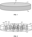
- FIG. 1 is a perspective view illustrating an embodiment of a system-on-chip (SOC) wafer 100 having a first surface 102 and a second surface 104 opposite each other.
- the SOC wafer 100 comprises a semiconductor wafer, such as a silicon wafer.
- the SOC wafer 100 may comprise a glass wafer, a quartz wafer, an organic wafer, or a wafer made of another material.
- the SOC wafer 100 is integrated with an inductor wafer on which one or more inductors are provided.
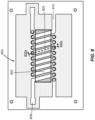
- FIG. 2 is a perspective view illustrating an embodiment of an inductor wafer 200 with a plurality of through vias 202a, 202b, 202c, ....
- the inductor wafer 200 has first and second surfaces 204 and 206 opposite each other, and the vias 202a, 202b, 202c, ... are formed through the first and second surfaces 204 and 206 of the inductor wafer 200.
- the inductor wafer 200 comprises a glass wafer.
- the inductor wafer 200 may comprise a quartz wafer, an organic wafer, or another type of low-loss dielectric material, to ensure that the inductor fabricated on the inductor wafer 200 has a low parasitic loss.
- the inductor wafer 200 may comprise a quartz wafer, an organic wafer, or another type of low-loss dielectric material, to ensure that the inductor fabricated on the inductor wafer 200 has a low parasitic loss.
- detailed structure of the conductors in the vias 202a, 202b, 202c, ... and the patterned conductive layers on the first and second surfaces 204 and 206 of the inductor wafer 200 which form one or more coils of an integrated inductor are not shown in the perspective view of FIG. 2 .
- Embodiments of the integrated inductor formed on the inductor wafer 200 will be described in further detail below with respect to FIGs. 4-7 and the top plan view of FIG. 8 .
- FIG. 3 is a perspective view illustrating an embodiment of face-to-face wafer-to-wafer bonding of the SOC wafer 100 and the inductor wafer 200.
- the second surface 104 of the SOC wafer 100 is joined with the first surface 204 of the inductor wafer 200.
- detailed structure of the integrated inductor formed on the inductor wafer 200 is omitted in FIG. 3 for simplicity of illustration. Embodiments of the integrated inductor formed on the inductor wafer 200 will be described with respect to FIGs. 4-8 .
- FIG. 4 is a sectional view illustrating an embodiment of a first process step in the manufacturing of an inductor on an inductor wafer with through vias.
- an inductor wafer 400 having a first surface 402 and a second surface 404 is provided.
- the inductor wafer 400 may be a glass wafer, a quartz wafer, or another type of wafer made of a low-loss dielectric material, for example.
- first and second vias 406 and 408 are formed within the inductor wafer 400 through the first and second surfaces 402 and 404.
- FIG. 5 is a sectional view illustrating an embodiment of a second process step in the manufacturing of the inductor with a magnetic layer.
- a magnetic layer such as a patterned thin-film magnetic layer 410, is formed on the first surface 402 of the inductor wafer 400.
- the patterned thin-film magnetic layer 410 is formed on the first surface 402 of the portion of the inductor wafer 400 between the first and second vias 406 and 408.
- the patterned thin-film magnetic layer 410 may be fabricated in various manners.
- a magnetic material such as cobalt-tantalum-zirconium (CoTaZr)
- CoTaZr cobalt-tantalum-zirconium
- Other magnetic materials such as alloys of nickel-iron (NiFe), cobalt-iron (CoFe), or cobalt-nickel-iron (CoNiFe), with added materials such as phosphorus (P), boron (B) or carbon (C), may be used for the patterned thin-film magnetic layer 410 to tailor the magnetic and electrical properties of the patterned thin-film magnetic layer 410.
- the magnetic material for the patterned thin-film magnetic layer 410 is chosen so as to enable a boost in the inductance value of the inductor at the appropriate operating frequencies.
- Other types of magnetic materials may also be implemented as the patterned thin-film magnetic layer 410.
- the magnetic layer 410 may also be formed by other techniques, for example, by sputtering a magnetic material on the first surface 402 of the inductor wafer 400.
- FIG. 6 is a sectional view of an embodiment of a third process step in the manufacturing of the inductor with a dielectric on the patterned thin-film magnetic layer.
- a dielectric layer 412 is formed on top of the patterned thin-film magnetic layer 410.
- the dielectric layer 412 covers the entire top and side surfaces of the thin-film magnetic layer 410, as well as portions of the first surface 402 of the inductor wafer 400 surrounding the patterned thin-film magnetic layer 410.
- the dielectric layer 412 comprises a polymer dielectric material.
- the dielectric layer 412 comprises an inorganic dielectric material, for example, silicon dioxide (SiO 2 ). Other types of dielectric materials may also be used for the dielectric layer 412 within the scope of the disclosure.
- FIG. 7 is a sectional view of an embodiment of a fourth process step in the manufacturing of the inductor with metal plating.
- the first via 406 has sidewalls 414 and 416
- the second via 408 has sidewalls 418 and 420 between the first and second surfaces 402 and 404 of the inductor wafer 400.
- a conductive layer 422 is formed on the dielectric layer 412, on the sidewall 416 of the first via 406, on the sidewall 418 of the second via 408, and on the second surface 404 of the inductor wafer 400 between the first and second vias 406 and 408.
- the conductive layer 422 is formed by metal plating.
- the conductive layer is formed by semi-additive plating of a metal such as copper (Cu).
- a metal such as copper (Cu).
- the sidewall 414 opposite the sidewall 416 the first via 406 and at least portions of the first and second surfaces 402 and 404 of the inductor wafer 400 adjacent to the sidewall 414 are also covered by a conductive layer 424.
- the sidewall 420 opposite the sidewall 418 the second via 408 and at least portions of the first and second surfaces 402 and 404 of the inductor wafer 400 adjacent to the sidewall 420 are also covered by a conductive layer 426.
- the conductive layers 424 and 426 may also be formed by metal plating, such as semi-additive copper plating.
- the conductive layer 422 is shown as a section of one loop of an inductor coil which comprises a plurality of loops.
- a top plan view of an embodiment of a solenoid inductor which comprises an inductor coil with multiple loops is shown in FIG. 8 , which will be described in further detail below.
- Other inductor topologies for example, spiral inductors, toroid inductors, or racetrack inductors, may also be implemented instead of the solenoid inductor in the embodiments described and illustrated herein.
- a solenoid inductor may be chosen for its small footprint and easy, efficient integration closest to the circuitry on the SOC die.
- the conductive layer 422 which is illustrated as the sectional view of one loop of coil of an inductor, surrounds the thin-film magnetic layer 410, which is implemented as a magnetic core of the inductor.
- another magnetic layer may be provided within the inductor coil, for example, a magnetic layer formed on the second surface 404 of the inductor wafer 400 opposite the magnetic layer 410 as shown in FIG. 7 , to increase the overall magnetic flux and thus the overall inductance of the inductor.
- an inductor with multiple loops of coil, with each loop having a sectional view similar to the sectional view of the conductive layer 422 as shown in FIG. 7 may be provided without any magnetic layer inside the coil, although such an inductor with no magnetic core would have a lower inductance compared to an inductor of the same size and the same number of loops having one or more magnetic cores.
- FIG. 8 is a top plan view of an inductor 800 having a coil 802 with multiple loops before the SOC wafer is joined with the inductor wafer.
- a sectional view of one of the loops 804 taken along sectional line 806a-806b is illustrated in FIG. 7 .
- the inductor 800 has two terminals 808 and 810 at two opposite ends of the coil 802 for electrical connections with other circuit components in a voltage regulator.
- some of the pass-through vias in the inductor wafer 400 like the first via 406 and the second via 408 as illustrated in FIGs. 4-7 , are used to form electrical connections between die pads on the SOC die and pads on the substrate.
- the conductive layer 422 which may comprise a thick Cu plating on the inductor wafer 200, can be used as an additional routing layer to improve the performance of an advanced node SOC device with an advanced node SOC wafer 100.
- the thick Cu plating of the conductive layer 422 can be used to reduce the number of Cu layers in the advanced node SOC wafer 100, or in the package substrate 1212, or both.
- FIG. 9 is a sectional view illustrating an embodiment of a fifth process step in the manufacturing of a system-on-chip (SOC) device by joining an SOC wafer with an inductor wafer.
- the SOC wafer 100 is provided with a plurality of metal columns, such as metal column 902 on the second surface 104 of the SOC wafer.
- a solder 904 is provided on the metal column 902 for joining with a respective metal-plated via of the inductor wafer.
- the metal column 902 on the second surface 104 of the SOC wafer 100 is aligned with the via 408 in the inductor wafer 400, which is described above with respect to FIG. 7 .
- the thin-film magnetic layer 410 and the dielectric layer 412 are omitted in the sectional view of FIG. 9 .
- FIG. 10 is a sectional view illustrating an embodiment of the SOC device of FIG. 9 after the SOC wafer and the inductor wafer are joined together.
- the solder 904 connects the top portions of conductors 422 and 426 over the sidewalls 418 and 420 of the via 408, respectively, and is positioned directly over the via 408 in the inductor wafer 400.
- the solder 904 may comprise a conventional solder material that melts under heat and solidifies when the temperature cools down.
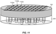
- FIG. 11 is a perspective view illustrating an embodiment of an inductor die after dicing of the joined SOC wafer and inductor wafer.
- multiple identical chips may be fabricated on a single wafer with a large surface area.
- a chip may be separated from a wafer by one of many dicing techniques known to persons skilled in the art.
- the joined SOC wafer 100 and the inductor wafer 200 may be diced into a plurality of dies 1102a, 1102b, 1102c, .... Any one of the dies 1102a, 1102b, 1102c, ... includes one or more inductors and one or more other components, such as one or more capacitors, as part of an integrated or embedded voltage regulator.
- FIG. 12 is a sectional view illustrating an embodiment of a system including a printed circuit board (PCB), an SOC package, and a voltage regulator which includes an inductor die.
- a printed circuit board (PCB) 1202 is provided, and an IC package 1204 is provided on the PCB 1202.
- the IC package may include one or more analog integrated circuits, one or more digital integrated circuits, or a combination thereof.
- the IC package 1204 may have one of various configurations known to persons skilled in the art, including but not limited to wirebond, flip-chip, or ball grid array (BGA), for example.
- BGA ball grid array
- a die 1206 that includes an inductor fabricated on an inductor wafer with through vias and joined with an SOC wafer in embodiments described above with respect to FIGs. 1-11 is integrated with the IC package 1204.
- the IC package 1204 includes a package substrate 1212.
- the die 1206 is provided as a part of the circuitry for an integrated or embedded voltage regulator 1208, which also includes other components.
- the voltage regulator 1208 may include one or more additional passive components such as one or more capacitors.
- the rest of the circuitry for the voltage regulator 1208 are generically indicated by block 1210.
- FIG. 13 is a simplified block diagram illustrating am embodiment of a system including a power management integrated circuit (PMIC) and an SOC device which includes an integrated or embedded voltage regulator and circuit using the voltage regulator.
- the PMIC 1302 is shown as a chip separate from the SOC device 1304. In an alternate embodiment, the PMIC 1302 may be integrated as part of the SOC device 1304.
- the SOC device includes an inductor and capacitor (L & C) block 1306, a voltage regulator (VR) 1308, and one or more circuits 1310 using the output voltage from the VR 1308.
- the inductor and capacitor in the L & C block 1306 may be integrated or embedded with the VR 1308 on the same chip as the circuits 1310 using the output voltage from the VR 1308 in an SOC device.
Landscapes
- Semiconductor Integrated Circuits (AREA)
- Engineering & Computer Science (AREA)
- Power Engineering (AREA)
- Physics & Mathematics (AREA)
- Geometry (AREA)
- Manufacturing & Machinery (AREA)
Applications Claiming Priority (2)
| Application Number | Priority Date | Filing Date | Title |
|---|---|---|---|
| US14/843,964 US20170062398A1 (en) | 2015-09-02 | 2015-09-02 | Integration of inductors with advanced-node system-on-chip (soc) using glass wafer with inductors and wafer-to-wafer joining |
| PCT/US2016/045998 WO2017039962A1 (en) | 2015-09-02 | 2016-08-08 | Integration of inductors with advanced-node system-on-chip (soc) using glass wafer with inductors and wafer-to-wafer joining |
Publications (3)
| Publication Number | Publication Date |
|---|---|
| EP3345218A1 EP3345218A1 (en) | 2018-07-11 |
| EP3345218B1 true EP3345218B1 (en) | 2025-06-25 |
| EP3345218C0 EP3345218C0 (en) | 2025-06-25 |
Family
ID=56684312
Family Applications (1)
| Application Number | Title | Priority Date | Filing Date |
|---|---|---|---|
| EP16751137.7A Active EP3345218B1 (en) | 2015-09-02 | 2016-08-08 | Integration of inductors with advanced-node system-on-chip (soc) using glass wafer with inductors and wafer-to-wafer joining |
Country Status (8)
| Country | Link |
|---|---|
| US (2) | US20170062398A1 (enExample) |
| EP (1) | EP3345218B1 (enExample) |
| JP (1) | JP2018532260A (enExample) |
| KR (1) | KR102541387B1 (enExample) |
| CN (1) | CN108012565A (enExample) |
| BR (1) | BR112018004288A2 (enExample) |
| CA (1) | CA2992855A1 (enExample) |
| WO (1) | WO2017039962A1 (enExample) |
Families Citing this family (7)
| Publication number | Priority date | Publication date | Assignee | Title |
|---|---|---|---|---|
| US9935076B1 (en) * | 2015-09-30 | 2018-04-03 | Apple Inc. | Structure and method for fabricating a computing system with an integrated voltage regulator module |
| US20170169934A1 (en) * | 2015-12-15 | 2017-06-15 | Globalfoundries Inc. | Patterned magnetic shields for inductors and transformers |
| US20200203067A1 (en) * | 2017-09-29 | 2020-06-25 | Intel Corporation | Magnetic core/shell particles for inductor arrays |
| US11538617B2 (en) | 2018-06-29 | 2022-12-27 | Intel Corporation | Integrated magnetic core inductors on glass core substrates |
| US11855124B2 (en) * | 2019-11-15 | 2023-12-26 | Qualcomm Incorporated | Vertically integrated device stack including system on chip and power management integrated circuit |
| US11450628B2 (en) * | 2019-12-15 | 2022-09-20 | Taiwan Semiconductor Manufacturing Company, Ltd. | Package structure including a solenoid inductor laterally aside a die and method of fabricating the same |
| KR102949699B1 (ko) | 2020-02-19 | 2026-04-10 | 삼성전자주식회사 | 반도체 패키지 |
Citations (3)
| Publication number | Priority date | Publication date | Assignee | Title |
|---|---|---|---|---|
| US20020095768A1 (en) * | 1999-07-09 | 2002-07-25 | Micron Technology, Inc. | Integrated circuit inductors |
| US7463131B1 (en) * | 2005-01-24 | 2008-12-09 | National Semiconductor Corporation | Patterned magnetic layer on-chip inductor |
| US20150137342A1 (en) * | 2013-11-20 | 2015-05-21 | Marvell World Trade Ltd. | Inductor/transformer outside of silicon wafer |
Family Cites Families (10)
| Publication number | Priority date | Publication date | Assignee | Title |
|---|---|---|---|---|
| US6531945B1 (en) * | 2000-03-10 | 2003-03-11 | Micron Technology, Inc. | Integrated circuit inductor with a magnetic core |
| US6992871B2 (en) * | 2003-08-06 | 2006-01-31 | Micron Technology, Inc. | Microtransformer for system-on-chip power supply |
| US20060088971A1 (en) * | 2004-10-27 | 2006-04-27 | Crawford Ankur M | Integrated inductor and method of fabrication |
| JP4929857B2 (ja) * | 2006-06-12 | 2012-05-09 | 株式会社日立製作所 | 半導体装置 |
| US9105627B2 (en) * | 2011-11-04 | 2015-08-11 | International Business Machines Corporation | Coil inductor for on-chip or on-chip stack |
| US10115671B2 (en) * | 2012-08-03 | 2018-10-30 | Snaptrack, Inc. | Incorporation of passives and fine pitch through via for package on package |
| US9041152B2 (en) * | 2013-03-14 | 2015-05-26 | Taiwan Semiconductor Manufacturing Company, Ltd. | Inductor with magnetic material |
| US9165791B2 (en) * | 2013-10-31 | 2015-10-20 | Qualcomm Incorporated | Wireless interconnects in an interposer |
| WO2015127207A1 (en) * | 2014-02-21 | 2015-08-27 | Marvell World Trade Ltd. | Method and apparatus for incorporating passive devices in an integrated passive device separate from a die |
| US9893141B2 (en) * | 2015-02-26 | 2018-02-13 | Taiwan Semiconductor Manufacturing Co., Ltd. | Magnetic core, inductor, and method for fabricating the magnetic core |
-
2015
- 2015-09-02 US US14/843,964 patent/US20170062398A1/en not_active Abandoned
-
2016
- 2016-08-08 EP EP16751137.7A patent/EP3345218B1/en active Active
- 2016-08-08 CA CA2992855A patent/CA2992855A1/en not_active Abandoned
- 2016-08-08 WO PCT/US2016/045998 patent/WO2017039962A1/en not_active Ceased
- 2016-08-08 KR KR1020187009210A patent/KR102541387B1/ko active Active
- 2016-08-08 CN CN201680048793.1A patent/CN108012565A/zh active Pending
- 2016-08-08 BR BR112018004288-9A patent/BR112018004288A2/en not_active Application Discontinuation
- 2016-08-08 JP JP2018509890A patent/JP2018532260A/ja active Pending
-
2021
- 2021-08-20 US US17/408,273 patent/US20210384292A1/en active Pending
Patent Citations (3)
| Publication number | Priority date | Publication date | Assignee | Title |
|---|---|---|---|---|
| US20020095768A1 (en) * | 1999-07-09 | 2002-07-25 | Micron Technology, Inc. | Integrated circuit inductors |
| US7463131B1 (en) * | 2005-01-24 | 2008-12-09 | National Semiconductor Corporation | Patterned magnetic layer on-chip inductor |
| US20150137342A1 (en) * | 2013-11-20 | 2015-05-21 | Marvell World Trade Ltd. | Inductor/transformer outside of silicon wafer |
Also Published As
| Publication number | Publication date |
|---|---|
| WO2017039962A1 (en) | 2017-03-09 |
| KR102541387B1 (ko) | 2023-06-08 |
| BR112018004288A2 (en) | 2018-10-09 |
| CA2992855A1 (en) | 2017-03-09 |
| KR20180048948A (ko) | 2018-05-10 |
| CN108012565A (zh) | 2018-05-08 |
| US20210384292A1 (en) | 2021-12-09 |
| JP2018532260A (ja) | 2018-11-01 |
| EP3345218C0 (en) | 2025-06-25 |
| US20170062398A1 (en) | 2017-03-02 |
| EP3345218A1 (en) | 2018-07-11 |
Similar Documents
| Publication | Publication Date | Title |
|---|---|---|
| EP3345218B1 (en) | Integration of inductors with advanced-node system-on-chip (soc) using glass wafer with inductors and wafer-to-wafer joining | |
| EP2754178B1 (en) | A small size and fully integrated power converter with magnetics on chip | |
| CN105185554B (zh) | 磁芯三维(3d)电感器及封装集成 | |
| CN101814485B (zh) | 具堆栈式电感和ic芯片的小型功率半导体封装及方法 | |
| TWI600037B (zh) | 無基板個別耦合電感器結構、電感器結構設備及用於提供電感器結構之方法 | |
| US9888577B2 (en) | Passive electrical devices with a polymer carrier | |
| JP6377178B2 (ja) | 埋込型パッケージ基板コンデンサ | |
| EP3257079A1 (en) | Switched power stage with integrated passive components | |
| US11723222B2 (en) | Integrated circuit (IC) package with integrated inductor having core magnetic field (B field) extending parallel to substrate | |
| KR20150119039A (ko) | 기판 내 커플링된 인덕터 구조 | |
| US10879169B2 (en) | Integrated inductors for power management circuits | |
| US11557420B2 (en) | Coupling inductors in an IC device using interconnecting elements with solder caps and resulting devices | |
| US10470309B2 (en) | Inductor and capacitor integrated on a substrate | |
| US9728507B2 (en) | Cap chip and reroute layer for stacked microelectronic module | |
| WO2009118694A1 (en) | Integrated 3d high density and high quality inductive element | |
| US20150311271A1 (en) | Landside embedded inductor for fanout packaging | |
| TWI862398B (zh) | 建構螺線管電感器的方法及以其建構的螺線管電感器 | |
| CN120569791A (zh) | 用于薄膜电感器的晶圆级封装工艺 |
Legal Events
| Date | Code | Title | Description |
|---|---|---|---|
| STAA | Information on the status of an ep patent application or granted ep patent |
Free format text: STATUS: THE INTERNATIONAL PUBLICATION HAS BEEN MADE |
|
| PUAI | Public reference made under article 153(3) epc to a published international application that has entered the european phase |
Free format text: ORIGINAL CODE: 0009012 |
|
| STAA | Information on the status of an ep patent application or granted ep patent |
Free format text: STATUS: REQUEST FOR EXAMINATION WAS MADE |
|
| 17P | Request for examination filed |
Effective date: 20180119 |
|
| AK | Designated contracting states |
Kind code of ref document: A1 Designated state(s): AL AT BE BG CH CY CZ DE DK EE ES FI FR GB GR HR HU IE IS IT LI LT LU LV MC MK MT NL NO PL PT RO RS SE SI SK SM TR |
|
| AX | Request for extension of the european patent |
Extension state: BA ME |
|
| DAV | Request for validation of the european patent (deleted) | ||
| DAX | Request for extension of the european patent (deleted) | ||
| STAA | Information on the status of an ep patent application or granted ep patent |
Free format text: STATUS: EXAMINATION IS IN PROGRESS |
|
| 17Q | First examination report despatched |
Effective date: 20210302 |
|
| GRAP | Despatch of communication of intention to grant a patent |
Free format text: ORIGINAL CODE: EPIDOSNIGR1 |
|
| STAA | Information on the status of an ep patent application or granted ep patent |
Free format text: STATUS: GRANT OF PATENT IS INTENDED |
|
| RIC1 | Information provided on ipc code assigned before grant |
Ipc: H01L 23/498 20060101ALI20250108BHEP Ipc: H01L 23/64 20060101AFI20250108BHEP |
|
| INTG | Intention to grant announced |
Effective date: 20250121 |
|
| GRAS | Grant fee paid |
Free format text: ORIGINAL CODE: EPIDOSNIGR3 |
|
| GRAA | (expected) grant |
Free format text: ORIGINAL CODE: 0009210 |
|
| STAA | Information on the status of an ep patent application or granted ep patent |
Free format text: STATUS: THE PATENT HAS BEEN GRANTED |
|
| AK | Designated contracting states |
Kind code of ref document: B1 Designated state(s): AL AT BE BG CH CY CZ DE DK EE ES FI FR GB GR HR HU IE IS IT LI LT LU LV MC MK MT NL NO PL PT RO RS SE SI SK SM TR |
|
| REG | Reference to a national code |
Ref country code: GB Ref legal event code: FG4D |
|
| REG | Reference to a national code |
Ref country code: CH Ref legal event code: EP |
|
| REG | Reference to a national code |
Ref country code: CH Ref legal event code: EP |
|
| REG | Reference to a national code |
Ref country code: IE Ref legal event code: FG4D |
|
| REG | Reference to a national code |
Ref country code: DE Ref legal event code: R096 Ref document number: 602016092659 Country of ref document: DE |
|
| U01 | Request for unitary effect filed |
Effective date: 20250709 |
|
| U07 | Unitary effect registered |
Designated state(s): AT BE BG DE DK EE FI FR IT LT LU LV MT NL PT RO SE SI Effective date: 20250716 |
|
| U20 | Renewal fee for the european patent with unitary effect paid |
Year of fee payment: 10 Effective date: 20250724 |
|
| PG25 | Lapsed in a contracting state [announced via postgrant information from national office to epo] |
Ref country code: GR Free format text: LAPSE BECAUSE OF FAILURE TO SUBMIT A TRANSLATION OF THE DESCRIPTION OR TO PAY THE FEE WITHIN THE PRESCRIBED TIME-LIMIT Effective date: 20250926 Ref country code: NO Free format text: LAPSE BECAUSE OF FAILURE TO SUBMIT A TRANSLATION OF THE DESCRIPTION OR TO PAY THE FEE WITHIN THE PRESCRIBED TIME-LIMIT Effective date: 20250925 |
|
| PGFP | Annual fee paid to national office [announced via postgrant information from national office to epo] |
Ref country code: GB Payment date: 20250814 Year of fee payment: 10 |
|
| PG25 | Lapsed in a contracting state [announced via postgrant information from national office to epo] |
Ref country code: HR Free format text: LAPSE BECAUSE OF FAILURE TO SUBMIT A TRANSLATION OF THE DESCRIPTION OR TO PAY THE FEE WITHIN THE PRESCRIBED TIME-LIMIT Effective date: 20250625 |
|
| PG25 | Lapsed in a contracting state [announced via postgrant information from national office to epo] |
Ref country code: RS Free format text: LAPSE BECAUSE OF FAILURE TO SUBMIT A TRANSLATION OF THE DESCRIPTION OR TO PAY THE FEE WITHIN THE PRESCRIBED TIME-LIMIT Effective date: 20250925 |
|
| PGFP | Annual fee paid to national office [announced via postgrant information from national office to epo] |
Ref country code: IE Payment date: 20250808 Year of fee payment: 10 |
|
| PG25 | Lapsed in a contracting state [announced via postgrant information from national office to epo] |
Ref country code: IS Free format text: LAPSE BECAUSE OF FAILURE TO SUBMIT A TRANSLATION OF THE DESCRIPTION OR TO PAY THE FEE WITHIN THE PRESCRIBED TIME-LIMIT Effective date: 20251025 |
|
| PG25 | Lapsed in a contracting state [announced via postgrant information from national office to epo] |
Ref country code: SM Free format text: LAPSE BECAUSE OF FAILURE TO SUBMIT A TRANSLATION OF THE DESCRIPTION OR TO PAY THE FEE WITHIN THE PRESCRIBED TIME-LIMIT Effective date: 20250625 |
|
| PG25 | Lapsed in a contracting state [announced via postgrant information from national office to epo] |
Ref country code: CZ Free format text: LAPSE BECAUSE OF FAILURE TO SUBMIT A TRANSLATION OF THE DESCRIPTION OR TO PAY THE FEE WITHIN THE PRESCRIBED TIME-LIMIT Effective date: 20250625 |
|
| PG25 | Lapsed in a contracting state [announced via postgrant information from national office to epo] |
Ref country code: PL Free format text: LAPSE BECAUSE OF FAILURE TO SUBMIT A TRANSLATION OF THE DESCRIPTION OR TO PAY THE FEE WITHIN THE PRESCRIBED TIME-LIMIT Effective date: 20250625 |
|
| PG25 | Lapsed in a contracting state [announced via postgrant information from national office to epo] |
Ref country code: SK Free format text: LAPSE BECAUSE OF FAILURE TO SUBMIT A TRANSLATION OF THE DESCRIPTION OR TO PAY THE FEE WITHIN THE PRESCRIBED TIME-LIMIT Effective date: 20250625 |
|
| PG25 | Lapsed in a contracting state [announced via postgrant information from national office to epo] |
Ref country code: ES Free format text: LAPSE BECAUSE OF FAILURE TO SUBMIT A TRANSLATION OF THE DESCRIPTION OR TO PAY THE FEE WITHIN THE PRESCRIBED TIME-LIMIT Effective date: 20250625 |
|
| REG | Reference to a national code |
Ref country code: CH Ref legal event code: H13 Free format text: ST27 STATUS EVENT CODE: U-0-0-H10-H13 (AS PROVIDED BY THE NATIONAL OFFICE) Effective date: 20260324 |
|
| PG25 | Lapsed in a contracting state [announced via postgrant information from national office to epo] |
Ref country code: MC Free format text: LAPSE BECAUSE OF FAILURE TO SUBMIT A TRANSLATION OF THE DESCRIPTION OR TO PAY THE FEE WITHIN THE PRESCRIBED TIME-LIMIT Effective date: 20250625 |
|
| PG25 | Lapsed in a contracting state [announced via postgrant information from national office to epo] |
Ref country code: CH Free format text: LAPSE BECAUSE OF NON-PAYMENT OF DUE FEES Effective date: 20250831 |
|
| PLBE | No opposition filed within time limit |
Free format text: ORIGINAL CODE: 0009261 |
|
| STAA | Information on the status of an ep patent application or granted ep patent |
Free format text: STATUS: NO OPPOSITION FILED WITHIN TIME LIMIT |