EP3328039B1 - Anzeigevorrichtung mit einem fingerabdrucksensor - Google Patents
Anzeigevorrichtung mit einem fingerabdrucksensor Download PDFInfo
- Publication number
- EP3328039B1 EP3328039B1 EP17202959.7A EP17202959A EP3328039B1 EP 3328039 B1 EP3328039 B1 EP 3328039B1 EP 17202959 A EP17202959 A EP 17202959A EP 3328039 B1 EP3328039 B1 EP 3328039B1
- Authority
- EP
- European Patent Office
- Prior art keywords
- fingerprint sensor
- light
- display panel
- display device
- transparent substrate
- Prior art date
- Legal status (The legal status is an assumption and is not a legal conclusion. Google has not performed a legal analysis and makes no representation as to the accuracy of the status listed.)
- Active
Links
Images





Classifications
-
- G—PHYSICS
- G06—COMPUTING OR CALCULATING; COUNTING
- G06F—ELECTRIC DIGITAL DATA PROCESSING
- G06F1/00—Details not covered by groups G06F3/00 - G06F13/00 and G06F21/00
- G06F1/16—Constructional details or arrangements
- G06F1/1613—Constructional details or arrangements for portable computers
- G06F1/1626—Constructional details or arrangements for portable computers with a single-body enclosure integrating a flat display, e.g. Personal Digital Assistants [PDAs]
-
- G—PHYSICS
- G09—EDUCATION; CRYPTOGRAPHY; DISPLAY; ADVERTISING; SEALS
- G09F—DISPLAYING; ADVERTISING; SIGNS; LABELS OR NAME-PLATES; SEALS
- G09F9/00—Indicating arrangements for variable information in which the information is built-up on a support by selection or combination of individual elements
-
- G—PHYSICS
- G06—COMPUTING OR CALCULATING; COUNTING
- G06F—ELECTRIC DIGITAL DATA PROCESSING
- G06F1/00—Details not covered by groups G06F3/00 - G06F13/00 and G06F21/00
- G06F1/16—Constructional details or arrangements
- G06F1/1613—Constructional details or arrangements for portable computers
- G06F1/1633—Constructional details or arrangements of portable computers not specific to the type of enclosures covered by groups G06F1/1615 - G06F1/1626
- G06F1/1637—Details related to the display arrangement, including those related to the mounting of the display in the housing
- G06F1/1643—Details related to the display arrangement, including those related to the mounting of the display in the housing the display being associated to a digitizer, e.g. laptops that can be used as penpads
-
- G—PHYSICS
- G06—COMPUTING OR CALCULATING; COUNTING
- G06F—ELECTRIC DIGITAL DATA PROCESSING
- G06F1/00—Details not covered by groups G06F3/00 - G06F13/00 and G06F21/00
- G06F1/16—Constructional details or arrangements
- G06F1/1613—Constructional details or arrangements for portable computers
- G06F1/1633—Constructional details or arrangements of portable computers not specific to the type of enclosures covered by groups G06F1/1615 - G06F1/1626
- G06F1/1684—Constructional details or arrangements related to integrated I/O peripherals not covered by groups G06F1/1635 - G06F1/1675
-
- G—PHYSICS
- G06—COMPUTING OR CALCULATING; COUNTING
- G06V—IMAGE OR VIDEO RECOGNITION OR UNDERSTANDING
- G06V40/00—Recognition of biometric, human-related or animal-related patterns in image or video data
- G06V40/10—Human or animal bodies, e.g. vehicle occupants or pedestrians; Body parts, e.g. hands
- G06V40/12—Fingerprints or palmprints
- G06V40/13—Sensors therefor
-
- G—PHYSICS
- G06—COMPUTING OR CALCULATING; COUNTING
- G06V—IMAGE OR VIDEO RECOGNITION OR UNDERSTANDING
- G06V40/00—Recognition of biometric, human-related or animal-related patterns in image or video data
- G06V40/10—Human or animal bodies, e.g. vehicle occupants or pedestrians; Body parts, e.g. hands
- G06V40/12—Fingerprints or palmprints
- G06V40/13—Sensors therefor
- G06V40/1306—Sensors therefor non-optical, e.g. ultrasonic or capacitive sensing
-
- G—PHYSICS
- G06—COMPUTING OR CALCULATING; COUNTING
- G06V—IMAGE OR VIDEO RECOGNITION OR UNDERSTANDING
- G06V40/00—Recognition of biometric, human-related or animal-related patterns in image or video data
- G06V40/10—Human or animal bodies, e.g. vehicle occupants or pedestrians; Body parts, e.g. hands
- G06V40/12—Fingerprints or palmprints
- G06V40/13—Sensors therefor
- G06V40/1318—Sensors therefor using electro-optical elements or layers, e.g. electroluminescent sensing
-
- H—ELECTRICITY
- H04—ELECTRIC COMMUNICATION TECHNIQUE
- H04M—TELEPHONIC COMMUNICATION
- H04M1/00—Substation equipment, e.g. for use by subscribers
- H04M1/02—Constructional features of telephone sets
- H04M1/0202—Portable telephone sets, e.g. cordless phones, mobile phones or bar type handsets
- H04M1/026—Details of the structure or mounting of specific components
- H04M1/0266—Details of the structure or mounting of specific components for a display module assembly
-
- H—ELECTRICITY
- H10—SEMICONDUCTOR DEVICES; ELECTRIC SOLID-STATE DEVICES NOT OTHERWISE PROVIDED FOR
- H10K—ORGANIC ELECTRIC SOLID-STATE DEVICES
- H10K50/00—Organic light-emitting devices
- H10K50/80—Constructional details
- H10K50/84—Passivation; Containers; Encapsulations
-
- H—ELECTRICITY
- H10—SEMICONDUCTOR DEVICES; ELECTRIC SOLID-STATE DEVICES NOT OTHERWISE PROVIDED FOR
- H10K—ORGANIC ELECTRIC SOLID-STATE DEVICES
- H10K50/00—Organic light-emitting devices
- H10K50/80—Constructional details
- H10K50/86—Arrangements for improving contrast, e.g. preventing reflection of ambient light
-
- H—ELECTRICITY
- H10—SEMICONDUCTOR DEVICES; ELECTRIC SOLID-STATE DEVICES NOT OTHERWISE PROVIDED FOR
- H10K—ORGANIC ELECTRIC SOLID-STATE DEVICES
- H10K59/00—Integrated devices, or assemblies of multiple devices, comprising at least one organic light-emitting element covered by group H10K50/00
- H10K59/40—OLEDs integrated with touch screens
-
- H—ELECTRICITY
- H10—SEMICONDUCTOR DEVICES; ELECTRIC SOLID-STATE DEVICES NOT OTHERWISE PROVIDED FOR
- H10K—ORGANIC ELECTRIC SOLID-STATE DEVICES
- H10K77/00—Constructional details of devices covered by this subclass and not covered by groups H10K10/80, H10K30/80, H10K50/80 or H10K59/80
- H10K77/10—Substrates, e.g. flexible substrates
- H10K77/111—Flexible substrates
-
- H—ELECTRICITY
- H04—ELECTRIC COMMUNICATION TECHNIQUE
- H04M—TELEPHONIC COMMUNICATION
- H04M1/00—Substation equipment, e.g. for use by subscribers
- H04M1/02—Constructional features of telephone sets
- H04M1/0202—Portable telephone sets, e.g. cordless phones, mobile phones or bar type handsets
- H04M1/026—Details of the structure or mounting of specific components
-
- H—ELECTRICITY
- H04—ELECTRIC COMMUNICATION TECHNIQUE
- H04M—TELEPHONIC COMMUNICATION
- H04M1/00—Substation equipment, e.g. for use by subscribers
- H04M1/66—Substation equipment, e.g. for use by subscribers with means for preventing unauthorised or fraudulent calling
- H04M1/667—Preventing unauthorised calls from a telephone set
- H04M1/67—Preventing unauthorised calls from a telephone set by electronic means
-
- H—ELECTRICITY
- H10—SEMICONDUCTOR DEVICES; ELECTRIC SOLID-STATE DEVICES NOT OTHERWISE PROVIDED FOR
- H10K—ORGANIC ELECTRIC SOLID-STATE DEVICES
- H10K2102/00—Constructional details relating to the organic devices covered by this subclass
- H10K2102/301—Details of OLEDs
- H10K2102/311—Flexible OLED
-
- H—ELECTRICITY
- H10—SEMICONDUCTOR DEVICES; ELECTRIC SOLID-STATE DEVICES NOT OTHERWISE PROVIDED FOR
- H10K—ORGANIC ELECTRIC SOLID-STATE DEVICES
- H10K59/00—Integrated devices, or assemblies of multiple devices, comprising at least one organic light-emitting element covered by group H10K50/00
- H10K59/60—OLEDs integrated with inorganic light-sensitive elements, e.g. with inorganic solar cells or inorganic photodiodes
- H10K59/65—OLEDs integrated with inorganic image sensors
-
- H—ELECTRICITY
- H10—SEMICONDUCTOR DEVICES; ELECTRIC SOLID-STATE DEVICES NOT OTHERWISE PROVIDED FOR
- H10K—ORGANIC ELECTRIC SOLID-STATE DEVICES
- H10K59/00—Integrated devices, or assemblies of multiple devices, comprising at least one organic light-emitting element covered by group H10K50/00
- H10K59/80—Constructional details
- H10K59/87—Passivation; Containers; Encapsulations
- H10K59/871—Self-supporting sealing arrangements
- H10K59/8722—Peripheral sealing arrangements, e.g. adhesives, sealants
-
- H—ELECTRICITY
- H10—SEMICONDUCTOR DEVICES; ELECTRIC SOLID-STATE DEVICES NOT OTHERWISE PROVIDED FOR
- H10K—ORGANIC ELECTRIC SOLID-STATE DEVICES
- H10K59/00—Integrated devices, or assemblies of multiple devices, comprising at least one organic light-emitting element covered by group H10K50/00
- H10K59/80—Constructional details
- H10K59/8791—Arrangements for improving contrast, e.g. preventing reflection of ambient light
-
- Y—GENERAL TAGGING OF NEW TECHNOLOGICAL DEVELOPMENTS; GENERAL TAGGING OF CROSS-SECTIONAL TECHNOLOGIES SPANNING OVER SEVERAL SECTIONS OF THE IPC; TECHNICAL SUBJECTS COVERED BY FORMER USPC CROSS-REFERENCE ART COLLECTIONS [XRACs] AND DIGESTS
- Y02—TECHNOLOGIES OR APPLICATIONS FOR MITIGATION OR ADAPTATION AGAINST CLIMATE CHANGE
- Y02E—REDUCTION OF GREENHOUSE GAS [GHG] EMISSIONS, RELATED TO ENERGY GENERATION, TRANSMISSION OR DISTRIBUTION
- Y02E10/00—Energy generation through renewable energy sources
- Y02E10/50—Photovoltaic [PV] energy
- Y02E10/549—Organic PV cells
Definitions
- the fingerprint sensor module 23 does not need to be connected to the drive IC 25.
- the first flexible substrate 24 where the fingerprint sensor module 23 is mounted may be connected to the host system's mainboard without via holes like in FIG. 10 .
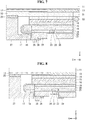
- FIG. 9 is a cross-sectional view of a display device according to an eighth example embodiment of the present invention.
- Components substantially identical to those in the foregoing example embodiments are denoted by the same reference numerals, and detailed descriptions of them will be omitted, or may be briefly discussed.
- An incident beam 100 of collimated light from the light source LS has a given cross-sectional area and is provided to an incident point IP defined on the light-entering element CHOE. It is desirable that the incident beam 100 enters in a direction normal to the surface of the incident point IP. However, the present invention is not limited to this, and if necessary, the incident beam 100 may enter at an oblique angle from the direction normal to the surface of the incident point IP.
- the outgoing beam 300 is emitted gradually by the light-exiting element VHOE as it travels from the light-entering element CHOE.
- the amount of light in the outgoing beam 300 is determined by the light extraction efficiency of the light-exiting element VHOE. For example, if the light extraction efficiency of the light-exiting element VHOE is 3 %, 3 % of the initial incident beam 100 is extracted as the outgoing beam 300, in a first light-emission region where the traveling beam 200 first touches the light-exiting element VHOE, while 97% of the initial incident beam as the traveling beam 200 continues to be totally reflected and travel. Afterwards, in a second light-emission region, 2.91 % of the initial incident beam 100, which equals 3 % of the remaining 97 %, is extracted as the outgoing beam 300.
- the region where the light-entering element CHOE is situated may be defined as a light input portion LIN.
- the region where the light-exiting element VHOE is situated may be defined as the light output portion LOT.
- the light output portion LOT may be a light travel portion along which light travels.
- the light-entering element CHOE may have a length corresponding to the width of the transparent substrate CP and a width of around 3 mm to 5 mm.
- the light-entering element CHOE may be situated across the width of the transparent substrate CP.
- the traveling beam 200 is totally reflected off the upper surface of the transparent substrate CP since the upper surface of the transparent substrate CP is in contact with an air layer AIR.
- the total reflection critical angle TCP_AIR at the interface between the transparent substrate CP and the air layer AIR is around 41.4 degrees. That is, as long as the incident angle ( ⁇ ) is greater than the total reflection critical angle TVHOE_LR at the interface between the light-exiting element VHOE and the low refractive index layer LR, the incident angle ( ⁇ ) is always greater than the total reflection critical angle TCP_AIR at the interface between the transparent substrate CP and the air layer AIR.
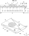
- a display device comprises a directional light source device SLS and a display panel DP situated under the directional light source device SLS, as shown in FIG. 14 .
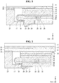
- a display device may be implemented in the structures shown in FIGS. 2 , 5 , 7 , and 9 .
- an incident beam 100 is converted into a traveling beam 200 by the light-entering element CHOE.
- the traveling beam 200 is converted in such a way that it has a spread angle ( ⁇ ) on the XY plane, which is a horizontal plane consisting of an X-axis along the length and a Y-axis along the width.
- ⁇ spread angle
- the traveling beam 200 remains collimated, as it originally was, on the XZ plane, which is a vertical plane consisting of an X-axis along the length and a Y-axis along the thickness.
- the sensing area SA is formed at the center of the display panel DP or at a part of the upper edge of the display panel DP, opposite the light-entering element CHOE, it is desirable that the amount of light in the outgoing beam 300 is largest in the sensing area SA.
- the light extraction efficiency of the light-exiting element VHOE may be designed as a function of position so that it is highest in the part corresponding to the sensing area SA and lowest or close to zero in the other parts.
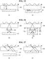
- FIG. 15 is a view of an ultrasonic wave path which varies depending on the presence or absence of an air layer between a medium and an ultrasonic fingerprint sensor.
- the medium 150 in FIG. 15 is a medium that comprises a transparent substrate, a light-exiting element, a low refractive index layer, and a display panel. If there is no air layer 152 in the medium 150, as shown in (A) of FIG. 15 , an ultrasonic wave may pass through the medium 150 and be reflected off a fingerprint IM and received by the receiving portion of the ultrasonic fingerprint sensor. On the other hand, if there is an air layer 152 between the ultrasonic fingerprint sensor and the medium 150, as shown in (B) of FIG. 15 , an ultrasonic wave from the ultrasonic fingerprint sensor does not reach as far as the fingerprint IM but is reflected off the surface of the medium 150 and therefore cannot sense a fingerprint pattern.
- the light reception efficiency of the optical fingerprint sensor 23 is low if there is an air layer between the optical fingerprint sensor 23 and the medium 150, which reduces sensing performance.
- a lens 23a is placed in front of the receiving portion of the optical fingerprint sensor 23, as shown in (A) of FIG. 16 , light is collimated by the lens 23a and directed onto the receiving portion, and therefore fingerprint sensing is possible even if there is an air layer in front of the receiving portion.
- the lens 23a may be situated opposite the receiving portion 23b within a space provided by a cylindrical sidewall 23c in the optical fingerprint sensor 23. The top of the sidewall 23a is bonded to the display panel with an adhesive 22.
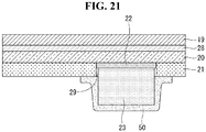
- the non-transparent film 50 is bonded onto the metallic layer 21 and the fingerprint sensor 23 so as to cover the fingerprint sensor 23 and the gap 29 around it.
- the non-transparent film 50 may be a black or dark-colored adhesive film or resin.
- the adhesive 22 for bonding the fingerprint sensor 23 onto the back plate 19 may be a transparent adhesive or an opaque adhesive.
- the opaque adhesive may be a colored adhesive.
- An example of the transparent adhesive may be transparent OCR, and an example of the colored adhesive may be a dark-colored or black OCR, but the present invention is not limited to them.
- the non-transparent film 50 may be omitted as shown in FIG. 19 because the opaque adhesive can substitute for the non-transparent film 50.
- the foam pad 20 may be bonded to the back plate 19 with an adhesive 28 such as OCA.
- the fingerprint sensor 23 may be bonded to the back plate 19 using the same adhesive 28 as the foam pad 20, as shown in FIG. 20 , rather than using a separate adhesive 22.
- a UV pass filter for blocking light of visible wavelengths and passing UV light may be mixed in with the adhesives 22 and 28 opposite the receiving portion of the fingerprint sensor 23. In this case, there is no need to add a separate UV pass filter to the optical fingerprint sensor.
- a display device can detect a fingerprint on a screen, without increasing bezel size or altering display panel structure, by placing a fingerprint sensor module under a pixel array with light-emitting diodes and bonding the fingerprint sensor module to the display panel.
- the present invention can secure a path of ultrasonic waves or light between a transparent substrate where a fingerprint touches and the fingerprint sensor module by forming a hole in a metallic layer for blocking electromagnetic interference EMI and inserting the fingerprint sensor module in the hole.
Landscapes
- Engineering & Computer Science (AREA)
- Theoretical Computer Science (AREA)
- Physics & Mathematics (AREA)
- General Physics & Mathematics (AREA)
- Human Computer Interaction (AREA)
- Computer Hardware Design (AREA)
- Multimedia (AREA)
- General Engineering & Computer Science (AREA)
- Signal Processing (AREA)
- Optics & Photonics (AREA)
- Image Input (AREA)
- Devices For Indicating Variable Information By Combining Individual Elements (AREA)
- Measurement Of The Respiration, Hearing Ability, Form, And Blood Characteristics Of Living Organisms (AREA)
Claims (14)
- Anzeigevorrichtung, die Folgendes umfasst:ein Anzeigefeld (14, 15, 16, 17, 19), das konfiguriert ist, ein Bild auf einer Anzeigefläche anzuzeigen;ein transparentes Substrat (11), das auf dem Anzeigefeld (14, 15, 16, 17, 19) angeordnet ist, wobei die Anzeigefläche des Anzeigefelds (14, 15, 16, 17, 19) dem transparenten Substrat (11) zugewandt ist;einen Fingerabdrucksensor (23), der konfiguriert ist, einen Fingerabdruck zu detektieren, der das transparente Substrat (11) berührt, wobei das Anzeigefeld (14, 15, 16, 17, 19) zwischen dem Fingerabdrucksensor (23) und dem transparenten Substrat (11) angeordnet ist;eine integrierte Steuerschaltung (25), Steuer-IC (25), die konfiguriert ist, das Anzeigefeld (14, 15, 16, 17, 19) zu steuern;ein Schaumpolster (20), das auf einer Oberfläche des Anzeigefelds (14, 15, 16, 17, 19) angeordnet ist, das von dem transparenten Substrat (11) abgewandt ist; undeine Metallschicht (21), wobei das Schaumpolster (20) zwischen der Metallschicht (21) und der Oberfläche des Anzeigefelds (14, 15, 16, 17, 19) angeordnet ist.
- Anzeigevorrichtung nach Anspruch 1,
wobei die Metallschicht (21) ein Loch umfasst, das das Schaumpolster (20) freilegt, und der Fingerabdrucksensor (23) in dem Loch mit einer Oberfläche des Schaumpolsters (20) verbunden ist. - Anzeigevorrichtung nach Anspruch 1,
wobei das Schaumpolster (20) und die Metallschicht (21) ein Loch (30) aufweisen, das das Anzeigefeld (14, 15, 16, 17, 19) freilegt, und der Fingerabdrucksensor (23) in dem Loch (30) mit einer Oberfläche des Anzeigefelds (14, 15, 16, 17, 19) verbunden ist. - Anzeigevorrichtung nach Anspruch 2 oder 3, die ferner einen nicht transparenten Film umfasst, der auf der Metallschicht (21) angeordnet ist und das Loch (30) und den Fingerabdrucksensor (23) bedeckt.
- Anzeigevorrichtung nach einem der vorhergehenden Ansprüche, die ferner Folgendes umfasst:ein Lichteintrittselement (31);ein Lichtaustrittselement (32), das neben dem Lichteintrittselement (31) und zwischen dem Anzeigefeld (14, 15, 16, 17, 19) und dem transparenten Substrat (11) in der Anzeigefläche angeordnet ist; undeine Lichtquelle (33) neben dem Lichteintrittselement (31) zum Emittieren von Licht auf das Lichteintrittselement (31).
- Anzeigevorrichtung nach Anspruch 5, wobei das Lichteintrittselement (31) und/oder das Lichtaustrittselement (32) ein holographisches Muster umfassen.
- Anzeigevorrichtung nach einem der vorhergehenden Ansprüche, wobei das Anzeigefeld (14, 15, 16, 17, 19) Folgendes umfasst:eine Rückplatte (19);eine organische Dünnschicht (17) auf der Rückplatte (19);eine Pixel-Anordnung (16) auf der organische Dünnschicht (17);eine Berührungssensor-Anordnung (15) auf der Pixel-Anordnung (16);einen Polarisationsfilm (14) auf der Berührungssensor-Anordnung (15).
- Anzeigevorrichtung nach Anspruch 7, die ferner Folgendes umfasst:ein erstes flexibles Substrat (24), auf dem der Fingerabdrucksensor (23) angeordnet ist; undein zweites flexibles Substrat (26), auf dem die Steuer-IC (25) angeordnet ist.
- Anzeigevorrichtung nach Anspruch 8, wobei das erste flexible Substrat (24) und das zweite flexible Substrat (26) gedruckte Schaltplatten enthalten und miteinander verbunden sind.
- Anzeigevorrichtung nach Anspruch 8 oder 9, die ferner einen Spanndorn (18) umfasst, wobei ein Abschnitt der organischen Dünnschicht (17) gekrümmt ist und mit dem zweiten flexiblen Substrat verbunden ist, und der Spanndorn (18) den gekrümmten Abschnitt der organischen Dünnschicht (17) trägt.
- Anzeigevorrichtung nach einem der vorhergehenden Ansprüche, die ferner eine Linse (23a) umfasst, die vor einem Aufnahmeabschnitt (23b) des Fingerabdrucksensors (23) positioniert ist.
- Anzeigevorrichtung nach einem der vorhergehenden Ansprüche, die ferner einen Rahmen (27) umfasst, der das Anzeigefeld (14, 15, 16, 17, 19), den Fingerabdrucksensor (23) und die Steuer-IC (25) aufnimmt, und eine Seitenwand aufweist, die mit dem transparenten Substrat (11) verbunden ist.
- Anzeigevorrichtung nach einem der vorhergehenden Ansprüche, wobei der Fingerabdrucksensor (23) mit einer Oberfläche des Anzeigefelds (14, 15, 16, 17, 19) durch ein nicht transparentes Klebemittel (22) verbunden ist.
- Anzeigevorrichtung nach einem der vorhergehenden Ansprüche, wobei der Fingerabdrucksensor (23) einen Ultraschall-Fingerabdrucksensor und/oder einen optischen Fingerabdrucksensor umfasst.
Applications Claiming Priority (2)
| Application Number | Priority Date | Filing Date | Title |
|---|---|---|---|
| KR20160158471 | 2016-11-25 | ||
| KR1020170053800A KR102483072B1 (ko) | 2016-11-25 | 2017-04-26 | 표시장치 |
Publications (2)
| Publication Number | Publication Date |
|---|---|
| EP3328039A1 EP3328039A1 (de) | 2018-05-30 |
| EP3328039B1 true EP3328039B1 (de) | 2021-06-16 |
Family
ID=60450457
Family Applications (1)
| Application Number | Title | Priority Date | Filing Date |
|---|---|---|---|
| EP17202959.7A Active EP3328039B1 (de) | 2016-11-25 | 2017-11-22 | Anzeigevorrichtung mit einem fingerabdrucksensor |
Country Status (4)
| Country | Link |
|---|---|
| US (1) | US10741621B2 (de) |
| EP (1) | EP3328039B1 (de) |
| JP (1) | JP6698617B2 (de) |
| CN (1) | CN108109523B (de) |
Families Citing this family (88)
| Publication number | Priority date | Publication date | Assignee | Title |
|---|---|---|---|---|
| US9710689B2 (en) * | 2015-10-30 | 2017-07-18 | Essential Products, Inc. | Fingerprint sensors for mobile devices |
| KR102481643B1 (ko) * | 2017-01-31 | 2022-12-28 | 삼성전자주식회사 | 디스플레이 제어 방법 및 전자 장치 |
| KR102752942B1 (ko) * | 2017-02-24 | 2025-01-10 | 삼성전자 주식회사 | 디스플레이에 통합된 생체 센서를 포함하는 전자장치 |
| CN107133613B (zh) * | 2017-06-06 | 2020-06-30 | 上海天马微电子有限公司 | 一种显示面板及显示装置 |
| TWI614695B (zh) * | 2017-07-03 | 2018-02-11 | 敦泰電子有限公司 | 具指紋辨識之高屏佔比顯示裝置 |
| TWI666753B (zh) * | 2017-09-28 | 2019-07-21 | 致伸科技股份有限公司 | 光學指紋感測單元及其製造方法 |
| KR102111045B1 (ko) * | 2017-10-31 | 2020-05-14 | 엘지디스플레이 주식회사 | 표시장치 |
| CN107818733B (zh) * | 2017-11-22 | 2020-02-11 | Oppo广东移动通信有限公司 | 显示屏组件及电子设备 |
| CN108242462B (zh) * | 2018-01-12 | 2020-08-18 | 京东方科技集团股份有限公司 | 有机发光显示面板及其制备方法、显示装置 |
| KR102443229B1 (ko) * | 2018-01-23 | 2022-09-15 | 삼성전자주식회사 | 센서를 장착하기 위한 개구를 포함하는 디스플레이 |
| JP6770082B2 (ja) * | 2018-02-06 | 2020-10-14 | シェンチェン グディックス テクノロジー カンパニー,リミテッド | アンダースクリーンバイオメトリクス認証装置、バイオメトリクス認証ユニット及び端末装置 |
| KR102504122B1 (ko) * | 2018-03-05 | 2023-02-28 | 삼성디스플레이 주식회사 | 표시 장치 |
| KR102445512B1 (ko) * | 2018-03-30 | 2022-09-21 | 삼성디스플레이 주식회사 | 지문 센서 패키지 및 이를 포함하는 표시 장치 |
| EP3940504B1 (de) * | 2018-04-17 | 2024-08-28 | Samsung Electronics Co., Ltd. | Elektronische vorrichtung mit mehreren befestigungselementen zur befestigung eines biometrischen sensors an der anzeige und verfahren zur herstellung davon |
| KR102658176B1 (ko) * | 2018-04-24 | 2024-04-18 | 삼성디스플레이 주식회사 | 표시장치 |
| KR102623375B1 (ko) * | 2018-06-08 | 2024-01-11 | 삼성디스플레이 주식회사 | 표시장치 및 이의 제조 방법 |
| KR20200002048A (ko) * | 2018-06-28 | 2020-01-08 | 삼성디스플레이 주식회사 | 전자 장치 |
| EP3796213A4 (de) * | 2018-07-17 | 2021-08-04 | Lg Chem, Ltd. | Optisches fingerabdruckerkennungssystem und mobile vorrichtung damit |
| CN110739327B (zh) * | 2018-07-20 | 2022-06-07 | 京东方科技集团股份有限公司 | 阵列基板及其制造方法、显示装置 |
| KR102576868B1 (ko) * | 2018-07-31 | 2023-09-11 | 삼성디스플레이 주식회사 | 표시장치 |
| KR102500131B1 (ko) * | 2018-08-06 | 2023-02-15 | 삼성전자주식회사 | 디스플레이의 후면에 배치된 센서 및 탄성 부재 사이의 높이 차를 보상하는 구조를 포함하는 전자 장치 |
| CN109240550B (zh) * | 2018-08-10 | 2022-04-15 | 业泓科技(成都)有限公司 | 触控显示模组以及应用该触控显示模组的电子装置 |
| KR102555513B1 (ko) * | 2018-08-17 | 2023-07-17 | 삼성디스플레이 주식회사 | 전자 장치 |
| WO2020034184A1 (zh) * | 2018-08-17 | 2020-02-20 | 上海箩箕技术有限公司 | 光学指纹传感器装置及其组装方法 |
| KR102495667B1 (ko) * | 2018-08-23 | 2023-02-03 | 삼성전자주식회사 | 디스플레이의 아래에 배치된 센서를 포함하는 전자 장치 |
| CN109244108B (zh) * | 2018-08-29 | 2020-11-03 | 京东方科技集团股份有限公司 | 一种oled显示基板及其制作方法、oled显示装置 |
| KR102555954B1 (ko) * | 2018-08-31 | 2023-07-19 | 삼성디스플레이 주식회사 | 표시 장치 |
| KR102689899B1 (ko) * | 2018-09-07 | 2024-07-29 | 삼성디스플레이 주식회사 | 표시 장치 |
| CN109166469B (zh) * | 2018-09-14 | 2021-03-02 | 京东方科技集团股份有限公司 | 显示面板及制作方法、显示装置 |
| KR102582465B1 (ko) | 2018-09-19 | 2023-09-25 | 삼성디스플레이 주식회사 | 표시 장치 |
| CN114299827B (zh) * | 2018-10-11 | 2023-11-17 | 京东方科技集团股份有限公司 | 一种显示面板及显示装置 |
| KR102555303B1 (ko) * | 2018-10-31 | 2023-07-17 | 삼성디스플레이 주식회사 | 표시장치 및 이를 포함하는 휴대용 단말기 |
| CN109543618A (zh) | 2018-11-23 | 2019-03-29 | 京东方科技集团股份有限公司 | 显示器件、显示装置及显示器件的制备方法 |
| CN111223400B (zh) * | 2018-11-27 | 2023-08-15 | 北京小米移动软件有限公司 | 显示屏及电子设备 |
| TWI730519B (zh) | 2018-12-07 | 2021-06-11 | 鴻海精密工業股份有限公司 | 液晶顯示裝置 |
| US10950670B2 (en) | 2018-12-17 | 2021-03-16 | Wuhan China Star Optoelectronics Semiconductor Display Technology Co., Ltd. | Display panel |
| KR20200075208A (ko) * | 2018-12-17 | 2020-06-26 | 삼성디스플레이 주식회사 | 표시 장치 |
| CN109448569A (zh) * | 2018-12-17 | 2019-03-08 | 武汉华星光电半导体显示技术有限公司 | 显示面板 |
| CN109541834B (zh) * | 2018-12-29 | 2021-11-02 | 厦门天马微电子有限公司 | 显示面板及显示装置 |
| CN109858387B (zh) * | 2019-01-09 | 2021-06-29 | 昆山国显光电有限公司 | 显示面板和指纹识别方法 |
| KR102801365B1 (ko) * | 2019-01-18 | 2025-05-02 | 삼성디스플레이 주식회사 | 표시 장치 |
| CN109683393A (zh) * | 2019-01-21 | 2019-04-26 | 武汉天马微电子有限公司 | 显示模组和显示装置 |
| CN109786577B (zh) * | 2019-01-30 | 2020-12-11 | 固安翌光科技有限公司 | 一种指纹识别装置用oled屏体和指纹识别装置 |
| CN109817679B (zh) * | 2019-01-31 | 2020-10-16 | 武汉华星光电半导体显示技术有限公司 | Oled显示屏模组 |
| US11468700B2 (en) | 2019-02-15 | 2022-10-11 | Samsung Electronics Co., Ltd | Electronic device including display module including sensor and method for manufacturing the display module |
| KR102725611B1 (ko) * | 2019-02-19 | 2024-11-05 | 삼성전자주식회사 | 센서와 상이한 형상의 개구를 구비하는 디스플레이를 포함하는 전자 장치 |
| KR102704800B1 (ko) * | 2019-02-19 | 2024-09-09 | 삼성전자주식회사 | 센서를 포함하는 디스플레이 모듈의 제조 방법 및 디스플레이 모듈을 포함하는 전자 장치 |
| KR102617248B1 (ko) * | 2019-03-19 | 2023-12-27 | 삼성디스플레이 주식회사 | 전자 장치 |
| EP3739508B1 (de) * | 2019-03-21 | 2022-02-16 | Shenzhen Goodix Technology Co., Ltd. | Vorrichtung zur fingerabdruckidentifizierung und elektronische vorrichtung |
| KR102679900B1 (ko) * | 2019-03-29 | 2024-06-28 | 엘지디스플레이 주식회사 | 디스플레이 장치 및 이를 포함하는 컴퓨팅 장치 |
| CN113782573B (zh) * | 2019-04-11 | 2024-04-05 | Oppo广东移动通信有限公司 | 显示屏组件及电子设备 |
| KR102771506B1 (ko) * | 2019-04-12 | 2025-02-21 | 삼성디스플레이 주식회사 | 표시 장치 |
| CN111881710A (zh) * | 2019-05-03 | 2020-11-03 | 群创光电股份有限公司 | 电子装置 |
| KR102795013B1 (ko) * | 2019-05-09 | 2025-04-15 | 삼성전자주식회사 | 센서를 포함하는 디스플레이 모듈 및 디스플레이 모듈을 포함하는 전자 장치 |
| KR20220009972A (ko) | 2019-05-09 | 2022-01-25 | 스미또모 가가꾸 가부시키가이샤 | 지문 인증 센서를 포함하는 표시 장치 및 그것에 이용되는 적층체 |
| KR102782192B1 (ko) | 2019-05-09 | 2025-03-17 | 삼성전자주식회사 | 센서를 포함하는 디스플레이 모듈을 포함하는 전자 장치 및 상기 디스플레이 모듈의 제조 방법 |
| KR102688018B1 (ko) * | 2019-05-13 | 2024-07-25 | 삼성디스플레이 주식회사 | 입력 감지 유닛, 그것을 포함하는 표시 장치 및 그것의 제조 방법 |
| CN110770747B (zh) * | 2019-05-14 | 2023-08-22 | 深圳市汇顶科技股份有限公司 | 指纹识别装置和电子设备 |
| CN112000237A (zh) * | 2019-05-27 | 2020-11-27 | 北京小米移动软件有限公司 | 触摸屏模组及其制造方法、终端设备 |
| KR102863095B1 (ko) * | 2019-07-30 | 2025-09-25 | 삼성디스플레이 주식회사 | 표시 장치 |
| KR102642789B1 (ko) * | 2019-07-31 | 2024-02-29 | 엘지디스플레이 주식회사 | 표시 장치 |
| KR20210035382A (ko) * | 2019-09-23 | 2021-04-01 | 삼성디스플레이 주식회사 | 표시 장치 및 캐리어 패널 |
| KR20210043277A (ko) * | 2019-10-11 | 2021-04-21 | 삼성전자주식회사 | 점 감지 센서를 포함하는 전자 장치 및 이를 이용한 생체 정보 획득 방법 |
| CN112670315B (zh) * | 2019-10-15 | 2026-01-13 | 华为技术有限公司 | 一种柔性显示模组和柔性显示装置 |
| KR20210049326A (ko) * | 2019-10-25 | 2021-05-06 | 엘지디스플레이 주식회사 | 플렉서블 표시 장치 |
| WO2021096310A1 (en) * | 2019-11-14 | 2021-05-20 | Samsung Electronics Co., Ltd. | Electronic device including antenna |
| CN110867136B (zh) | 2019-11-22 | 2021-10-15 | 维沃移动通信有限公司 | 极点屏及电子设备 |
| CN112866443B (zh) * | 2019-11-27 | 2023-08-08 | 北京小米移动软件有限公司 | 电子设备的中框及电子设备 |
| KR102756972B1 (ko) * | 2019-12-23 | 2025-01-17 | 엘지디스플레이 주식회사 | 표시장치와 그 픽셀 어레이 기판 |
| KR102860969B1 (ko) | 2019-12-27 | 2025-09-16 | 엘지디스플레이 주식회사 | 플렉서블 표시 장치 |
| KR20220131490A (ko) | 2020-01-23 | 2022-09-28 | 보에 테크놀로지 그룹 컴퍼니 리미티드 | 디스플레이 기판 및 그 제조 방법 |
| CN111326560B (zh) * | 2020-01-23 | 2023-08-22 | 京东方科技集团股份有限公司 | 显示基板和显示装置 |
| KR20210099783A (ko) * | 2020-02-05 | 2021-08-13 | 삼성전자주식회사 | 전자 장치 및 전자 장치의 암호화 방법 |
| SE2050174A1 (en) * | 2020-02-17 | 2021-08-18 | Fingerprint Cards Ab | Fingerprint sensing module |
| CN113536872B (zh) * | 2020-04-22 | 2023-10-13 | 群创光电股份有限公司 | 指纹识别模块以及指纹识别装置 |
| KR102921494B1 (ko) | 2020-05-15 | 2026-02-02 | 삼성디스플레이 주식회사 | 표시 장치 및 표시 장치의 제조방법 |
| KR102929427B1 (ko) * | 2020-05-27 | 2026-02-23 | 삼성디스플레이 주식회사 | 디스플레이 장치 |
| US12306416B2 (en) * | 2020-10-10 | 2025-05-20 | Beijing Boe Optoelectronics Technology Co., Ltd. | Display device and method for fabricating display device |
| JP7706170B2 (ja) | 2020-10-30 | 2025-07-11 | 三国電子有限会社 | タッチ及び指紋センサ付き表示装置 |
| TWI764449B (zh) * | 2020-12-18 | 2022-05-11 | 友達光電股份有限公司 | 顯示裝置 |
| KR20220099614A (ko) * | 2021-01-06 | 2022-07-14 | 삼성디스플레이 주식회사 | 플렉서블 표시 장치 및 플렉서블 표시 장치의 제조 방법 |
| CN112864339A (zh) * | 2021-01-26 | 2021-05-28 | 京东方科技集团股份有限公司 | 一种显示装置及其制作方法 |
| TWI789140B (zh) * | 2021-12-02 | 2023-01-01 | 友達光電股份有限公司 | 顯示模組 |
| KR102879428B1 (ko) * | 2021-12-13 | 2025-10-30 | 엘지디스플레이 주식회사 | 표시장치 및 그 제조방법 |
| CN115171534B (zh) * | 2022-07-12 | 2024-02-02 | 武汉华星光电半导体显示技术有限公司 | 显示模组及显示装置 |
| CN115268703A (zh) * | 2022-07-29 | 2022-11-01 | 湖北长江新型显示产业创新中心有限公司 | 显示面板及显示装置 |
| US11747010B1 (en) * | 2022-08-24 | 2023-09-05 | Dell Products L.P. | Downlight system integrating capacitive touch sensor and led module for gaming displays |
| KR20250035642A (ko) * | 2023-09-05 | 2025-03-13 | 삼성디스플레이 주식회사 | 디스플레이 장치 및 이의 제조방법 |
Family Cites Families (26)
| Publication number | Priority date | Publication date | Assignee | Title |
|---|---|---|---|---|
| GB9725571D0 (en) | 1997-12-04 | 1998-02-04 | Philips Electronics Nv | Electronic apparatus comprising fingerprint sensing devices |
| US20040252867A1 (en) | 2000-01-05 | 2004-12-16 | Je-Hsiung Lan | Biometric sensor |
| US20060039050A1 (en) | 2004-08-23 | 2006-02-23 | Carver John F | Live print scanner with active holographic platen |
| JP4815863B2 (ja) | 2005-04-28 | 2011-11-16 | ソニー株式会社 | 撮像装置 |
| JP4844481B2 (ja) | 2007-06-25 | 2011-12-28 | 株式会社日立製作所 | 撮像装置及びこれを搭載した装置 |
| JP5439059B2 (ja) | 2009-06-30 | 2014-03-12 | 株式会社ジャパンディスプレイ | 表示装置およびその駆動方法 |
| US9013613B2 (en) | 2010-09-21 | 2015-04-21 | Sony Corporation | Sensor-equipped display apparatus and electronic apparatus |
| AU2012225244A1 (en) * | 2011-03-09 | 2013-10-03 | Flex Lighting Ii, Llc | Light emitting device with adjustable light output profile |
| US9470941B2 (en) | 2011-08-19 | 2016-10-18 | Apple Inc. | In-cell or on-cell touch sensor with color filter on array |
| US9092094B1 (en) * | 2011-09-22 | 2015-07-28 | Amazon Technologies, Inc. | Optical edge touch sensor |
| US9864403B2 (en) * | 2011-12-02 | 2018-01-09 | Apple Inc. | Electronic devices with structural glass members |
| KR101981546B1 (ko) | 2012-09-21 | 2019-05-24 | 삼성디스플레이 주식회사 | 표시 장치 |
| TWI529390B (zh) * | 2012-11-21 | 2016-04-11 | 茂丞科技股份有限公司 | 生物感測器模組、組件、製造方法及使用其之電子設備 |
| US9551783B2 (en) | 2013-06-03 | 2017-01-24 | Qualcomm Incorporated | Display with backside ultrasonic sensor array |
| JP6424456B2 (ja) | 2013-07-17 | 2018-11-21 | セイコーエプソン株式会社 | 発光装置、発光装置の製造方法、受発光装置、電子機器 |
| US9984270B2 (en) | 2013-08-05 | 2018-05-29 | Apple Inc. | Fingerprint sensor in an electronic device |
| US9658648B2 (en) * | 2013-09-06 | 2017-05-23 | Apple Inc. | Flexible printed circuit cables with service loops and overbending prevention |
| CN203838722U (zh) * | 2014-04-04 | 2014-09-17 | 深圳印象认知技术有限公司 | 液晶终端设备及指纹采集器 |
| CN104182727B (zh) | 2014-05-16 | 2021-07-30 | 深圳印象认知技术有限公司 | 超薄型指纹、掌纹采集装置及指纹、掌纹图像采集方法 |
| US9706607B2 (en) | 2014-12-10 | 2017-07-11 | Lg Display Co., Ltd. | Flexible display device with multiple types of micro-coating layers |
| US9490312B2 (en) | 2014-12-22 | 2016-11-08 | Lg Display Co., Ltd. | Organic light emitting diode display device with flexible printed circuit film |
| ES2954487T3 (es) * | 2015-02-06 | 2023-11-22 | Samsung Electronics Co Ltd | Dispositivo electrónico que incluye pantalla con área doblada |
| CN104751121B (zh) | 2015-03-05 | 2019-04-05 | 上海交通大学 | 基于光栅结构的光波导式指纹识别系统 |
| US10360431B2 (en) * | 2015-03-25 | 2019-07-23 | Apple Inc. | Electronic device including pin hole array mask above optical image sensor and related methods |
| CN205656595U (zh) * | 2016-04-12 | 2016-10-19 | 深圳信炜科技有限公司 | 电子设备 |
| EP3236390B1 (de) * | 2016-04-19 | 2021-11-24 | Samsung Electronics Co., Ltd. | Elektronische vorrichtung zur unterstützung der verifizierung von fingerabdrücken und verfahren zum betrieb davon |
-
2017
- 2017-11-20 US US15/818,027 patent/US10741621B2/en active Active
- 2017-11-22 JP JP2017224311A patent/JP6698617B2/ja active Active
- 2017-11-22 EP EP17202959.7A patent/EP3328039B1/de active Active
- 2017-11-24 CN CN201711191842.XA patent/CN108109523B/zh active Active
Also Published As
| Publication number | Publication date |
|---|---|
| JP2018085114A (ja) | 2018-05-31 |
| EP3328039A1 (de) | 2018-05-30 |
| CN108109523B (zh) | 2020-08-04 |
| CN108109523A (zh) | 2018-06-01 |
| JP6698617B2 (ja) | 2020-05-27 |
| US10741621B2 (en) | 2020-08-11 |
| US20180151641A1 (en) | 2018-05-31 |
Similar Documents
| Publication | Publication Date | Title |
|---|---|---|
| US10741621B2 (en) | Display device with a fingerprint sensor | |
| KR102483072B1 (ko) | 표시장치 | |
| KR102670378B1 (ko) | 표시장치와 이 표시장치를 포함한 모바일 정보 단말기 | |
| EP3327784B1 (de) | Elektrolumineszenzanzeigevorrichtung mit integriertem fingerabdrucksensor | |
| KR102630571B1 (ko) | 광학식 이미지 인식 센서 내장형 평판 표시장치 | |
| EP3396588B1 (de) | Anzeigebildschirm, anzeigevorrichtung und mobiles endgerät | |
| JP6479151B2 (ja) | 光学式イメージ認識センサー内蔵型平面表示装置 | |
| KR102646158B1 (ko) | 광학식 이미지 인식 센서 내장형 평판 표시장치 | |
| US10776598B2 (en) | Display device with optical image sensor device for fingerprint detection | |
| CN102096526A (zh) | 光学传感单元、显示模块和使用光学传感单元的显示装置 | |
| KR102460111B1 (ko) | 광학식 이미지 인식 센서 내장형 평판 표시장치 | |
| KR102375705B1 (ko) | 광학식 이미지 인식 센서를 구비한 평판 표시장치 | |
| KR102440209B1 (ko) | 광학식 이미지 인식 센서 내장형 평판 표시장치 |
Legal Events
| Date | Code | Title | Description |
|---|---|---|---|
| PUAI | Public reference made under article 153(3) epc to a published international application that has entered the european phase |
Free format text: ORIGINAL CODE: 0009012 |
|
| STAA | Information on the status of an ep patent application or granted ep patent |
Free format text: STATUS: REQUEST FOR EXAMINATION WAS MADE |
|
| 17P | Request for examination filed |
Effective date: 20171122 |
|
| AK | Designated contracting states |
Kind code of ref document: A1 Designated state(s): AL AT BE BG CH CY CZ DE DK EE ES FI FR GB GR HR HU IE IS IT LI LT LU LV MC MK MT NL NO PL PT RO RS SE SI SK SM TR |
|
| AX | Request for extension of the european patent |
Extension state: BA ME |
|
| RBV | Designated contracting states (corrected) |
Designated state(s): AL AT BE BG CH CY CZ DE DK EE ES FI FR GB GR HR HU IE IS IT LI LT LU LV MC MK MT NL NO PL PT RO RS SE SI SK SM TR |
|
| GRAP | Despatch of communication of intention to grant a patent |
Free format text: ORIGINAL CODE: EPIDOSNIGR1 |
|
| STAA | Information on the status of an ep patent application or granted ep patent |
Free format text: STATUS: GRANT OF PATENT IS INTENDED |
|
| INTG | Intention to grant announced |
Effective date: 20210125 |
|
| GRAS | Grant fee paid |
Free format text: ORIGINAL CODE: EPIDOSNIGR3 |
|
| GRAA | (expected) grant |
Free format text: ORIGINAL CODE: 0009210 |
|
| STAA | Information on the status of an ep patent application or granted ep patent |
Free format text: STATUS: THE PATENT HAS BEEN GRANTED |
|
| AK | Designated contracting states |
Kind code of ref document: B1 Designated state(s): AL AT BE BG CH CY CZ DE DK EE ES FI FR GB GR HR HU IE IS IT LI LT LU LV MC MK MT NL NO PL PT RO RS SE SI SK SM TR |
|
| REG | Reference to a national code |
Ref country code: GB Ref legal event code: FG4D |
|
| REG | Reference to a national code |
Ref country code: CH Ref legal event code: EP |
|
| REG | Reference to a national code |
Ref country code: DE Ref legal event code: R096 Ref document number: 602017040297 Country of ref document: DE |
|
| REG | Reference to a national code |
Ref country code: AT Ref legal event code: REF Ref document number: 1403281 Country of ref document: AT Kind code of ref document: T Effective date: 20210715 |
|
| REG | Reference to a national code |
Ref country code: IE Ref legal event code: FG4D |
|
| REG | Reference to a national code |
Ref country code: LT Ref legal event code: MG9D |
|
| PG25 | Lapsed in a contracting state [announced via postgrant information from national office to epo] |
Ref country code: FI Free format text: LAPSE BECAUSE OF FAILURE TO SUBMIT A TRANSLATION OF THE DESCRIPTION OR TO PAY THE FEE WITHIN THE PRESCRIBED TIME-LIMIT Effective date: 20210616 Ref country code: LT Free format text: LAPSE BECAUSE OF FAILURE TO SUBMIT A TRANSLATION OF THE DESCRIPTION OR TO PAY THE FEE WITHIN THE PRESCRIBED TIME-LIMIT Effective date: 20210616 Ref country code: BG Free format text: LAPSE BECAUSE OF FAILURE TO SUBMIT A TRANSLATION OF THE DESCRIPTION OR TO PAY THE FEE WITHIN THE PRESCRIBED TIME-LIMIT Effective date: 20210916 Ref country code: HR Free format text: LAPSE BECAUSE OF FAILURE TO SUBMIT A TRANSLATION OF THE DESCRIPTION OR TO PAY THE FEE WITHIN THE PRESCRIBED TIME-LIMIT Effective date: 20210616 |
|
| REG | Reference to a national code |
Ref country code: AT Ref legal event code: MK05 Ref document number: 1403281 Country of ref document: AT Kind code of ref document: T Effective date: 20210616 |
|
| REG | Reference to a national code |
Ref country code: NL Ref legal event code: MP Effective date: 20210616 |
|
| PG25 | Lapsed in a contracting state [announced via postgrant information from national office to epo] |
Ref country code: LV Free format text: LAPSE BECAUSE OF FAILURE TO SUBMIT A TRANSLATION OF THE DESCRIPTION OR TO PAY THE FEE WITHIN THE PRESCRIBED TIME-LIMIT Effective date: 20210616 Ref country code: GR Free format text: LAPSE BECAUSE OF FAILURE TO SUBMIT A TRANSLATION OF THE DESCRIPTION OR TO PAY THE FEE WITHIN THE PRESCRIBED TIME-LIMIT Effective date: 20210917 Ref country code: NO Free format text: LAPSE BECAUSE OF FAILURE TO SUBMIT A TRANSLATION OF THE DESCRIPTION OR TO PAY THE FEE WITHIN THE PRESCRIBED TIME-LIMIT Effective date: 20210916 Ref country code: SE Free format text: LAPSE BECAUSE OF FAILURE TO SUBMIT A TRANSLATION OF THE DESCRIPTION OR TO PAY THE FEE WITHIN THE PRESCRIBED TIME-LIMIT Effective date: 20210616 Ref country code: RS Free format text: LAPSE BECAUSE OF FAILURE TO SUBMIT A TRANSLATION OF THE DESCRIPTION OR TO PAY THE FEE WITHIN THE PRESCRIBED TIME-LIMIT Effective date: 20210616 |
|
| PG25 | Lapsed in a contracting state [announced via postgrant information from national office to epo] |
Ref country code: SM Free format text: LAPSE BECAUSE OF FAILURE TO SUBMIT A TRANSLATION OF THE DESCRIPTION OR TO PAY THE FEE WITHIN THE PRESCRIBED TIME-LIMIT Effective date: 20210616 Ref country code: SK Free format text: LAPSE BECAUSE OF FAILURE TO SUBMIT A TRANSLATION OF THE DESCRIPTION OR TO PAY THE FEE WITHIN THE PRESCRIBED TIME-LIMIT Effective date: 20210616 Ref country code: PT Free format text: LAPSE BECAUSE OF FAILURE TO SUBMIT A TRANSLATION OF THE DESCRIPTION OR TO PAY THE FEE WITHIN THE PRESCRIBED TIME-LIMIT Effective date: 20211018 Ref country code: NL Free format text: LAPSE BECAUSE OF FAILURE TO SUBMIT A TRANSLATION OF THE DESCRIPTION OR TO PAY THE FEE WITHIN THE PRESCRIBED TIME-LIMIT Effective date: 20210616 Ref country code: RO Free format text: LAPSE BECAUSE OF FAILURE TO SUBMIT A TRANSLATION OF THE DESCRIPTION OR TO PAY THE FEE WITHIN THE PRESCRIBED TIME-LIMIT Effective date: 20210616 Ref country code: ES Free format text: LAPSE BECAUSE OF FAILURE TO SUBMIT A TRANSLATION OF THE DESCRIPTION OR TO PAY THE FEE WITHIN THE PRESCRIBED TIME-LIMIT Effective date: 20210616 Ref country code: AT Free format text: LAPSE BECAUSE OF FAILURE TO SUBMIT A TRANSLATION OF THE DESCRIPTION OR TO PAY THE FEE WITHIN THE PRESCRIBED TIME-LIMIT Effective date: 20210616 Ref country code: EE Free format text: LAPSE BECAUSE OF FAILURE TO SUBMIT A TRANSLATION OF THE DESCRIPTION OR TO PAY THE FEE WITHIN THE PRESCRIBED TIME-LIMIT Effective date: 20210616 Ref country code: CZ Free format text: LAPSE BECAUSE OF FAILURE TO SUBMIT A TRANSLATION OF THE DESCRIPTION OR TO PAY THE FEE WITHIN THE PRESCRIBED TIME-LIMIT Effective date: 20210616 |
|
| PG25 | Lapsed in a contracting state [announced via postgrant information from national office to epo] |
Ref country code: PL Free format text: LAPSE BECAUSE OF FAILURE TO SUBMIT A TRANSLATION OF THE DESCRIPTION OR TO PAY THE FEE WITHIN THE PRESCRIBED TIME-LIMIT Effective date: 20210616 |
|
| REG | Reference to a national code |
Ref country code: DE Ref legal event code: R097 Ref document number: 602017040297 Country of ref document: DE |
|
| PLBE | No opposition filed within time limit |
Free format text: ORIGINAL CODE: 0009261 |
|
| STAA | Information on the status of an ep patent application or granted ep patent |
Free format text: STATUS: NO OPPOSITION FILED WITHIN TIME LIMIT |
|
| PG25 | Lapsed in a contracting state [announced via postgrant information from national office to epo] |
Ref country code: DK Free format text: LAPSE BECAUSE OF FAILURE TO SUBMIT A TRANSLATION OF THE DESCRIPTION OR TO PAY THE FEE WITHIN THE PRESCRIBED TIME-LIMIT Effective date: 20210616 |
|
| 26N | No opposition filed |
Effective date: 20220317 |
|
| PG25 | Lapsed in a contracting state [announced via postgrant information from national office to epo] |
Ref country code: AL Free format text: LAPSE BECAUSE OF FAILURE TO SUBMIT A TRANSLATION OF THE DESCRIPTION OR TO PAY THE FEE WITHIN THE PRESCRIBED TIME-LIMIT Effective date: 20210616 |
|
| PG25 | Lapsed in a contracting state [announced via postgrant information from national office to epo] |
Ref country code: MC Free format text: LAPSE BECAUSE OF FAILURE TO SUBMIT A TRANSLATION OF THE DESCRIPTION OR TO PAY THE FEE WITHIN THE PRESCRIBED TIME-LIMIT Effective date: 20210616 |
|
| REG | Reference to a national code |
Ref country code: CH Ref legal event code: PL |
|
| PG25 | Lapsed in a contracting state [announced via postgrant information from national office to epo] |
Ref country code: LU Free format text: LAPSE BECAUSE OF NON-PAYMENT OF DUE FEES Effective date: 20211122 Ref country code: IT Free format text: LAPSE BECAUSE OF FAILURE TO SUBMIT A TRANSLATION OF THE DESCRIPTION OR TO PAY THE FEE WITHIN THE PRESCRIBED TIME-LIMIT Effective date: 20210616 Ref country code: BE Free format text: LAPSE BECAUSE OF NON-PAYMENT OF DUE FEES Effective date: 20211130 |
|
| REG | Reference to a national code |
Ref country code: BE Ref legal event code: MM Effective date: 20211130 |
|
| PG25 | Lapsed in a contracting state [announced via postgrant information from national office to epo] |
Ref country code: LI Free format text: LAPSE BECAUSE OF NON-PAYMENT OF DUE FEES Effective date: 20211130 Ref country code: CH Free format text: LAPSE BECAUSE OF NON-PAYMENT OF DUE FEES Effective date: 20211130 |
|
| PG25 | Lapsed in a contracting state [announced via postgrant information from national office to epo] |
Ref country code: IE Free format text: LAPSE BECAUSE OF NON-PAYMENT OF DUE FEES Effective date: 20211122 |
|
| PG25 | Lapsed in a contracting state [announced via postgrant information from national office to epo] |
Ref country code: HU Free format text: LAPSE BECAUSE OF FAILURE TO SUBMIT A TRANSLATION OF THE DESCRIPTION OR TO PAY THE FEE WITHIN THE PRESCRIBED TIME-LIMIT; INVALID AB INITIO Effective date: 20171122 |
|
| PG25 | Lapsed in a contracting state [announced via postgrant information from national office to epo] |
Ref country code: CY Free format text: LAPSE BECAUSE OF FAILURE TO SUBMIT A TRANSLATION OF THE DESCRIPTION OR TO PAY THE FEE WITHIN THE PRESCRIBED TIME-LIMIT Effective date: 20210616 |
|
| PG25 | Lapsed in a contracting state [announced via postgrant information from national office to epo] |
Ref country code: MK Free format text: LAPSE BECAUSE OF FAILURE TO SUBMIT A TRANSLATION OF THE DESCRIPTION OR TO PAY THE FEE WITHIN THE PRESCRIBED TIME-LIMIT Effective date: 20210616 |
|
| PG25 | Lapsed in a contracting state [announced via postgrant information from national office to epo] |
Ref country code: MT Free format text: LAPSE BECAUSE OF FAILURE TO SUBMIT A TRANSLATION OF THE DESCRIPTION OR TO PAY THE FEE WITHIN THE PRESCRIBED TIME-LIMIT Effective date: 20210616 |
|
| PGFP | Annual fee paid to national office [announced via postgrant information from national office to epo] |
Ref country code: GB Payment date: 20250922 Year of fee payment: 9 |
|
| PGFP | Annual fee paid to national office [announced via postgrant information from national office to epo] |
Ref country code: FR Payment date: 20250925 Year of fee payment: 9 |
|
| PG25 | Lapsed in a contracting state [announced via postgrant information from national office to epo] |
Ref country code: TR Free format text: LAPSE BECAUSE OF FAILURE TO SUBMIT A TRANSLATION OF THE DESCRIPTION OR TO PAY THE FEE WITHIN THE PRESCRIBED TIME-LIMIT Effective date: 20210616 |
|
| PGFP | Annual fee paid to national office [announced via postgrant information from national office to epo] |
Ref country code: DE Payment date: 20250922 Year of fee payment: 9 |