EP3293757B1 - Verfahren zum bonden und verbinden von integrierten schaltungsvorrichtungen - Google Patents
Verfahren zum bonden und verbinden von integrierten schaltungsvorrichtungen Download PDFInfo
- Publication number
- EP3293757B1 EP3293757B1 EP16187668.5A EP16187668A EP3293757B1 EP 3293757 B1 EP3293757 B1 EP 3293757B1 EP 16187668 A EP16187668 A EP 16187668A EP 3293757 B1 EP3293757 B1 EP 3293757B1
- Authority
- EP
- European Patent Office
- Prior art keywords
- cavity
- opening
- substrate
- bonding
- tsv
- Prior art date
- Legal status (The legal status is an assumption and is not a legal conclusion. Google has not performed a legal analysis and makes no representation as to the accuracy of the status listed.)
- Not-in-force
Links
Images






Classifications
-
- H—ELECTRICITY
- H10—SEMICONDUCTOR DEVICES; ELECTRIC SOLID-STATE DEVICES NOT OTHERWISE PROVIDED FOR
- H10W—GENERIC PACKAGES, INTERCONNECTIONS, CONNECTORS OR OTHER CONSTRUCTIONAL DETAILS OF DEVICES COVERED BY CLASS H10
- H10W90/00—Package configurations
-
- H—ELECTRICITY
- H10—SEMICONDUCTOR DEVICES; ELECTRIC SOLID-STATE DEVICES NOT OTHERWISE PROVIDED FOR
- H10W—GENERIC PACKAGES, INTERCONNECTIONS, CONNECTORS OR OTHER CONSTRUCTIONAL DETAILS OF DEVICES COVERED BY CLASS H10
- H10W20/00—Interconnections in chips, wafers or substrates
- H10W20/01—Manufacture or treatment
- H10W20/021—Manufacture or treatment of interconnections within wafers or substrates
- H10W20/023—Manufacture or treatment of interconnections within wafers or substrates the interconnections being through-semiconductor vias
-
- H—ELECTRICITY
- H10—SEMICONDUCTOR DEVICES; ELECTRIC SOLID-STATE DEVICES NOT OTHERWISE PROVIDED FOR
- H10W—GENERIC PACKAGES, INTERCONNECTIONS, CONNECTORS OR OTHER CONSTRUCTIONAL DETAILS OF DEVICES COVERED BY CLASS H10
- H10W20/00—Interconnections in chips, wafers or substrates
- H10W20/01—Manufacture or treatment
- H10W20/021—Manufacture or treatment of interconnections within wafers or substrates
- H10W20/023—Manufacture or treatment of interconnections within wafers or substrates the interconnections being through-semiconductor vias
- H10W20/0234—Manufacture or treatment of interconnections within wafers or substrates the interconnections being through-semiconductor vias comprising etching via holes that stop on pads or on electrodes
-
- H—ELECTRICITY
- H10—SEMICONDUCTOR DEVICES; ELECTRIC SOLID-STATE DEVICES NOT OTHERWISE PROVIDED FOR
- H10W—GENERIC PACKAGES, INTERCONNECTIONS, CONNECTORS OR OTHER CONSTRUCTIONAL DETAILS OF DEVICES COVERED BY CLASS H10
- H10W20/00—Interconnections in chips, wafers or substrates
- H10W20/01—Manufacture or treatment
- H10W20/021—Manufacture or treatment of interconnections within wafers or substrates
- H10W20/023—Manufacture or treatment of interconnections within wafers or substrates the interconnections being through-semiconductor vias
- H10W20/0238—Manufacture or treatment of interconnections within wafers or substrates the interconnections being through-semiconductor vias comprising etching via holes through pads or through electrodes
-
- H—ELECTRICITY
- H10—SEMICONDUCTOR DEVICES; ELECTRIC SOLID-STATE DEVICES NOT OTHERWISE PROVIDED FOR
- H10W—GENERIC PACKAGES, INTERCONNECTIONS, CONNECTORS OR OTHER CONSTRUCTIONAL DETAILS OF DEVICES COVERED BY CLASS H10
- H10W20/00—Interconnections in chips, wafers or substrates
- H10W20/01—Manufacture or treatment
- H10W20/021—Manufacture or treatment of interconnections within wafers or substrates
- H10W20/023—Manufacture or treatment of interconnections within wafers or substrates the interconnections being through-semiconductor vias
- H10W20/0242—Manufacture or treatment of interconnections within wafers or substrates the interconnections being through-semiconductor vias comprising etching via holes from the back sides of the chips, wafers or substrates
-
- H—ELECTRICITY
- H10—SEMICONDUCTOR DEVICES; ELECTRIC SOLID-STATE DEVICES NOT OTHERWISE PROVIDED FOR
- H10W—GENERIC PACKAGES, INTERCONNECTIONS, CONNECTORS OR OTHER CONSTRUCTIONAL DETAILS OF DEVICES COVERED BY CLASS H10
- H10W20/00—Interconnections in chips, wafers or substrates
- H10W20/01—Manufacture or treatment
- H10W20/021—Manufacture or treatment of interconnections within wafers or substrates
- H10W20/023—Manufacture or treatment of interconnections within wafers or substrates the interconnections being through-semiconductor vias
- H10W20/0253—Manufacture or treatment of interconnections within wafers or substrates the interconnections being through-semiconductor vias comprising forming the through-semiconductor vias after stacking of the chips, wafers or substrates
-
- H—ELECTRICITY
- H10—SEMICONDUCTOR DEVICES; ELECTRIC SOLID-STATE DEVICES NOT OTHERWISE PROVIDED FOR
- H10W—GENERIC PACKAGES, INTERCONNECTIONS, CONNECTORS OR OTHER CONSTRUCTIONAL DETAILS OF DEVICES COVERED BY CLASS H10
- H10W20/00—Interconnections in chips, wafers or substrates
- H10W20/01—Manufacture or treatment
- H10W20/031—Manufacture or treatment of conductive parts of the interconnections
- H10W20/056—Manufacture or treatment of conductive parts of the interconnections by filling conductive material into holes, grooves or trenches
-
- H—ELECTRICITY
- H10—SEMICONDUCTOR DEVICES; ELECTRIC SOLID-STATE DEVICES NOT OTHERWISE PROVIDED FOR
- H10W—GENERIC PACKAGES, INTERCONNECTIONS, CONNECTORS OR OTHER CONSTRUCTIONAL DETAILS OF DEVICES COVERED BY CLASS H10
- H10W20/00—Interconnections in chips, wafers or substrates
- H10W20/01—Manufacture or treatment
- H10W20/071—Manufacture or treatment of dielectric parts thereof
- H10W20/074—Manufacture or treatment of dielectric parts thereof of dielectric parts comprising thin functional dielectric layers, e.g. dielectric etch-stop, barrier, capping or liner layers
- H10W20/076—Manufacture or treatment of dielectric parts thereof of dielectric parts comprising thin functional dielectric layers, e.g. dielectric etch-stop, barrier, capping or liner layers in via holes or trenches
-
- H—ELECTRICITY
- H10—SEMICONDUCTOR DEVICES; ELECTRIC SOLID-STATE DEVICES NOT OTHERWISE PROVIDED FOR
- H10W—GENERIC PACKAGES, INTERCONNECTIONS, CONNECTORS OR OTHER CONSTRUCTIONAL DETAILS OF DEVICES COVERED BY CLASS H10
- H10W20/00—Interconnections in chips, wafers or substrates
- H10W20/20—Interconnections within wafers or substrates, e.g. through-silicon vias [TSV]
-
- H—ELECTRICITY
- H10—SEMICONDUCTOR DEVICES; ELECTRIC SOLID-STATE DEVICES NOT OTHERWISE PROVIDED FOR
- H10W—GENERIC PACKAGES, INTERCONNECTIONS, CONNECTORS OR OTHER CONSTRUCTIONAL DETAILS OF DEVICES COVERED BY CLASS H10
- H10W20/00—Interconnections in chips, wafers or substrates
- H10W20/20—Interconnections within wafers or substrates, e.g. through-silicon vias [TSV]
- H10W20/211—Through-semiconductor vias, e.g. TSVs
- H10W20/212—Top-view shapes or dispositions, e.g. top-view layouts of the vias
- H10W20/2125—Top-view shapes
-
- H—ELECTRICITY
- H10—SEMICONDUCTOR DEVICES; ELECTRIC SOLID-STATE DEVICES NOT OTHERWISE PROVIDED FOR
- H10W—GENERIC PACKAGES, INTERCONNECTIONS, CONNECTORS OR OTHER CONSTRUCTIONAL DETAILS OF DEVICES COVERED BY CLASS H10
- H10W20/00—Interconnections in chips, wafers or substrates
- H10W20/20—Interconnections within wafers or substrates, e.g. through-silicon vias [TSV]
- H10W20/211—Through-semiconductor vias, e.g. TSVs
- H10W20/213—Cross-sectional shapes or dispositions
- H10W20/2134—TSVs extending from the semiconductor wafer into back-end-of-line layers
-
- H—ELECTRICITY
- H10—SEMICONDUCTOR DEVICES; ELECTRIC SOLID-STATE DEVICES NOT OTHERWISE PROVIDED FOR
- H10W—GENERIC PACKAGES, INTERCONNECTIONS, CONNECTORS OR OTHER CONSTRUCTIONAL DETAILS OF DEVICES COVERED BY CLASS H10
- H10W72/00—Interconnections or connectors in packages
-
- H—ELECTRICITY
- H10—SEMICONDUCTOR DEVICES; ELECTRIC SOLID-STATE DEVICES NOT OTHERWISE PROVIDED FOR
- H10P—GENERIC PROCESSES OR APPARATUS FOR THE MANUFACTURE OR TREATMENT OF DEVICES COVERED BY CLASS H10
- H10P50/00—Etching of wafers, substrates or parts of devices
- H10P50/20—Dry etching; Plasma etching; Reactive-ion etching
- H10P50/24—Dry etching; Plasma etching; Reactive-ion etching of semiconductor materials
- H10P50/242—Dry etching; Plasma etching; Reactive-ion etching of semiconductor materials of Group IV materials
-
- H—ELECTRICITY
- H10—SEMICONDUCTOR DEVICES; ELECTRIC SOLID-STATE DEVICES NOT OTHERWISE PROVIDED FOR
- H10W—GENERIC PACKAGES, INTERCONNECTIONS, CONNECTORS OR OTHER CONSTRUCTIONAL DETAILS OF DEVICES COVERED BY CLASS H10
- H10W46/00—Marks applied to devices, e.g. for alignment or identification
-
- H—ELECTRICITY
- H10—SEMICONDUCTOR DEVICES; ELECTRIC SOLID-STATE DEVICES NOT OTHERWISE PROVIDED FOR
- H10W—GENERIC PACKAGES, INTERCONNECTIONS, CONNECTORS OR OTHER CONSTRUCTIONAL DETAILS OF DEVICES COVERED BY CLASS H10
- H10W46/00—Marks applied to devices, e.g. for alignment or identification
- H10W46/301—Marks applied to devices, e.g. for alignment or identification for alignment
-
- H—ELECTRICITY
- H10—SEMICONDUCTOR DEVICES; ELECTRIC SOLID-STATE DEVICES NOT OTHERWISE PROVIDED FOR
- H10W—GENERIC PACKAGES, INTERCONNECTIONS, CONNECTORS OR OTHER CONSTRUCTIONAL DETAILS OF DEVICES COVERED BY CLASS H10
- H10W72/00—Interconnections or connectors in packages
- H10W72/071—Connecting or disconnecting
- H10W72/073—Connecting or disconnecting of die-attach connectors
-
- H—ELECTRICITY
- H10—SEMICONDUCTOR DEVICES; ELECTRIC SOLID-STATE DEVICES NOT OTHERWISE PROVIDED FOR
- H10W—GENERIC PACKAGES, INTERCONNECTIONS, CONNECTORS OR OTHER CONSTRUCTIONAL DETAILS OF DEVICES COVERED BY CLASS H10
- H10W72/00—Interconnections or connectors in packages
- H10W72/071—Connecting or disconnecting
- H10W72/073—Connecting or disconnecting of die-attach connectors
- H10W72/07321—Aligning
- H10W72/07323—Active alignment, e.g. using optical alignment using marks or sensors
-
- H—ELECTRICITY
- H10—SEMICONDUCTOR DEVICES; ELECTRIC SOLID-STATE DEVICES NOT OTHERWISE PROVIDED FOR
- H10W—GENERIC PACKAGES, INTERCONNECTIONS, CONNECTORS OR OTHER CONSTRUCTIONAL DETAILS OF DEVICES COVERED BY CLASS H10
- H10W72/00—Interconnections or connectors in packages
- H10W72/071—Connecting or disconnecting
- H10W72/073—Connecting or disconnecting of die-attach connectors
- H10W72/07331—Connecting techniques
-
- H—ELECTRICITY
- H10—SEMICONDUCTOR DEVICES; ELECTRIC SOLID-STATE DEVICES NOT OTHERWISE PROVIDED FOR
- H10W—GENERIC PACKAGES, INTERCONNECTIONS, CONNECTORS OR OTHER CONSTRUCTIONAL DETAILS OF DEVICES COVERED BY CLASS H10
- H10W72/00—Interconnections or connectors in packages
- H10W72/30—Die-attach connectors
- H10W72/351—Materials of die-attach connectors
- H10W72/353—Materials of die-attach connectors not comprising solid metals or solid metalloids, e.g. ceramics
-
- H—ELECTRICITY
- H10—SEMICONDUCTOR DEVICES; ELECTRIC SOLID-STATE DEVICES NOT OTHERWISE PROVIDED FOR
- H10W—GENERIC PACKAGES, INTERCONNECTIONS, CONNECTORS OR OTHER CONSTRUCTIONAL DETAILS OF DEVICES COVERED BY CLASS H10
- H10W72/00—Interconnections or connectors in packages
- H10W72/90—Bond pads, in general
-
- H—ELECTRICITY
- H10—SEMICONDUCTOR DEVICES; ELECTRIC SOLID-STATE DEVICES NOT OTHERWISE PROVIDED FOR
- H10W—GENERIC PACKAGES, INTERCONNECTIONS, CONNECTORS OR OTHER CONSTRUCTIONAL DETAILS OF DEVICES COVERED BY CLASS H10
- H10W80/00—Direct bonding of chips, wafers or substrates
- H10W80/161—Aligning
- H10W80/163—Aligning using active alignment, e.g. detecting marks and correcting position
-
- H—ELECTRICITY
- H10—SEMICONDUCTOR DEVICES; ELECTRIC SOLID-STATE DEVICES NOT OTHERWISE PROVIDED FOR
- H10W—GENERIC PACKAGES, INTERCONNECTIONS, CONNECTORS OR OTHER CONSTRUCTIONAL DETAILS OF DEVICES COVERED BY CLASS H10
- H10W80/00—Direct bonding of chips, wafers or substrates
- H10W80/301—Bonding techniques, e.g. hybrid bonding
- H10W80/312—Bonding techniques, e.g. hybrid bonding characterised by the direct bonding of electrically conductive pads
-
- H—ELECTRICITY
- H10—SEMICONDUCTOR DEVICES; ELECTRIC SOLID-STATE DEVICES NOT OTHERWISE PROVIDED FOR
- H10W—GENERIC PACKAGES, INTERCONNECTIONS, CONNECTORS OR OTHER CONSTRUCTIONAL DETAILS OF DEVICES COVERED BY CLASS H10
- H10W80/00—Direct bonding of chips, wafers or substrates
- H10W80/301—Bonding techniques, e.g. hybrid bonding
- H10W80/327—Bonding techniques, e.g. hybrid bonding characterised by the direct bonding of insulating parts, e.g. of silicon oxide layers
-
- H—ELECTRICITY
- H10—SEMICONDUCTOR DEVICES; ELECTRIC SOLID-STATE DEVICES NOT OTHERWISE PROVIDED FOR
- H10W—GENERIC PACKAGES, INTERCONNECTIONS, CONNECTORS OR OTHER CONSTRUCTIONAL DETAILS OF DEVICES COVERED BY CLASS H10
- H10W90/00—Package configurations
- H10W90/20—Configurations of stacked chips
- H10W90/26—Configurations of stacked chips the stacked chips being of the same size without any chips being laterally offset, e.g. chip stacks having a rectangular shape
-
- H—ELECTRICITY
- H10—SEMICONDUCTOR DEVICES; ELECTRIC SOLID-STATE DEVICES NOT OTHERWISE PROVIDED FOR
- H10W—GENERIC PACKAGES, INTERCONNECTIONS, CONNECTORS OR OTHER CONSTRUCTIONAL DETAILS OF DEVICES COVERED BY CLASS H10
- H10W90/00—Package configurations
- H10W90/20—Configurations of stacked chips
- H10W90/297—Configurations of stacked chips characterised by the through-semiconductor vias [TSVs] in the stacked chips
-
- H—ELECTRICITY
- H10—SEMICONDUCTOR DEVICES; ELECTRIC SOLID-STATE DEVICES NOT OTHERWISE PROVIDED FOR
- H10W—GENERIC PACKAGES, INTERCONNECTIONS, CONNECTORS OR OTHER CONSTRUCTIONAL DETAILS OF DEVICES COVERED BY CLASS H10
- H10W90/00—Package configurations
- H10W90/701—Package configurations characterised by the relative positions of pads or connectors relative to package parts
- H10W90/731—Package configurations characterised by the relative positions of pads or connectors relative to package parts of die-attach connectors
- H10W90/732—Package configurations characterised by the relative positions of pads or connectors relative to package parts of die-attach connectors between stacked chips
-
- H—ELECTRICITY
- H10—SEMICONDUCTOR DEVICES; ELECTRIC SOLID-STATE DEVICES NOT OTHERWISE PROVIDED FOR
- H10W—GENERIC PACKAGES, INTERCONNECTIONS, CONNECTORS OR OTHER CONSTRUCTIONAL DETAILS OF DEVICES COVERED BY CLASS H10
- H10W90/00—Package configurations
- H10W90/701—Package configurations characterised by the relative positions of pads or connectors relative to package parts
- H10W90/791—Package configurations characterised by the relative positions of pads or connectors relative to package parts of direct-bonded pads
- H10W90/792—Package configurations characterised by the relative positions of pads or connectors relative to package parts of direct-bonded pads between multiple chips
Definitions
- the invention is related to semiconductor processing, in particular to the production of Through Semiconductor Vias for interconnecting stacked IC devices.
- such an additional interconnect increases the capacitance, resistance and inductance of the interconnect structure.
- the landing pad on the bottom wafer has to be larger than the diameter of the minimum via size by at least two times the overlay tolerance of the wafer-to-wafer bonding plus two times the overlay accuracy of the backside lithography versus the stacked wafer pair fiducials. This results in relatively large via capture pads and limits achievable interconnect pitch.
- US-A-20140264862 proposes the fabrication of a single TSV plug for contacting two stacked wafers. This is done by bonding two wafers, each comprising a substrate and an IMD (intermetal dielectric) portion comprising metal structures (bond pads, circuitry etc), so that one intermetal dielectric is bonded to the other, thinning the top wafer, producing a first opening through the top wafer, producing a second opening through the IMD of the top wafer and partially through the IMD of the bottom wafer, while using metal structures in the top wafer as a hardmask, so that the single plug forms a connection between the circuitry of the top wafer's IMD and the bottom wafer's IMD.
- IMD intermetal dielectric
- a problem occurring when TSVs are etched after direct oxide-to-oxide bonding is that metal contact pads of the upper wafer are exposed to an aggressive etching environment during the time needed to etch through the dielectric bonding layers. Because of this, the upper contact pads may become damaged due to overetching or the sidewall of the TSV opening may become damaged due to sputtering.
- Document US-A-20070037379 is related to a method of three-dimensionally integrating elements such as singulated dies or wafers and an integrated structure having connected elements such as singulated dies or wafers.
- a device may be formed in a first substrate, the device being disposed in a device region of the first substrate and having a first contact structure.
- a via may be etched, or etched and filled, through the device region and into the first substrate before bonding and the first substrate thinned to expose the via, or filled via after bonding.
- the present invention is related to a method as disclosed in the appended claims.
- the invention is related to a method for bonding and interconnecting two or more IC devices arranged on substrates such as silicon wafers, wherein the wafers are bonded by a direct bonding technique to form a wafer assembly, and wherein the multiple IC devices are provided with metal contact structures.
- At least the upper substrate is provided prior to bonding with a cavity in its bonding surface.
- a TSV opening (in the present context 'TSV' 'is the abbreviation of Through Substrate Via) is produced through the bonded wafer assembly and an aggregate opening is formed comprising the TSV opening and the cavity.
- an isolation liner on at least part of the sidewalls of the aggregate opening (i.e. at least on the part where the liner isolates the aggregate opening from semiconductor material)
- a TSV interconnection plug is produced in the aggregate opening.
- the interconnection plug is either in direct contact with a contact structure of the first IC device, or said interconnection plug forms a part of the an interconnection path between the contact structure of the second IC device (10b) and a contact structure of the first IC device (10a).
- a 'cavity in the surface' of a device or substrate is synonymous to an opening in said device or substrate, obtainable by etching through said surface down to a given depth.
- the cavity is open towards the environment that is in contact with said surface.
- a cavity is said to 'traverse' a layer when the depth of the cavity reaches down to at least the lower level of said layer.
- 'overlap' or 'overlapping' when applied to a cavity, a TSV opening or a metal contact structure has the following meaning in the present context : one element, for example a TSV opening overlaps another element, for example a cavity, if:
- the term 'redistribution layer' within the present context is a dielectric layer with metal connections embedded therein, not necessarily connections which distribute current to other locations in the plane of the layer.
- the meaning of this term for the purpose of this description is therefore somewhat broader than the meaning accepted in the domain of IC-processing.
- the invention is thus related to a method for bonding and interconnecting a first IC device arranged on a first substrate to a second IC device arranged on a second substrate, wherein each IC device comprises a dielectric bonding layer at its outer surface, and wherein each IC device further comprises one or more metal contact structures, wherein the method comprises the steps of :
- An additional dielectric bonding layer is present on the bonding layer into which the metal contact pad is incorporated, and the formation of the aggregate opening includes a step of etching through said additional dielectric bonding layer in the area of the additional layer overlapping the cavity.
- the first IC device comprises a stack of dielectric layers with the bonding layer being present on top of said stack of dielectric layers, wherein the cavity further traverses one or more of the stack of dielectric layers.
- the first IC device may comprise a front-end-of-line portion and a back-end-of-line (BEOL) portion wherein said stack of dielectric layers is a stack of intermetal dielectric layers in the BEOL portion or in the BEOL portion as well as in the FEOL portion of the first IC device.
- BEOL back-end-of-line
- the cavity is in close proximity to a metal contact structure of the first IC device, and the TSV opening overlaps the contact structure of the first IC device, so that the interconnection plug interconnects the contact structure of the first IC device with the contact structure of the second IC device.
- the metal contact structure in the first IC device may be a metal contact pad that is part of the FEOL portion or the BEOL portion of the first IC device.
- the contact structure of the first IC device may be a metal pad with a centrally placed open area, wherein the cavity of the first device at least partially traverses said open area (i.e. traverses the layer of material within said open area).
- the contact structure of the first IC device may be a metal pad with a polygon-shaped cross-section in the plane of the contact pad, wherein the bottom of the cavity is in close proximity to said polygon-shaped metal pad.
- the second IC device is equally provided with a cavity in the outer surface of the device, said cavity traversing at least the bonding layer of the second device, wherein the cavity of the second device overlaps the metal contact structure of the second device, and wherein bonding is performed so that both cavities are overlapping in the substrate assembly so as to form an aggregate cavity after bonding.
- a stack of two additional substrates may be bonded to the substrate assembly, wherein the stack is obtained by bonding the first additional substrate to the second additional substrate in accordance with the previously described embodiment wherein an aggregate cavity is formed, to obtain a stack comprising said aggregate cavity, and wherein an additional TSV opening is produced in the bonding surface of the stack, to thereby obtain a stack with the second cavity in its outer surface, the second cavity formed by the aggregate cavity and the additional TSV opening.
- each of the IC devices in the final assembly may comprise a contact structure that is contacted by the interconnection plug formed in the final aggregate opening.
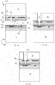
- FIG. 1a shows the starting point of a method for bonding and interconnecting two IC devices, hereafter referred to as chips.
- Two wafers 20a/20b are provided which are to be bonded in a wafer-to-wafer bonding technique.
- Each of the wafers comprises a semiconductor support substrate 1a/1b, e.g. a silicon substrate carrying at least one chip 10a/10b.
- These chips 10a/10b are to be bonded to form a 3D integrated device stack.
- the first chip 10a is to be bonded onto the second chip 10b.
- Both chips 10a/10b comprise a Front-End-Of-Line (FEOL) portion produced on the semiconductor substrate and a Back-End-Of-Line (BEOL) portion on the FEOL portion.
- FEOL Front-End-Of-Line
- BEOL Back-End-Of-Line
- FEOL refers to the part comprising active components such as transistors
- BEOL refers to the part comprising a metallization stack, i.e. a stack of dielectric layers (known as IMD, 'intermetal dielectric layers') with metal lines and via connections embedded therein, connecting the components of the FEOL portion to contact structures external to the chip.
- IMD dielectric layers
- BEOL refers to the part comprising a metallization stack, i.e. a stack of dielectric layers (known as IMD, 'intermetal dielectric layers') with metal lines and via connections embedded therein, connecting the components of the FEOL portion to contact structures external to the chip.
- IMD intermetal dielectric layers
- the second chip 10b furthermore comprises a redistribution layer 3b which is a further dielectric layer on top of the BEOL portion with metal contact structures embedded therein, with the latter contact structures being configured for connecting the chip to other contacts external to the chip.
- the redistribution layer 3b is shown as a separate layer for the sake of clarity but this layer may be part of the BEOL portion or may be a layer similar to a layer of the BEOL portion and produced in the same process sequence.
- the dielectric used in layer 3b may be a dielectric suitable for producing intermetal dielectric layers.
- the first chip 10a equally has a FEOL portion and a BEOL portion, drawn in this case as two layers 6a and 7a respectively, with a redistribution layer 3a in between the two.
- the redistribution layer is again drawn as a separate layer, but this may also be a layer that is similar to or a part of the BEOL portion 6a or of the FEOL portion 7a and that may be produced in one process sequence with one of these portions. So instead of being strictly FEOL, the portion 6a can be a layer comprising the FEOL portion of the chip and part of the BEOL portion.
- the contact structures 4a/4b may be contact pads that are part of the BEOL or FEOL portions.
- the dielectric of layer 3a is again preferably a material suitable for use as an intermetal dielectric.
- the metal contact structures in the embodiment shown in Figure 1a comprise metal contact pads 4a and 4b in the upper chip 10a and the lower chip 10b respectively, which are to be electrically connected by the method of the invention. Both pads may for example have a circular or polygon shaped surface.
- the upper pad 4a has an opening 15, preferably in the centre, for example a circular opening.
- the wafers 20a/20b are furthermore provided with dielectric bonding layers 5a/5b suitable for direct bonding.
- the dielectric material of the bonding layers may be silicon oxide, silicon carbon nitride (SiCN) or the bonding layers may comprise a stack of different materials.
- Direct bonding is a bonding technique known per se, wherein the bond is established by providing dielectric bonding layers on the two wafers, bringing these bonding layers into mutual contact and preferably applying an annealing step.
- the first chip 10a is provided with a cavity 16 in its outer surface, preferably having a circular cross-section.
- the cavity 16 traverses the dielectric bonding layer 5a, the BEOL portion 7a and the dielectric 3a within the opening 15.
- Cavity 16 may be produced by a suitable lithography and etch technique, for example a plasma etch applying the precursor C 4 F 8 in an oxygen and argon atmosphere. It is to be understood that the BEOL layers traversed by the cavity do not comprise semiconductor or metal materials at the location of the cavity, i.e. the cavity traverses only dielectric materials.
- the second chip 10b is provided with a metal contact pad 17 incorporated in the dielectric bonding layer 5b.
- the metal pad 17 is obtainable after producing the bonding layer 5b, by a single damascene process as known per se in the art.
- the metal pad 17 is in electrical contact with the contact pad 4b of the second chip 10b.
- the lateral dimensions of the metal pad 17 take into account the tolerance of the wafer-to-wafer alignment process so that when the wafers are aligned and bonded, the cavity 16 overlaps the metal pad 17.
- the totality of the cavity 16 is located within the boundaries of the metal pad 17, more preferably the two are essentially concentric as shown in the drawing.
- Hybrid bonding is a form of direct bonding wherein the dielectric bonding layers comprise metal areas with their outer surface essentially in the same plane as the outer surface of the bonding layer. Possibly, after polishing, the metal pad 17 may be slightly recessed with respect to the bonding layer 5b, e.g. by a distance of 5 to 10 nm.
- the wafers are positioned by aligning the metal contact pads 4a and 17/4b and the bonding layers 5a/5b are brought into mutual contact.
- An annealing step is preferably performed in order to establish a strong bond.
- the result is an assembly of the two wafers (referred to as the 'substrate assembly' in the appended claims) as shown in Figure 1b .
- This assembly is then subjected to a polishing step, to remove a portion of the top wafer's semiconductor substrate 1a, typically reducing this substrate to a thickness of less than 50micrometer.
- the result of this thinning step is illustrated in Figure 1c .
- a TSV opening 18 is etched through the back of the thinned upper semiconductor substrate 1a, and through the FEOL portion 6a of the upper chip 10a.
- the etching is stopped before reaching the metal contact pad 4a and thereby the cavity 16.
- the etching may be continued until reaching the cavity 16, as will be explained later in this description. Stopping short of the cavity is the preferred option, because it prevents sputtering of copper from the metal contact pad 4a at the end of the TSV etch.
- the TSV opening 18 is preferably a cylindrical opening with a given diameter.
- the litho/etch step involves producing a resist mask on the upper substrate 1a, etching the area not covered by the resist mask, followed by stripping of the resist.
- the TSV opening 18 is produced above the upper contact pad 4a that is provided with the opening 15 and with the cavity 16 through said opening.
- the cross section of the TSV opening 18 (in a plane parallel to the bonded wafers) overlaps the cross section (in the same plane) of the cavity 16.
- the cross-section of the TSV opening 18 is larger than the cross section of the cavity 16.
- the outer diameter of the contact pad 4a and of the opening 15 in the centre of the contact pad 4a are chosen with respect to the diameter of the TSV opening 18, and taking into account the tolerance on the alignment of the litho-mask for producing the TSV opening 18, so that that the cross section of the TSV opening 18 fully covers the circular opening 15 and a portion of the pad 4a itself, whilst staying within the outer boundaries of the contact pad 4a.
- the TSV opening 18 is concentric with the circular opening 15 and with the contact pad 4a itself.
- a conformal dielectric layer 19 is deposited on the upper surface of the thinned substrate 1a, the sidewalls of the TSV opening 18 and the bottom of said TSV opening 18, see Figure 1e .
- This conformal dielectric layer 19 is also known as a liner dielectric, hereafter referred to in short as the 'liner'. Its function is to isolate semiconductor material in the substrate 1a of the upper chip 10a from the metal contact plug that is to be formed in the TSV opening 18.
- the material and deposition technique for forming the liner is therefore also known to the skilled person.
- the liner may consist of or comprise SiO 2 , SiCO, SiN, SiCN or other suitable materials, deposited for example by Atomic Layer Deposition or Chemical Vapour Deposition (CVD).
- the liner 19 is subsequently removed from the bottom of the TSV opening 18 while on the sidewalls of the TSV opening, the liner remains at a thickness sufficient to perform the isolating function ( Figure 1f ).
- This is preferably achieved without a lithography step, i.e. without forming a photoresist mask or a hardmask that covers the sidewalls and exposes a portion of the bottom of the TSV opening 18.
- a preferred way of removing the liner 19 from the bottom of the TSV opening 18 while essentially maintaining the liner on the sidewalls is described in document EP3035369A1 . This method may be applied in any of the embodiments according to the present invention.
- a plasma etch is performed in an atmosphere comprising a polymer-forming component, so that a protective polymer is deposited on the sidewalls of the opening that allows removal of the liner from the bottom and any horizontal portions of the TSV opening during plasma etching, while protecting the sidewalls with the protective polymer.
- the plasma etch continues through the remaining layer of the FEOL portion 6a between the TSV opening 18 and the cavity 16.
- This remaining layer of material of the FEOL portion 6a is necessarily in this case a layer that comprises no semiconductor materials, given that the liner 19 will not cover the sidewalls of this area once the layer is removed.
- the remaining layer is typically an intermetal dielectric (IMD) layer.
- IMD intermetal dielectric
- the protective polymer layer (not shown) is then removed. This may be achieved by a treatment in an oxygen based plasma.
- the step of removing the protective polymer layer may advantageously be performed within the same plasma treatment tool where the previous plasma treatment was performed.
- the protective polymer layer may be removed using any suitable technique, such as wet etching or use of a dedicated remover.
- a seed layer and if required a barrier layer or an adhesive layer are deposited (not shown) on the interior surface of the aggregate opening 25, and the aggregate opening is filled with a metal, preferably by an electroplating step, preferably using copper as the deposited metal ( Figure 1g ).
- a metal plug 26 hereafter also referred to as TSV plug or TSV, or 'interconnection' plug, given its function as an electrical interconnection between the IC chips 10a and 10b.
- An alternative method is electroless deposition of metal, e.g. Cu or Ni or deposition of W by Chemical Vapour Deposition. After producing the TSV in this manner, the metal in the TSV opening may be recessed by a chemical mechanical polishing (CMP) step ( Figure 1h ).
- CMP chemical mechanical polishing
- the prior formation of the cavity 16 in the upper wafer 20a ensures that etching of the TSV opening 18 causes minimal or no damage to the contact pad 4a of the upper chip 10a, or sputtering of copper from this upper contact pad. This is the main advantage of any embodiment according to the invention.
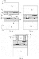
- an additional dielectric bonding layer 30 is applied on the lower wafer 20b, prior to the bonding step. This ensures that the bonding step is established by a 100% dielectric-to-dielectric bond, which is a higher quality bond than the hybrid bond obtained in the first embodiment.
- the presence of the extra bonding layer 30 does result in the requirement of an extra etching step for removing this bonding layer from the bottom of the aggregate opening 25, as illustrated in Figure 2c .
- This extra etching step may be the continuation of the etching process through the remaining part of the FEOL portion 6a between the TSV opening 18 and the cavity 16.
- the method according to the second embodiment comprises the same method steps and details as described above with respect to the first embodiment.
- the metal contact pad 4a of the upper chip 10a is not a copper contact pad or that it is a copper contact pad provided with a non-copper layer on the surface. This is to avoid or minimize copper sputtering during the removal of the additional dielectric bonding layer 30 at the bottom of the aggregate opening 25. It is advantageous in that regard to use a contact layer of the FEOL portion comprising Tungsten contact pads as the redistribution layer 3a. The use of tungsten in the FEOL portion is known per se in the art. Alternatively, copper contacts pads are generally provided with a stack of a TaN and Ta layer. When properly dimensioned, these layers can have the function of protecting the copper during etching of the additional dielectric bonding layer 30.
- the cavity 16 is not made through or adjacent to a metal contact pad in the upper chip. Instead, the cavity can be made anywhere on the surface of the upper chip 10a, while traversing the dielectric bonding layer 5a, the BEOL portion 7a and the dielectric of the redistribution layer 3a, see Figure 3a .
- a TSV can be produced that contacts the lower chip 10b only.
- the first chip 10a is aligned and bonded so that the cavity 16 overlaps the contact pad 17 of the lower chip 10b, taking into account the alignment tolerance, see Figure 3b .
- Etching the TSV opening 18 to create an aggregate opening with a liner 19 on the sidewalls is done in the same way as described above.
- a metal-filled TSV 26 is produced in the aggregate opening, contacting the metal contact pad 17 in the lower chip, see Figure 3c .
- the connection between the lower chip and the upper chip is then done by a second TSV 31 and a connection 32 as it is presently known in the art.
- the TSV 26 is still referred to as an 'interconnection' plug, as it forms part of the electrical path between the IC chips 10a and 10b.
- cavities can be produced in both wafers prior to the bonding step.
- This embodiment is illustrated in Figures 4a to 4c .
- the lower chip 10b has a cavity 35 in the dielectric bonding layer 5b, overlapping with the contact pad 4b of the lower chip.
- the cavity 35 is circular in cross section with a diameter that is preferably smaller than the cavity 16.
- the diameters of the two cavities is chosen so that taking into account the alignment tolerance, the larger cavity 16 fully covers the smaller cavity 35.
- the two cavities thereby form an aggregate cavity 36 after bonding, as shown in Figure 4b .
- the steps described with respect to the first embodiment are performed, leading to a TSV plug 26 as shown in Figure 4c , which interconnects the two chips 10a and 10b.
- a cavity is made in the surface of the upper chip prior to bonding, and that this cavity traverses at least the dielectric bonding layer 5a of the upper chip.
- the cavity traverses both the dielectric bonding layer and a number of additional dielectric layers underneath said bonding layer. If the cavity is limited to the bonding layer, the etching of the TSV opening will take longer and the risk of overetching and sputtering is still present, but to a lesser degree than in the presently existing methods.
- the aggregate opening is formed directly by the TSV etch, i.e. etching of the TSV opening continues until reaching the cavity 16 or 36.
- etching of the TSV opening continues until reaching the cavity 16 or 36.
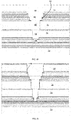
- Figure 5a to 5d shows the process stage where the same two chips 10a/10b as the ones shown in Figure 1 have been bonded by direct bonding, and wherein contrary to the process shown in Figure 1 , the TSV opening 18 is now etched through down to the cavity 16 to thereby create the aggregate opening 25.
- the liner 19 is now deposited on the sidewalls and the bottom of the aggregate opening 25, including on the horizontal parts 27 between the TSV opening 18 and the cavity 16, said horizontal parts comprising the exposed portions of the metal pad 4a of the upper chip.
- the plasma etch combined with the polymer-forming component as described above is applied and tuned to remove the liner from the bottom of the cavity 16 and from the horizontal parts 27, resulting in the situation shown in Figure 5c .
- This is followed by the creation of the metal plug 26, see Figure 5d , by the same method steps described in relation to the embodiment of Figure 1 .
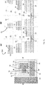
- Figures 6a to 6k illustrate how the method may be applied to interconnect more than two chips.
- Figure 6a shows a first and second wafer 20a/20b, consisting of substrates 1a/1b carrying chips 10a/10b which are to be bonded.
- the chips on both wafers are similar to the ones shown in Figure 1 : the first chip 10a has a perforated metal contact pad 4a, and a dielectric bonding layer 5a.
- the second chip 10b has a full metal contact pad 4b and a metal pad 17 incorporated in the bonding layer 5b.
- the first chip 10a further has a cavity 16 through the bonding layer, through part of the FEOL/BEOL part, indicated by a single numeral 2a and through the perforation of the metal contact pad 4a.
- the wafers are aligned and bonded, after which the upper substrate 1a is thinned and a passivation layer 40 and a bonding layer 41 are deposited on the thinned surface, see Figure 6b .
- a TSV opening 18 is made in the thinned surface, down to the cavity 16, see Figure 6c , thereby creating an aggregate opening 25.
- a third and fourth wafer 20c/20d consisting of substrates 1c/1d carrying a third and fourth chip 10c/10d are then provided, see Figure 6d , each of these chips having contact pads 4c/4d with central perforations.
- the inner diameter of the contact pad 4c in the third wafer is higher than the diameter of the TSV opening 18.
- the inner diameter of the contact pad 4d in the fourth chip 10d is higher than the inner diameter of the contact pad 4c in the third chip.
- Cavities 42/43 are produced in each of the third and fourth chip, respectively reaching down to the surface of the contact pad 4c and through the perforation of the contact pad 4d.
- the third and fourth wafer are aligned and bonded so as to form an aggregate cavity 44 and the top wafer is thinned and provided with a passivation and bonding layer 45/46, see Figure 6e .
- a further TSV opening 47 is produced through the thinned upper substrate 1c, see Figure 6f , and reaching down to the aggregate cavity 44, thereby forming a second aggregate opening consisting of the TSV opening 47 and the aggregate cavity 44.
- the upper substrate 1d is thinned and a passivation layer 50 is applied, Figure 6g .
- a final TSV opening 51 is etched in the thinned upper substrate 1d, see Figure 6h , landing on the contact pad of the upper chip 10d, and creating an aggregate opening 52 in the 4-wafer stack.
- a liner 19 is deposited on the side walls, the bottom and all the horizontal parts of the aggregate opening 52, see Figure 6i .
- the liner is removed from the bottom and from the horizontal parts by a plasma etch as described above, see Figure 6j .
- the aggregate opening is filled with a metal plug 62, see Figure 6k , by the same method steps as described in previous embodiments.
- the metal plug 62 interconnects the four chips 10a to 10d.
- the formation of the cavities 16, 42, 43 and the aggregate opening 44+47 prior to the respective bonding steps yields the advantage of the present invention, i.e. the minimization of overetching of metal contact pads and of damage by copper sputtering.
- a single additional substrate 1c could be bonded to the previously produced assembly of substrates 1a/1b, after forming a cavity in the additional substrate and aligning said cavity to the aggregate opening 25 in the assembly 1a/1b.
- the invention is not limited to cavities and/or TSV openings having a circular cross-section.
- the cross section of the TSV opening 18 is preferably larger than the cross section of the cavity 16. If this is not the case, the aggregate opening 25 may for example have a smaller cross-section at the top, and a larger cross section at the bottom. Also, it may be that the TSV opening 18 only partially overlaps the cavity 16. These conditions will make it more difficult to properly fill the aggregate opening with metal. Nevertheless, within limits it has been shown to be possible to fill such an opening so that a usable TSV plug is obtained.
- Figures 7a to 7d illustrate an embodiment wherein the cross section of the contact pads and of the cavities is rectangular and wherein a multiwafer stack is produced by addition of subsequent wafers, each wafer being provided with a cavity in accordance with the invention.
- Contact pads of subsequent substrates are arranged in step-wise fashion within a common TSV opening, allowing a single interconnect plug to interconnect a plurality of chips.
- 4 chips are interconnected.
- a top view of the contact pads and cavities is shown, as well as side views in two directions, to illustrate how the various levels may be interconnected.
- IMD dielectric layers bonding dielectric layers or the dielectric applied in redistribution layers. All dielectrics are marked by the same hatching type. In reality, this distinction remains the same as in the previously described embodiments.
- Figure 7a shows the situation after bonding of the first two wafers 20a and 20b and formation of a first TSV opening 18.
- Wafer 20a comprises semiconductor substrate 1a, carrying a first chip 10a and wafer 20b comprises semiconductor substrate 1b carrying a second chip 10b.
- the second chip 10b comprises a metal contact pad 17 embedded in a dielectric bonding layer.
- the metal pad 17 is in contact with a BEOL contact of the second chip (like contact 4b in previous embodiments), but such a BEOL contact is not shown in Figure 7a .
- the metal contact pad 17 has a rectangular cross-section, as shown in the top view.
- the first chip 10a has a contact pad 4a that is also rectangular-shaped.
- a rectangular cavity 16 is made in the first chip, with a depth d and placed adjacent to the contact pad 4a.
- the cavity 16 overlaps the contact pad 17 of the second chip 10b.
- a rectangular TSV opening 18 is formed in the second substrate 20b.
- the TSV opening 18 overlaps the cavity 16.
- the TSV opening's cross-section is larger than the cross-section of the cavity 16.
- Etching of the TSV opening 18 continues until an aggregate opening 25 is formed.
- the situation shown in Figure 7a could be followed by the liner deposition as described above, removal of the liner from the horizontal surfaces and formation of an interconnect plug that contacts the contact pads 4a and 17.
- a third wafer 20c is bonded to the stack of the first two wafers 20a/20b, after formation of the aggregate opening 25.
- the third wafer comprises semiconductor substrate 1c, carrying a third chip 10c comprising a rectangular contact pad 4c, and a rectangular cavity 70 adjacent to said contact pad 4c.
- the cavity 70 is etched in the third wafer before bonding the third wafer 20c to the stack of the first and second wafers 20a/20b.
- the bonding step results in the assembly of the three wafers 20a/20b/20c.
- the second cavity 70 overlaps the contact pads 17 and 4a in the second and first chip respectively.
- a second TSV opening 71 is then etched, the cross-section of the second TSV opening overlapping the contact pad 4c of the third substrate as well as the first and second cavities 16 and 70. The etching continues until a new aggregate opening 72 is formed.
- a fourth wafer 20d is added, comprising a fourth substrate 1d carrying a fourth chip 10d, having a further rectangular contact pad 4d and a third cavity 73 adjacent to said contact pad and etched in the fourth wafer before bonding this wafer to the assembly of the first to third wafers.
- a third TSV opening 74 is etched that overlaps the contact pad 4d of the fourth substrate as well as the first, second and third cavities 16, 70 and 73. The etching of the third TSV opening 74 continues until a final aggregate opening 75 is formed.
- the dimensions of the various contact pads, cavities and TSV openings takes into account the wafer-to-wafer alignment tolerance, the back-to-face accuracy of the through-semiconductor via etching applied for producing the TSV openings, and the thickness of the dielectric liner that is to be produced on the sidewalls of the aggregate openings. According to a preferred embodiment, these dimensions are chosen so that the contact area between the pads and the TSV plug is the same for all the levels in the stack.
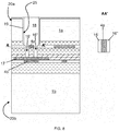
- FIG. 8 The second substrate 20b and the second chip 10b are the same as in the embodiment of Figure 1 .
- the contact pad 4a in the first chip 10a has a rectangular shape here, and two cavities 16' and 16" are etched on either side of the contact pad 4a, prior to bonding the first substrate 20a to the second substrate 20b.
- the cavities 16'/16" are located so that after bonding, they overlap with the contact pad 17 of the second chip 10b.
- the TSV opening 18 is etched in the same manner as in the embodiment of Figure 1 .
- the cross-section of the TSV opening 18 overlaps the cavities 16' and 16".
- This aggregate opening may then be filled with metal as described with respect to the previous embodiments.
- the cavity 16 is located in close proximity to the contact pad 4a of the first chip, and that the TSV opening 18 overlaps both the cavity 16 and the contact pad 4a of the first chip 10a.
- “In close proximity” means that the cavity is directly adjacent to the contact pad (as in Figure 7 ), or sufficiently close to allow that a single TSV opening is capable of overlapping both the cavity 16 and the contact pad 4a.
- the bottom of the cavity is preferably in the same plane as the upper plane of the contact pad 4a of the first chip (as seen in the assemblies shown in the drawings).
- the bottom of the cavity 16 is as close as possible to the upper or lower plane of the contact structure 4a of the upper chip in the assembly. In other words, the bottom of the cavity is in close proximity to the contact structure 4a of the upper chip.
- the description of a layer being present, deposited or produced 'on' another layer or substrate includes the options of
Landscapes
- Internal Circuitry In Semiconductor Integrated Circuit Devices (AREA)
- Engineering & Computer Science (AREA)
- Manufacturing & Machinery (AREA)
Claims (12)
- Verfahren zum Bonden und Verbinden einer ersten IC-Vorrichtung (10a), die auf einem ersten Substrat (1a) angeordnet ist, mit einer zweiten IC-Vorrichtung (10b), die auf einem zweiten Substrat (1b) angeordnet ist, wobei jede IC-Vorrichtung eine dielektrische Bondingschicht (5a, 5b) auf ihrer äußeren Oberfläche umfasst und wobei jede IC-Vorrichtung weiter eine oder mehrere Metallkontaktstrukturen (4a, 4b, 17) umfasst, wobei das Verfahren die Schritte umfasst:• Herstellen mindestens eines Hohlraums (16) in der äußeren Oberfläche der ersten IC-Vorrichtung (10a), wobei der Hohlraum mindestens die dielektrische Bondingschicht (5a) der ersten IC-Vorrichtung durchquert, und danach:• Ausrichten des ersten Substrats (1a) in Bezug auf das zweite Substrat (1b) und Bilden einer Substratanordnung durch direktes Bonden zwischen den Bondingschichten (5a, 5b), sodass in der Substratanordnung der Hohlraum (16), der in der ersten IC-Vorrichtung (10a) gebildet ist, eine Kontaktstruktur (4b, 17) der zweiten IC-Vorrichtung (10b) überlappt, und danach:• nach dem Bonden, optional Verdünnen des ersten Substrats (1a), und danach:• Herstellen einer Through Substrate Via (TSV) - Öffnung (18) in dem ersten Substrat (1a), wobei die TSV-Öffnung den Hohlraum (16) überlappt,• Bilden einer Aggregatöffnung (25), die die TSV-Öffnung (18) und den Hohlraum (16) umfasst, und dadurch Freilegen von mindestens einem Teil der Kontaktstruktur (4b, 17) der zweiten IC-Vorrichtung (10b),• nach dem Bilden eines Isolationsliners (19) auf mindestens einem Teil der Seitenwände der Aggregatöffnung (25), Herstellen eines Metallverbindungssteckers (26) in der Aggregatöffnung, der die Kontaktstruktur (4b, 17) der zweiten IC-Vorrichtung (10b) kontaktiert und mindestens einen Teil eines Verbindungspfads zwischen der Kontaktstruktur der zweiten IC-Vorrichtung (10b) und einer Kontaktstruktur der ersten IC-Vorrichtung (10a) bildet,wobei:• die zweite IC-Vorrichtung (10b) ein Metallkontaktpad (17) umfasst, das in der Bondingschicht (5b) der zweiten Vorrichtung eingearbeitet ist, sodass die obere Oberfläche des Metallkontaktpads (17) im Wesentlichen in derselben Ebene wie die obere Oberfläche der Bondingschicht (5b) liegt,• das Metallkontaktpad (17) in elektrischem Kontakt mit einer Metallkontaktstruktur (4b) der zweiten IC-Vorrichtung (10b) steht und• in der Substratanordnung der Hohlraum (16) das Metallkontaktpad (17) überlappt, und dadurch gekennzeichnet, dass• eine zusätzliche dielektrische Bondingschicht (30) auf der Bondingschicht (5b) vorhanden ist, in die das Metallkontaktpad (17) eingearbeitet ist, und• die Bildung der Aggregatöffnung (25) einen Schritt eines Ätzens durch die zusätzliche dielektrische Bondingschicht (30) in dem Bereich der zusätzlichen Schicht (30), die den Hohlraum (16) überlappt, einschließt.
- Verfahren nach Anspruch 1, wobei die erste IC-Vorrichtung (10a) einen Stapel von dielektrischen Schichten (2a, 6a, 7a, 3a) umfasst, bei dem die Bondingschicht (5a) obenauf auf dem Stapel von dielektrischen Schichten vorhanden ist und wobei der Hohlraum (16) weiter eine oder mehrere aus dem Stapel von dielektrischen Schichten durchquert.
- Verfahren nach Anspruch 2, wobei die erste IC-Vorrichtung (10a) einen Front-End-Of-Line-Abschnitt (6a) und einen Back-End-Of-Line (BEOL) - Abschnitt (7a) umfasst und wobei der Stapel von dielektrischen Schichten ein Stapel von zwischenmetallischen dielektrischen Schichten in dem BEOL-Abschnitt (7a) oder in dem BEOL-Abschnitt (7a) wie auch in dem FEOL-Abschnitt (6a) der ersten IC-Vorrichtung (10a) ist.
- Verfahren nach einem der Ansprüche 1 bis 3, wobei sich der Hohlraum (16) in enger Nähe zu einer Metallkontaktstruktur (4a) der ersten IC-Vorrichtung (10a) befindet und wobei die TSV-Öffnung (18) die Kontaktstruktur (4a) der ersten IC-Vorrichtung überlappt, sodass der Verbindungsstecker (26) die Kontaktstruktur (4a) der ersten IC-Vorrichtung (10a) mit der Kontaktstruktur (17, 4b) der zweiten IC-Vorrichtung (10b) verbindet.
- Verfahren nach Anspruch 4, wobei die Metallkontaktstruktur (4a) in der ersten IC-Vorrichtung (10a) ein Metallkontaktpad ist, das Teil des FEOL-Abschnitts (6a) oder des BEOL-Abschnitts (7a) der ersten IC-Vorrichtung (10a) ist.
- Verfahren nach Anspruch 4 oder 5, wobei• die Kontaktstruktur der ersten IC-Vorrichtung (10a) ein Metallpad (4a) mit einem zentral platzierten offenen Bereich (15) ist und• der Hohlraum (16) der ersten Vorrichtung (10a) mindestens teilweise den offenen Bereich durchquert.
- Verfahren nach Anspruch 4 oder 5, wobei die Kontaktstruktur der ersten IC-Vorrichtung (10a) ein Metallpad (4a) mit einem polygonförmigen Querschnitt in der Ebene des Kontaktpads ist und wobei sich der Boden des Hohlraums (16) in enger Nähe zu dem polygonförmigen Metallpad (4a) befindet.
- Verfahren nach einem der vorstehenden Ansprüche, wobei:• die Prozedur, die zum Herstellen der TSV-Öffnung (18) angewandt wird, vor Erreichen des Hohlraums (16) angehalten wird, was eine Schicht von verbleibendem dielektrischen Material zwischen der TSV-Öffnung und dem Hohlraum belässt, und danach:• der Isolierungsliner (19) auf den Seitenwänden und dem Boden der TSV-Öffnung (18) angebracht wird, gefolgt durch den Schritt eines Entfernen des Isolierungsliners von dem Boden der TSV-Öffnung, und danach:• die Schicht von verbleibendem Material zwischen der TSV-Öffnung und dem Hohlraum gleichsam beim Bilden der Aggregatöffnung (25) entfernt wird.
- Verfahren nach einem der Ansprüche 1 bis 7, wobei• die Prozedur, die zum Herstellen der TSV-Öffnung (18) angewandt wird, fortgesetzt wird, bis der Hohlraum (16) erreicht ist, wodurch die Aggregatöffnung (25) gebildet wird, und danach• der Isolationsliner (19) auf den Seitenwänden, dem Boden und horizontalen Abschnitten (27) der Aggregatöffnung (25) angebracht wird, und danach• der Isolationsliner (19) von dem Boden und von den horizontalen Abschnitten der Aggregatöffnung vor Herstellen des Verbindungssteckers (26) entfernt wird.
- Verfahren nach einem der vorstehenden Ansprüche, wobei:• nach dem Bilden der TSV-Öffnung (18) ein zusätzliches Substrat (1c) oder ein Stapel von zusätzlichen Substraten (1c, 1d) an die Substratanordnung gebondet wird, wobei jedes zusätzliche Substrat eine zusätzliche IC-Vorrichtung (10c, 10d) trägt,• das zusätzliche Substrat oder der Stapel von zusätzlichen Substraten mit einem zweiten Hohlraum (44+47; 70) in seiner Bondingoberfläche bereitgestellt wird, vor Bonden des zusätzlichen Substrats oder Stapels von Substraten an die Anordnung, sodass der Bondingschritt in einer neuen Anordnung resultiert, in der der zweite Hohlraum (44+47; 70) die TSV-Öffnung (18) überlappt,• danach eine zweite TSV-Öffnung (51, 71) in der neuen Anordnung hergestellt wird, wobei die zweite TSV-Öffnung den zweiten Hohlraum überlappt, wodurch eine neue Aggregatöffnung (52; 72) gebildet wird, die den Hohlraum (16) in der ersten IC-Vorrichtung, die TSV-Öffnung (18), den zweiten Hohlraum (44+47; 70) und die zweite TSV-Öffnung (51, 71) umfasst,• optional die vorherigen Schritte einmal oder mehrfach wiederholt werden, jedes Mal unter Hinzufügen eines weiteren Substrats oder Stapels von Substraten zu der Anordnung, und führend zu einer finalen Anordnung, die eine finale Aggregatöffnung (52, 75) umfasst,• nach der Bildung eines Isolationsliners (19) auf mindestens einem Teil der Seitenwände der finalen Aggregatöffnung (25, 72) ein Metallverbindungsstecker (26) in der finalen Aggregatöffnung hergestellt wird, der die Kontaktstruktur (4b, 17) der zweiten IC-Vorrichtung (10b) kontaktiert.
- Verfahren nach Anspruch 10, wobei ein Stapel von zwei zusätzlichen Substraten (1c, 1d) an die Substratanordnung gebondet wird und wobei der Stapel durch Bonden des ersten zusätzlichen Substrats (1c) an das zweite zusätzliche Substrat (1d) in Übereinstimmung mit einem Hilfsverfahren zum Bonden und Verbinden einer ersten IC-Vorrichtung (10c), die auf einem ersten Substrat (1c) angeordnet ist, mit einer zweiten IC-Vorrichtung (10d), die auf einem zweiten Substrat (1d) angeordnet ist, erhalten wird, wobei jede IC-Vorrichtung eine dielektrische Bondingschicht auf ihrer äußeren Oberfläche umfasst und wobei jede IC-Vorrichtung weiter eine oder mehrere Metallkontaktstrukturen (4c, 4d) umfasst, wobei das Hilfsverfahren die Schritte umfasst:• Herstellen mindestens eines Hohlraums (42) in der äußeren Oberfläche der ersten IC-Vorrichtung (10c), wobei der Hohlraum mindestens die dielektrische Bondingschicht der ersten IC-Vorrichtung durchquert, und danach:• Ausrichten des ersten Substrats (1c) in Bezug auf das zweite Substrat (1d) und Bilden einer Substratanordnung durch direktes Bonden zwischen den Bondingschichten, sodass in der Substratanordnung der Hohlraum (42), der in der ersten IC-Vorrichtung (10c) gebildet ist, eine Kontaktstruktur (4d) der zweiten IC-Vorrichtung (10d) überlappt, und danach:• nach dem Bonden, optional Verdünnen des ersten Substrats, und danach:• Herstellen einer Through Substrate Via (TSV) - Öffnung (47) in dem ersten Substrat, wobei die TSV-Öffnung den Hohlraum (42) überlappt,• Bilden einer Aggregatöffnung, die die TSV-Öffnung und den Hohlraum umfasst, und dadurch Freilegen von mindestens einem Teil der Kontaktstruktur (4d) der zweiten IC-Vorrichtung,• nach dem Bilden eines Isolationsliners (19) auf mindestens einem Teil der Seitenwände der Aggregatöffnung, Herstellen eines Metallverbindungssteckers (62) in der Aggregatöffnung, der die Kontaktstruktur der zweiten IC-Vorrichtung kontaktiert und mindestens einen Teil eines Verbindungspfads zwischen der Kontaktstruktur der zweiten IC-Vorrichtung und einer Kontaktstruktur der ersten IC-Vorrichtung bildet, und wobei nach dem Hilfsverfahren die zweite IC-Vorrichtung gleichsam mit einem Hohlraum (43) in der äußeren Oberfläche der Vorrichtung bereitgestellt wird, wobei der Hohlraum mindestens die Bondingschicht der zweiten Vorrichtung durchquert, wobei der Hohlraum (43) der zweiten Vorrichtung die Metallkontaktstruktur (4d) der zweiten Vorrichtung überlappt, und wobei Bonding derart durchgeführt wird, dass sich beide Hohlräume (42, 43) in der Substratanordnung überlappen, um einen Aggregathohlraum (44) nach dem Bonden zu bilden, um einen Stapel zu erhalten, der einen Aggregathohlraum (44) umfasst, und wobei eine zusätzliche TSV-Öffnung (47) in der Bondingoberfläche des Stapels hergestellt wird, um dadurch einen Stapel mit dem zweiten Hohlraum in seiner äußeren Oberfläche zu erhalten, wobei der zweite Hohlraum durch den Aggregathohlraum (44) und die zusätzliche TSV-Öffnung (47) gebildet ist.
- Verfahren nach Anspruch 10 oder 11, wobei jede der IC-Vorrichtungen (10a, 10b, 10c, 10d) in der finalen Anordnung eine Kontaktstruktur (4a, 4b/17, 4c, 4d) umfasst, die durch den Verbindungsstecker (26) kontaktiert wird, der in der finalen Aggregatöffnung (52, 72) gebildet ist.
Priority Applications (3)
| Application Number | Priority Date | Filing Date | Title |
|---|---|---|---|
| EP16187668.5A EP3293757B1 (de) | 2016-09-07 | 2016-09-07 | Verfahren zum bonden und verbinden von integrierten schaltungsvorrichtungen |
| EP19166953.0A EP3531445B1 (de) | 2016-09-07 | 2016-09-07 | Verfahren zum bonden und verbinden von integrierten schaltungsvorrichtungen |
| US15/697,285 US10170450B2 (en) | 2016-09-07 | 2017-09-06 | Method for bonding and interconnecting integrated circuit devices |
Applications Claiming Priority (1)
| Application Number | Priority Date | Filing Date | Title |
|---|---|---|---|
| EP16187668.5A EP3293757B1 (de) | 2016-09-07 | 2016-09-07 | Verfahren zum bonden und verbinden von integrierten schaltungsvorrichtungen |
Related Child Applications (1)
| Application Number | Title | Priority Date | Filing Date |
|---|---|---|---|
| EP19166953.0A Division EP3531445B1 (de) | 2016-09-07 | 2016-09-07 | Verfahren zum bonden und verbinden von integrierten schaltungsvorrichtungen |
Publications (2)
| Publication Number | Publication Date |
|---|---|
| EP3293757A1 EP3293757A1 (de) | 2018-03-14 |
| EP3293757B1 true EP3293757B1 (de) | 2019-04-17 |
Family
ID=56883727
Family Applications (2)
| Application Number | Title | Priority Date | Filing Date |
|---|---|---|---|
| EP19166953.0A Active EP3531445B1 (de) | 2016-09-07 | 2016-09-07 | Verfahren zum bonden und verbinden von integrierten schaltungsvorrichtungen |
| EP16187668.5A Not-in-force EP3293757B1 (de) | 2016-09-07 | 2016-09-07 | Verfahren zum bonden und verbinden von integrierten schaltungsvorrichtungen |
Family Applications Before (1)
| Application Number | Title | Priority Date | Filing Date |
|---|---|---|---|
| EP19166953.0A Active EP3531445B1 (de) | 2016-09-07 | 2016-09-07 | Verfahren zum bonden und verbinden von integrierten schaltungsvorrichtungen |
Country Status (2)
| Country | Link |
|---|---|
| US (1) | US10170450B2 (de) |
| EP (2) | EP3531445B1 (de) |
Families Citing this family (27)
| Publication number | Priority date | Publication date | Assignee | Title |
|---|---|---|---|---|
| US9953941B2 (en) | 2015-08-25 | 2018-04-24 | Invensas Bonding Technologies, Inc. | Conductive barrier direct hybrid bonding |
| CN107492533B (zh) * | 2016-06-12 | 2020-03-10 | 中芯国际集成电路制造(上海)有限公司 | 封装结构及其封装方法 |
| WO2019241367A1 (en) * | 2018-06-12 | 2019-12-19 | Invensas Bonding Technologies, Inc. | Interlayer connection of stacked microelectronic components |
| US12406959B2 (en) | 2018-07-26 | 2025-09-02 | Adeia Semiconductor Bonding Technologies Inc. | Post CMP processing for hybrid bonding |
| CN109148415B (zh) * | 2018-08-28 | 2020-08-25 | 武汉新芯集成电路制造有限公司 | 多晶圆堆叠结构及其形成方法 |
| KR102593085B1 (ko) | 2018-11-21 | 2023-10-24 | 삼성전자주식회사 | 반도체 장치, 반도체 패키지 및 이의 제조 방법 |
| KR102756185B1 (ko) | 2019-03-15 | 2025-01-17 | 삼성전자주식회사 | 디스플레이 드라이버 ic 소자 |
| US11217547B2 (en) * | 2019-09-03 | 2022-01-04 | Taiwan Semiconductor Manufacturing Company, Ltd. | Bond pad structure with reduced step height and increased electrical isolation |
| JP2021044498A (ja) * | 2019-09-13 | 2021-03-18 | キオクシア株式会社 | 半導体装置の製造方法 |
| US11164749B1 (en) * | 2019-09-16 | 2021-11-02 | Xilinx, Inc. | Warpage reduction |
| WO2021208078A1 (zh) * | 2020-04-17 | 2021-10-21 | 华为技术有限公司 | 一种半导体结构及其制造方法 |
| US11315904B2 (en) * | 2020-05-15 | 2022-04-26 | Nanya Technology Corporation | Semiconductor assembly and method of manufacturing the same |
| DE102020126211A1 (de) * | 2020-05-28 | 2021-12-02 | Taiwan Semiconductor Manufacturing Co. Ltd. | Photolithographie-Ausrichtungsprozess für gebondete Wafer |
| US11502038B2 (en) * | 2020-08-03 | 2022-11-15 | Nanya Technology Corporation | Semiconductor structure having via through bonded wafers and manufacturing method thereof |
| US20220084884A1 (en) | 2020-09-15 | 2022-03-17 | Nanya Technology Corporation | Semiconductor structure and method of forming the same |
| US20220084948A1 (en) | 2020-09-17 | 2022-03-17 | Nanya Technology Corporation | Semiconductor structure and manufacturing method thereof |
| US11610833B2 (en) * | 2020-10-22 | 2023-03-21 | Nanya Technology Corporation | Conductive feature with non-uniform critical dimension and method of manufacturing the same |
| US11355464B2 (en) * | 2020-11-10 | 2022-06-07 | Nanya Technology Corporation | Semiconductor device structure with bottle-shaped through silicon via and method for forming the same |
| CN113013094B (zh) * | 2021-02-24 | 2023-07-07 | 长江存储科技有限责任公司 | 一种半导体器件及其制造方法 |
| US11664364B2 (en) * | 2021-03-25 | 2023-05-30 | Nanya Technology Corporation | Semiconductor device with through semiconductor via and method for fabricating the same |
| EP4207262B1 (de) | 2021-07-09 | 2025-04-23 | Changxin Memory Technologies, Inc. | Halbleiterstruktur und herstellungsverfahren dafür |
| CN115602610B (zh) * | 2021-07-09 | 2025-08-08 | 长鑫存储技术有限公司 | 半导体结构及其制备方法 |
| CN113795916B (zh) * | 2021-08-05 | 2024-05-28 | 广东省科学院半导体研究所 | 芯片堆叠封装结构及芯片堆叠封装方法 |
| CN116417403A (zh) * | 2021-12-30 | 2023-07-11 | 联华电子股份有限公司 | 半导体元件及其制作方法 |
| US20240006332A1 (en) * | 2022-07-01 | 2024-01-04 | Intel Corporation | Fiducial marks for verifying alignment accuracy of bonded integrated circuit dies |
| US20240079325A1 (en) * | 2022-09-01 | 2024-03-07 | International Business Machines Corporation | Hybrid backside dielectric for clock and power wires |
| US20250167109A1 (en) * | 2023-11-20 | 2025-05-22 | Globalfoundries Singapore Pte. Ltd. | Stacked semiconductor structures including a passive device |
Family Cites Families (12)
| Publication number | Priority date | Publication date | Assignee | Title |
|---|---|---|---|---|
| US7485968B2 (en) | 2005-08-11 | 2009-02-03 | Ziptronix, Inc. | 3D IC method and device |
| US7855455B2 (en) * | 2008-09-26 | 2010-12-21 | International Business Machines Corporation | Lock and key through-via method for wafer level 3 D integration and structures produced |
| US9064717B2 (en) * | 2008-09-26 | 2015-06-23 | International Business Machines Corporation | Lock and key through-via method for wafer level 3D integration and structures produced thereby |
| US7939369B2 (en) * | 2009-05-14 | 2011-05-10 | International Business Machines Corporation | 3D integration structure and method using bonded metal planes |
| TWI402941B (zh) * | 2009-12-03 | 2013-07-21 | 日月光半導體製造股份有限公司 | 半導體結構及其製造方法 |
| CN102226999B (zh) * | 2011-05-11 | 2014-04-23 | 迈尔森电子(天津)有限公司 | 衬底结构及其制作方法 |
| US9576889B2 (en) * | 2012-06-25 | 2017-02-21 | Research Triangle Institute | Three-dimensional electronic packages utilizing unpatterned adhesive layer |
| DE102012108522A1 (de) * | 2012-09-12 | 2014-03-13 | Ams Ag | Verfahren zur Herstellung eines Halbleiterstapels und Halbleiterstapel mit rückseitigem Durchkontakt |
| US9041206B2 (en) | 2013-03-12 | 2015-05-26 | Taiwan Semiconductor Manufacturing Company, Ltd. | Interconnect structure and method |
| US9293437B2 (en) | 2014-02-20 | 2016-03-22 | Taiwan Semiconductor Manufacturing Company, Ltd. | Functional block stacked 3DIC and method of making same |
| EP3035369B1 (de) | 2014-12-18 | 2020-11-25 | IMEC vzw | Plasmabehandlungsverfahren |
| EP3113216B1 (de) * | 2015-07-01 | 2021-05-19 | IMEC vzw | Verfahren zum befestigen und verbinden von integrierten schaltungsvorrichtungen |
-
2016
- 2016-09-07 EP EP19166953.0A patent/EP3531445B1/de active Active
- 2016-09-07 EP EP16187668.5A patent/EP3293757B1/de not_active Not-in-force
-
2017
- 2017-09-06 US US15/697,285 patent/US10170450B2/en active Active
Non-Patent Citations (1)
| Title |
|---|
| None * |
Also Published As
| Publication number | Publication date |
|---|---|
| US10170450B2 (en) | 2019-01-01 |
| EP3293757A1 (de) | 2018-03-14 |
| US20180068984A1 (en) | 2018-03-08 |
| EP3531445A1 (de) | 2019-08-28 |
| EP3531445B1 (de) | 2020-06-24 |
Similar Documents
| Publication | Publication Date | Title |
|---|---|---|
| US10170450B2 (en) | Method for bonding and interconnecting integrated circuit devices | |
| US11004832B2 (en) | System, structure, and method of manufacturing a semiconductor substrate stack | |
| JP2024524391A (ja) | 接合層内にルーティング構造体を有する素子 | |
| KR101137624B1 (ko) | 비아 구조 및 그것을 형성하는 비아에칭 방법 | |
| JP5201048B2 (ja) | 半導体装置とその製造方法 | |
| JP5345077B2 (ja) | 低k誘電体ライナーを有するシリコン貫通ビア | |
| EP2255386B1 (de) | Verfahren zur Herstellung von Substratdurchkontaktierungen und für Durchkontaktierungen vorbereiteter Halbleiterchip | |
| TWI807331B (zh) | 半導體結構及其製造方法 | |
| CN101794717B (zh) | 堆叠集成芯片及其制造方法 | |
| TWI429046B (zh) | 半導體裝置及其製造方法 | |
| US20090212438A1 (en) | Integrated circuit device comprising conductive vias and method of making the same | |
| TW201023331A (en) | Semiconductor device and method for forming the same | |
| TW201214622A (en) | Method for forming a through-substrate via (TSV) | |
| EP3171399B1 (de) | Verfahren zur vereinzelung eines stapels von halbleiterwafern | |
| US9401323B1 (en) | Protected through semiconductor via (TSV) | |
| EP3671812B1 (de) | Verfahren zum bonden und verbinden von halbleiterchips | |
| JP2008085226A (ja) | 半導体ウェハおよびその製造方法、ならびに半導体装置の製造方法 | |
| US11315904B2 (en) | Semiconductor assembly and method of manufacturing the same | |
| CN117276194A (zh) | 半导体制造方法及半导体结构 | |
| CN111834313A (zh) | 一种有源芯片高密度tsv结构及制作方法 |
Legal Events
| Date | Code | Title | Description |
|---|---|---|---|
| PUAI | Public reference made under article 153(3) epc to a published international application that has entered the european phase |
Free format text: ORIGINAL CODE: 0009012 |
|
| STAA | Information on the status of an ep patent application or granted ep patent |
Free format text: STATUS: THE APPLICATION HAS BEEN PUBLISHED |
|
| AK | Designated contracting states |
Kind code of ref document: A1 Designated state(s): AL AT BE BG CH CY CZ DE DK EE ES FI FR GB GR HR HU IE IS IT LI LT LU LV MC MK MT NL NO PL PT RO RS SE SI SK SM TR |
|
| AX | Request for extension of the european patent |
Extension state: BA ME |
|
| STAA | Information on the status of an ep patent application or granted ep patent |
Free format text: STATUS: REQUEST FOR EXAMINATION WAS MADE |
|
| 17P | Request for examination filed |
Effective date: 20180910 |
|
| RBV | Designated contracting states (corrected) |
Designated state(s): AL AT BE BG CH CY CZ DE DK EE ES FI FR GB GR HR HU IE IS IT LI LT LU LV MC MK MT NL NO PL PT RO RS SE SI SK SM TR |
|
| GRAP | Despatch of communication of intention to grant a patent |
Free format text: ORIGINAL CODE: EPIDOSNIGR1 |
|
| STAA | Information on the status of an ep patent application or granted ep patent |
Free format text: STATUS: GRANT OF PATENT IS INTENDED |
|
| INTG | Intention to grant announced |
Effective date: 20181105 |
|
| GRAS | Grant fee paid |
Free format text: ORIGINAL CODE: EPIDOSNIGR3 |
|
| GRAA | (expected) grant |
Free format text: ORIGINAL CODE: 0009210 |
|
| STAA | Information on the status of an ep patent application or granted ep patent |
Free format text: STATUS: THE PATENT HAS BEEN GRANTED |
|
| AK | Designated contracting states |
Kind code of ref document: B1 Designated state(s): AL AT BE BG CH CY CZ DE DK EE ES FI FR GB GR HR HU IE IS IT LI LT LU LV MC MK MT NL NO PL PT RO RS SE SI SK SM TR |
|
| REG | Reference to a national code |
Ref country code: GB Ref legal event code: FG4D |
|
| REG | Reference to a national code |
Ref country code: CH Ref legal event code: EP |
|
| REG | Reference to a national code |
Ref country code: DE Ref legal event code: R096 Ref document number: 602016012480 Country of ref document: DE |
|
| REG | Reference to a national code |
Ref country code: AT Ref legal event code: REF Ref document number: 1122490 Country of ref document: AT Kind code of ref document: T Effective date: 20190515 Ref country code: IE Ref legal event code: FG4D |
|
| REG | Reference to a national code |
Ref country code: NL Ref legal event code: MP Effective date: 20190417 |
|
| REG | Reference to a national code |
Ref country code: LT Ref legal event code: MG4D |
|
| PG25 | Lapsed in a contracting state [announced via postgrant information from national office to epo] |
Ref country code: NL Free format text: LAPSE BECAUSE OF FAILURE TO SUBMIT A TRANSLATION OF THE DESCRIPTION OR TO PAY THE FEE WITHIN THE PRESCRIBED TIME-LIMIT Effective date: 20190417 |
|
| PG25 | Lapsed in a contracting state [announced via postgrant information from national office to epo] |
Ref country code: ES Free format text: LAPSE BECAUSE OF FAILURE TO SUBMIT A TRANSLATION OF THE DESCRIPTION OR TO PAY THE FEE WITHIN THE PRESCRIBED TIME-LIMIT Effective date: 20190417 Ref country code: HR Free format text: LAPSE BECAUSE OF FAILURE TO SUBMIT A TRANSLATION OF THE DESCRIPTION OR TO PAY THE FEE WITHIN THE PRESCRIBED TIME-LIMIT Effective date: 20190417 Ref country code: LT Free format text: LAPSE BECAUSE OF FAILURE TO SUBMIT A TRANSLATION OF THE DESCRIPTION OR TO PAY THE FEE WITHIN THE PRESCRIBED TIME-LIMIT Effective date: 20190417 Ref country code: NO Free format text: LAPSE BECAUSE OF FAILURE TO SUBMIT A TRANSLATION OF THE DESCRIPTION OR TO PAY THE FEE WITHIN THE PRESCRIBED TIME-LIMIT Effective date: 20190717 Ref country code: PT Free format text: LAPSE BECAUSE OF FAILURE TO SUBMIT A TRANSLATION OF THE DESCRIPTION OR TO PAY THE FEE WITHIN THE PRESCRIBED TIME-LIMIT Effective date: 20190817 Ref country code: FI Free format text: LAPSE BECAUSE OF FAILURE TO SUBMIT A TRANSLATION OF THE DESCRIPTION OR TO PAY THE FEE WITHIN THE PRESCRIBED TIME-LIMIT Effective date: 20190417 Ref country code: AL Free format text: LAPSE BECAUSE OF FAILURE TO SUBMIT A TRANSLATION OF THE DESCRIPTION OR TO PAY THE FEE WITHIN THE PRESCRIBED TIME-LIMIT Effective date: 20190417 Ref country code: SE Free format text: LAPSE BECAUSE OF FAILURE TO SUBMIT A TRANSLATION OF THE DESCRIPTION OR TO PAY THE FEE WITHIN THE PRESCRIBED TIME-LIMIT Effective date: 20190417 |
|
| PG25 | Lapsed in a contracting state [announced via postgrant information from national office to epo] |
Ref country code: LV Free format text: LAPSE BECAUSE OF FAILURE TO SUBMIT A TRANSLATION OF THE DESCRIPTION OR TO PAY THE FEE WITHIN THE PRESCRIBED TIME-LIMIT Effective date: 20190417 Ref country code: PL Free format text: LAPSE BECAUSE OF FAILURE TO SUBMIT A TRANSLATION OF THE DESCRIPTION OR TO PAY THE FEE WITHIN THE PRESCRIBED TIME-LIMIT Effective date: 20190417 Ref country code: GR Free format text: LAPSE BECAUSE OF FAILURE TO SUBMIT A TRANSLATION OF THE DESCRIPTION OR TO PAY THE FEE WITHIN THE PRESCRIBED TIME-LIMIT Effective date: 20190718 Ref country code: RS Free format text: LAPSE BECAUSE OF FAILURE TO SUBMIT A TRANSLATION OF THE DESCRIPTION OR TO PAY THE FEE WITHIN THE PRESCRIBED TIME-LIMIT Effective date: 20190417 Ref country code: BG Free format text: LAPSE BECAUSE OF FAILURE TO SUBMIT A TRANSLATION OF THE DESCRIPTION OR TO PAY THE FEE WITHIN THE PRESCRIBED TIME-LIMIT Effective date: 20190717 |
|
| REG | Reference to a national code |
Ref country code: AT Ref legal event code: MK05 Ref document number: 1122490 Country of ref document: AT Kind code of ref document: T Effective date: 20190417 |
|
| PG25 | Lapsed in a contracting state [announced via postgrant information from national office to epo] |
Ref country code: IS Free format text: LAPSE BECAUSE OF FAILURE TO SUBMIT A TRANSLATION OF THE DESCRIPTION OR TO PAY THE FEE WITHIN THE PRESCRIBED TIME-LIMIT Effective date: 20190817 |
|
| REG | Reference to a national code |
Ref country code: DE Ref legal event code: R097 Ref document number: 602016012480 Country of ref document: DE |
|
| PG25 | Lapsed in a contracting state [announced via postgrant information from national office to epo] |
Ref country code: RO Free format text: LAPSE BECAUSE OF FAILURE TO SUBMIT A TRANSLATION OF THE DESCRIPTION OR TO PAY THE FEE WITHIN THE PRESCRIBED TIME-LIMIT Effective date: 20190417 Ref country code: CZ Free format text: LAPSE BECAUSE OF FAILURE TO SUBMIT A TRANSLATION OF THE DESCRIPTION OR TO PAY THE FEE WITHIN THE PRESCRIBED TIME-LIMIT Effective date: 20190417 Ref country code: EE Free format text: LAPSE BECAUSE OF FAILURE TO SUBMIT A TRANSLATION OF THE DESCRIPTION OR TO PAY THE FEE WITHIN THE PRESCRIBED TIME-LIMIT Effective date: 20190417 Ref country code: AT Free format text: LAPSE BECAUSE OF FAILURE TO SUBMIT A TRANSLATION OF THE DESCRIPTION OR TO PAY THE FEE WITHIN THE PRESCRIBED TIME-LIMIT Effective date: 20190417 Ref country code: SK Free format text: LAPSE BECAUSE OF FAILURE TO SUBMIT A TRANSLATION OF THE DESCRIPTION OR TO PAY THE FEE WITHIN THE PRESCRIBED TIME-LIMIT Effective date: 20190417 Ref country code: DK Free format text: LAPSE BECAUSE OF FAILURE TO SUBMIT A TRANSLATION OF THE DESCRIPTION OR TO PAY THE FEE WITHIN THE PRESCRIBED TIME-LIMIT Effective date: 20190417 |
|
| PLBE | No opposition filed within time limit |
Free format text: ORIGINAL CODE: 0009261 |
|
| STAA | Information on the status of an ep patent application or granted ep patent |
Free format text: STATUS: NO OPPOSITION FILED WITHIN TIME LIMIT |
|
| PG25 | Lapsed in a contracting state [announced via postgrant information from national office to epo] |
Ref country code: IT Free format text: LAPSE BECAUSE OF FAILURE TO SUBMIT A TRANSLATION OF THE DESCRIPTION OR TO PAY THE FEE WITHIN THE PRESCRIBED TIME-LIMIT Effective date: 20190417 Ref country code: SM Free format text: LAPSE BECAUSE OF FAILURE TO SUBMIT A TRANSLATION OF THE DESCRIPTION OR TO PAY THE FEE WITHIN THE PRESCRIBED TIME-LIMIT Effective date: 20190417 |
|
| 26N | No opposition filed |
Effective date: 20200120 |
|
| PG25 | Lapsed in a contracting state [announced via postgrant information from national office to epo] |
Ref country code: TR Free format text: LAPSE BECAUSE OF FAILURE TO SUBMIT A TRANSLATION OF THE DESCRIPTION OR TO PAY THE FEE WITHIN THE PRESCRIBED TIME-LIMIT Effective date: 20190417 |
|
| PG25 | Lapsed in a contracting state [announced via postgrant information from national office to epo] |
Ref country code: SI Free format text: LAPSE BECAUSE OF FAILURE TO SUBMIT A TRANSLATION OF THE DESCRIPTION OR TO PAY THE FEE WITHIN THE PRESCRIBED TIME-LIMIT Effective date: 20190417 Ref country code: MC Free format text: LAPSE BECAUSE OF FAILURE TO SUBMIT A TRANSLATION OF THE DESCRIPTION OR TO PAY THE FEE WITHIN THE PRESCRIBED TIME-LIMIT Effective date: 20190417 |
|
| REG | Reference to a national code |
Ref country code: CH Ref legal event code: PL |
|
| PG25 | Lapsed in a contracting state [announced via postgrant information from national office to epo] |
Ref country code: LU Free format text: LAPSE BECAUSE OF NON-PAYMENT OF DUE FEES Effective date: 20190907 Ref country code: CH Free format text: LAPSE BECAUSE OF NON-PAYMENT OF DUE FEES Effective date: 20190930 Ref country code: LI Free format text: LAPSE BECAUSE OF NON-PAYMENT OF DUE FEES Effective date: 20190930 Ref country code: IE Free format text: LAPSE BECAUSE OF NON-PAYMENT OF DUE FEES Effective date: 20190907 |
|
| REG | Reference to a national code |
Ref country code: BE Ref legal event code: MM Effective date: 20190930 |
|
| PG25 | Lapsed in a contracting state [announced via postgrant information from national office to epo] |
Ref country code: BE Free format text: LAPSE BECAUSE OF NON-PAYMENT OF DUE FEES Effective date: 20190930 |
|
| PGFP | Annual fee paid to national office [announced via postgrant information from national office to epo] |
Ref country code: FR Payment date: 20200819 Year of fee payment: 5 Ref country code: DE Payment date: 20200819 Year of fee payment: 5 |
|
| GBPC | Gb: european patent ceased through non-payment of renewal fee |
Effective date: 20200907 |
|
| PG25 | Lapsed in a contracting state [announced via postgrant information from national office to epo] |
Ref country code: CY Free format text: LAPSE BECAUSE OF FAILURE TO SUBMIT A TRANSLATION OF THE DESCRIPTION OR TO PAY THE FEE WITHIN THE PRESCRIBED TIME-LIMIT Effective date: 20190417 |
|
| PG25 | Lapsed in a contracting state [announced via postgrant information from national office to epo] |
Ref country code: HU Free format text: LAPSE BECAUSE OF FAILURE TO SUBMIT A TRANSLATION OF THE DESCRIPTION OR TO PAY THE FEE WITHIN THE PRESCRIBED TIME-LIMIT; INVALID AB INITIO Effective date: 20160907 Ref country code: MT Free format text: LAPSE BECAUSE OF FAILURE TO SUBMIT A TRANSLATION OF THE DESCRIPTION OR TO PAY THE FEE WITHIN THE PRESCRIBED TIME-LIMIT Effective date: 20190417 |
|
| PG25 | Lapsed in a contracting state [announced via postgrant information from national office to epo] |
Ref country code: GB Free format text: LAPSE BECAUSE OF NON-PAYMENT OF DUE FEES Effective date: 20200907 |
|
| REG | Reference to a national code |
Ref country code: DE Ref legal event code: R119 Ref document number: 602016012480 Country of ref document: DE |
|
| PG25 | Lapsed in a contracting state [announced via postgrant information from national office to epo] |
Ref country code: MK Free format text: LAPSE BECAUSE OF FAILURE TO SUBMIT A TRANSLATION OF THE DESCRIPTION OR TO PAY THE FEE WITHIN THE PRESCRIBED TIME-LIMIT Effective date: 20190417 |
|
| PG25 | Lapsed in a contracting state [announced via postgrant information from national office to epo] |
Ref country code: FR Free format text: LAPSE BECAUSE OF NON-PAYMENT OF DUE FEES Effective date: 20210930 Ref country code: DE Free format text: LAPSE BECAUSE OF NON-PAYMENT OF DUE FEES Effective date: 20220401 |