EP4207262B1 - Halbleiterstruktur und herstellungsverfahren dafür - Google Patents
Halbleiterstruktur und herstellungsverfahren dafür Download PDFInfo
- Publication number
- EP4207262B1 EP4207262B1 EP22836480.8A EP22836480A EP4207262B1 EP 4207262 B1 EP4207262 B1 EP 4207262B1 EP 22836480 A EP22836480 A EP 22836480A EP 4207262 B1 EP4207262 B1 EP 4207262B1
- Authority
- EP
- European Patent Office
- Prior art keywords
- chip
- layer
- tsv
- sidewall
- substrate
- Prior art date
- Legal status (The legal status is an assumption and is not a legal conclusion. Google has not performed a legal analysis and makes no representation as to the accuracy of the status listed.)
- Active
Links
Images




Classifications
-
- H—ELECTRICITY
- H10—SEMICONDUCTOR DEVICES; ELECTRIC SOLID-STATE DEVICES NOT OTHERWISE PROVIDED FOR
- H10W—GENERIC PACKAGES, INTERCONNECTIONS, CONNECTORS OR OTHER CONSTRUCTIONAL DETAILS OF DEVICES COVERED BY CLASS H10
- H10W20/00—Interconnections in chips, wafers or substrates
- H10W20/01—Manufacture or treatment
- H10W20/021—Manufacture or treatment of interconnections within wafers or substrates
- H10W20/023—Manufacture or treatment of interconnections within wafers or substrates the interconnections being through-semiconductor vias
-
- H—ELECTRICITY
- H10—SEMICONDUCTOR DEVICES; ELECTRIC SOLID-STATE DEVICES NOT OTHERWISE PROVIDED FOR
- H10W—GENERIC PACKAGES, INTERCONNECTIONS, CONNECTORS OR OTHER CONSTRUCTIONAL DETAILS OF DEVICES COVERED BY CLASS H10
- H10W20/00—Interconnections in chips, wafers or substrates
- H10W20/01—Manufacture or treatment
- H10W20/021—Manufacture or treatment of interconnections within wafers or substrates
- H10W20/023—Manufacture or treatment of interconnections within wafers or substrates the interconnections being through-semiconductor vias
- H10W20/0234—Manufacture or treatment of interconnections within wafers or substrates the interconnections being through-semiconductor vias comprising etching via holes that stop on pads or on electrodes
-
- H—ELECTRICITY
- H10—SEMICONDUCTOR DEVICES; ELECTRIC SOLID-STATE DEVICES NOT OTHERWISE PROVIDED FOR
- H10W—GENERIC PACKAGES, INTERCONNECTIONS, CONNECTORS OR OTHER CONSTRUCTIONAL DETAILS OF DEVICES COVERED BY CLASS H10
- H10W20/00—Interconnections in chips, wafers or substrates
- H10W20/01—Manufacture or treatment
- H10W20/021—Manufacture or treatment of interconnections within wafers or substrates
- H10W20/023—Manufacture or treatment of interconnections within wafers or substrates the interconnections being through-semiconductor vias
- H10W20/0238—Manufacture or treatment of interconnections within wafers or substrates the interconnections being through-semiconductor vias comprising etching via holes through pads or through electrodes
-
- H—ELECTRICITY
- H10—SEMICONDUCTOR DEVICES; ELECTRIC SOLID-STATE DEVICES NOT OTHERWISE PROVIDED FOR
- H10W—GENERIC PACKAGES, INTERCONNECTIONS, CONNECTORS OR OTHER CONSTRUCTIONAL DETAILS OF DEVICES COVERED BY CLASS H10
- H10W20/00—Interconnections in chips, wafers or substrates
- H10W20/01—Manufacture or treatment
- H10W20/021—Manufacture or treatment of interconnections within wafers or substrates
- H10W20/023—Manufacture or treatment of interconnections within wafers or substrates the interconnections being through-semiconductor vias
- H10W20/0242—Manufacture or treatment of interconnections within wafers or substrates the interconnections being through-semiconductor vias comprising etching via holes from the back sides of the chips, wafers or substrates
-
- H—ELECTRICITY
- H10—SEMICONDUCTOR DEVICES; ELECTRIC SOLID-STATE DEVICES NOT OTHERWISE PROVIDED FOR
- H10W—GENERIC PACKAGES, INTERCONNECTIONS, CONNECTORS OR OTHER CONSTRUCTIONAL DETAILS OF DEVICES COVERED BY CLASS H10
- H10W20/00—Interconnections in chips, wafers or substrates
- H10W20/01—Manufacture or treatment
- H10W20/021—Manufacture or treatment of interconnections within wafers or substrates
- H10W20/023—Manufacture or treatment of interconnections within wafers or substrates the interconnections being through-semiconductor vias
- H10W20/0253—Manufacture or treatment of interconnections within wafers or substrates the interconnections being through-semiconductor vias comprising forming the through-semiconductor vias after stacking of the chips, wafers or substrates
-
- H—ELECTRICITY
- H10—SEMICONDUCTOR DEVICES; ELECTRIC SOLID-STATE DEVICES NOT OTHERWISE PROVIDED FOR
- H10W—GENERIC PACKAGES, INTERCONNECTIONS, CONNECTORS OR OTHER CONSTRUCTIONAL DETAILS OF DEVICES COVERED BY CLASS H10
- H10W20/00—Interconnections in chips, wafers or substrates
- H10W20/01—Manufacture or treatment
- H10W20/021—Manufacture or treatment of interconnections within wafers or substrates
- H10W20/023—Manufacture or treatment of interconnections within wafers or substrates the interconnections being through-semiconductor vias
- H10W20/0265—Manufacture or treatment of interconnections within wafers or substrates the interconnections being through-semiconductor vias characterised by the sidewall insulation
-
- H—ELECTRICITY
- H10—SEMICONDUCTOR DEVICES; ELECTRIC SOLID-STATE DEVICES NOT OTHERWISE PROVIDED FOR
- H10W—GENERIC PACKAGES, INTERCONNECTIONS, CONNECTORS OR OTHER CONSTRUCTIONAL DETAILS OF DEVICES COVERED BY CLASS H10
- H10W20/00—Interconnections in chips, wafers or substrates
- H10W20/01—Manufacture or treatment
- H10W20/031—Manufacture or treatment of conductive parts of the interconnections
- H10W20/032—Manufacture or treatment of conductive parts of the interconnections of conductive barrier, adhesion or liner layers
- H10W20/033—Manufacture or treatment of conductive parts of the interconnections of conductive barrier, adhesion or liner layers in openings in dielectrics
-
- H—ELECTRICITY
- H10—SEMICONDUCTOR DEVICES; ELECTRIC SOLID-STATE DEVICES NOT OTHERWISE PROVIDED FOR
- H10W—GENERIC PACKAGES, INTERCONNECTIONS, CONNECTORS OR OTHER CONSTRUCTIONAL DETAILS OF DEVICES COVERED BY CLASS H10
- H10W20/00—Interconnections in chips, wafers or substrates
- H10W20/01—Manufacture or treatment
- H10W20/071—Manufacture or treatment of dielectric parts thereof
- H10W20/081—Manufacture or treatment of dielectric parts thereof by forming openings in the dielectric parts
- H10W20/089—Manufacture or treatment of dielectric parts thereof by forming openings in the dielectric parts using processes for implementing desired shapes or dispositions of the openings, e.g. double patterning
-
- H—ELECTRICITY
- H10—SEMICONDUCTOR DEVICES; ELECTRIC SOLID-STATE DEVICES NOT OTHERWISE PROVIDED FOR
- H10W—GENERIC PACKAGES, INTERCONNECTIONS, CONNECTORS OR OTHER CONSTRUCTIONAL DETAILS OF DEVICES COVERED BY CLASS H10
- H10W20/00—Interconnections in chips, wafers or substrates
- H10W20/20—Interconnections within wafers or substrates, e.g. through-silicon vias [TSV]
-
- H—ELECTRICITY
- H10—SEMICONDUCTOR DEVICES; ELECTRIC SOLID-STATE DEVICES NOT OTHERWISE PROVIDED FOR
- H10W—GENERIC PACKAGES, INTERCONNECTIONS, CONNECTORS OR OTHER CONSTRUCTIONAL DETAILS OF DEVICES COVERED BY CLASS H10
- H10W20/00—Interconnections in chips, wafers or substrates
- H10W20/20—Interconnections within wafers or substrates, e.g. through-silicon vias [TSV]
- H10W20/211—Through-semiconductor vias, e.g. TSVs
- H10W20/212—Top-view shapes or dispositions, e.g. top-view layouts of the vias
- H10W20/2125—Top-view shapes
-
- H—ELECTRICITY
- H10—SEMICONDUCTOR DEVICES; ELECTRIC SOLID-STATE DEVICES NOT OTHERWISE PROVIDED FOR
- H10W—GENERIC PACKAGES, INTERCONNECTIONS, CONNECTORS OR OTHER CONSTRUCTIONAL DETAILS OF DEVICES COVERED BY CLASS H10
- H10W20/00—Interconnections in chips, wafers or substrates
- H10W20/20—Interconnections within wafers or substrates, e.g. through-silicon vias [TSV]
- H10W20/211—Through-semiconductor vias, e.g. TSVs
- H10W20/213—Cross-sectional shapes or dispositions
- H10W20/2134—TSVs extending from the semiconductor wafer into back-end-of-line layers
-
- H—ELECTRICITY
- H10—SEMICONDUCTOR DEVICES; ELECTRIC SOLID-STATE DEVICES NOT OTHERWISE PROVIDED FOR
- H10W—GENERIC PACKAGES, INTERCONNECTIONS, CONNECTORS OR OTHER CONSTRUCTIONAL DETAILS OF DEVICES COVERED BY CLASS H10
- H10W72/00—Interconnections or connectors in packages
-
- H—ELECTRICITY
- H10—SEMICONDUCTOR DEVICES; ELECTRIC SOLID-STATE DEVICES NOT OTHERWISE PROVIDED FOR
- H10W—GENERIC PACKAGES, INTERCONNECTIONS, CONNECTORS OR OTHER CONSTRUCTIONAL DETAILS OF DEVICES COVERED BY CLASS H10
- H10W72/00—Interconnections or connectors in packages
- H10W72/071—Connecting or disconnecting
-
- H—ELECTRICITY
- H10—SEMICONDUCTOR DEVICES; ELECTRIC SOLID-STATE DEVICES NOT OTHERWISE PROVIDED FOR
- H10W—GENERIC PACKAGES, INTERCONNECTIONS, CONNECTORS OR OTHER CONSTRUCTIONAL DETAILS OF DEVICES COVERED BY CLASS H10
- H10W72/00—Interconnections or connectors in packages
- H10W72/30—Die-attach connectors
-
- H—ELECTRICITY
- H10—SEMICONDUCTOR DEVICES; ELECTRIC SOLID-STATE DEVICES NOT OTHERWISE PROVIDED FOR
- H10W—GENERIC PACKAGES, INTERCONNECTIONS, CONNECTORS OR OTHER CONSTRUCTIONAL DETAILS OF DEVICES COVERED BY CLASS H10
- H10W90/00—Package configurations
-
- H—ELECTRICITY
- H10—SEMICONDUCTOR DEVICES; ELECTRIC SOLID-STATE DEVICES NOT OTHERWISE PROVIDED FOR
- H10W—GENERIC PACKAGES, INTERCONNECTIONS, CONNECTORS OR OTHER CONSTRUCTIONAL DETAILS OF DEVICES COVERED BY CLASS H10
- H10W90/00—Package configurations
- H10W90/20—Configurations of stacked chips
-
- H—ELECTRICITY
- H10—SEMICONDUCTOR DEVICES; ELECTRIC SOLID-STATE DEVICES NOT OTHERWISE PROVIDED FOR
- H10W—GENERIC PACKAGES, INTERCONNECTIONS, CONNECTORS OR OTHER CONSTRUCTIONAL DETAILS OF DEVICES COVERED BY CLASS H10
- H10W90/00—Package configurations
- H10W90/20—Configurations of stacked chips
- H10W90/26—Configurations of stacked chips the stacked chips being of the same size without any chips being laterally offset, e.g. chip stacks having a rectangular shape
-
- H—ELECTRICITY
- H10—SEMICONDUCTOR DEVICES; ELECTRIC SOLID-STATE DEVICES NOT OTHERWISE PROVIDED FOR
- H10W—GENERIC PACKAGES, INTERCONNECTIONS, CONNECTORS OR OTHER CONSTRUCTIONAL DETAILS OF DEVICES COVERED BY CLASS H10
- H10W90/00—Package configurations
- H10W90/20—Configurations of stacked chips
- H10W90/297—Configurations of stacked chips characterised by the through-semiconductor vias [TSVs] in the stacked chips
-
- H—ELECTRICITY
- H10—SEMICONDUCTOR DEVICES; ELECTRIC SOLID-STATE DEVICES NOT OTHERWISE PROVIDED FOR
- H10W—GENERIC PACKAGES, INTERCONNECTIONS, CONNECTORS OR OTHER CONSTRUCTIONAL DETAILS OF DEVICES COVERED BY CLASS H10
- H10W90/00—Package configurations
- H10W90/701—Package configurations characterised by the relative positions of pads or connectors relative to package parts
- H10W90/731—Package configurations characterised by the relative positions of pads or connectors relative to package parts of die-attach connectors
- H10W90/732—Package configurations characterised by the relative positions of pads or connectors relative to package parts of die-attach connectors between stacked chips
Definitions
- the present application relates to the technical field of integrated circuits (ICs), and in particular to a semiconductor structure and a manufacturing method thereof.
- the through silicon via (TSV) technology is a high-density packaging technology, and a fourth packaging technology as a promising replacement for mature wire bonding.
- the TSV technology implements the vertical electrical interconnection by filling conductive materials such as copper, tungsten and polycrystalline silicon. It can transmit a signal from one side of the chip to the other side of the chip and implement three-dimensional (3D) integration for multiple layers of chips in combination with chip stacking.
- the TSV technology is an important development trend of the semiconductors in the future. Through the vertical interconnection, it can effectively shorten the interconnecting line between chips and reduce the signal delay to achieve the better signal transmission performance, higher working frequency, wider broadband and higher device integration of the electronic system.
- a TSV process mainly includes deep silicon etching for forming micro holes, deposition of an insulating layer/a barrier layer/a seed layer, deep hole filling, chemical-mechanical polishing (CMP), thinning, pad manufacturing, re-distribution line manufacturing, etc.
- the conventional TSV process is implemented by forming a TSV in a front side of the chip, establishing metal interconnection at the front side of the chip to form electrical connection, thinning the semiconductor chip, and leading out an electrode from a back side of the chip.
- the manufacturing method of a semiconductor structure in the present application can implement electrical connection between the metal layers in the first chip and the second chip without an additional conductive structure, and thus can simplify the semiconductor structure and the process steps.
- the manufacturing method With the inclined sidewall of the second part, the manufacturing method only forms the insulating layer on the sidewall of the first part to simplify the process steps and reduce the cost.
- the semiconductor structure in the present application can implement electrical connection between the metal layers in the first chip and the second chip without an additional conductive structure, and thus the semiconductor structure and the process steps are simplified.
- the semiconductor structure With the inclined sidewall of the second part, the semiconductor structure only forms the insulating layer on the sidewall of the first part to simplify the process steps and reduce the cost.
- first chip 111. substrate, 112. dielectric layer, 113. metal layer, 114. pad, 12. second chip, 13. TSV. 131. first part, 132. second part, 14. insulating layer, 15. conductive layer, 16. bonding layer, 17. solder ball, and 401. insulating material layer.
- first chip may become the second chip; and similarly, the second chip may become the first chip.
- the first chip and the second chip are different chips.
- Spatial relationship terms such as “under”, “beneath”, “lower”, “below”, “above”, and “upper” can be used herein to describe the relationship shown in the figure between one element or feature and another element or feature. It should be understood that in addition to the orientations shown in the figure, the spatial relationship terms further include different orientations of used and operated devices. For example, if a device in the accompanying drawings is turned over and described as being “beneath another element”, “below it”, or “under it”, the device or feature is oriented “on” the another element or feature. Therefore, the exemplary terms “beneath” and “under” may include two orientations of above and below. In addition, the device may further include other orientations (for example, a rotation by 90 degrees or other orientations), and the spatial description used herein is interpreted accordingly.
- Embodiments of the present application are described herein with reference to cross-sectional illustrations that are schematic diagrams of idealized embodiments (and intermediate structures) of the present application, such that variations shown in the shapes can be contemplated due to, for example, manufacturing techniques and/or tolerances. Therefore, the embodiments of the present application should not be limited to the specific shapes of the regions shown herein, but include shape deviations due to, for example, manufacturing technologies. Therefore, the regions shown in the figure are schematic in nature, and their shapes are not intended to show the actual shapes of the regions of the device and limit the scope of the present application.
- FIG. 1 shows a conventional semiconductor structure.
- the conventional semiconductor structure includes a stacked structure, a TSV 13', an insulating layer 14' and a conductive layer 15'.
- the stacked structure includes a first chip 11' and a second chip 12'.
- the second chip 12' is bonded onto the first chip 11' in an F2F manner through a bonding layer 16'.
- the first chip 11' and the second chip 12' each include a substrate 111', a dielectric layer 112' on the substrate 111' and a metal layer 113' in the dielectric layer 112'.
- the TSV 13' penetrates through the substrate 111' of the second chip 12' and the dielectric layer 112' of the second chip 12'.
- the insulating layer 14' is located on a sidewall of a first part 131'.
- the conductive layer 15' is located in the TSV 13' and fills up the TSV 13'.
- the conductive layer 15' is electrically connected to the penetrated metal layer 113' in each of the first chip 11' and the second chip 12'.
- the TSV 13' is only located in the second chip 12' in the conventional semiconductor structure shown in FIG. 1 , there is a need for an additional solder ball 17' to establish the metal interconnection, and thus the manufacturing process is complicated.
- the present application provides a manufacturing method of a semiconductor structure, including the following steps:
- the manufacturing method of a semiconductor structure in the present application can implement electrical connection between the metal layers in the first chip and the second chip without an additional conductive structure, and thus can simplify the semiconductor structure and the process steps.
- the manufacturing method With the inclined sidewall of the second part, the manufacturing method only forms the insulating layer on the sidewall of the first part to simplify the process steps and reduce the cost.
- the structure obtained further has the advantages of the high precision, small size of the stacked structure, high input/output (I/O) density, short interconnecting line, small parasitic parameter of the lead, etc.
- the bonding between the first chip and the second chip may be implemented with wafer level packaging (WLP) such as wafer on wafer (WOW) or chip on wafer (COW), and may also be implemented with chip scale package (CSP).
- WLP wafer level packaging
- WOW wafer on wafer
- COW chip on wafer
- CSP chip scale package
- the sidewall of the second part may have an inclination angle of 60-80° with respect to a surface of the substrate, such as 60°, 65°, 70°, 75° or 80°.
- the TSV may have a depth of 50-100 ⁇ m, such as 50 ⁇ m, 65 ⁇ m, 80 ⁇ m or 100 ⁇ m.
- the TSV may have a width of 2-10 ⁇ m, such as 2 ⁇ m, 4 ⁇ m, 6 ⁇ m, 8 ⁇ m or 10 ⁇ m.
- a stacked structure is provided.
- the stacked structure includes a first chip 11 and a second chip 12.
- the second chip 12 is bonded onto the first chip 11 in an F2F manner.
- the first chip 11 and the second chip 12 each include a substrate 111, a dielectric layer 112 on the substrate 111 and a metal layer 113 in the dielectric layer 112.
- Step S1 may include the following steps:
- the substrate 111 may include, but is not limited to, a silicon substrate, a silicon nitride substrate or a silicon oxynitride substrate.
- the dielectric layer 112 may include, but is not limited to, a silicon dioxide layer or a silicon nitride layer. There are no limits made on the material of the substrate 111 and the dielectric layer 112 in the present application.
- the dielectric layer 112 may be located at a front side of the substrate 111.
- F2F means that after the second chip 12 is bonded onto the first chip 11, the dielectric layer 112 of the second chip 12 and the dielectric layer 112 of the first chip 11 are bonded together, as shown in FIG. 3 . It can be considered that the front side of the first chip 11 is upward, and the second chip 12 with the downward front side is bonded onto the first chip 11.
- the first chip 11 and the second chip 12 each may further include a pad 114.
- the pad 114 is located at a side of the metal layer 113 away from the substrate 111.
- the TSV 13 further penetrates through the pad 114 in the first chip 11 and the pad 114 in the second chip 12.
- a through via (not shown) may be reserved in the metal layer 113 and the pad 114 separately.
- the through via corresponds to the subsequent TSV 13 and becomes a part of the TSV 13 upon formation of the TSV 13.
- the through via is reserved in the metal layer 113 and the pad 114 separately.
- the reserved through via is filled with the dielectric layer 112 when the dielectric layer 112 covering the metal layer 113 and the pad 114 is formed. Consequently, during the subsequent formation of the TSV 13, the etching step upon the etching of the substrate 111 is to etch the dielectric layer 112, rather than to alternately etch the dielectric layer 112 and the metal layer 113 or the pad 114, thus simplifying the process steps and improving the production efficiency.
- the pad 114 may include, but is not limited to, a copper pad. There are no limits made on the material of the pad 114 in the present application.
- a TSV 13 is formed in the stacked structure.
- the TSV 13 includes a first part 131 and a second part 132 communicating with the first part 131.
- the first part 131 penetrates through the substrate 111 of the second chip 12.
- a sidewall of the first part 131 is a vertical sidewall.
- the second part 132 penetrates through the metal layer 113 of the second chip 12 and at least a part of the metal layer 113 in the first chip 11.
- a sidewall of the second part 132 is an inclined sidewall.
- a bottom of the second part 132 is narrower than a top of the second part 132.
- Step S2 may include the following step: Etch the first chip 11 and the second chip 12 to form the TSV 13.
- the second chip 12 may be bonded onto the first chip 11 through a bonding layer 16.
- the TSV 13 may further penetrate through the bonding layer 16.
- the bonding layer 16 may include, but is not limited to, an aluminum/copper composite layer. There are no limits made on the material and structure of the bonding layer 16 in the present application.
- the copper metal Due to a high-temperature working environment, the stable performance of the system is restricted by the conventional aluminum wire.
- the copper metal has the advantages of better thermal conductivity, better electrical conductivity and lower thermal expansion coefficient than the aluminum metal, but copper wire bonding is hardly applied to the semiconductors.
- the manufacturing method of a semiconductor structure provided by the above embodiment takes the aluminum/copper composite layer as the bonding layer 16, in which the aluminum metal can provide the desirable bonding, while the copper metal can provide the desirable electrical, mechanical and thermal properties.
- dry etching may be used to etch the first chip 11 and the second chip 12 to form the TSV 13.
- the stacked structure may further be etched with wet etching to widen the TSV 13, thus fully exposing the pad 114 in each of the first chip 11 and the second chip 12.
- Step S3 referring to S3 in FIG. 2 and FIGS. 5-7 , an insulating layer 14 is formed on the sidewall of the first part 131.
- Step S3 may include the following steps:
- the manufacturing method of a semiconductor structure provided by the above embodiment with the inclined sidewall of the second part, the insulating material layer on the sidewall and the bottom of the second part can be removed directly, and the insulating layer is only formed on the sidewall of the first part. Therefore, the structure obtained can directly form electrical connection between the metal layers in the first chip and the second chip through the conductive layer in the TSV without an additional solder ball or distribution line, thus simplifying the process steps and reducing the cost.
- the insulating material layer 401 may include, but is not limited to, an oxide layer. There are no limits made on the material and structure of the insulating material layer 401 in the present application.
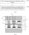
- Step S302 referring to S302 in FIG. 5 and FIG. 7 , the insulating material layer 401 on the sidewall and the bottom of the second part 132 is removed, the remaining insulating material layer 401 on the sidewall of the first part 131 being the insulating layer 14.
- the insulating material layer 401 on the sidewall and the bottom of the second part 132 may be removed with, but not limited to, the dry etching.
- the stacked structure may further be etched with the wet etching to widen the TSV 13, thus fully exposing the pad 114 in each of the first chip 11 and the second chip 12.
- Step S4 referring to S4 in FIG. 2 and FIGS. 8-9 , a conductive layer 15 is formed in the TSV 13.
- the conductive layer 15 is electrically connected to the penetrated metal layer 113 in each of the first chip 11 and the second chip 12.
- Step S4 may further include the following steps:
- steps in the flowcharts of FIG. 2 , FIG. 5 and FIG. 9 are shown in sequence according to the arrows, these steps are unnecessarily executed in the sequence indicated by the arrows.
- the execution order of these steps is not strictly limited, and these steps may be executed in other orders, unless clearly described otherwise.
- at least one of the steps in FIG. 2 , FIG. 5 and FIG. 9 may include a plurality of steps or stages.
- the steps or stages are unnecessarily executed at the same time, but may be executed at different times.
- the execution order of the steps or stages is unnecessarily carried out sequentially, but may be executed alternately with other steps or at least one of the steps or stages of other steps.
- the present application further provides a semiconductor structure, including a stacked structure, a TSV 13, an insulating layer 14 and a conductive layer 15.
- the stacked structure includes a first chip 11 and a second chip 12.
- the second chip 12 is bonded onto the first chip 11 in an F2F manner.
- the first chip 11 and the second chip 12 each include a substrate 111, a dielectric layer 112 on the substrate 111 and a metal layer 113 in the dielectric layer 112.
- the TSV 13 includes a first part 131 and a second part 132 communicating with the first part 131.
- the first part 131 penetrates through the substrate 111 of the second chip 12.
- a sidewall of the first part 131 is a vertical sidewall.
- the second part 132 penetrates through the metal layer 113 of the second chip 12 and at least a part of the metal layer 113 in the first chip 11.
- a sidewall of the second part 132 is an inclined sidewall.
- a bottom of the second part 132 is narrower than a top of the second part 132.
- the insulating layer 14 is located on the sidewall of the first part 131.
- the conductive layer 15 is located in the TSV 13 and fills up the TSV 13. The conductive layer 15 is electrically connected to the penetrated metal layer 113 in each of the first chip 11 and the second chip 12.
- the semiconductor structure in the present application can implement electrical connection between the metal layers in the first chip and the second chip without an additional conductive structure, and thus the semiconductor structure and the process steps can be simplified.
- the semiconductor With the inclined sidewall of the second part, the semiconductor only forms the insulating layer on the sidewall of the first part to simplify the process steps and reduce the cost.
- the substrate 111 may include, but is not limited to, a silicon substrate, a sapphire substrate, a silicon nitride substrate or a silicon oxynitride substrate.
- the dielectric layer 112 may include, but is not limited to, a silicon dioxide layer or a silicon nitride layer. There are no limits made on the material of the substrate 111 and the dielectric layer 112 in the present application.
- the first chip 11 and the second chip 12 each may further include a pad 114.
- the pad 114 may be located at a side of the metal layer 113 away from the substrate 111.
- the pad 114 may include, but is not limited to, a copper pad. There are no limits made on the material of the pad 114 in the present application.
- the TSV 13 further penetrates through the pad 114 in the first chip 11 and the pad 114 in the second chip 12.
- the sidewall of the second part may have an inclination angle of 60-80° with respect to a surface of the substrate, such as 60°, 65, 70°, 75° or 80°.
- the TSV may have a depth of 50-100 ⁇ m, such as 50 ⁇ m, 65 ⁇ m, 80 ⁇ m or 100 ⁇ m.
- the TSV may have a width of 2-10 ⁇ m, such as 2 ⁇ m, 4 ⁇ m, 6 ⁇ m, 8 ⁇ m or 10 ⁇ m.
- the semiconductor structure may further include a bonding layer 16.
- the bonding layer 16 is located between the first chip 11 and the second chip 12, and contacts the dielectric layer 112 of the first chip 11 and the dielectric layer 112 of the second chip 12.
- the bonding layer 16 may include, but is not limited to, an aluminum/copper composite layer. There are no limits made on the material and structure of the bonding layer 16 in the present application.
- the copper metal Due to a high-temperature working environment, the stable performance of the system is restricted by the conventional aluminum wire.
- the copper metal has the advantages of better thermal conductivity, better electrical conductivity and lower thermal expansion coefficient than the aluminum metal, but copper wire bonding is hardly applied to the semiconductors.
- the manufacturing method of a semiconductor structure provided by the above embodiment takes the aluminum/copper composite layer as the bonding layer 16, in which the aluminum metal can provide the desirable bonding, while the copper metal can provide the desirable electrical, mechanical and thermal properties.
- the conductive layer 15 may include a metal barrier layer and a filling conductive layer.
- the metal barrier layer is located on a surface of the insulating layer and on the sidewall and the bottom of the second part.
- the filling conductive layer is located on a surface of the metal barrier layer and fills up the TSV 13.
- the metal barrier layer may include, but is not limited to, a tantalum layer, and a metal barrier layer made of other materials or a stacked structure thereof. There are no limits made on the material and form of the metal barrier layer.
- the insulating layer 14 may include, but is not limited to, a pad oxide layer.
- the pad oxide layer may include, but is not limited to, a silicon dioxide layer or other oxide layers. There are no limits made on the structure and material of the pad oxide layer.
Landscapes
- Internal Circuitry In Semiconductor Integrated Circuit Devices (AREA)
Claims (14)
- Verfahren zum Herstellen einer Halbleiterstruktur, umfassend:Bereitstellen einer gestapelten Struktur, wobei die gestapelte Struktur einen ersten Chip (11) und einen zweiten Chip (12) umfasst, der zweite Chip (12) Face to Face (F2F) auf den ersten Chip (11) gebondet ist und der erste Chip (11) und der zweite Chip (12) jeweils ein Substrat (111), eine dielektrische Schicht (112) auf dem Substrat (111) und eine Metallschicht (113) in der dielektrischen Schicht (112) (S1) umfassen;Bilden einer Silizium-Durchkontaktierung (TSV) (13) in der gestapelten Struktur, wobei die TSV (13) einen ersten Teil (131) und einen zweiten Teil (132) umfasst, der mit dem ersten Teil (131) in Verbindung steht; der erste Teil (131) das Substrat (111) des zweiten Chips (12) durchdringt; eine Seitenwand des ersten Teils (131) eine vertikale Seitenwand ist; der zweite Teil (132) die Metallschicht (113) des zweiten Chips (12) und mindestens einen Teil der Metallschicht (113) in dem ersten Chip (11) durchdringt; eine Seitenwand des zweiten Teils (132) eine schräge Seitenwand ist und eine Unterseite des zweiten Teils (132) schmaler ist als eine Oberseite des zweiten Teils (132) (S2);Bilden einer Isolierschicht (14) auf der Seitenwand des ersten Teils (131) (S3); undBilden einer leitenden Schicht (15) in der TSV (13), wobei die leitende Schicht (15) elektrisch mit der durchdrungenen Metallschicht (113) in jedem des ersten Chips (11) und des zweiten Chips (12) verbunden ist (S4);dadurch gekennzeichnet, dassdas Bilden einer Isolierschicht (14) auf der Seitenwand des ersten Teils (131) (S3) Folgendes umfasst:Bilden einer Isoliermaterialschicht (401) auf einer Seitenwand und einem Boden der TSV (13); undEntfernen der Isoliermaterialschicht (401) an der Seitenwand und dem Boden des zweiten Teils (132) durch Trockenätzen, wobei die verbleibende Isoliermaterialschicht (401) an der Seitenwand des ersten Teils (131) die Isolierschicht (14) ist.
- Herstellungsverfahren nach Anspruch 1, wobei der erste Chip (11) und der zweite Chip (12) ferner jeweils eine Kontaktfläche (114) aufweisen, die Kontaktfläche (114) an einer vom Substrat (111) entfernten Seite der Metallschicht (113) angeordnet ist und die TSV (13) ferner die Kontaktfläche (114) im ersten Chip (11) und die Kontaktfläche (114) im zweiten Chip (12) durchdringt.
- Herstellungsverfahren nach Anspruch 1, wobei die Seitenwand des zweiten Teils (132) einen Neigungswinkel von 60-80° in Bezug auf eine Oberfläche des Substrats (111) aufweist.
- Herstellungsverfahren nach Anspruch 1, wobei die TSV (13) eine Tiefe von 50-100 µm und eine Breite von 2-10 µm aufweist.
- Herstellungsverfahren nach Anspruch 1, wobei das Bereitstellen einer gestapelten Struktur (S1) Folgendes umfasst:Bereitstellen des ersten Chips (11); undBereitstellen des zweiten Chips (12) und Bonden des zweiten Chips (12) Face to Face (F2F) auf den ersten Chip (11); undwobei das Bilden einer TSV (13) in der gestapelten Struktur (S2) Folgendes umfasst:
Ätzen des ersten Chips (11) und des zweiten Chips (12) durch einen Ätzprozess zum Bilden der TSV (13). - Herstellungsverfahren nach Anspruch 5, wobei der zweite Chip (12) durch eine Bonding-Schicht (16) auf den ersten Chip (11) gebondet ist und die TSV (13) ferner die Bonding-Schicht (16) durchdringt.
- Herstellungsverfahren nach einem der Ansprüche 1 bis 6, wobei das Bilden einer leitenden Schicht (15) in der TSV (13) (S4) Folgendes umfasst:Bilden einer Metallsperrschicht auf einer Oberfläche der Isolierschicht (14) und auf der Seitenwand und dem Boden des zweiten Teils (132); undBilden einer leitenden Füllschicht auf einer Oberfläche der Metallsperrschicht, wobei die leitende Füllschicht die TSV (13) auffüllt.
- Halbleiterstruktur, umfassend:eine gestapelte Struktur, wobei die gestapelte Struktur einen ersten Chip (11) und einen zweiten Chip (12) umfasst, der zweite Chip (12) Face to Face (F2F) auf den ersten Chip (11) gebondet ist und der erste Chip (11) und der zweite Chip (12) jeweils ein Substrat (111), eine dielektrische Schicht (112) auf dem Substrat (111) und eine Metallschicht (113) in der dielektrischen Schicht (112) umfassen;eine Silizium-Durchkontaktierung (TSV) (13), wobei die TSV (13) einen ersten Teil (131) und einen zweiten Teil (132) umfasst, der mit dem ersten Teil (131) in Verbindung steht; der erste Teil (131) das Substrat (111) des zweiten Chips (12) durchdringt; eine Seitenwand des ersten Teils (131) eine vertikale Seitenwand ist; der zweite Teil (131) die Metallschicht (113) des zweiten Chips (12) und mindestens einen Teil der Metallschicht (113) in dem ersten Chip (11) durchdringt; eine Seitenwand des zweiten Teils (132) eine schräge Seitenwand ist und eine Unterseite des zweiten Teils (132) schmaler ist als eine Oberseite des zweiten Teils (132);eine Isolierschicht (14), die sich an der Seitenwand des ersten Teils (131) befindet; undeine leitende Schicht (15), die in der TSV (13) angeordnet ist und die TSV (13) auffüllt, wobei die leitende Schicht (15) elektrisch mit der durchdrungenen Metallschicht (113) in jedem des ersten Chips (11) und des zweiten Chips (12) verbunden ist;dadurch gekennzeichnet, dassdie leitende Schicht (15), die die TSV ausfüllt, an der Unterseite des ersten Teils (131) einen Durchmesser hat, der kleiner ist als der Durchmesser der genannten leitenden Schicht an der Oberseite des zweiten Teils (132).
- Halbleiterstruktur nach Anspruch 8, wobei der erste Chip (11) und der zweite Chip (12) ferner jeweils eine Kontaktfläche (114) aufweisen, die Kontaktfläche (114) an einer vom Substrat (111) entfernten Seite der Metallschicht (113) angeordnet ist und die TSV (13) ferner die Kontaktfläche (114) im ersten Chip (11) und die Kontaktfläche (114) im zweiten Chip (12) durchdringt.
- Halbleiterstruktur nach Anspruch 8, wobei die Seitenwand des zweiten Teils (132) einen Neigungswinkel von 60-80° in Bezug auf eine Oberfläche des Substrats (111) aufweist.
- Halbleiterstruktur nach Anspruch 9, wobei die TSV (13) eine Tiefe von 50-100 µm und eine Breite von 2-10 µm aufweist.
- Halbleiterstruktur nach Anspruch 8, wobei die Halbleiterstruktur ferner Folgendes umfasst: eine Bonding-Schicht (16), die sich zwischen dem ersten Chip (11) und dem zweiten Chip (12) befindet und die dielektrische Schicht (112) des ersten Chips (11) und die dielektrische Schicht (112) des zweiten Chips (12) verbindet.
- Halbleiterstruktur nach einem der Ansprüche 8 bis 12, wobei die leitende Schicht (15) Folgendes umfasst:eine Metallsperrschicht, die sich auf einer Oberfläche der Isolierschicht (14) und auf der Seitenwand und dem Boden des zweiten Teils (132) befindet; undeine leitende Füllschicht, die sich auf einer Oberfläche der Metallsperrschicht befindet und die TSV (13) auffüllt.
- Halbleiterstruktur nach Anspruch 13, wobei die Metallsperrschicht eine Tantalschicht umfasst und die Isolierschicht (14) eine Kontaktflächen-Oxidschicht umfasst.
Applications Claiming Priority (2)
| Application Number | Priority Date | Filing Date | Title |
|---|---|---|---|
| CN202110779490.XA CN115602610B (zh) | 2021-07-09 | 2021-07-09 | 半导体结构及其制备方法 |
| PCT/CN2022/076466 WO2023279720A1 (zh) | 2021-07-09 | 2022-02-16 | 半导体结构及其制备方法 |
Publications (3)
| Publication Number | Publication Date |
|---|---|
| EP4207262A1 EP4207262A1 (de) | 2023-07-05 |
| EP4207262A4 EP4207262A4 (de) | 2024-04-10 |
| EP4207262B1 true EP4207262B1 (de) | 2025-04-23 |
Family
ID=84799446
Family Applications (1)
| Application Number | Title | Priority Date | Filing Date |
|---|---|---|---|
| EP22836480.8A Active EP4207262B1 (de) | 2021-07-09 | 2022-02-16 | Halbleiterstruktur und herstellungsverfahren dafür |
Country Status (2)
| Country | Link |
|---|---|
| US (1) | US11569149B1 (de) |
| EP (1) | EP4207262B1 (de) |
Families Citing this family (1)
| Publication number | Priority date | Publication date | Assignee | Title |
|---|---|---|---|---|
| US12119286B2 (en) * | 2021-05-19 | 2024-10-15 | Changxin Memory Technologies, Inc. | Die, memory and method of manufacturing die |
Family Cites Families (9)
| Publication number | Priority date | Publication date | Assignee | Title |
|---|---|---|---|---|
| CN101533811B (zh) | 2008-03-13 | 2010-10-20 | 力成科技股份有限公司 | 具有硅通孔的半导体芯片构造及其堆叠组合 |
| US8399180B2 (en) * | 2010-01-14 | 2013-03-19 | International Business Machines Corporation | Three dimensional integration with through silicon vias having multiple diameters |
| CN108172562A (zh) * | 2012-06-29 | 2018-06-15 | 索尼公司 | 半导体装置、半导体装置的制造方法和电子设备 |
| US9449914B2 (en) * | 2014-07-17 | 2016-09-20 | Taiwan Semiconductor Manufacturing Company, Ltd. | Stacked integrated circuits with redistribution lines |
| US10121812B2 (en) * | 2015-12-29 | 2018-11-06 | Taiwan Semiconductor Manufacturing Co., Ltd. | Stacked substrate structure with inter-tier interconnection |
| CN107316855A (zh) | 2016-04-27 | 2017-11-03 | 中芯国际集成电路制造(上海)有限公司 | 一种半导体器件及其制造方法和电子装置 |
| EP3531445B1 (de) | 2016-09-07 | 2020-06-24 | IMEC vzw | Verfahren zum bonden und verbinden von integrierten schaltungsvorrichtungen |
| US10141391B2 (en) | 2017-02-23 | 2018-11-27 | International Business Machines Corporation | Microstructure modulation for 3D bonded semiconductor containing an embedded resistor structure |
| US10607924B1 (en) * | 2018-11-23 | 2020-03-31 | Nayna Technology Corporation | Semiconductor package structure and method for preparing the same |
-
2022
- 2022-02-16 EP EP22836480.8A patent/EP4207262B1/de active Active
- 2022-05-10 US US17/662,737 patent/US11569149B1/en active Active
Also Published As
| Publication number | Publication date |
|---|---|
| US20230008118A1 (en) | 2023-01-12 |
| US11569149B1 (en) | 2023-01-31 |
| EP4207262A1 (de) | 2023-07-05 |
| EP4207262A4 (de) | 2024-04-10 |
Similar Documents
| Publication | Publication Date | Title |
|---|---|---|
| CN101752270B (zh) | 堆叠集成电路半导体晶粒的形成方法 | |
| TWI746776B (zh) | 半導體元件及其製造方法 | |
| US8674515B2 (en) | 3D integrated circuits structure | |
| US9793192B2 (en) | Formation of through via before contact processing | |
| US8609506B2 (en) | On-chip heat spreader | |
| US9059167B2 (en) | Structure and method for making crack stop for 3D integrated circuits | |
| CN214672598U (zh) | 三维半导体装置结构和三维半导体装置 | |
| KR102576062B1 (ko) | 관통 실리콘 비아를 포함하는 반도체 소자 및 그 제조 방법 | |
| CN102237300B (zh) | 直通基底穿孔结构及其制造方法 | |
| JP2010045371A (ja) | 導電性保護膜を有する貫通電極構造体及びその形成方法 | |
| US9343364B2 (en) | Semiconductor device and method for manufacturing the same | |
| US10607924B1 (en) | Semiconductor package structure and method for preparing the same | |
| EP4207262A1 (de) | Halbleiterstruktur und herstellungsverfahren dafür | |
| CN115602610B (zh) | 半导体结构及其制备方法 | |
| CN222190707U (zh) | 半导体结构 | |
| CN103247569B (zh) | 穿硅导通体的制法及结构 | |
| US20260101792A1 (en) | Method for manufacturing semiconductor stack structure with ultra thin dies | |
| US20250029913A1 (en) | Semiconductor package and method for fabricating the same | |
| US20260123376A1 (en) | Semiconductor structure with tsv and fabricating method of the same | |
| US20240030187A1 (en) | Semiconductor package and method of manufacturing semiconductor package | |
| US20240421140A1 (en) | Semiconductor package and method of manufacturing the semiconductor package | |
| TWI531027B (zh) | 穿矽導通體之製法及結構 | |
| TW202616477A (zh) | 半導體超薄堆疊結構的製造方法 | |
| CN117766494A (zh) | 半导体芯片、晶圆及其制造方法、封装结构及封装方法 | |
| TW202611979A (zh) | 半導體超薄堆疊結構的製造方法 |
Legal Events
| Date | Code | Title | Description |
|---|---|---|---|
| STAA | Information on the status of an ep patent application or granted ep patent |
Free format text: STATUS: THE INTERNATIONAL PUBLICATION HAS BEEN MADE |
|
| PUAI | Public reference made under article 153(3) epc to a published international application that has entered the european phase |
Free format text: ORIGINAL CODE: 0009012 |
|
| STAA | Information on the status of an ep patent application or granted ep patent |
Free format text: STATUS: REQUEST FOR EXAMINATION WAS MADE |
|
| 17P | Request for examination filed |
Effective date: 20230329 |
|
| AK | Designated contracting states |
Kind code of ref document: A1 Designated state(s): AL AT BE BG CH CY CZ DE DK EE ES FI FR GB GR HR HU IE IS IT LI LT LU LV MC MK MT NL NO PL PT RO RS SE SI SK SM TR |
|
| A4 | Supplementary search report drawn up and despatched |
Effective date: 20240312 |
|
| RIC1 | Information provided on ipc code assigned before grant |
Ipc: H01L 25/065 20230101ALI20240305BHEP Ipc: H01L 23/48 20060101ALI20240305BHEP Ipc: H01L 21/60 20060101ALI20240305BHEP Ipc: H01L 21/768 20060101AFI20240305BHEP |
|
| DAV | Request for validation of the european patent (deleted) | ||
| DAX | Request for extension of the european patent (deleted) | ||
| GRAP | Despatch of communication of intention to grant a patent |
Free format text: ORIGINAL CODE: EPIDOSNIGR1 |
|
| STAA | Information on the status of an ep patent application or granted ep patent |
Free format text: STATUS: GRANT OF PATENT IS INTENDED |
|
| INTG | Intention to grant announced |
Effective date: 20241125 |
|
| P01 | Opt-out of the competence of the unified patent court (upc) registered |
Free format text: CASE NUMBER: APP_66604/2024 Effective date: 20241217 |
|
| GRAS | Grant fee paid |
Free format text: ORIGINAL CODE: EPIDOSNIGR3 |
|
| GRAA | (expected) grant |
Free format text: ORIGINAL CODE: 0009210 |
|
| STAA | Information on the status of an ep patent application or granted ep patent |
Free format text: STATUS: THE PATENT HAS BEEN GRANTED |
|
| AK | Designated contracting states |
Kind code of ref document: B1 Designated state(s): AL AT BE BG CH CY CZ DE DK EE ES FI FR GB GR HR HU IE IS IT LI LT LU LV MC MK MT NL NO PL PT RO RS SE SI SK SM TR |
|
| REG | Reference to a national code |
Ref country code: GB Ref legal event code: FG4D |
|
| REG | Reference to a national code |
Ref country code: CH Ref legal event code: EP |
|
| REG | Reference to a national code |
Ref country code: DE Ref legal event code: R096 Ref document number: 602022013699 Country of ref document: DE |
|
| REG | Reference to a national code |
Ref country code: IE Ref legal event code: FG4D |
|
| REG | Reference to a national code |
Ref country code: NL Ref legal event code: MP Effective date: 20250423 |
|
| PG25 | Lapsed in a contracting state [announced via postgrant information from national office to epo] |
Ref country code: NL Free format text: LAPSE BECAUSE OF FAILURE TO SUBMIT A TRANSLATION OF THE DESCRIPTION OR TO PAY THE FEE WITHIN THE PRESCRIBED TIME-LIMIT Effective date: 20250423 |
|
| REG | Reference to a national code |
Ref country code: AT Ref legal event code: MK05 Ref document number: 1788663 Country of ref document: AT Kind code of ref document: T Effective date: 20250423 |
|
| PG25 | Lapsed in a contracting state [announced via postgrant information from national office to epo] |
Ref country code: FI Free format text: LAPSE BECAUSE OF FAILURE TO SUBMIT A TRANSLATION OF THE DESCRIPTION OR TO PAY THE FEE WITHIN THE PRESCRIBED TIME-LIMIT Effective date: 20250423 Ref country code: ES Free format text: LAPSE BECAUSE OF FAILURE TO SUBMIT A TRANSLATION OF THE DESCRIPTION OR TO PAY THE FEE WITHIN THE PRESCRIBED TIME-LIMIT Effective date: 20250423 Ref country code: PT Free format text: LAPSE BECAUSE OF FAILURE TO SUBMIT A TRANSLATION OF THE DESCRIPTION OR TO PAY THE FEE WITHIN THE PRESCRIBED TIME-LIMIT Effective date: 20250825 |
|
| REG | Reference to a national code |
Ref country code: LT Ref legal event code: MG9D |
|
| PG25 | Lapsed in a contracting state [announced via postgrant information from national office to epo] |
Ref country code: GR Free format text: LAPSE BECAUSE OF FAILURE TO SUBMIT A TRANSLATION OF THE DESCRIPTION OR TO PAY THE FEE WITHIN THE PRESCRIBED TIME-LIMIT Effective date: 20250724 Ref country code: NO Free format text: LAPSE BECAUSE OF FAILURE TO SUBMIT A TRANSLATION OF THE DESCRIPTION OR TO PAY THE FEE WITHIN THE PRESCRIBED TIME-LIMIT Effective date: 20250723 |
|
| PG25 | Lapsed in a contracting state [announced via postgrant information from national office to epo] |
Ref country code: PL Free format text: LAPSE BECAUSE OF FAILURE TO SUBMIT A TRANSLATION OF THE DESCRIPTION OR TO PAY THE FEE WITHIN THE PRESCRIBED TIME-LIMIT Effective date: 20250423 |
|
| PG25 | Lapsed in a contracting state [announced via postgrant information from national office to epo] |
Ref country code: BG Free format text: LAPSE BECAUSE OF FAILURE TO SUBMIT A TRANSLATION OF THE DESCRIPTION OR TO PAY THE FEE WITHIN THE PRESCRIBED TIME-LIMIT Effective date: 20250423 |
|
| PG25 | Lapsed in a contracting state [announced via postgrant information from national office to epo] |
Ref country code: HR Free format text: LAPSE BECAUSE OF FAILURE TO SUBMIT A TRANSLATION OF THE DESCRIPTION OR TO PAY THE FEE WITHIN THE PRESCRIBED TIME-LIMIT Effective date: 20250423 |
|
| PG25 | Lapsed in a contracting state [announced via postgrant information from national office to epo] |
Ref country code: AT Free format text: LAPSE BECAUSE OF FAILURE TO SUBMIT A TRANSLATION OF THE DESCRIPTION OR TO PAY THE FEE WITHIN THE PRESCRIBED TIME-LIMIT Effective date: 20250423 |
|
| PG25 | Lapsed in a contracting state [announced via postgrant information from national office to epo] |
Ref country code: RS Free format text: LAPSE BECAUSE OF FAILURE TO SUBMIT A TRANSLATION OF THE DESCRIPTION OR TO PAY THE FEE WITHIN THE PRESCRIBED TIME-LIMIT Effective date: 20250723 |
|
| PG25 | Lapsed in a contracting state [announced via postgrant information from national office to epo] |
Ref country code: IS Free format text: LAPSE BECAUSE OF FAILURE TO SUBMIT A TRANSLATION OF THE DESCRIPTION OR TO PAY THE FEE WITHIN THE PRESCRIBED TIME-LIMIT Effective date: 20250823 |
|
| PG25 | Lapsed in a contracting state [announced via postgrant information from national office to epo] |
Ref country code: LV Free format text: LAPSE BECAUSE OF FAILURE TO SUBMIT A TRANSLATION OF THE DESCRIPTION OR TO PAY THE FEE WITHIN THE PRESCRIBED TIME-LIMIT Effective date: 20250423 |
|
| REG | Reference to a national code |
Ref country code: DE Ref legal event code: R079 Ref document number: 602022013699 Country of ref document: DE Free format text: PREVIOUS MAIN CLASS: H01L0021768000 Ipc: H10W0020000000 |
|
| PG25 | Lapsed in a contracting state [announced via postgrant information from national office to epo] |
Ref country code: DK Free format text: LAPSE BECAUSE OF FAILURE TO SUBMIT A TRANSLATION OF THE DESCRIPTION OR TO PAY THE FEE WITHIN THE PRESCRIBED TIME-LIMIT Effective date: 20250423 Ref country code: SM Free format text: LAPSE BECAUSE OF FAILURE TO SUBMIT A TRANSLATION OF THE DESCRIPTION OR TO PAY THE FEE WITHIN THE PRESCRIBED TIME-LIMIT Effective date: 20250423 |
|
| PG25 | Lapsed in a contracting state [announced via postgrant information from national office to epo] |
Ref country code: CZ Free format text: LAPSE BECAUSE OF FAILURE TO SUBMIT A TRANSLATION OF THE DESCRIPTION OR TO PAY THE FEE WITHIN THE PRESCRIBED TIME-LIMIT Effective date: 20250423 |
|
| PG25 | Lapsed in a contracting state [announced via postgrant information from national office to epo] |
Ref country code: EE Free format text: LAPSE BECAUSE OF FAILURE TO SUBMIT A TRANSLATION OF THE DESCRIPTION OR TO PAY THE FEE WITHIN THE PRESCRIBED TIME-LIMIT Effective date: 20250423 |
|
| REG | Reference to a national code |
Ref country code: DE Ref legal event code: R097 Ref document number: 602022013699 Country of ref document: DE |
|
| PG25 | Lapsed in a contracting state [announced via postgrant information from national office to epo] |
Ref country code: SK Free format text: LAPSE BECAUSE OF FAILURE TO SUBMIT A TRANSLATION OF THE DESCRIPTION OR TO PAY THE FEE WITHIN THE PRESCRIBED TIME-LIMIT Effective date: 20250423 |
|
| PG25 | Lapsed in a contracting state [announced via postgrant information from national office to epo] |
Ref country code: IT Free format text: LAPSE BECAUSE OF FAILURE TO SUBMIT A TRANSLATION OF THE DESCRIPTION OR TO PAY THE FEE WITHIN THE PRESCRIBED TIME-LIMIT Effective date: 20250423 |
|
| PLBE | No opposition filed within time limit |
Free format text: ORIGINAL CODE: 0009261 |
|
| STAA | Information on the status of an ep patent application or granted ep patent |
Free format text: STATUS: NO OPPOSITION FILED WITHIN TIME LIMIT |
|
| REG | Reference to a national code |
Ref country code: CH Ref legal event code: L10 Free format text: ST27 STATUS EVENT CODE: U-0-0-L10-L00 (AS PROVIDED BY THE NATIONAL OFFICE) Effective date: 20260304 |
|
| 26N | No opposition filed |
Effective date: 20260126 |
|
| PGFP | Annual fee paid to national office [announced via postgrant information from national office to epo] |
Ref country code: DE Payment date: 20260218 Year of fee payment: 5 |