EP3270414A1 - Integrated circuit implementing standard cells with metal layer segments extending out of cell boundary - Google Patents
Integrated circuit implementing standard cells with metal layer segments extending out of cell boundary Download PDFInfo
- Publication number
- EP3270414A1 EP3270414A1 EP16205250.0A EP16205250A EP3270414A1 EP 3270414 A1 EP3270414 A1 EP 3270414A1 EP 16205250 A EP16205250 A EP 16205250A EP 3270414 A1 EP3270414 A1 EP 3270414A1
- Authority
- EP
- European Patent Office
- Prior art keywords
- cell
- metal
- edge
- boundary
- segment
- Prior art date
- Legal status (The legal status is an assumption and is not a legal conclusion. Google has not performed a legal analysis and makes no representation as to the accuracy of the status listed.)
- Pending
Links
Images
Classifications
-
- H—ELECTRICITY
- H10—SEMICONDUCTOR DEVICES; ELECTRIC SOLID-STATE DEVICES NOT OTHERWISE PROVIDED FOR
- H10D—INORGANIC ELECTRIC SEMICONDUCTOR DEVICES
- H10D84/00—Integrated devices formed in or on semiconductor substrates that comprise only semiconducting layers, e.g. on Si wafers or on GaAs-on-Si wafers
-
- G—PHYSICS
- G06—COMPUTING OR CALCULATING; COUNTING
- G06F—ELECTRIC DIGITAL DATA PROCESSING
- G06F30/00—Computer-aided design [CAD]
- G06F30/30—Circuit design
- G06F30/39—Circuit design at the physical level
- G06F30/392—Floor-planning or layout, e.g. partitioning or placement
-
- G—PHYSICS
- G06—COMPUTING OR CALCULATING; COUNTING
- G06F—ELECTRIC DIGITAL DATA PROCESSING
- G06F30/00—Computer-aided design [CAD]
- G06F30/30—Circuit design
- G06F30/39—Circuit design at the physical level
- G06F30/394—Routing
-
- H—ELECTRICITY
- H10—SEMICONDUCTOR DEVICES; ELECTRIC SOLID-STATE DEVICES NOT OTHERWISE PROVIDED FOR
- H10D—INORGANIC ELECTRIC SEMICONDUCTOR DEVICES
- H10D89/00—Aspects of integrated devices not covered by groups H10D84/00 - H10D88/00
- H10D89/10—Integrated device layouts
-
- G—PHYSICS
- G06—COMPUTING OR CALCULATING; COUNTING
- G06F—ELECTRIC DIGITAL DATA PROCESSING
- G06F2111/00—Details relating to CAD techniques
- G06F2111/20—Configuration CAD, e.g. designing by assembling or positioning modules selected from libraries of predesigned modules
-
- H—ELECTRICITY
- H10—SEMICONDUCTOR DEVICES; ELECTRIC SOLID-STATE DEVICES NOT OTHERWISE PROVIDED FOR
- H10D—INORGANIC ELECTRIC SEMICONDUCTOR DEVICES
- H10D84/00—Integrated devices formed in or on semiconductor substrates that comprise only semiconducting layers, e.g. on Si wafers or on GaAs-on-Si wafers
- H10D84/90—Masterslice integrated circuits
- H10D84/903—Masterslice integrated circuits comprising field effect technology
- H10D84/907—CMOS gate arrays
- H10D84/968—Macro-architecture
- H10D84/974—Layout specifications, i.e. inner core regions
- H10D84/975—Wiring regions or routing
Definitions
- the present disclosure relates generally to integrated circuit devices and, more particularly, standard-cell based design and fabrication of integrated circuit devices.
- CMOS complementary metal-oxide-semiconductor
- ASICs application-specific integrated circuits
- SoCs Systems-on-a-chip
- IC complex integrated circuit
- a standard cell is a collection of gate-level elements and interconnection structures standardized at a functional level.
- EDA Electronic design automation
- IC integrated circuit
- One such EDA tool is a place and route tool, which builds the physical layout of an IC design from the cells represented by the standard cell library. The place and route tool places the cells side-by-side and uses a routing tool to electrically connect the cells in a specified way to implement corresponding logic of the IC design.
- the semiconductor foundry typically supplies the designer with a set of design rules that apply to a specified technology process, whereby these design rules specify various parameters pertaining to spacing, width, enclosure, and extension for the physical elements within the physical layout of the IC design.
- a design rule check (DRC) tool thus applies the specified design rules to the IC design to verify that all design rules are met and thus the IC may be fabricated as designed using the specified technology process.
- the design and fabrication process of an IC structure using a cell-based methodology typically entails the verification of the physical layout of the IC design in view of various design rules provided by a semiconductor foundry for a specified technology process. These design rules often include a subset of design rules pertaining to the spacing and other interactions between metal segments of abutting or adjacent cells at the Metal 1 (M1) layer.
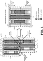
- FIG. 1 illustrates examples of such design rules, and the conventional approach to standard cell design so as to conform with such rules.
- each standard cell represents a corresponding function of the IC design (e.g., a Boolean logic function or a storage function) and is formed of transistor elements and the conductive interconnects that connect the various transistor elements of the cell.
- each cell has a cell boundary containing one or more P-type or N-type active regions formed in a semiconductor substrate or, for a silicon-on-insulator (SOI) implementation, an epitaxial layer of doped or undoped semiconductor material.
- SOI silicon-on-insulator
- One or more metal layers are then formed over the active area and patterned so as to form metal segments at one or more layers, whereby these metal segments serve to interconnect circuit elements within the cell or to interconnect circuit elements between cells.
- Each cell includes a plurality of metal tracks that define the positions and dimensions the metal segments may occupy at a given metal layer.
- the cell 101 includes metal tracks 103, 104, 105, 106 that extend from edge 107 to opposing edge 108 of a cell boundary 110 for the cell 101
- the cell 102 includes, for the M1 layer, metal tracks 111, 112, 113 that extend from edge 114 to opposing edge 115 of a cell boundary 116 for the cell 102.
- metal tracks that are to contain at least one metal segment are filled with metal, and then one or more cut masks (or “trim” masks) are used to pattern the metal within the metal tracks so as to form the intended pattern of metal segments at the given metal layer.
- cut masks also are used to cut the metal at cell boundaries so as to prevent shorts or other undesirable electrical interactions between metal segments of adjacent, or abutting, cells.
- one or more cut masks may introduce metal cuts 117, 118 at the cell boundaries 110, 116 so as to electrically isolate the M1 metal segments of cell 101 from the M1 metal segments of cell 102, and vice versa.
- a semiconductor foundry may supply a set of design rules that includes design rules pertaining to the termination of metal segments in relation to the location of various boundary metal cuts.
- the design rule set may include a tip-to-tip minimum distance requirement that specifies that unless the tips of two metal segments in the same track in abutting cells are immediately adjacent to each other (that is, the metal runs continuously across the abutting cell boundaries), the tips must be a minimum distance apart that typically represents the width of the metal cut layer.
- a metal segment 122 in metal track 104 of cell 101 would trigger a cell boundary design rule violation 124 as the tip of the metal segment 122 terminates in the region of the metal cut 118 while there is no abutting tip of a metal segment in the corresponding metal track 111 of the cell 102.
- the metal segment 126 in metal track 106 of cell 101 and the metal segment 128 in the metal track 113 of cell 102 together would trigger a tip-to-tip minimum distance design rule violation 130 as the facing tips of the metal segments 126, 128 are not separated by a minimum specified distance (given that they are not immediately abutting so that a continuous metal segment is formed across the metal cut 118).
- boundary-related design rules for the M1 layer have resulted in the conventional M1 layer approach for standard cells as exemplarily illustrated by diagram 140 of FIG. 1 .
- conventional standard cell designs resolve the boundary-related design rules by employing an abutment offset zone on each edge of a cell 142 that may abut another cell in the same row (e.g., abutment offset zones 144, 146 at opposing edges 148, 150, respectively, of cell boundary 152).
- a metal segment may either terminate at the cell boundary (e.g., metal segment 154) or terminate short of the abutment offset zone (e.g., metal segments 156, 158), but may not terminate within the abutment offset zone.
- the length of the abutment offset zone is set to approximately half the minimum tip-to-tip spacing required by the design rules.
- the length of the abutment offset zone may be set to approximately 60 nm, and thus when two cells are placed in adjacent locations, the two facing abutment offset zones together provide the 120 nm minimum tip-to-tip spacing.
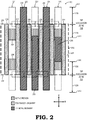
- FIG. 2 illustrates an improved standard cell design approach that conforms to boundary cut design rules and tip-to-tip spacing design rules while also facilitating M1 routing and increased pin access to higher metal layers in accordance with some embodiments.
- a cell 200 includes one or more active regions (e.g., active regions 202, 204), polysilicon segments (e.g., polysilicon segments 206, 207, 208, 209, 210, 211), and other circuit elements formed on a semiconductor substrate 201 (or SOI substrate) and contained within a cell boundary 212, with the cell layout extending in both the orthogonal X and Y directions as shown.
- the cell 200 further includes, at the M1 metal layer, a plurality of metal tracks extending along the Y direction, such as metal tracks 221, 222,223,224,225.
- each metal track either is devoid of metal segments, or contains one or more metal segments that extend within the corresponding metal track.
- the design of cell 200 does not incorporate abutment exclusion zones that require termination of metal tips at either the cell boundary or a minimum distance from the cell boundary. Rather, as shown in the example of FIG. 2 , the design of cell 200 provides that the tip of a M1 metal segment must either (1) terminate at least a specified minimum distance 226 from the corresponding edge of the cell boundary 212, or (2) extend beyond the corresponding edge of the cell boundary 212 by a specified distance 228.
- the design approach for cell 200 is to employ, at each opposing edge 230, 232 of the cell boundary 212, a corresponding tip exclusion zone 234, 236 that extends from within the cell boundary 212 to beyond the cell boundary to a plane that is the specified distance 228 from the corresponding boundary edge.
- a metal segment is specified so as to terminate at or before the in-boundary edge 240, or the metal segment must terminate outside of the cell boundary 212 at the out-of-boundary edge 242.
- the depicted example implementation of cell 200 includes four metal segments: metal segment 252 in track 222, and having a tip terminating at out-of-boundary edge 242 of the tip exclusion zone 234 and a tip terminating at out-of-boundary edge 242 of the tip exclusion zone 236; metal segment 253 in track 223, and having a tip terminating at out-of-boundary edge 242 of the tip exclusion zone 234 and a tip terminating at or before the in-boundary edge 240 of the tip exclusion zone 236; metal segment 254 in track 224, and having a tip terminating at out-of-boundary edge 242 of the tip exclusion zone 234 and a tip terminating at out-of-boundary edge 242 of the tip exclusion zone 236; and metal segment 255 in track 225, and having a tip terminating at or before the in-boundary edge 240 of the tip exclusion zone 234 and a tip terminating at or before the in-boundary edge 240 of the tip exclusion zone 236; metal
- This design approach has a number of advantages. By ensuring that the tip of a metal segment either terminates at least the minimum distance 226 from the cell boundary edge or extends beyond the cell boundary edge by the distance 228, two adjacent cells employing this design approach will result in a physical layout for the two cells in which, for any given metal segment in one cell, the distance between the tip of this metal segment is at least the minimum specified tip-to-tip distance from the facing tip of the metal segment in the corresponding track of the other cell, or the tip of the metal segment of one cell extends into the corresponding track of the other cell, and thus complies with the design rule that specifies that M1 metal must either completely absent from a set of abutting tracks within a metal cut region, or the M1 metal must extend entirely across the metal cut region for the set of abutting tracks.
- the distances 226, 228 are set to be approximately equal, such that a metal segment in one cell that has a tip that terminates at the distance 226 from an edge of the cell boundary of that cell will abut the tip of a metal segment that extends the distance 228 from the corresponding edge of the cell boundary of an adjacent cell, as illustrated in greater detail below.
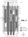
- FIG. 3 illustrates an example of the beneficial implementation of the cell design approach outlined above in accordance with some embodiments.
- an IC structure 300 e.g., an ASIC or system on a chip (SOC)
- the cell 301 comprises circuit elements defined within a cell boundary 304
- the cell 302 likewise comprises circuit elements defined within a cell boundary 306, wherein the cell boundaries 304, 306 abut at boundary edges 308, 310, respectively.
- the cell 301 includes metal tracks 311, 312, 313, 314, 315 at the M1 layer
- the cell 302 includes corresponding metal tracks 321, 322, 323, 324, 325 at the M1 layer.
- the cell 301 includes metal segments 331, 332, 335 in tracks 311, 312, 315, respectively, and metal tracks 313, 314 are unused by the cell 301.
- the cell 302 includes metal segments 342, 343, 344, 345 in tracks 322, 323, 324, 325, respectively, and metal track 321 is unused by the cell 302.
- the cells 301, 302 employ the tip exclusion zones at their opposing row boundaries, as described above. Accordingly, in compliance with this cell design, the metal segment 331 has one tip that terminates within the cell boundary 304 at, or before, the distance 226 ( FIG. 2 ) from the boundary edge 316 (that opposes boundary edge 308) and an opposite tip that extends beyond the cell boundary 304 to the distance 228 ( FIG.
- the metal segment 332 has one tip that that terminates within the cell boundary 304 at, or before, the distance 226 from the boundary edge 308 and an opposite tip that extends beyond the cell boundary 304 to the distance 228 from the boundary edge 316; and the metal segment 335 has opposing tips that terminate within the cell boundary 304 at, or before, the distance 226 from the boundary edges 308, 316, respectively.
- the metal segment 342 has one tip that terminates outside of the cell boundary 306 at the distance 228 from the boundary edge 310 and an opposing tip that terminates outside the cell boundary 306 at the distance 228 from a boundary edge 318 (that opposes boundary edge 310);
- the metal segment 343 has one tip that terminates within the cell boundary 306 at, or before, the distance 226 from the boundary edge 310 and an opposing tip that terminates outside of the cell boundary 306 at the distance 228 from the boundary edge 318;
- the metal segment 344 has one tip that terminates outside of the cell boundary 306 at the distance 228 from the boundary edge 310 and an opposing tip that terminates outside the cell boundary 306 at the distance 228 from the boundary edge 318, and the metal segment 344 has opposing tips that terminate within the cell boundary 306 at, or before, the distance 226 from the boundary edges 310, 316, respectively.
- the metal segment 331 extends from the boundary edge 308 into a portion of the track 321 of the cell 302, and thus complying with the boundary cut design rule that would be applied for a metal cut 350 that would be employed to electrically isolate metal segments of the cells 301, 302 from each other.
- the metal segment 342 extends from cell 302 into the unoccupied region of the metal track 312 of cell 301, thus complying with the boundary cut design rule applied for the metal cut 350.
- the distances 226 and 228 are equal, and thus the out-of-boundary tip of the metal segment 342 abuts or overlaps the facing in-boundary tip of metal segment 332, thereby forming a single metal segment that spans both tracks 312, 322 until the metal cut 350 is performed. Additionally, the metal segment 343 terminates outside of the metal cut 350, and thus complies with the boundary cut design rule.
- the metal segment 344 has a tip that extends from cell 302 into the corresponding track 314 of cell 301, and to an extent that spans the breadth of the metal cut 350, and thus ensuring that the metal segment 344 complies with the boundary cut design rule.
- Metal segments 335, 345 each terminate at least the distance 226 before their respective abutting boundary edges 308, 310.
- the distance 226 is set to be at least one-half of the minimum tip-to-tip distance specified by the design rules
- the spacing between the tip of the metal segment 335 and the facing tip of the metal segment 345 complies with this minimum tip-to-tip spacing.
- the cell design approach outlined above and employed in the example of FIG. 3 facilitates compliance with the boundary-related design rules described above.
- this cell design approach has additional benefits pertaining to inter-cell routing and intra-cell routing.
- other M1 segments (not shown) of the cells 301, 302, respectively may be routed so as to connect to these segments in the unused portions of the metal tracks 315, 325, respectively.
- output pin routing may require corresponding M1 segments to reach one boundary for pin hookup
- the other side of the metal track may be used for M1 stub routing.
- tracks 311, 313, 314, 315, 321, 325 have unused regions 351, 353, 354, 355, 361, 365, respectively, available for M1 stub routing (e.g., metal stub 356 in region 353).
- a benefit of this cell design is that the M1 layer can be used to connect to the cell's M1 pins, as opposed to being forced to use the M2 layer to hook up to the pins. So for example, if one wants to connect segments 335 and 345, one M1 segment can be used to form the connection. In the absence of this design approach, the M1 segment would have been extended and cut on the boundary so the connection would be forced to go up to the M2 layer (horizontal) and then a segment of vertical M3 metal would have connected the two horizontal M2 segments. This adds resistance and capacitance to the pins in addition to blocking precious M2 and M3 routing resources.
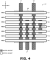
- FIG. 4 depicts an example standard cell 400 for which the M2 layer includes a plurality of M2 metal segments 401, 402, 403, 404, 405, 406, 407 that run horizontally within a cell boundary 408 of the cell 400.
- cell 400 includes metal segments 410, 411, 412, 413 extending along the vertical direction (Y direction) and thus orthogonally intersecting one or more of the M2 metal segments from the perspective of the illustrated plan view of the cell 400.
- metal segments 410-413 adhere to the cell design approach described above, and thus the metal segments 410, 411, 412 extend a set distance beyond the respective edges of the cell boundary 408.
- metal segment 413 terminates at both ends at least the distance 226 before the respective edges of the cell boundary 408, and thus represents a metal segment as typically found in a conventional approach to M1 metal design for a standard cell.
- the metal segment 413 is capable of connecting to only one M2 metal segment (M2 metal segment 404) using a via (e.g., via 414), whereas metal segment 411, by virtue of its extension beyond the bottom edge of the cell boundary 408, can connect to up to three M2 metal segments (M2 metal segments 404, 405, 406) using corresponding vias and metal segments 410, 412, by virtue of their extensions beyond both the top edge and the bottom edge of the cell boundary 408, can connect to up to five M2 metal segments (M2 metal segments 402, 403, 404, 405, 406) using corresponding vias.
- the cell design approach described herein enables an M1 metal segment to run under a greater number of M2 metal segments, and thus facilitates greater M1-M2 routing resources.
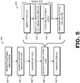
- FIG. 5 is a flow diagram illustrating an example method 500 for the design and fabrication of an ASIC, SoC, or other IC structure implementing one or more aspects in accordance with some embodiments.
- the code generated for each of the following processes is stored or otherwise embodied in non-transitory computer readable storage media for access and use by the corresponding design tool or fabrication tool.
- a functional specification for the IC structure is generated.
- the functional specification (often referred to as a micro architecture specification (MAS)) may be represented by any of a variety of programming languages or modeling languages, including C, C++, SystemC, Simulink, or MATLAB.
- the functional specification is used to generate hardware description code representative of the hardware of the IC structure.
- the hardware description code is represented using at least one Hardware Description Language (HDL), which comprises any of a variety of computer languages, specification languages, or modeling languages for the formal description and design of the circuits of the IC structure.
- HDL Hardware Description Language
- the generated HDL code typically represents the operation of the circuits of the IC structure, the design and organization of the circuits, and tests to verify correct operation of the IC structure through simulation. Examples of HDL include Analog HDL (AHDL), Verilog HDL, SystemVerilog HDL, and VHDL.
- the hardware descriptor code may include register transfer level (RTL) code to provide an abstract representation of the operations of the synchronous digital circuits.
- RTL register transfer level
- the hardware descriptor code may include behavior-level code to provide an abstract representation of the circuitry's operation.
- the HDL model represented by the hardware description code typically is subjected to one or more rounds of simulation and debugging to pass design verification.
- a synthesis tool is used to synthesize the hardware description code to generate code representing or defining an initial physical implementation of the circuitry of the IC structure.
- the synthesis tool generates one or more netlists comprising circuit device instances (e.g., gates, transistors, resistors, capacitors, inductors, diodes, etc.) and the nets, or connections, between the circuit device instances.
- circuit device instances e.g., gates, transistors, resistors, capacitors, inductors, diodes, etc.
- all or a portion of a netlist is generated manually without the use of a synthesis tool.
- the netlists may be subjected to one or more test and verification processes before a final set of one or more netlists is generated.
- a schematic editor tool is used to draft a schematic of circuitry of the IC structure and a schematic capture tool then is used to capture the resulting circuit diagram and to generate one or more netlists (stored on a computer readable media) representing the components and connectivity of the circuit diagram.
- the captured circuit diagram may then be subjected to one or more rounds of simulation for testing and verification.
- one or more EDA tools use the netlists produced at block 506 to generate code representing the physical layout of the circuitry of the IC structure.
- This process includes, for example, a place and route tool using the netlists to determine or fix the location of each element of the circuitry of the IC structure. Further, a routing tool builds on the placement process to add and route the wires needed to connect the circuit elements in accordance with the netlist(s).
- the resulting code represents a three-dimensional model of the IC structure.
- the code is represented in a database file format, such as, for example, the Graphic Database System II (GDSII) format. Data in this format typically represents geometric shapes, text labels, and other information about the circuit layout in hierarchical form.
- GDSII Graphic Database System II
- the physical layout code (e.g., GDSII code) is provided to a semiconductor foundry, which uses the physical layout code to configure or otherwise adapt fabrication tools of the semiconductor foundry (e.g., through mask works) to fabricate the IC structure. That is, the physical layout code is programmed into one or more computer systems, which may then control, in whole or part, the operation of the tools of the manufacturing facility or the manufacturing operations performed therein.
- sub-process 512 illustrates the generation of the physical layout code using a standard cell methodology that employs the tip exclusion zone approach for the M1 layer as described above.
- a place and route tool uses the netlist to identify a function (e.g., logic or storage) to be performed by the represented design and at block 516 the place and route tool accesses one or more standard cell libraries to identify a standard cell corresponding to the identified function.
- the standard cell includes a cell design incorporating the tip exclusion zones.
- the place and route tool identifies a location in a row of the physical layout of the IC design to place the selected standard cell and places the standard cell in this selected location in the physical layout.
- metal segments extending beyond the cell boundary of the standard cell may extend into the empty/unused portions of the corresponding metal tracks of the standard cells abutting the cell on either side in the row, as described above.
- the process of 514-518 then may repeat for each identified function in the netlist or a portion thereof.
- the place and route tool may then perform intra-cell routing within the standard cells and inter-cell routing between the standard cells, wherein the unused portions of the metal tracks having metal segments that extend beyond the cell boundaries is used for M1 stub routing, as described above.
- a computer readable storage medium may include any non-transitory storage medium, or combination of non-transitory storage media, accessible by a computer system during use to provide instructions and/or data to the computer system.
- Such storage media can include, but is not limited to, optical media (e.g., compact disc (CD), digital versatile disc (DVD), Blu-Ray disc), magnetic media (e.g., floppy disc, magnetic tape, or magnetic hard drive), volatile memory (e.g., random access memory (RAM) or cache), non-volatile memory (e.g., read-only memory (ROM) or Flash memory), or microelectromechanical systems (MEMS)-based storage media.
- optical media e.g., compact disc (CD), digital versatile disc (DVD), Blu-Ray disc
- magnetic media e.g., floppy disc, magnetic tape, or magnetic hard drive
- volatile memory e.g., random access memory (RAM) or cache
- non-volatile memory e.g., read-only memory (ROM) or Flash
- the computer readable storage medium is embedded in the computing system (e.g., system RAM or ROM), fixedly attached to the computing system (e.g., a magnetic hard drive), removably attached to the computing system (e.g., an optical disc or Universal Serial Bus (USB)-based Flash memory), or coupled to the computer system via a wired or wireless network (e.g., network accessible storage (NAS)).
- system RAM or ROM system RAM or ROM
- USB Universal Serial Bus
- NAS network accessible storage
- certain aspects of the techniques described above may implemented by one or more processors of a processing system executing software.
- the software comprises one or more sets of executable instructions stored or otherwise tangibly embodied on a non-transitory computer readable storage medium.
- the software can include the instructions and certain data that, when executed by the one or more processors, manipulate the one or more processors to perform one or more aspects of the techniques described above.
- the non-transitory computer readable storage medium can include, for example, a magnetic or optical disk storage device, solid state storage devices such as Flash memory, a cache, random access memory (RAM) or other non-volatile memory device or devices, and the like.
- the executable instructions stored on the non-transitory computer readable storage medium is in source code, assembly language code, object code, or other instruction format that is interpreted or otherwise executable by one or more processors.
Landscapes
- Engineering & Computer Science (AREA)
- Computer Hardware Design (AREA)
- Physics & Mathematics (AREA)
- Theoretical Computer Science (AREA)
- General Engineering & Computer Science (AREA)
- Evolutionary Computation (AREA)
- Geometry (AREA)
- General Physics & Mathematics (AREA)
- Computer Networks & Wireless Communication (AREA)
- Architecture (AREA)
- Design And Manufacture Of Integrated Circuits (AREA)
- Semiconductor Integrated Circuits (AREA)
Priority Applications (3)
| Application Number | Priority Date | Filing Date | Title |
|---|---|---|---|
| KR1020197003688A KR102294210B1 (ko) | 2016-07-12 | 2017-07-10 | 전지 경계로부터 연장되는 금속층 부분을 가진 표준 전지를 구현하는 집적 회로 |
| PCT/US2017/041349 WO2018013472A1 (en) | 2016-07-12 | 2017-07-10 | Integrated circuit implementing standard cells with metal layer segments extending out of cell boundary |
| CN201780043776.3A CN109791930B (zh) | 2016-07-12 | 2017-07-10 | 实现具有延伸出单元边界的金属层段的标准单元的集成电路 |
Applications Claiming Priority (1)
| Application Number | Priority Date | Filing Date | Title |
|---|---|---|---|
| US15/207,691 US9977854B2 (en) | 2016-07-12 | 2016-07-12 | Integrated circuit implementing standard cells with metal layer segments extending out of cell boundary |
Publications (1)
| Publication Number | Publication Date |
|---|---|
| EP3270414A1 true EP3270414A1 (en) | 2018-01-17 |
Family
ID=57890630
Family Applications (1)
| Application Number | Title | Priority Date | Filing Date |
|---|---|---|---|
| EP16205250.0A Pending EP3270414A1 (en) | 2016-07-12 | 2016-12-20 | Integrated circuit implementing standard cells with metal layer segments extending out of cell boundary |
Country Status (7)
| Country | Link |
|---|---|
| US (1) | US9977854B2 (enExample) |
| EP (1) | EP3270414A1 (enExample) |
| JP (1) | JP7015824B2 (enExample) |
| KR (1) | KR102294210B1 (enExample) |
| CN (1) | CN109791930B (enExample) |
| TW (1) | TWI732900B (enExample) |
| WO (1) | WO2018013472A1 (enExample) |
Cited By (1)
| Publication number | Priority date | Publication date | Assignee | Title |
|---|---|---|---|---|
| CN111241769A (zh) * | 2018-11-09 | 2020-06-05 | 三星电子株式会社 | 包括不同类型单元的集成电路及其设计方法和系统 |
Families Citing this family (17)
| Publication number | Priority date | Publication date | Assignee | Title |
|---|---|---|---|---|
| KR102458446B1 (ko) * | 2016-03-03 | 2022-10-26 | 삼성전자주식회사 | 스탠다드 셀을 포함하는 반도체 장치 및 그것의 전자 설계 자동화 방법 |
| US10691849B2 (en) * | 2017-09-28 | 2020-06-23 | Taiwan Semiconductor Manufacturing Co., Ltd. | Metal cut optimization for standard cells |
| DE102018122541A1 (de) | 2017-09-29 | 2019-04-04 | Taiwan Semiconductor Manufacturing Co., Ltd. | Stiftmodifizierung für standardzellen |
| US10559558B2 (en) * | 2017-09-29 | 2020-02-11 | Taiwan Semiconductor Manufacturing Co., Ltd. | Pin modification for standard cells |
| TWI681309B (zh) * | 2018-05-10 | 2020-01-01 | 瑞昱半導體股份有限公司 | 電子裝置測試資料庫產生方法 |
| US10784869B2 (en) * | 2018-07-16 | 2020-09-22 | Taiwan Semiconductor Manufacturing Company, Ltd. | Integrated circuit and method of manufacturing the same |
| DE102019125900B4 (de) | 2018-09-28 | 2022-03-24 | Taiwan Semiconductor Manufacturing Co., Ltd. | Metallschnittgebiet-positionierungsverfahren und system |
| US10997348B2 (en) | 2018-09-28 | 2021-05-04 | Taiwan Semiconductor Manufacturing Company Ltd. | Metal cut region location method and system |
| US10769342B2 (en) * | 2018-10-31 | 2020-09-08 | Taiwan Semiconductor Manufacturing Company Ltd. | Pin access hybrid cell height design |
| US11011417B2 (en) | 2019-05-31 | 2021-05-18 | International Business Machines Corporation | Method and structure of metal cut |
| US10909297B1 (en) * | 2019-08-15 | 2021-02-02 | Taiwan Semiconductor Manufacturing Company Limited | Deterministic system for device layout optimization |
| EP4073677A1 (en) * | 2019-12-09 | 2022-10-19 | Synopsys, Inc. | Electrical circuit design using cells with metal lines |
| CN111931450B (zh) * | 2020-08-11 | 2024-09-20 | 上海华力微电子有限公司 | 一种集成电路数字后端设计的方法和系统 |
| US11290109B1 (en) * | 2020-09-23 | 2022-03-29 | Qualcomm Incorporated | Multibit multi-height cell to improve pin accessibility |
| CN115117052A (zh) | 2021-03-18 | 2022-09-27 | 三星电子株式会社 | 提供增加的引脚接入点的集成电路及其设计方法 |
| KR20230025244A (ko) | 2021-08-13 | 2023-02-21 | 삼성전자주식회사 | 표준 셀을 포함하는 집적 회로 및 이를 설계하기 위한 방법 |
| CN118551721B (zh) * | 2024-07-30 | 2024-10-18 | 上海聪链信息科技有限公司 | N12设计中的防违例绕线方法、装置、设备及存储介质 |
Citations (8)
| Publication number | Priority date | Publication date | Assignee | Title |
|---|---|---|---|---|
| US6174742B1 (en) * | 1998-10-30 | 2001-01-16 | Lsi Logic Corporation | Off-grid metal layer utilization |
| US20100115484A1 (en) * | 2008-11-03 | 2010-05-06 | Arm Limited | Standard cell placement |
| US20120249182A1 (en) * | 2011-03-30 | 2012-10-04 | Synopsys, Inc. | Power Routing in Standard Cell Designs |
| US20130181297A1 (en) * | 2012-01-12 | 2013-07-18 | Taiwan Semiconductor Manufacturing Company, Ltd. | SRAM Cells and Arrays |
| US20140167117A1 (en) * | 2009-10-13 | 2014-06-19 | Tela Innovations, Inc. | Methods for Cell Boundary Encroachment and Layouts Implementing the Same |
| US20140327050A1 (en) * | 2013-05-02 | 2014-11-06 | Taiwan Semiconductor Manufacturing Company, Ltd. | Standard cell having cell height being non-integral multiple of nominal minimum pitch |
| US20150333008A1 (en) * | 2014-05-15 | 2015-11-19 | Qualcomm Incorporated | Standard cell architecture with m1 layer unidirectional routing |
| US20160163714A1 (en) * | 2014-12-03 | 2016-06-09 | Qualcomm Incorporated | Static random access memory (sram) bit cells with wordline landing pads split across boundary edges of the sram bit cells |
Family Cites Families (22)
| Publication number | Priority date | Publication date | Assignee | Title |
|---|---|---|---|---|
| JPH04216668A (ja) * | 1990-12-15 | 1992-08-06 | Sharp Corp | 半導体集積回路 |
| US7036103B2 (en) * | 1999-10-14 | 2006-04-25 | Synopsys, Inc. | Detailed placer for optimizing high density cell placement in a linear runtime |
| US6351841B1 (en) | 2000-03-21 | 2002-02-26 | Cadence Design Systems, Inc. | Method and apparatus for creating multi-gate transistors with integrated circuit polygon compactors |
| US7089521B2 (en) * | 2004-01-27 | 2006-08-08 | International Business Machines Corporation | Method for legalizing the placement of cells in an integrated circuit layout |
| US6903389B1 (en) | 2004-06-15 | 2005-06-07 | Taiwan Semiconductor Manufacturing Company, Ltd. | Variable layout design for multiple voltage applications |
| US7194717B2 (en) * | 2004-09-08 | 2007-03-20 | Lsi Logic Corporation | Compact custom layout for RRAM column controller |
| JP4796817B2 (ja) | 2005-10-31 | 2011-10-19 | エルピーダメモリ株式会社 | 基本セル設計方法、レイアウト設計方法、設計装置およびプログラム |
| US7640522B2 (en) * | 2006-01-14 | 2009-12-29 | Tela Innovations, Inc. | Method and system for placing layout objects in a standard-cell layout |
| US7908578B2 (en) | 2007-08-02 | 2011-03-15 | Tela Innovations, Inc. | Methods for designing semiconductor device with dynamic array section |
| US7564077B2 (en) * | 2006-05-05 | 2009-07-21 | Texas Instruments Incorporated | Performance and area scalable cell architecture technology |
| KR101761530B1 (ko) * | 2008-07-16 | 2017-07-25 | 텔라 이노베이션스, 인코포레이티드 | 동적 어레이 아키텍쳐에서의 셀 페이징과 배치를 위한 방법 및 그 구현 |
| US7919792B2 (en) | 2008-12-18 | 2011-04-05 | Taiwan Semiconductor Manufacturing Company, Ltd. | Standard cell architecture and methods with variable design rules |
| JP5325162B2 (ja) * | 2010-05-18 | 2013-10-23 | パナソニック株式会社 | 半導体装置 |
| US8423946B1 (en) * | 2010-05-25 | 2013-04-16 | Marvell International Ltd. | Circuitry having programmable power rails, architectures, apparatuses, and systems including the same, and methods and algorithms for programming and/or configuring power rails in an integrated circuit |
| US8431968B2 (en) | 2010-07-28 | 2013-04-30 | Taiwan Semiconductor Manufacturing Co., Ltd. | Electromigration resistant standard cell device |
| US8742464B2 (en) | 2011-03-03 | 2014-06-03 | Synopsys, Inc. | Power routing in standard cells |
| US8612914B2 (en) * | 2011-03-23 | 2013-12-17 | Synopsys, Inc. | Pin routing in standard cells |
| US8451026B2 (en) * | 2011-05-13 | 2013-05-28 | Arm Limited | Integrated circuit, method of generating a layout of an integrated circuit using standard cells, and a standard cell library providing such standard cells |
| CN104134657B (zh) * | 2013-05-02 | 2018-01-26 | 台湾积体电路制造股份有限公司 | 单元高度为标称最小间距的非整数倍的标准单元 |
| KR102152772B1 (ko) * | 2013-11-18 | 2020-09-08 | 삼성전자 주식회사 | 레이아웃 디자인 시스템, 레이아웃 디자인 방법, 및 이를 이용하여 제조된 반도체 장치 |
| US9727685B2 (en) * | 2015-05-14 | 2017-08-08 | Globalfoundries Inc. | Method, apparatus, and system for improved standard cell design and routing for improving standard cell routability |
| KR102504289B1 (ko) * | 2016-04-07 | 2023-02-28 | 삼성전자 주식회사 | 인접 핀들 사이의 라우팅 간섭을 제거하는 구조를 갖는 표준 셀과 이를 포함하는 장치 |
-
2016
- 2016-07-12 US US15/207,691 patent/US9977854B2/en active Active
- 2016-12-20 EP EP16205250.0A patent/EP3270414A1/en active Pending
-
2017
- 2017-07-10 CN CN201780043776.3A patent/CN109791930B/zh active Active
- 2017-07-10 WO PCT/US2017/041349 patent/WO2018013472A1/en not_active Ceased
- 2017-07-10 JP JP2019500874A patent/JP7015824B2/ja active Active
- 2017-07-10 KR KR1020197003688A patent/KR102294210B1/ko active Active
- 2017-07-12 TW TW106123326A patent/TWI732900B/zh active
Patent Citations (8)
| Publication number | Priority date | Publication date | Assignee | Title |
|---|---|---|---|---|
| US6174742B1 (en) * | 1998-10-30 | 2001-01-16 | Lsi Logic Corporation | Off-grid metal layer utilization |
| US20100115484A1 (en) * | 2008-11-03 | 2010-05-06 | Arm Limited | Standard cell placement |
| US20140167117A1 (en) * | 2009-10-13 | 2014-06-19 | Tela Innovations, Inc. | Methods for Cell Boundary Encroachment and Layouts Implementing the Same |
| US20120249182A1 (en) * | 2011-03-30 | 2012-10-04 | Synopsys, Inc. | Power Routing in Standard Cell Designs |
| US20130181297A1 (en) * | 2012-01-12 | 2013-07-18 | Taiwan Semiconductor Manufacturing Company, Ltd. | SRAM Cells and Arrays |
| US20140327050A1 (en) * | 2013-05-02 | 2014-11-06 | Taiwan Semiconductor Manufacturing Company, Ltd. | Standard cell having cell height being non-integral multiple of nominal minimum pitch |
| US20150333008A1 (en) * | 2014-05-15 | 2015-11-19 | Qualcomm Incorporated | Standard cell architecture with m1 layer unidirectional routing |
| US20160163714A1 (en) * | 2014-12-03 | 2016-06-09 | Qualcomm Incorporated | Static random access memory (sram) bit cells with wordline landing pads split across boundary edges of the sram bit cells |
Cited By (1)
| Publication number | Priority date | Publication date | Assignee | Title |
|---|---|---|---|---|
| CN111241769A (zh) * | 2018-11-09 | 2020-06-05 | 三星电子株式会社 | 包括不同类型单元的集成电路及其设计方法和系统 |
Also Published As
| Publication number | Publication date |
|---|---|
| CN109791930A (zh) | 2019-05-21 |
| US20180018419A1 (en) | 2018-01-18 |
| JP7015824B2 (ja) | 2022-02-03 |
| KR102294210B1 (ko) | 2021-08-27 |
| JP2019526170A (ja) | 2019-09-12 |
| WO2018013472A1 (en) | 2018-01-18 |
| TW201813050A (zh) | 2018-04-01 |
| US9977854B2 (en) | 2018-05-22 |
| KR20190018542A (ko) | 2019-02-22 |
| TWI732900B (zh) | 2021-07-11 |
| CN109791930B (zh) | 2021-08-27 |
Similar Documents
| Publication | Publication Date | Title |
|---|---|---|
| US9977854B2 (en) | Integrated circuit implementing standard cells with metal layer segments extending out of cell boundary | |
| US9330219B2 (en) | Integrated circuit design method | |
| US11031385B2 (en) | Standard cell for removing routing interference between adjacent pins and device including the same | |
| US9852253B2 (en) | Automated layout for integrated circuits with nonstandard cells | |
| CN107066681B (zh) | 集成电路和制造集成电路的计算机实现方法 | |
| US9928337B2 (en) | Integrated circuit and design method for same | |
| Choi et al. | Probe3. 0: A systematic framework for design-technology pathfinding with improved design enablement | |
| US8234612B2 (en) | Cone-aware spare cell placement using hypergraph connectivity analysis | |
| US12032896B2 (en) | Generation of layout including power delivery network | |
| US20180144083A1 (en) | Method for legalizing mixed-cell height standard cells of ic | |
| TWI789911B (zh) | 用於電容值提取的系統、方法及儲存媒體 | |
| EP4073677A1 (en) | Electrical circuit design using cells with metal lines | |
| US9064081B1 (en) | Generating database for cells routable in pin layer | |
| KR102717096B1 (ko) | 집적 회로 및 상기 집적 회로의 제조를 위한 컴퓨터 구현 방법 | |
| US8966429B2 (en) | Bit slice elements utilizing through device routing | |
| US20170061063A1 (en) | Integrated circuit with reduced routing congestion | |
| US9293450B2 (en) | Synthesis of complex cells | |
| US20040003363A1 (en) | Integrated circuit design and manufacture utilizing layers having a predetermined layout | |
| US12009260B2 (en) | Method and system of forming integrated circuit | |
| Lienig et al. | Methodologies for Physical Design: Models, Styles, Tasks, and Flows | |
| Rakib et al. | Implementing Yosys & OpenROAD for Physical Design (PD) of an IoT Device for Vehicle Detection via ASAP7 PDK. | |
| US20240086609A1 (en) | Integrated circuit design method, system and computer program product | |
| JP2004318716A (ja) | 半導体装置の配置配線方法 |
Legal Events
| Date | Code | Title | Description |
|---|---|---|---|
| PUAI | Public reference made under article 153(3) epc to a published international application that has entered the european phase |
Free format text: ORIGINAL CODE: 0009012 |
|
| STAA | Information on the status of an ep patent application or granted ep patent |
Free format text: STATUS: REQUEST FOR EXAMINATION WAS MADE |
|
| STAA | Information on the status of an ep patent application or granted ep patent |
Free format text: STATUS: EXAMINATION IS IN PROGRESS |
|
| 17P | Request for examination filed |
Effective date: 20161220 |
|
| AK | Designated contracting states |
Kind code of ref document: A1 Designated state(s): AL AT BE BG CH CY CZ DE DK EE ES FI FR GB GR HR HU IE IS IT LI LT LU LV MC MK MT NL NO PL PT RO RS SE SI SK SM TR |
|
| AX | Request for extension of the european patent |
Extension state: BA ME |
|
| 17Q | First examination report despatched |
Effective date: 20171220 |
|
| RAP1 | Party data changed (applicant data changed or rights of an application transferred) |
Owner name: ADVANCED MICRO DEVICES, INC. Owner name: ATI TECHNOLOGIES ULC |
|
| RAP1 | Party data changed (applicant data changed or rights of an application transferred) |
Owner name: ADVANCED MICRO DEVICES, INC. Owner name: ATI TECHNOLOGIES ULC |