EP3205008B1 - Gemeinsam verwendeter bootstrap-kondensator für mehrphasige abwärtswandlerschaltung und verfahren - Google Patents
Gemeinsam verwendeter bootstrap-kondensator für mehrphasige abwärtswandlerschaltung und verfahren Download PDFInfo
- Publication number
- EP3205008B1 EP3205008B1 EP15831490.6A EP15831490A EP3205008B1 EP 3205008 B1 EP3205008 B1 EP 3205008B1 EP 15831490 A EP15831490 A EP 15831490A EP 3205008 B1 EP3205008 B1 EP 3205008B1
- Authority
- EP
- European Patent Office
- Prior art keywords
- bootstrap capacitor
- high side
- coupled
- voltage
- switching
- Prior art date
- Legal status (The legal status is an assumption and is not a legal conclusion. Google has not performed a legal analysis and makes no representation as to the accuracy of the status listed.)
- Active
Links
Images


Classifications
-
- H—ELECTRICITY
- H02—GENERATION; CONVERSION OR DISTRIBUTION OF ELECTRIC POWER
- H02M—APPARATUS FOR CONVERSION BETWEEN AC AND AC, BETWEEN AC AND DC, OR BETWEEN DC AND DC, AND FOR USE WITH MAINS OR SIMILAR POWER SUPPLY SYSTEMS; CONVERSION OF DC OR AC INPUT POWER INTO SURGE OUTPUT POWER; CONTROL OR REGULATION THEREOF
- H02M1/00—Details of apparatus for conversion
- H02M1/08—Circuits specially adapted for the generation of control voltages for semiconductor devices incorporated in static converters
- H02M1/084—Circuits specially adapted for the generation of control voltages for semiconductor devices incorporated in static converters using a control circuit common to several phases of a multi-phase system
-
- H—ELECTRICITY
- H02—GENERATION; CONVERSION OR DISTRIBUTION OF ELECTRIC POWER
- H02M—APPARATUS FOR CONVERSION BETWEEN AC AND AC, BETWEEN AC AND DC, OR BETWEEN DC AND DC, AND FOR USE WITH MAINS OR SIMILAR POWER SUPPLY SYSTEMS; CONVERSION OF DC OR AC INPUT POWER INTO SURGE OUTPUT POWER; CONTROL OR REGULATION THEREOF
- H02M3/00—Conversion of DC power input into DC power output
- H02M3/02—Conversion of DC power input into DC power output without intermediate conversion into AC
- H02M3/04—Conversion of DC power input into DC power output without intermediate conversion into AC by static converters
- H02M3/10—Conversion of DC power input into DC power output without intermediate conversion into AC by static converters using discharge tubes with control electrode or semiconductor devices with control electrode
- H02M3/145—Conversion of DC power input into DC power output without intermediate conversion into AC by static converters using discharge tubes with control electrode or semiconductor devices with control electrode using devices of a triode or transistor type requiring continuous application of a control signal
- H02M3/155—Conversion of DC power input into DC power output without intermediate conversion into AC by static converters using discharge tubes with control electrode or semiconductor devices with control electrode using devices of a triode or transistor type requiring continuous application of a control signal using semiconductor devices only
- H02M3/156—Conversion of DC power input into DC power output without intermediate conversion into AC by static converters using discharge tubes with control electrode or semiconductor devices with control electrode using devices of a triode or transistor type requiring continuous application of a control signal using semiconductor devices only with automatic control of output voltage or current, e.g. switching regulators
- H02M3/158—Conversion of DC power input into DC power output without intermediate conversion into AC by static converters using discharge tubes with control electrode or semiconductor devices with control electrode using devices of a triode or transistor type requiring continuous application of a control signal using semiconductor devices only with automatic control of output voltage or current, e.g. switching regulators including plural semiconductor devices as final control devices for a single load
- H02M3/1584—Conversion of DC power input into DC power output without intermediate conversion into AC by static converters using discharge tubes with control electrode or semiconductor devices with control electrode using devices of a triode or transistor type requiring continuous application of a control signal using semiconductor devices only with automatic control of output voltage or current, e.g. switching regulators including plural semiconductor devices as final control devices for a single load with a plurality of power processing stages connected in parallel
- H02M3/1586—Conversion of DC power input into DC power output without intermediate conversion into AC by static converters using discharge tubes with control electrode or semiconductor devices with control electrode using devices of a triode or transistor type requiring continuous application of a control signal using semiconductor devices only with automatic control of output voltage or current, e.g. switching regulators including plural semiconductor devices as final control devices for a single load with a plurality of power processing stages connected in parallel switched with a phase shift, i.e. interleaved
-
- H—ELECTRICITY
- H03—ELECTRONIC CIRCUITRY
- H03K—PULSE TECHNIQUE
- H03K17/00—Electronic switching or gating, i.e. not by contact-making and –breaking
Definitions
- This relates generally to multiple phase switching circuits in a DC-DC switching converter for providing a stepped down voltage from an input voltage.
- a supply voltage is sometimes provided by an AC to DC transformer, or a "brick", which outputs a DC voltage (such as 12 or 24 volts) when AC power is available.
- Portable devices often also operate on similar DC voltages provided from rechargeable or other batteries when AC power is not available. Some portable devices may not have a "brick", but operate only from batteries.
- Electronics used within the portable devices typically include integrated circuits, such as a microprocessor, volatile or nonvolatile storage devices, digital radio or cellphone transceiver devices, and other functions such as Bluetooth, WiFi, and display drivers.
- the integrated circuit devices are increasingly designed to operate at lower and lower operating voltages, such as 1.8 volts DC or even lower.
- Switching power converter circuits are increasingly useful to provide the DC voltage and current for electronic devices.
- pulse width modulated (“PWM”) converters in a “buck” configuration are often used. These PWM converter circuits are far more efficient and run cooler than the linear regulators used previously to provide the stepped down DC-DC voltage.
- a high side switch such as a MOS transistor
- a pulse width modulated signal coupled to a gate terminal of the high side switch is useful to turn on or "close” the high side switch in an “on” state, and the pulse width modulated signal is useful to turn off or "open” the high side switch in an “off” state.
- the "duty cycle” of the converter is a ratio of the "on” time of the high side switch to the "off” time.
- An inductor is coupled between the switching node and an output terminal for the output voltage.
- An output capacitor is coupled between the output terminal and a ground terminal.
- the rectifying device is useful to supply current into the inductor when the high side switch is open, which is the "off time" for the circuit. Increasingly, this rectifying device is replaced by a low side driver switch, although diode rectifiers are sometimes used.
- a synchronous switching converter topology is created by using a MOSFET transistor for both the high side switch and the low side switch (replacing the older diode rectifier). By using MOSFET transistors with low RDSon values, and by controlling the on and off times for the high side and low side switches, efficient DC-DC buck converter circuits are implemented.
- the DC output voltage obtained at the output terminal is directly proportional to the input DC voltage at the voltage input terminal. More specifically, the output voltage is proportional to the input voltage multiplied by the ratio of the high side switch on-time to the off-time. Accordingly, the DC output voltage is proportional to the duty cycle.
- the pulse width of the "on" state the output voltage may be varied to a desired value, and it may be regulated.
- An onboard or off board oscillator is typically used for obtaining a pulse source that clocks the circuit.
- the output voltage can then be regulated to a desired value by varying the width of the modulated pulse that closes the high side switch, thereby coupling the input voltage or a supply voltage to the switching node for the inductor.
- Additional circuitry is sometimes used for regulating the output during times when no current or low current is flowing into the load.
- the circuit may switch to a pulsed frequency mode or otherwise skip cycles when light load conditions are present.
- U.S. Patent No. 8,710,816, issued April 29, 2014 entitled “Buck Converter having Reduced Ripple under Light Load", to Miyazaki, discloses circuitry for increasing the efficiency of a buck converter circuit when operating under light load.
- buck converter While the buck converter is substantially more efficient than the previously used linear regulators to provide DC voltages, multiple phase buck converters are increasingly used in further improving buck converter performance.
- a multiple phase buck converter several switching circuit stages and corresponding inductors are coupled in parallel to one another, and these multiple stages are operated in non-overlapping phases. The multiple phase outputs are then simply added to form the overall output. Two, three, four or more phases and corresponding circuit stages may exist.
- the addition of the multiple phases increases the complexity of the control circuitry, so a design trade-off exists between the number of phases and the amount (and complexity) of the control circuitry.
- Multiphase buck converters are therefore increasingly used, particularly for supplying DC voltages in microprocessor systems.
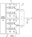
- FIG. 1 is a block diagram of a typical multiphase buck converter circuit 10.
- a first stage switching circuit 11 includes a high side MOSFET switch 111, which is an n-type MOSFET ("NMOS") transistor that is sufficiently large to provide the required or expected load current to the corresponding inductor L_1 during the "on" state.
- a high side driver circuit 113 is coupled to the gate terminal of the MOSFET switch 111.
- the high side MOSFET switch 111 is coupled to switching node SW1, which is coupled to one terminal of inductor L_1.
- a low side switch 117 which in this example is also an N type MOSFET device 117, is coupled between the switch node SW1 and a ground terminal.
- Low side driver 115 controls low side switch 117 by controlling the voltage on the gate terminal of the low side switch 117.
- the low side switch 117 provides a current path to supply current to the inductor L_1.
- the multiphase buck converter 10 has n phases, as indicated by the asterisks. In this example, two phases are shown. However, in practical systems, n can be any positive integer greater than or equal to two, and three and four and more phase buck converter systems are known for various applications. This is indicated in FIG. 1 by the asterisks in the column between the first stage inductor L_1 and the inductor for the bottom stage, labeled L_N.
- the second stage switching circuit 13 is coupled in parallel to the first stage switching circuit 11.
- the circuit elements within second stage switching circuit 13 are duplicated from first stage switching circuit 11 and include a high side MOS switch 131, which again can be an NMOS transistor, a high side driver circuit 133 coupled to the gate terminal of the high side MOS switch 131, and a low side driver circuit 135 coupled to the gate terminal of the low side switch 137.
- the switching circuit 13 is coupled to a switching node SWN, which is coupled to one terminal of the inductor L_N.
- Driver control circuit 15 in FIG. 1 provides the control of the high side driver circuits 113 and 133, and of low side driver circuits 115 and 135.
- the high side MOS switch 111 is closed by driving a gate voltage onto the gate terminal from the high side driver circuit 113 that exceeds the source voltage by a transistor threshold voltage Vt for the high side MOS switch (transistor) 111.
- This action "closes” the high side MOS switch 111 and couples the input voltage Vin to the switching node SW1.
- Current flows into the inductor L_1 and out to the output node, thereby charging capacitor CO, and the load current flows forming an output voltage at the output Vo.
- inductor L_1 stores energy in a magnetic field surrounding the inductor.
- the driver control circuit 15 controls the high side driver circuit 113 and turns off the high side MOSFET switch 111, and the driver control circuit 15 controls low side driver circuit 115 and turns on the low side switch (MOSFET) 117.
- the low side switch 117 provides a current path during the "off” state of the first stage switching circuit 11, so that current flows through the inductor L_1 from the stored energy and into the capacitor CO and into the load (not shown) at the output terminal Vo, which supports the voltage at the output terminal Vo during the "off' state.
- the second stage switching circuit 13 is operated in the same manner as the first stage switching circuit 11, but the two stages are operated in non-overlapping phases. In this manner, the output current provided by the two phase switching circuits 11 and 13 is added at the output Vo, and together the two switching circuits 11 and 13 provide the current to the load.
- Driver control circuit 15 provides the pulses needed to turn on the high side driver circuits 113 and 133 for the high side MOS switches 111 and 131, and to turn on the low side switches 117 and 137, in non-overlapping phases.
- a voltage at the gate terminal of the MOS transistors is needed higher than the input voltage.
- Tthis gate voltage has been formed using a bootstrap capacitor.
- this capacitor is referred to as a "fly cap”, but this disclosure uses the term "bootstrap capacitor".
- the bootstrap capacitor is first configured with a top plate coupled to a positive supply voltage, such as an internally regulated voltage Vdd, and a bottom plate coupled to a ground potential. In this manner the bootstrap capacitor is charged to the supply voltage level.
- the bootstrap capacitor is later coupled, so that the bottom plate is at the positive input voltage VIN, and the top plate is coupled to the high side switch gate.
- the voltage at the high side switch gate is thus "bootstrapped" to a voltage that is the sum of the positive supply voltage and the input voltage VIN at the bottom plate. In this manner, the gate voltage for turning on the high side MOS switches 111, 131 can be developed.
- each switching circuit stage needs an individual bootstrap capacitor.
- the high side switch devices which are n-type MOSFET ("NMOS") transistors, have a large gate capacitance.
- the bootstrap capacitor required for each stage is therefore also relatively large, because it needs to charge the gate capacitor of the high side MOS switch. Accordingly, the use of a multiple phase buck converter configuration requires multiple large bootstrap capacitors.
- the amount of silicon area required for the bootstrap capacitors may cause the multiple phase buck converter circuit to become too large for fabrication on a single device that is to be manufactured in a certain semiconductor process.
- the bootstrap capacitors are instead provided as external components coupled to an integrated circuit, the use of the multiple bootstrap capacitors requires two external pins for each of these added components. The extra pins may undesirably increase pin count for the converter integrated circuit, and correspondingly increase packaging and other manufacturing costs. This may lead to a situation in which the needed pins are simply not available.
- EP2849323A1 discloses a control circuit for multiple high side switches.
- US2009096511A1 discloses a method and an apparatus for high performance switch mode voltage regulators.
- US7904864B2 discloses an interconnect layer of a modularly designed analog integrated circuit.
- a buck converter for producing a DC output voltage from a DC input voltage includes n switching stages, each coupled to a corresponding switching node.
- each of the n switching stages also includes a high side MOS switch coupled between the positive input voltage and the corresponding switching node; a low side MOS switch coupled between the corresponding switching node and a ground terminal; an inductor corresponding to each of the n switching stages coupled in parallel between the corresponding switching node and an output terminal and configured for providing the DC output voltage; and high side driver circuitry for selectively coupling a shared bootstrap capacitor to a gate terminal of each of the high side MOS switches within each of the n switching stages.
- the bootstrap capacitor is configured to charge a gate capacitance of each of the high side MOS switches.
- each of the n switching stages includes a high side NMOS switch device having a gate terminal and coupled between a positive input voltage and the corresponding switching node output; a low side NMOS switch device having a gate terminal and coupled between the corresponding switching node output and a ground terminal; a high side driver that selectively couples a top plate of a bootstrap capacitor to the gate terminal of the high side NMOS switch device responsive to a control input; and high side driver control circuitry coupled to the control input of the high side driver of each of the n switching stages. In this manner, the bootstrap capacitor is shared between the n switching stages.
- n is a positive integer and greater than or equal to two, such as two, three, four and greater numbers.
- a method in another example, includes coupling n switching stages to n switching output nodes.
- Each of the n switching stages includes a high side NMOS switch having a gate terminal and coupled between a positive input voltage and a corresponding one of the n switching output nodes.
- each of the n switching stages further includes a low side NMOS switch coupled between the corresponding one of the switching output nodes and a ground potential.
- the method continues by charging a shared bootstrap capacitor by coupling a top plate of the bootstrap capacitor to a positive supply voltage, while coupling a bottom plate of the bootstrap capacitor to a ground potential; and subsequently coupling the bottom plate of the charged shared bootstrap capacitor to a positive input voltage, while simultaneously coupling the top plate of the charged shared bootstrap capacitor to a gate terminal of a selected one of the high side NMOS switch devices within a selected one of the n switching stages.
- the shared bootstrap capacitor is operated to provide a voltage greater than the positive supply voltage on the gate terminal of the selected high side NMOS switch and thereby turn on the selected high side NMOS switch.
- Embodiments provide an efficient multiple phase switching converter in a buck configuration that is applicable to a variety of applications where a DC output voltage is provided from a DC input voltage.
- the figures are not necessarily drawn to scale.
- FIG. 2 is a simplified circuit diagram of the high side circuit portion 20 of a multiple phase buck converter of embodiments.
- a first switching stage 220 includes the high side driver circuit 213 labeled "HSD_1", which is coupled to a node labeled "HSD_Gate_1" at the gate terminal of the high side MOS switch 211, which is an NMOS transistor.
- the high side MOS switch 211 has its source to drain current path coupled between the input voltage Vin and a switching node SW1.
- a second switching stage 240 includes the high side driver circuit 233 labeled "HSD_2", which is coupled to the node labeled "HSD_Gate_2" that is the gate terminal for high side MOS switch 231.
- High side MOS switch 231 has its source to drain current path coupled between input voltage Vin and a switching node SW2.
- Each of the n switching stages includes a high side MOS switch coupled to a corresponding switching node, and a high side driver circuit, such as in FIG. 2 .
- Each of the switching nodes SW1, SW2 also has a corresponding inductor coupled to the switching node, shown in FIG. 2 as inductors 223 and 243 for stage 220 and stage 240, respectively.
- the inductors 223, 243 for each of the stages are coupled in parallel and to a voltage output node Vo, and an output capacitor (not shown) is also coupled to the voltage output node as discussed above.
- the high side driver circuits 213 and 233 are controlled by the HSD Turn On Control circuit 215.
- An HSD Turn Off Control circuit 217 discharges the gate terminals of the high side MOS switches 211 and 231 to turn off the MOS switches at the end of an "on" stage operation.
- a single bootstrap capacitor 221, labeled CB is coupled to the HSD Turn On Control circuit 215, and also coupled to a Bootstrap Capacitor Charge circuit 219.
- a shared bootstrap capacitor is used for the multiple switching stages.
- the embodiments enable a single bootstrap capacitor to provide the boosted voltage required at the gate terminals of each of the high side MOS switches for each of the n switching stages of the multiphase buck converter. Because only a single bootstrap capacitor is needed, the silicon area needed to implement the multiphase converter is greatly reduced.
- bootstrap capacitor 221 is coupled as an external circuit component, then the number of pins needed for the bootstrap function is only two. Use of a shared external bootstrap capacitor forms additional examples.
- the size of the bootstrap capacitor 221 is determined in part by the gate capacitance of the high side MOS switches, such as 211, 231 in FIG. 2 .
- the bootstrap capacitor 221 must be sufficiently large to charge the gate capacitance of these n-type MOSFET ("NMOS") devices, which are also sized to be large enough to carry the current to the load from the positive input voltage Vin.
- NMOS n-type MOSFET
- the bootstrap capacitor has a value of 1.2 nanoFarads (1.2 nF), which is relatively large for an integrated circuit capacitor.
- the charged bootstrap capacitor 221 is then coupled with the bottom plate at node CB_LOW placed at a positive input voltage such as Vin, and the top plate at node CB_HIGH is coupled to the gate of a selected one of the high side MOS switches of one of the n switching stages. Because the bootstrap capacitor voltage is now added to the positive input voltage, the voltage at the gate terminal of the selected high side MOS switch is boosted or "bootstrapped" to a potential higher than the input voltage. Accordingly, the gate terminal receives the "bootstrapped" voltage that is the sum of the stored voltage stored on the capacitor and the positive input voltage Vin that is now placed at the bottom plate of the charged bootstrap capacitor. The high side MOS switch gate capacitance is thus charged with the bootstrapped voltage.
- the MOS switches 211, 231 will remain on (or closed, to use switch terminology) until the gate capacitance is discharged by the HSD Turn Off Control circuit 217. Meanwhile, the HSD Turn On Control circuit 215 can decouple the bootstrap capacitor 221 CB from the selected switching stage, by controlling the high side driver circuit such as 213. Bootstrap Capacitor Charge circuit 219 can then again perform a capacitor charging phase to recharge the bootstrap capacitor 221. The high side driver turn-on sequence is then repeated for another switching stage, in this example using high side driver circuit 233, so the single bootstrap capacitor 221 CB is shared among the n switching stages.
- the need for individual bootstrap capacitors for each switching stage, as required in conventional approaches, is advantageously eliminated by use of the embodiments.
- the elimination of the individual bootstrap capacitors for each phase of the multiple phase buck converter saves silicon area, and advantageously reduces the component count for the circuitry.
- a shared bootstrap capacitor 321 is coupled as described above.
- the bootstrap capacitor 321 has a value of 1.2 nF.
- the size of the bootstrap capacitor is determined by the gate capacitance of the high side MOS switch transistors, which is proportional to the size of the MOS switch transistors.
- the size of the MOS switch transistors is large enough to supply the current needed from the positive input voltage Vin to the load.
- the high side driver circuits 313 and 333 are each advantageously implemented using a pair of back to back, series coupled NMOS transistors.
- the series coupled NMOS pair provides an efficient way to decouple the bootstrap capacitor from the gate of the high side MOS switches, without discharging the gate capacitance of the high side MOS switches.
- the bootstrap capacitor 321 can be recharged by decoupling it from the gate of the high side MOS switch, while the high side MOS switch is still turned on, and without disturbing the gate capacitance charge at the high side MOS switch.
- the high side switch may be closed more or less continuously, and use of the back to back series coupled NMOS pair advantageously allows the high side MOS switch to remain turned on, or closed, even while the bootstrap capacitor is simultaneously being recharged.
- the high side driver circuits 313 and 333 require a turn on voltage that is greater than a NMOS transistor threshold voltage, multiplied times two, over the supply voltage.
- this turn on voltage is advantageously created using a second shared bootstrap capacitor circuit.
- Capacitor 351 which in this example has a value of 40 picoFarads (pF) has a bottom plate at node VBOOSTL and a top plate at node VBOOSTH. In this example, this capacitor 351 is also shared. The top plate at node VBOOSTH is coupled to each of the turn on circuits 315, 303 and 305.
- a pair of transistors 353 and 355 selectively couples the capacitor 351 between a positive supply voltage VDD and a ground terminal.
- the capacitor 351 is charged to the supply voltage, which is VDD_7V or 7 volts in this example. Later: (a) the bottom plate of the capacitor 351, labeled VBOOSTL, may be coupled by the transistor 309 to the top plate of the bootstrap capacitor 321, labeled CB_HIGH; and (b) the top plate of capacitor 351, labeled VBOOSTH, is then raised to a voltage greater than CB_HIGH.
- CB_HIGH is greater than the supply voltage, so the voltage VBOOSTH is raised to still a greater voltage, and turns on the selected high side driver circuit 313, 333.
- the use of the back to back series coupled NMOS transistors in the high side driver circuits 313, 333 achieves fast switching to quickly couple the gate of the high side switches, at nodes HSD_Gate_1 and HSD_Gate_2, to the top plate of the bootstrap capacitor 321.
- the selected one of the high side driver circuits 313, 333 will turn on immediately when the top plate of the capacitor 351 begins to rise.
- the high side driver circuits 313, 333 provide a low resistance current path with little loss.
- the high side driver circuits 313, 333 allow the bootstrap capacitor 321 to be isolated from the high side switch NMOS devices while the high side switch NMOS devices are still active, allowing recharging of the bootstrap capacitor even during an "on" state. This advantageously enables the use of the bootstrap capacitor, even if the high side switches are on continuously, such as during 100% duty cycle operations.
- Bootstrap Capacitor Charge circuit 319 couples the bootstrap capacitor 321 between a positive supply voltage and a ground potential during a capacitor charging phase.
- this internally regulated voltage is labeled VDD_7V, and is approximately seven volts.
- VDD_7V this internally regulated voltage
- other internal and external supply voltages could be used instead.
- the positive input voltage at the input voltage terminal Vin could be used.
- the bottom plate of the bootstrap capacitor 321, labeled CB_LOW is coupled to the input voltage Vin; and (b) the top plate of the bootstrap capacitor, labeled CB_HIGH, is coupled to one of the high side MOS switch gate terminals HSD_Gate_1 or HSD_Gate_2, by the respective one of the high side driver circuits 313, 333.
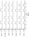
- FIG. 4 is a timing diagram for selected nodes of the high side driver circuit 30 of FIG. 3 .
- the top trace corresponds to the voltage at the node labeled HSD_Gate_1 in FIG. 3 , which is coupled to the gate terminal of a high side MOS switch (not shown in FIG. 3 ).
- the second trace from the top corresponds to the signal HSD_TURNON in FIG. 3 , which is output by the HSD TURN-ON circuit 315.
- the third trace from the top corresponds to the top plate of the capacitor 351, labeled VBOOSTH in FIG. 3 .
- the fourth trace from the top corresponds to node CB_HIGH, the top plate of the bootstrap capacitor 321 in FIG. 3 .
- the fifth trace from the top of FIG. 4 corresponds to the node labeled TURNON_M in FIG. 3 , which controls the high side driver circuit 313.
- the sixth trace from the top of FIG. 4 corresponds to the node CB_LOW in FIG. 3 , which is the bottom plate of the bootstrap capacitor 321.
- the bottom trace in FIG. 4 corresponds to the node VBOOST_L in FIG. 3 , which is the bottom plate of the capacitor 351.
- the timing diagram illustrates the high side driver circuit 30 of FIG. 3 operating over two cycles.
- Time in microseconds
- a capacitor charge phase is shown at time 4.9.
- the bottom plate of the bootstrap capacitor, CB_LOW is approximately zero volts (ground).
- the top plate of the bootstrap capacitor CB_HIGH is at the internal VDD supply voltage or approximately 7 volts during the same time period.
- the bottom plate of the capacitor 351, VBOOSTL is approximately zero volts at time 4.9.
- the top plate of the capacitor 351, VBOOSTH is approximately 7 volts at the same time.
- the two capacitors are charged to the internal supply voltage level during the capacitor charge phase.
- a high side driver turn on phase begins.
- the control signal HSD_TURNON is output by the HSD TURNON circuit 315 in FIG. 3 .
- the Bootstrap Capacitor Charge circuit 319 then couples the input voltage Vin to the bottom plate of the bootstrap capacitor 321, node CB_LOW, which rises to that voltage.
- CB_LOW rises to approximately 17 volts at time 5.02.
- Node CB_HIGH in FIG. 4 illustrates the voltage at the top plate of the bootstrap capacitor 321, and it now rises to the bootstrapped voltage of approximately 22 volts at time 5.02.
- the second shared capacitor 351 also provides a boosted voltage.
- the bottom plate of capacitor 351, node VBOOSTL in FIG. 3 is raised to the same voltage as node CB_HIGH at time 5.02.
- transistor 309 couples the bottom plate of capacitor 351 to the node CB_HIGH in response to a high voltage on control signal HSD _TURNON as shown in FIG. 3 .
- node VBOOSTH rises to the boosted level of approximately 22 volts.
- node TURNON_M rises at time 5.02 in response to the signal VBOOSTH rising.
- This boosted voltage is coupled to the shared gate terminal of the series coupled NMOS transistors within the high side driver circuit 313, and turns them on.
- the output signal HSD_Gate_1 rises to a high voltage at time 5.02 in response to the control signal TURNON_M rising at the gate terminal of the high side driver circuit 313.
- the control signal HSD _TURNON falls.
- the bootstrap capacitor and the capacitor 351 then both enter a charge phase again.
- the control signal TURNON_M also falls at time 5.08.
- the gate signal HSD_Gate_1 remains high until time 5.1.
- the gate capacitance of the high side MOS switch is large enough to keep the gate charged after the high side driver 313 is turned off. In this manner, these examples advantageously allow a charge phase of the bootstrap capacitor 321 to begin, even while the high side MOS switch is still turned on.
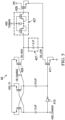
- FIG. 5 shows an example implementation for a Bootstrap Capacitor Charge circuit 40, similar to circuit 319 in FIG. 3 .
- Other circuit implementations could be arranged for use with these examples.
- the circuit 40 has input signals HSD_CHARGE and HSD TURNON.
- HSD_CHARGE when the HSD _CHARGE signal is low, the gate of transistor 411 is at a high voltage due to the operation of inverter 413. The bottom plate of the bootstrap capacitor 421 is thus coupled to ground by transistor 411.
- the node CB_CHARGE at the gate of transistor is at a high level, so the transistor 425 therefore couples the supply voltage VDD_7V to the top plate of the bootstrap capacitor 421, CB_HIGH. In this manner, the bootstrap capacitor is charged.
- the signal CB_CHARGE is also high at this time, as shown in FIG. 3 ; this signal is useful to enable charging of the second bootstrap capacitor such as 351 in FIG. 3 .
- the HSD _TURNON signal is coupled to another back to back series coupled pair of NMOS transistors 427.
- the control input signal HSD_TURNON is at a high voltage
- the voltage at the gate of transistor 429 is coupled by the circuit 427 to the voltage at CB_HIGH and will begin to turn on.
- Voltage VIN is then coupled to the bottom plate of the bootstrap capacitor 421, and the top plate CB_HIGH will be then be "bootstrapped" to the higher voltage, the sum of voltage VIN and supply voltage VDD_7V, as discussed above.
- the transistors 425 and 411 When the control signal HSD _CHARGE in FIG. 5 rises, indicating a high side driver turn on phase is beginning, the transistors 425 and 411 will have a low signal at the gate inputs, and these transistors will turn off and isolate the bootstrap capacitor 421 from the voltage VDD_7V and the ground terminal.
- the signal HSD _TURNON goes high, the bottom plate of the bootstrap capacitor 421 will rise to the voltage VIN, and the top plate of the capacitor 421 will rise to the bootstrapped voltage as described above.
- the circuit 40 efficiently provides a bootstrapped voltage at the node CB_HIGH.
- FIG. 6 is a block diagram of an integrated circuit 611 for forming a two phase step down buck converter 60, in an example that incorporates an integrated shared bootstrap capacitor as described above.
- the two phases are indicated by the two switching nodes SW1 and SW2, which are coupled to the inductors 613 and 615 that drive the output at node Vo.
- the integrated circuit 611 is configured to provide an output voltage of 3.3 volts with 6 amps of current from a range of input voltages that can vary from 4-17 volts as indicated in FIG. 6 .
- FIG. 7 is a block diagram of an integrated circuit 711 for forming a two phase step down buck converter 70, in an example that uses an external component capacitor for the shared bootstrap capacitor described above.
- the two phases are indicated by the two switching node outputs SW1 and SW2 of the integrated circuit 711.
- Inductors 713 and 715 are coupled in parallel to supply current to the output node Vo.
- the output is configured to be 3.3V as in FIG. 6 .
- an input voltage range is 4-17 volts.
- the capacitor 717 is the bootstrap capacitor.
- the integrated circuit 711 is configured to use an external bootstrap capacitor, instead of the integrated bootstrap capacitor of FIG. 6 .
- the terminals CB_HIGH and CB_LOW correspond to these nodes in the circuits shown in FIGS. 2 , 3 and 5 .
- the operation of the circuitry is not otherwise impacted by using an external component as the bootstrap capacitor.
- the buck converter circuit 70 shares the bootstrap capacitor 717 over the two switching stages corresponding to switching nodes SW1, SW2. In other examples, more switching stages are used, and the bootstrap capacitor is shared over multiple stages. Accordingly, in FIG. 7 , the indice "n" is equal to two. However, n may be a positive integer that is greater than or equal to two, including three, four or more stages.
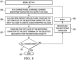
- FIG. 8 is a flow diagram of a method that begins at step 81, where the indice n is set equal to 1.
- step 83 a bootstrap capacitor charge phase is performed, and a bootstrap capacitor is charged to a supply voltage.
- step 85 a high side driver turn on phase begins.
- the charged bootstrap capacitor has a bottom plate coupled to a positive input voltage to create a bootstrapped voltage.
- step 87 the top plate of the charged bootstrap capacitor is coupled to the gate terminal of a selected high side MOS switch for the "nth" switching stage.
- a decision is made about whether all stages have been performed. If additional switching stages remain to be performed, the method continues to step 93, and the bootstrap capacitor is decoupled from the high side switch.
- step 95 the indice n is incremented to advance the method to the next stage.
- the method of FIG. 8 then repeats the bootstrap capacitor charge phase and the high side driver turn on phase for each of the "n" stages. For example, in a two stage case, n begins at 1, the method is performed for the first stage, the indice "n" is incremented to 2, the method is performed for the second stage, and the method then ends
Landscapes
- Engineering & Computer Science (AREA)
- Power Engineering (AREA)
- Dc-Dc Converters (AREA)
- Power Conversion In General (AREA)
Claims (13)
- Abwärtswandler zum Erzeugen einer Ausgangsgleichspannung aus einer Eingangsgleichspannung, umfassend:n Schaltstufen (220, 240), wobei n eine ganze Zahl größer oder gleich zwei ist;einen Ausgangsanschluss (Vo);einen Bootstrap-Kondensator (221, 321); undeine High-Side-Treiber-Einschaltsteuerschaltung (215, 315), wobei jede der n Schaltstufen (220, 240) ferner umfasst:einen High-Side-MOS-Schalter (211, 231), der zwischen einem Eingangsanschluss für eine positive Eingangsspannung (Vin) und einem Schaltknoten (SW1, SW2) geschaltet ist;eine Induktivität (223, 243), die zwischen dem Schaltknoten (SW1, SW2) und dem Ausgangsanschluss (Vo) geschaltet ist; undeinen High-Side-Treiber (213, 313; 233, 333), umfassend:einen Gate- Verbindungsanschluss; undein Paar Rücken-an-Rücken angeordnete NMOS-Transistoren, die zwischen einer oberen Platte des Bootstrap-Kondensators (221, 321) undeinem Gate-Anschluss des High-Side-MOS-Schalters (211, 231) geschaltet sind, wobei ein Gate-Anschluss jedes der Rücken-an-Rücken angeordneten NMOS-Transistoren mit dem Gate-Verbindungsanschluss verbunden ist,wobei die High-Side-Treiber-Einschaltsteuerschaltung (215, 315) mit dem Gate-Verbindungsanschluss des High-Side-Treibers (213, 313; 233, 333) jeder der n Schaltstufen (220, 240) verbunden ist, und dazu ausgelegt ist, den High-Side-Treiber (213, 313; 233, 333) einer der n Schaltstufen (220, 240) auszuwählen; undwobei der ausgewählte High-Side-Treiber (213, 313; 233, 333) dazu ausgelegt ist, bei einer Auswahl den Bootstrap-Kondensator (221, 321) mit einem Gate-Anschluss des jeweiligen High-Side-MOS-Schalters (211, 231) zu verbinden, wobei der Bootstrap-Kondensator (221, 321) dazu ausgelegt ist, eine Gate-Kapazität des jeweiligen High-Side-MOS-Schalters (211, 231) zu laden.
- Abwärtswandler nach Anspruch 1, wobei der High-Side-MOS-Schalter (211, 231) in jeder der n Schaltstufen (220, 240) ein NMOS-Transistor ist.
- Abwärtswandler nach Anspruch 1, ferner umfassend eine Ladeschaltung (219, 319) für den Bootstrap-Kondensator (221), die dazu ausgelegt ist, eine obere Platte des Bootstrap-Kondensators (221, 321) selektiv mit einer positiven Versorgungsspannung zu verbinden und selektiv eine untere Platte des Bootstrap-Kondensators (221, 321) mit einem Erdpotential zu verbinden.
- Integrierter Schaltkreis, umfassend eine Abwärtskonfiguration nach Anspruch 1, wobei die High-Side-MOS-Schaltvorrichtung eine NMOS-Schaltvorrichtung mit einem Gate-Anschluss ist und zwischen dem positiven Eingangsspannungsanschluss und dem entsprechenden Schaltknotenausgang geschaltet ist; und umfassend:eine Low-Side-NMOS-Schaltvorrichtung mit einem Gate-Anschluss, der zwischen dem entsprechenden Schaltknotenausgang und einem Erdungsanschluss geschaltet ist;wobei der High-Side-Treiber, der selektiv eine obere Platte eines Bootstrap-Kondensators (221, 321) mit dem Gate-Anschluss der High-Side-NMOS-Schaltvorrichtung verbindet, auf einen Steuereingang reagiert, und wobei die High-Side-Treibersteuerschaltung mit dem Steuereingang des High-Side-Treibers jeder der n Schaltstufen (220, 240) verbunden ist;wobei der Bootstrap-Kondensator (221, 321) von den n Schaltstufen (220, 240) gemeinsam verwendet wird.
- Integrierter Schaltkreis nach Anspruch 4, und ferner umfassend: Bootstrap-Ladeschaltkreise (219, 319), die selektiv mit dem Bootstrap-Kondensator (221, 321) verbunden sind und dazu ausgelegt sind, selektiv die obere Platte des Bootstrap-Kondensators (221, 321) mit einer positiven Versorgungsspannung zu verbinden und selektiv eine untere Platte des Bootstrap-Kondensators (221, 321) mit einem Erdpotential zu verbinden.
- Integrierter Schaltkreis nach Anspruch 4, wobei die High-Side-Treibersteuerschaltung dazu ausgelegt ist, die obere Platte des Bootstrap-Kondensators (221, 321) selektiv mit der High-Side-NMOS-Schaltvorrichtung einer ausgewählten der n Schaltstufen (220, 240) zu verbinden und selektiv eine untere Platte des Bootstrap-Kondensators (221, 321) mit dem positiven Eingangsspannungsanschluss zu verbinden.
- Integrierter Schaltkreis nach Anspruch 4, wobei jeder der High-Side-Treiber (211, 231) in den n Schaltstufen (220, 240) ferner ein Paar NMOS-Transistoren aufweist, die Rücken-an-Rücken in Reihe geschaltet sind, und das Paar NMOS-Transistoren einen gemeinsamen Gate-Anschluss hat, der mit dem Steuereingang verbunden ist.
- Integrierter Schaltkreis nach Anspruch 4, und ferner umfassend n Induktivitäten (223, 243), die jeweils mit einem entsprechenden der n Schaltausgänge verbunden sind, wobei die n Induktivitäten (223, 243) parallel zwischen den n Schaltknoten und einem Spannungsausgangsknoten geschaltet sind, um einen Gleichspannungsausgangsanschluss (Vo) für einen Abwärtswandler zu bilden.
- Verfahren, umfassend:Laden eines Bootstrap-Kondensators (221, 321) eines Abwärtswandlers nach Anspruch 1 durch Verbinden einer oberen Platte des Bootstrap-Kondensators (221, 321) mit einer positiven Spannungsversorgung, während eine untere Platte des Bootstrap-Kondensators (221, 321) mit einem Erdpotential verbunden wird; undanschließendes Verbinden der unteren Platte des Bootstrap-Kondensators (221, 321) mit der Eingangsspannung, während gleichzeitig die obere Platte des Bootstrap-Kondensators (221, 321) mit einem Gate-Anschluss eines High-Side-NMOS-Schalters innerhalb einer ausgewählten von n Schaltstufen (220, 240) verbunden wird, um innerhalb der ausgewählten der n Schaltstufen (220, 240) eine Bootstrap-Spannung bereitzustellen, die größer als die Eingangsspannung am Gate-Anschluss des High-Side-NMOS-Schalters ist, um so den High-Side-NMOS-Schalter einzuschalten.
- Verfahren nach Anspruch 9, ferner umfassend:Trennen des Bootstrap-Kondensators (221, 321) von der ausgewählten der n Schaltstufen (220, 240);anschließendes Wiederaufladen des Bootstrap-Kondensators (221, 321) durch erneutes Verbinden einer oberen Platte des Bootstrap-Kondensators (221, 321) mit der positiven Spannungsversorgung, während eine untere Platte des Bootstrap-Kondensators (221, 321) mit einem Erdpotential verbunden wird;anschließendes Verbinden der unteren Platte des Bootstrap-Kondensators (221, 321) mit der Eingangsspannung, während gleichzeitig die obere Platte des Bootstrap-Kondensators (221, 321) mit einem Gate-Anschluss eines anderen der High-Side-NMOS-Schalter innerhalb eines anderen ausgewählten Schalters der n Schaltstufen (220, 240) verbunden wird, um eine Spannung bereitzustellen, die größer als die Eingangsspannung am Gate-Anschluss ist, um so den High-Side-NMOS-Schalter innerhalb der anderen ausgewählten der n Schaltstufen (220, 240) einzuschalten; undanschließendes Wiederholen der drei oben aufgeführten Schritte, bis jede der n Schaltstufen (220, 240) mit dem Bootstrap-Kondensator (221, 321) verbunden wurde, während dieser geladen wird.
- Verfahren nach Anspruch 9, wobei das anschließende Verbinden der unteren Platte des Bootstrap-Kondensators (221, 321) mit der Eingangsspannung, während gleichzeitig die obere Platte des Bootstrap-Kondensators (221, 321) mit einem Gate-Anschluss eines ausgewählten der High-Side-NMOS-Schalter verbunden wird, ferner aufweist:
Verbinden eines Paares von Rücken-an-Rücken in Reihe geschalteten NMOS-Transistoren zwischen der oberen Platte des Bootstrap-Kondensators (221, 321) und dem Gate-Anschluss des High-Side-NMOS-Schalters für die ausgewählte der n Schaltstufen (220, 240), und Betreiben des Paares von Rücken-an-Rücken in Reihe geschalteten NMOS-Transistoren durch Anlegen einer Spannung größer als eine vorbestimmte Gate-Schwellenspannung an einen gemeinsamen Gate-Anschluss des Paares von Rücken-an-Rücken in Reihe geschalteten NMOS-Transistoren, um das Paar Rücken-an-Rücken in Reihe geschalteter NMOS-Transistoren einzuschalten. - Integrierter Schaltkreis nach Anspruch 6, wobei die n Schaltstufen (220, 240) und der Bootstrap-Kondensator (221, 321) auf einem einzigen integrierten Schaltkreis vorgesehen sind.
- Integrierter Schaltkreis nach Anspruch 6, wobei die n Schaltstufen (220, 240) auf einem einzigen integrierten Schaltkreis vorgesehen sind und der Bootstrap-Kondensator (221, 321) als externe Komponente vorgesehen ist, die mit dem integrierten Schaltkreis verbunden ist.
Applications Claiming Priority (2)
| Application Number | Priority Date | Filing Date | Title |
|---|---|---|---|
| US14/456,745 US9419509B2 (en) | 2014-08-11 | 2014-08-11 | Shared bootstrap capacitor for multiple phase buck converter circuit and methods |
| PCT/US2015/044707 WO2016025514A1 (en) | 2014-08-11 | 2015-08-11 | Shared bootstrap capacitor for multiple phase buck converter circuit and methods |
Publications (3)
| Publication Number | Publication Date |
|---|---|
| EP3205008A1 EP3205008A1 (de) | 2017-08-16 |
| EP3205008A4 EP3205008A4 (de) | 2018-08-15 |
| EP3205008B1 true EP3205008B1 (de) | 2024-09-11 |
Family
ID=55268178
Family Applications (1)
| Application Number | Title | Priority Date | Filing Date |
|---|---|---|---|
| EP15831490.6A Active EP3205008B1 (de) | 2014-08-11 | 2015-08-11 | Gemeinsam verwendeter bootstrap-kondensator für mehrphasige abwärtswandlerschaltung und verfahren |
Country Status (5)
| Country | Link |
|---|---|
| US (1) | US9419509B2 (de) |
| EP (1) | EP3205008B1 (de) |
| JP (1) | JP6685282B2 (de) |
| CN (1) | CN106664020B (de) |
| WO (1) | WO2016025514A1 (de) |
Families Citing this family (40)
| Publication number | Priority date | Publication date | Assignee | Title |
|---|---|---|---|---|
| WO2014119307A1 (ja) * | 2013-01-31 | 2014-08-07 | パナソニック株式会社 | Dc/dcコンバータ |
| JP2016086616A (ja) * | 2014-10-29 | 2016-05-19 | 株式会社アイケイエス | 電力変換器 |
| US9871444B2 (en) * | 2014-12-24 | 2018-01-16 | Texas Instruments Incorporated | Integrated circuit with configurable control and power switches |
| US10256812B2 (en) * | 2016-07-08 | 2019-04-09 | Infineon Technologies Austria Ag | Half bridge coupled resonant gate drivers |
| US9917510B2 (en) * | 2016-07-21 | 2018-03-13 | Dialog Semiconductor (Uk) Limited | Multi-staged buck converter with efficient low power operation |
| CN107800294B (zh) * | 2016-08-31 | 2019-08-13 | 台达电子企业管理(上海)有限公司 | 交错并联电路、功率集成模块及功率集成芯片 |
| US10620654B2 (en) * | 2016-08-31 | 2020-04-14 | Delta Electronics (Shanghai) Co., Ltd | Alternatingly-switched parallel circuit, integrated power module and integrated power package |
| JP2018046685A (ja) * | 2016-09-15 | 2018-03-22 | ルネサスエレクトロニクス株式会社 | 半導体装置および電力制御装置 |
| US10693449B2 (en) | 2016-09-23 | 2020-06-23 | Tohoku University | Switching circuit device, step-down DC-DC converter, and element unit |
| US10079538B2 (en) * | 2016-10-18 | 2018-09-18 | Texas Instruments Incorporated | Bootstrap circuit for DC/DC converter |
| US10389257B2 (en) * | 2016-10-21 | 2019-08-20 | Skyworks Solutions, Inc. | Switch efficiency optimization circuit |
| US10014775B1 (en) * | 2016-12-27 | 2018-07-03 | Texas Instruments Incorporated | Methods and apparatus for full gate drive of multilevel DC-DC converter with full duty cycle operation |
| USRE50103E1 (en) | 2017-04-14 | 2024-08-27 | Lion Semiconductor Inc. | Circuits for a hybrid switched capacitor converter |
| CN113890332B (zh) * | 2017-09-05 | 2024-12-10 | 莱恩半导体股份有限公司 | 用于混合开关式电容器转换器的电路 |
| US10381918B1 (en) * | 2018-02-19 | 2019-08-13 | Microchip Technology Incorporated | Multi-phase parallelable constant on time buck controller with phase interleaving ensured by ripple injection |
| US10263516B1 (en) * | 2018-03-06 | 2019-04-16 | Infineon Technologies Austria Ag | Cascaded voltage converter with inter-stage magnetic power coupling |
| US10256729B1 (en) * | 2018-03-06 | 2019-04-09 | Infineon Technologies Austria Ag | Switched-capacitor converter with interleaved half bridge |
| CN114362538A (zh) | 2018-04-27 | 2022-04-15 | 华为技术有限公司 | 一种电源电路及装置 |
| US20210328514A1 (en) * | 2018-09-07 | 2021-10-21 | Magna International Inc. | Dual dc-dc converter |
| JP7265344B2 (ja) * | 2018-11-09 | 2023-04-26 | ローム株式会社 | 電源ic及び電源回路 |
| WO2020119817A1 (en) * | 2018-12-14 | 2020-06-18 | Huawei Technologies Co., Ltd. | Shared bootstrap capacitor system and method |
| US11949328B2 (en) * | 2019-01-28 | 2024-04-02 | Murata Manufacturing Co., Ltd. | Bootstrap pre-charge circuit in totem-pole power factor correction converter |
| US10784764B2 (en) * | 2019-02-01 | 2020-09-22 | Texas Instruments Incorporated | Switched-mode DC/DC converter having a bootstrapped high-side driver |
| US10637355B1 (en) | 2019-05-10 | 2020-04-28 | Nxp B.V. | Switched capacitor voltage converter and method for operating a switched capacitor voltage converter |
| US10811959B1 (en) | 2019-05-10 | 2020-10-20 | Nxp B.V. | Switched capacitor voltage converter and method for operating a switched capacitor voltage converter |
| CN113841326B (zh) * | 2019-06-24 | 2024-02-13 | 德州仪器公司 | 具有多个驱动级的开关转换器及相关模式 |
| US10886851B1 (en) | 2019-09-13 | 2021-01-05 | Apple Inc. | Voltage regulator with multi-level, multi-phase buck architecture |
| US11532428B2 (en) | 2019-09-18 | 2022-12-20 | Delta Electronics, Inc. | Power conversion system and magnetic component thereof |
| CN112532049B (zh) * | 2019-09-18 | 2022-04-05 | 台达电子工业股份有限公司 | 电源转换系统 |
| US11309878B2 (en) | 2019-09-18 | 2022-04-19 | Delta Electronics, Inc. | Power conversion system |
| US11205963B2 (en) | 2019-09-18 | 2021-12-21 | Delta Electronics, Inc. | Multiphase buck converter with extended duty cycle range using multiple bootstrap capacitors |
| US11205958B2 (en) | 2019-09-18 | 2021-12-21 | Delta Electronics, Inc. | Power conversion system |
| CN112532027B (zh) * | 2019-09-18 | 2021-12-03 | 圣邦微电子(北京)股份有限公司 | 一种多级功率管驱动电路 |
| US11658572B2 (en) | 2020-06-11 | 2023-05-23 | Intel Corporation | Power field effect transistor topology and bootstrap circuit for inverting buck-boost DC-DC converter |
| CN113972815B (zh) * | 2020-07-24 | 2024-07-05 | 茂睿芯(深圳)科技有限公司 | 双通道栅极驱动电路和双通道栅极驱动芯片 |
| KR102947362B1 (ko) | 2020-11-23 | 2026-04-03 | 삼성전자주식회사 | 멀티플렉서 및 이를 포함하는 반도체 장치 |
| US11641163B2 (en) * | 2021-08-11 | 2023-05-02 | Monolithic Power Systems, Inc. | Trans-inductor voltage regulator with averaging inductor DCR current sensing |
| US12323045B2 (en) * | 2022-12-15 | 2025-06-03 | Renesas Design (UK) Limited | Driver stage with an intermediate circuit |
| CN116995929B (zh) * | 2023-09-25 | 2025-02-18 | 联宝(合肥)电子科技有限公司 | 一种主板供电模块、供电方法、电源设备和电子设备 |
| US20250309752A1 (en) * | 2024-03-28 | 2025-10-02 | Nexperia B.V. | BOOT UVLO detection scheme for high voltage applications |
Citations (1)
| Publication number | Priority date | Publication date | Assignee | Title |
|---|---|---|---|---|
| US7904864B2 (en) * | 2006-10-07 | 2011-03-08 | Active-Semi, Inc. | Interconnect layer of a modularly designed analog integrated circuit |
Family Cites Families (50)
| Publication number | Priority date | Publication date | Assignee | Title |
|---|---|---|---|---|
| US5627460A (en) * | 1994-12-28 | 1997-05-06 | Unitrode Corporation | DC/DC converter having a bootstrapped high side driver |
| US6201717B1 (en) * | 1999-09-04 | 2001-03-13 | Texas Instruments Incorporated | Charge-pump closely coupled to switching converter |
| US6362608B1 (en) * | 2001-02-01 | 2002-03-26 | Maxim Integrated Products, Inc. | Multi-phase switching converters and methods |
| US6903535B2 (en) * | 2002-04-16 | 2005-06-07 | Arques Technology, Inc. | Biasing system and method for low voltage DC—DC converters with built-in N-FETs |
| JP3556648B2 (ja) * | 2002-07-08 | 2004-08-18 | 日本テキサス・インスツルメンツ株式会社 | Dc−dcコンバータ及びdc−dcコンバータの制御回路 |
| US6670794B1 (en) | 2002-07-12 | 2003-12-30 | Richtek Technology Corp. | Multi-phase DC-to-DC buck converter with multi-phase current balance and adjustable load regulation |
| FR2858493B1 (fr) * | 2003-07-31 | 2005-10-21 | St Microelectronics Sa | Circuit d'attaque a autoelevation |
| US7061215B2 (en) * | 2003-10-02 | 2006-06-13 | Intersil Americas Inc. | Cascadable current-mode regulator |
| US7215189B2 (en) * | 2003-11-12 | 2007-05-08 | International Rectifier Corporation | Bootstrap diode emulator with dynamic back-gate biasing |
| JP4477952B2 (ja) * | 2004-07-09 | 2010-06-09 | 株式会社ルネサステクノロジ | 半導体装置、dc/dcコンバータおよび電源システム |
| US20060044051A1 (en) * | 2004-08-24 | 2006-03-02 | International Rectifier Corporation | Bootstrap diode emulator with dynamic back-gate biasing and short-circuit protection |
| US7215102B2 (en) * | 2005-04-20 | 2007-05-08 | Intersil Americas Inc. | Semi-clockless, cascaded, current-mode power regulator having high noise immunity and arbitrary phase count |
| ITMI20052055A1 (it) * | 2005-10-27 | 2007-04-28 | St Microelectronics Srl | Dispositivo di controllo per un convertitore a commutazione e relativo convertitore a commutazione |
| JP4229177B2 (ja) | 2006-11-30 | 2009-02-25 | ミツミ電機株式会社 | マルチフェーズdc−dcコンバータ |
| TW200835125A (en) * | 2007-02-08 | 2008-08-16 | Richtek Techohnology Corp | Circuit for charging the boot-strap capacitor of voltage converter |
| US7592831B2 (en) * | 2007-04-05 | 2009-09-22 | International Rectifier Corporation | Circuit to optimize charging of bootstrap capacitor with bootstrap diode emulator |
| US7518352B2 (en) * | 2007-05-11 | 2009-04-14 | Freescale Semiconductor, Inc. | Bootstrap clamping circuit for DC/DC regulators and method thereof |
| US20080290841A1 (en) * | 2007-05-23 | 2008-11-27 | Richtek Technology Corporation | Charging Circuit for Bootstrap Capacitor and Integrated Driver Circuit Using Same |
| JP4916964B2 (ja) * | 2007-07-12 | 2012-04-18 | ルネサスエレクトロニクス株式会社 | Dc−dcコンバータ、ドライバic、およびシステムインパッケージ |
| US7882482B2 (en) * | 2007-10-12 | 2011-02-01 | Monolithic Power Systems, Inc. | Layout schemes and apparatus for high performance DC-DC output stage |
| US7808222B2 (en) | 2007-10-12 | 2010-10-05 | Monolithic Power Systems, Inc. | Method and apparatus for high performance switch mode voltage regulators |
| US8030908B2 (en) * | 2007-12-13 | 2011-10-04 | Upi Semiconductor Corporation | Control method for multi-phase DC-DC controller and multi-phase DC-DC controller |
| JP5297104B2 (ja) * | 2008-07-01 | 2013-09-25 | ルネサスエレクトロニクス株式会社 | 半導体装置 |
| US8207720B2 (en) * | 2008-07-18 | 2012-06-26 | Infineon Technologies Austria Ag | Methods and apparatus for power supply load dump compensation |
| JP5458686B2 (ja) | 2009-06-16 | 2014-04-02 | 日本テキサス・インスツルメンツ株式会社 | 降圧型コンバータ |
| JP5330962B2 (ja) * | 2009-11-04 | 2013-10-30 | パナソニック株式会社 | Dc−dcコンバータ |
| US8680895B2 (en) * | 2010-10-08 | 2014-03-25 | Texas Instruments Incorporated | Controlling power chain with same controller in either of two different applications |
| EP2721733B1 (de) * | 2011-06-14 | 2019-02-20 | Infineon Technologies Austria AG | Gate-treiber für leistungstransistor |
| JP5794855B2 (ja) * | 2011-08-05 | 2015-10-14 | トランスフォーム・ジャパン株式会社 | 電源装置の駆動回路及び電源装置 |
| JP2013070263A (ja) * | 2011-09-22 | 2013-04-18 | Renesas Electronics Corp | 電力変換回路、多相ボルテージレギュレータ、及び電力変換方法 |
| US8970185B1 (en) * | 2011-10-03 | 2015-03-03 | Marvell International Ltd. | Method for maintaining high efficiency power conversion in DC-DC switching regulators over wide input supply range |
| US20130106374A1 (en) * | 2011-11-02 | 2013-05-02 | Alan R. Ball | Power supply controller and method therefor |
| JP6071205B2 (ja) * | 2012-02-02 | 2017-02-01 | 株式会社ソニー・インタラクティブエンタテインメント | Dc/dcコンバータ |
| JP2013162585A (ja) * | 2012-02-02 | 2013-08-19 | Sony Computer Entertainment Inc | Dc/dcコンバータ |
| TWI463798B (zh) * | 2012-04-05 | 2014-12-01 | Anpec Electronics Corp | 責任週期產生器及電源轉換器 |
| TW201347381A (zh) * | 2012-05-03 | 2013-11-16 | Anpec Electronics Corp | 應用於靴帶電路之直流轉換器 |
| US8842225B2 (en) * | 2012-05-14 | 2014-09-23 | Rohm Co., Ltd. | Switching power supply device |
| TW201404023A (zh) * | 2012-07-12 | 2014-01-16 | Anpec Electronics Corp | 靴帶電路 |
| US8917076B2 (en) * | 2012-08-10 | 2014-12-23 | Monolithic Power Systems, Inc. | Off-line regulator with pass device and associated method |
| CN102832810B (zh) * | 2012-08-30 | 2015-04-08 | 成都芯源系统有限公司 | 自举电压刷新控制电路、电压转换电路及相关控制方法 |
| JP6075532B2 (ja) * | 2012-09-03 | 2017-02-08 | セイコーエプソン株式会社 | 容量性負荷駆動回路、液体噴射型印刷装置、液体噴射装置、流体輸送装置および医療機器 |
| US9479055B2 (en) * | 2012-12-03 | 2016-10-25 | Panasonic Intellectual Property Management Co., Ltd. | DC-DC converter |
| US8502511B1 (en) * | 2013-01-03 | 2013-08-06 | Richtek Technology Corporation | Buck switching regulator |
| WO2014119307A1 (ja) | 2013-01-31 | 2014-08-07 | パナソニック株式会社 | Dc/dcコンバータ |
| US9484758B2 (en) | 2013-02-05 | 2016-11-01 | Apple Inc. | Hybrid bootstrap capacitor refresh technique for charger/converter |
| JP6162510B2 (ja) * | 2013-07-03 | 2017-07-12 | 株式会社ソニー・インタラクティブエンタテインメント | 降圧dc/dcコンバータ、そのコントローラおよび制御方法、ならびにそれを用いた電子機器 |
| TWM472362U (zh) * | 2013-08-07 | 2014-02-11 | Richtek Technology Corp | 降壓型切換式電源供應器 |
| EP2849323B1 (de) * | 2013-09-17 | 2016-04-20 | Dialog Semiconductor GmbH | Steuerungsschaltung für mehrere spannungsseitige Schalter |
| US9548648B2 (en) * | 2014-04-25 | 2017-01-17 | Texas Instruments Incorporated | Switched reference MOSFET drive assist circuit |
| US9306458B2 (en) * | 2014-04-25 | 2016-04-05 | Texas Instruments Incorporated | Adaptive boost driver charging circuit |
-
2014
- 2014-08-11 US US14/456,745 patent/US9419509B2/en active Active
-
2015
- 2015-08-11 JP JP2017507964A patent/JP6685282B2/ja active Active
- 2015-08-11 EP EP15831490.6A patent/EP3205008B1/de active Active
- 2015-08-11 WO PCT/US2015/044707 patent/WO2016025514A1/en not_active Ceased
- 2015-08-11 CN CN201580040047.3A patent/CN106664020B/zh active Active
Patent Citations (1)
| Publication number | Priority date | Publication date | Assignee | Title |
|---|---|---|---|---|
| US7904864B2 (en) * | 2006-10-07 | 2011-03-08 | Active-Semi, Inc. | Interconnect layer of a modularly designed analog integrated circuit |
Also Published As
| Publication number | Publication date |
|---|---|
| EP3205008A4 (de) | 2018-08-15 |
| CN106664020A (zh) | 2017-05-10 |
| EP3205008A1 (de) | 2017-08-16 |
| JP6685282B2 (ja) | 2020-04-22 |
| JP2017530669A (ja) | 2017-10-12 |
| US9419509B2 (en) | 2016-08-16 |
| CN106664020B (zh) | 2020-01-21 |
| WO2016025514A1 (en) | 2016-02-18 |
| US20160043624A1 (en) | 2016-02-11 |
Similar Documents
| Publication | Publication Date | Title |
|---|---|---|
| EP3205008B1 (de) | Gemeinsam verwendeter bootstrap-kondensator für mehrphasige abwärtswandlerschaltung und verfahren | |
| US11101735B2 (en) | Three-level converter using an auxiliary switched capacitor circuit | |
| US9013165B2 (en) | Switching regulator including a configurable multi-mode PWM controller implementing multiple control schemes | |
| EP3485561B1 (de) | Ansteuerung von ladungspumpenschaltkreisen | |
| US20200373841A1 (en) | Wide switching frequency range switched mode power supply control topology | |
| US8803500B2 (en) | PFM SMPS with quick sudden load change response | |
| US7737767B2 (en) | Control circuit and control method for charge pump circuit | |
| TWI404317B (zh) | 雙極性雙輸出同步升壓變換器及其操作方法 | |
| EP2973971B1 (de) | Systeme und verfahren für 100-prozent-arbeitszyklus bei schaltreglern | |
| US9083251B2 (en) | Power controller with pulse skipping | |
| KR101820232B1 (ko) | 전력 변환기 회로를 동작시키기 위한 방법 및 전력 변환기 회로 | |
| CN1938926A (zh) | 提供具有与电容器成比例的电流的电流调节电荷泵驱动器的集成设备 | |
| CN102761255A (zh) | 开关电源装置 | |
| CN112889210B (zh) | 双电源低侧门驱动器 | |
| US10110129B2 (en) | Switching control circuit, switching power supply device and electronic apparatus | |
| EP3180845B1 (de) | Geschaltete leistungsstufe und verfahren zur steuerung davon | |
| EP1879284B1 (de) | DC-DC-Wandler und Netzteilvorrichtung | |
| US7804698B2 (en) | Switched capacitor controller and method therefor | |
| US9209691B2 (en) | Fast transient buck regulator with dynamic charge/discharge capability | |
| US10775816B2 (en) | Method of forming a semiconductor device | |
| WO2008027038A1 (en) | Charge pump controller and method therefor | |
| US20180092171A1 (en) | Led drive circuit | |
| WO2018051086A1 (en) | Dc-dc converters |
Legal Events
| Date | Code | Title | Description |
|---|---|---|---|
| STAA | Information on the status of an ep patent application or granted ep patent |
Free format text: STATUS: THE INTERNATIONAL PUBLICATION HAS BEEN MADE |
|
| PUAI | Public reference made under article 153(3) epc to a published international application that has entered the european phase |
Free format text: ORIGINAL CODE: 0009012 |
|
| STAA | Information on the status of an ep patent application or granted ep patent |
Free format text: STATUS: REQUEST FOR EXAMINATION WAS MADE |
|
| 17P | Request for examination filed |
Effective date: 20170630 |
|
| AK | Designated contracting states |
Kind code of ref document: A1 Designated state(s): AL AT BE BG CH CY CZ DE DK EE ES FI FR GB GR HR HU IE IS IT LI LT LU LV MC MK MT NL NO PL PT RO RS SE SI SK SM TR |
|
| AX | Request for extension of the european patent |
Extension state: BA ME |
|
| DAV | Request for validation of the european patent (deleted) | ||
| DAX | Request for extension of the european patent (deleted) | ||
| A4 | Supplementary search report drawn up and despatched |
Effective date: 20180713 |
|
| RIC1 | Information provided on ipc code assigned before grant |
Ipc: H02M 3/158 20060101AFI20180709BHEP Ipc: H03K 17/06 20060101ALI20180709BHEP Ipc: H02M 1/084 20060101ALI20180709BHEP Ipc: H03K 17/61 20060101ALI20180709BHEP Ipc: H02M 3/00 20060101ALN20180709BHEP |
|
| STAA | Information on the status of an ep patent application or granted ep patent |
Free format text: STATUS: EXAMINATION IS IN PROGRESS |
|
| 17Q | First examination report despatched |
Effective date: 20190916 |
|
| RIC1 | Information provided on ipc code assigned before grant |
Ipc: H02M 3/00 20060101ALN20230920BHEP Ipc: H03K 17/61 20060101ALI20230920BHEP Ipc: H03K 17/06 20060101ALI20230920BHEP Ipc: H02M 1/084 20060101ALI20230920BHEP Ipc: H02M 3/158 20060101AFI20230920BHEP |
|
| GRAP | Despatch of communication of intention to grant a patent |
Free format text: ORIGINAL CODE: EPIDOSNIGR1 |
|
| STAA | Information on the status of an ep patent application or granted ep patent |
Free format text: STATUS: GRANT OF PATENT IS INTENDED |
|
| RIC1 | Information provided on ipc code assigned before grant |
Ipc: H02M 3/00 20060101ALN20240312BHEP Ipc: H03K 17/61 20060101ALI20240312BHEP Ipc: H03K 17/06 20060101ALI20240312BHEP Ipc: H02M 1/084 20060101ALI20240312BHEP Ipc: H02M 3/158 20060101AFI20240312BHEP |
|
| INTG | Intention to grant announced |
Effective date: 20240326 |
|
| P01 | Opt-out of the competence of the unified patent court (upc) registered |
Effective date: 20240415 |
|
| GRAS | Grant fee paid |
Free format text: ORIGINAL CODE: EPIDOSNIGR3 |
|
| GRAA | (expected) grant |
Free format text: ORIGINAL CODE: 0009210 |
|
| STAA | Information on the status of an ep patent application or granted ep patent |
Free format text: STATUS: THE PATENT HAS BEEN GRANTED |
|
| AK | Designated contracting states |
Kind code of ref document: B1 Designated state(s): AL AT BE BG CH CY CZ DE DK EE ES FI FR GB GR HR HU IE IS IT LI LT LU LV MC MK MT NL NO PL PT RO RS SE SI SK SM TR |
|
| REG | Reference to a national code |
Ref country code: GB Ref legal event code: FG4D |
|
| REG | Reference to a national code |
Ref country code: CH Ref legal event code: EP |
|
| REG | Reference to a national code |
Ref country code: DE Ref legal event code: R096 Ref document number: 602015089876 Country of ref document: DE |
|
| REG | Reference to a national code |
Ref country code: IE Ref legal event code: FG4D |
|
| REG | Reference to a national code |
Ref country code: LT Ref legal event code: MG9D |
|
| PG25 | Lapsed in a contracting state [announced via postgrant information from national office to epo] |
Ref country code: NO Free format text: LAPSE BECAUSE OF FAILURE TO SUBMIT A TRANSLATION OF THE DESCRIPTION OR TO PAY THE FEE WITHIN THE PRESCRIBED TIME-LIMIT Effective date: 20241211 |
|
| REG | Reference to a national code |
Ref country code: NL Ref legal event code: MP Effective date: 20240911 |
|
| PG25 | Lapsed in a contracting state [announced via postgrant information from national office to epo] |
Ref country code: GR Free format text: LAPSE BECAUSE OF FAILURE TO SUBMIT A TRANSLATION OF THE DESCRIPTION OR TO PAY THE FEE WITHIN THE PRESCRIBED TIME-LIMIT Effective date: 20241212 Ref country code: FI Free format text: LAPSE BECAUSE OF FAILURE TO SUBMIT A TRANSLATION OF THE DESCRIPTION OR TO PAY THE FEE WITHIN THE PRESCRIBED TIME-LIMIT Effective date: 20240911 |
|
| PG25 | Lapsed in a contracting state [announced via postgrant information from national office to epo] |
Ref country code: BG Free format text: LAPSE BECAUSE OF FAILURE TO SUBMIT A TRANSLATION OF THE DESCRIPTION OR TO PAY THE FEE WITHIN THE PRESCRIBED TIME-LIMIT Effective date: 20240911 |
|
| PG25 | Lapsed in a contracting state [announced via postgrant information from national office to epo] |
Ref country code: LV Free format text: LAPSE BECAUSE OF FAILURE TO SUBMIT A TRANSLATION OF THE DESCRIPTION OR TO PAY THE FEE WITHIN THE PRESCRIBED TIME-LIMIT Effective date: 20240911 |
|
| PG25 | Lapsed in a contracting state [announced via postgrant information from national office to epo] |
Ref country code: HR Free format text: LAPSE BECAUSE OF FAILURE TO SUBMIT A TRANSLATION OF THE DESCRIPTION OR TO PAY THE FEE WITHIN THE PRESCRIBED TIME-LIMIT Effective date: 20240911 |
|
| PG25 | Lapsed in a contracting state [announced via postgrant information from national office to epo] |
Ref country code: RS Free format text: LAPSE BECAUSE OF FAILURE TO SUBMIT A TRANSLATION OF THE DESCRIPTION OR TO PAY THE FEE WITHIN THE PRESCRIBED TIME-LIMIT Effective date: 20241211 Ref country code: ES Free format text: LAPSE BECAUSE OF FAILURE TO SUBMIT A TRANSLATION OF THE DESCRIPTION OR TO PAY THE FEE WITHIN THE PRESCRIBED TIME-LIMIT Effective date: 20240911 |
|
| PG25 | Lapsed in a contracting state [announced via postgrant information from national office to epo] |
Ref country code: RS Free format text: LAPSE BECAUSE OF FAILURE TO SUBMIT A TRANSLATION OF THE DESCRIPTION OR TO PAY THE FEE WITHIN THE PRESCRIBED TIME-LIMIT Effective date: 20241211 Ref country code: NO Free format text: LAPSE BECAUSE OF FAILURE TO SUBMIT A TRANSLATION OF THE DESCRIPTION OR TO PAY THE FEE WITHIN THE PRESCRIBED TIME-LIMIT Effective date: 20241211 Ref country code: LV Free format text: LAPSE BECAUSE OF FAILURE TO SUBMIT A TRANSLATION OF THE DESCRIPTION OR TO PAY THE FEE WITHIN THE PRESCRIBED TIME-LIMIT Effective date: 20240911 Ref country code: HR Free format text: LAPSE BECAUSE OF FAILURE TO SUBMIT A TRANSLATION OF THE DESCRIPTION OR TO PAY THE FEE WITHIN THE PRESCRIBED TIME-LIMIT Effective date: 20240911 Ref country code: GR Free format text: LAPSE BECAUSE OF FAILURE TO SUBMIT A TRANSLATION OF THE DESCRIPTION OR TO PAY THE FEE WITHIN THE PRESCRIBED TIME-LIMIT Effective date: 20241212 Ref country code: FI Free format text: LAPSE BECAUSE OF FAILURE TO SUBMIT A TRANSLATION OF THE DESCRIPTION OR TO PAY THE FEE WITHIN THE PRESCRIBED TIME-LIMIT Effective date: 20240911 Ref country code: ES Free format text: LAPSE BECAUSE OF FAILURE TO SUBMIT A TRANSLATION OF THE DESCRIPTION OR TO PAY THE FEE WITHIN THE PRESCRIBED TIME-LIMIT Effective date: 20240911 Ref country code: BG Free format text: LAPSE BECAUSE OF FAILURE TO SUBMIT A TRANSLATION OF THE DESCRIPTION OR TO PAY THE FEE WITHIN THE PRESCRIBED TIME-LIMIT Effective date: 20240911 |
|
| REG | Reference to a national code |
Ref country code: AT Ref legal event code: MK05 Ref document number: 1723574 Country of ref document: AT Kind code of ref document: T Effective date: 20240911 |
|
| PG25 | Lapsed in a contracting state [announced via postgrant information from national office to epo] |
Ref country code: NL Free format text: LAPSE BECAUSE OF FAILURE TO SUBMIT A TRANSLATION OF THE DESCRIPTION OR TO PAY THE FEE WITHIN THE PRESCRIBED TIME-LIMIT Effective date: 20240911 |
|
| PG25 | Lapsed in a contracting state [announced via postgrant information from national office to epo] |
Ref country code: PT Free format text: LAPSE BECAUSE OF FAILURE TO SUBMIT A TRANSLATION OF THE DESCRIPTION OR TO PAY THE FEE WITHIN THE PRESCRIBED TIME-LIMIT Effective date: 20250113 Ref country code: IS Free format text: LAPSE BECAUSE OF FAILURE TO SUBMIT A TRANSLATION OF THE DESCRIPTION OR TO PAY THE FEE WITHIN THE PRESCRIBED TIME-LIMIT Effective date: 20250111 |
|
| PG25 | Lapsed in a contracting state [announced via postgrant information from national office to epo] |
Ref country code: SM Free format text: LAPSE BECAUSE OF FAILURE TO SUBMIT A TRANSLATION OF THE DESCRIPTION OR TO PAY THE FEE WITHIN THE PRESCRIBED TIME-LIMIT Effective date: 20240911 Ref country code: RO Free format text: LAPSE BECAUSE OF FAILURE TO SUBMIT A TRANSLATION OF THE DESCRIPTION OR TO PAY THE FEE WITHIN THE PRESCRIBED TIME-LIMIT Effective date: 20240911 |
|
| PG25 | Lapsed in a contracting state [announced via postgrant information from national office to epo] |
Ref country code: EE Free format text: LAPSE BECAUSE OF FAILURE TO SUBMIT A TRANSLATION OF THE DESCRIPTION OR TO PAY THE FEE WITHIN THE PRESCRIBED TIME-LIMIT Effective date: 20240911 Ref country code: AT Free format text: LAPSE BECAUSE OF FAILURE TO SUBMIT A TRANSLATION OF THE DESCRIPTION OR TO PAY THE FEE WITHIN THE PRESCRIBED TIME-LIMIT Effective date: 20240911 |
|
| PG25 | Lapsed in a contracting state [announced via postgrant information from national office to epo] |
Ref country code: CZ Free format text: LAPSE BECAUSE OF FAILURE TO SUBMIT A TRANSLATION OF THE DESCRIPTION OR TO PAY THE FEE WITHIN THE PRESCRIBED TIME-LIMIT Effective date: 20240911 Ref country code: PL Free format text: LAPSE BECAUSE OF FAILURE TO SUBMIT A TRANSLATION OF THE DESCRIPTION OR TO PAY THE FEE WITHIN THE PRESCRIBED TIME-LIMIT Effective date: 20240911 |
|
| PG25 | Lapsed in a contracting state [announced via postgrant information from national office to epo] |
Ref country code: IT Free format text: LAPSE BECAUSE OF FAILURE TO SUBMIT A TRANSLATION OF THE DESCRIPTION OR TO PAY THE FEE WITHIN THE PRESCRIBED TIME-LIMIT Effective date: 20240911 Ref country code: SK Free format text: LAPSE BECAUSE OF FAILURE TO SUBMIT A TRANSLATION OF THE DESCRIPTION OR TO PAY THE FEE WITHIN THE PRESCRIBED TIME-LIMIT Effective date: 20240911 |
|
| REG | Reference to a national code |
Ref country code: DE Ref legal event code: R097 Ref document number: 602015089876 Country of ref document: DE |
|
| PG25 | Lapsed in a contracting state [announced via postgrant information from national office to epo] |
Ref country code: DK Free format text: LAPSE BECAUSE OF FAILURE TO SUBMIT A TRANSLATION OF THE DESCRIPTION OR TO PAY THE FEE WITHIN THE PRESCRIBED TIME-LIMIT Effective date: 20240911 |
|
| PLBE | No opposition filed within time limit |
Free format text: ORIGINAL CODE: 0009261 |
|
| STAA | Information on the status of an ep patent application or granted ep patent |
Free format text: STATUS: NO OPPOSITION FILED WITHIN TIME LIMIT |
|
| 26N | No opposition filed |
Effective date: 20250612 |
|
| PG25 | Lapsed in a contracting state [announced via postgrant information from national office to epo] |
Ref country code: SE Free format text: LAPSE BECAUSE OF FAILURE TO SUBMIT A TRANSLATION OF THE DESCRIPTION OR TO PAY THE FEE WITHIN THE PRESCRIBED TIME-LIMIT Effective date: 20240911 |
|
| PGFP | Annual fee paid to national office [announced via postgrant information from national office to epo] |
Ref country code: DE Payment date: 20250724 Year of fee payment: 11 |
|
| PGFP | Annual fee paid to national office [announced via postgrant information from national office to epo] |
Ref country code: GB Payment date: 20250725 Year of fee payment: 11 |
|
| PGFP | Annual fee paid to national office [announced via postgrant information from national office to epo] |
Ref country code: FR Payment date: 20250725 Year of fee payment: 11 |
|
| REG | Reference to a national code |
Ref country code: CH Ref legal event code: H13 Free format text: ST27 STATUS EVENT CODE: U-0-0-H10-H13 (AS PROVIDED BY THE NATIONAL OFFICE) Effective date: 20260324 |
|
| PG25 | Lapsed in a contracting state [announced via postgrant information from national office to epo] |
Ref country code: MC Free format text: LAPSE BECAUSE OF FAILURE TO SUBMIT A TRANSLATION OF THE DESCRIPTION OR TO PAY THE FEE WITHIN THE PRESCRIBED TIME-LIMIT Effective date: 20240911 |
|
| PG25 | Lapsed in a contracting state [announced via postgrant information from national office to epo] |
Ref country code: LU Free format text: LAPSE BECAUSE OF NON-PAYMENT OF DUE FEES Effective date: 20250811 |