EP3140097B1 - Mehrschichtkörper und verfahren zu dessen herstellung - Google Patents
Mehrschichtkörper und verfahren zu dessen herstellung Download PDFInfo
- Publication number
- EP3140097B1 EP3140097B1 EP15720099.9A EP15720099A EP3140097B1 EP 3140097 B1 EP3140097 B1 EP 3140097B1 EP 15720099 A EP15720099 A EP 15720099A EP 3140097 B1 EP3140097 B1 EP 3140097B1
- Authority
- EP
- European Patent Office
- Prior art keywords
- ply
- layer
- carrier
- plastic
- illuminant
- Prior art date
- Legal status (The legal status is an assumption and is not a legal conclusion. Google has not performed a legal analysis and makes no representation as to the accuracy of the status listed.)
- Active
Links
Images


Classifications
-
- B—PERFORMING OPERATIONS; TRANSPORTING
- B29—WORKING OF PLASTICS; WORKING OF SUBSTANCES IN A PLASTIC STATE IN GENERAL
- B29C—SHAPING OR JOINING OF PLASTICS; SHAPING OF MATERIAL IN A PLASTIC STATE, NOT OTHERWISE PROVIDED FOR; AFTER-TREATMENT OF THE SHAPED PRODUCTS, e.g. REPAIRING
- B29C45/00—Injection moulding, i.e. forcing the required volume of moulding material through a nozzle into a closed mould; Apparatus therefor
- B29C45/14—Injection moulding, i.e. forcing the required volume of moulding material through a nozzle into a closed mould; Apparatus therefor incorporating preformed parts or layers, e.g. injection moulding around inserts or for coating articles
- B29C45/14778—Injection moulding, i.e. forcing the required volume of moulding material through a nozzle into a closed mould; Apparatus therefor incorporating preformed parts or layers, e.g. injection moulding around inserts or for coating articles the article consisting of a material with particular properties, e.g. porous, brittle
- B29C45/14811—Multilayered articles
-
- B—PERFORMING OPERATIONS; TRANSPORTING
- B29—WORKING OF PLASTICS; WORKING OF SUBSTANCES IN A PLASTIC STATE IN GENERAL
- B29C—SHAPING OR JOINING OF PLASTICS; SHAPING OF MATERIAL IN A PLASTIC STATE, NOT OTHERWISE PROVIDED FOR; AFTER-TREATMENT OF THE SHAPED PRODUCTS, e.g. REPAIRING
- B29C45/00—Injection moulding, i.e. forcing the required volume of moulding material through a nozzle into a closed mould; Apparatus therefor
- B29C45/14—Injection moulding, i.e. forcing the required volume of moulding material through a nozzle into a closed mould; Apparatus therefor incorporating preformed parts or layers, e.g. injection moulding around inserts or for coating articles
- B29C45/14639—Injection moulding, i.e. forcing the required volume of moulding material through a nozzle into a closed mould; Apparatus therefor incorporating preformed parts or layers, e.g. injection moulding around inserts or for coating articles for obtaining an insulating effect, e.g. for electrical components
- B29C45/14655—Injection moulding, i.e. forcing the required volume of moulding material through a nozzle into a closed mould; Apparatus therefor incorporating preformed parts or layers, e.g. injection moulding around inserts or for coating articles for obtaining an insulating effect, e.g. for electrical components connected to or mounted on a carrier, e.g. lead frame
-
- B—PERFORMING OPERATIONS; TRANSPORTING
- B29—WORKING OF PLASTICS; WORKING OF SUBSTANCES IN A PLASTIC STATE IN GENERAL
- B29C—SHAPING OR JOINING OF PLASTICS; SHAPING OF MATERIAL IN A PLASTIC STATE, NOT OTHERWISE PROVIDED FOR; AFTER-TREATMENT OF THE SHAPED PRODUCTS, e.g. REPAIRING
- B29C45/00—Injection moulding, i.e. forcing the required volume of moulding material through a nozzle into a closed mould; Apparatus therefor
- B29C45/14—Injection moulding, i.e. forcing the required volume of moulding material through a nozzle into a closed mould; Apparatus therefor incorporating preformed parts or layers, e.g. injection moulding around inserts or for coating articles
- B29C45/14688—Coating articles provided with a decoration
-
- H—ELECTRICITY
- H10—SEMICONDUCTOR DEVICES; ELECTRIC SOLID-STATE DEVICES NOT OTHERWISE PROVIDED FOR
- H10H—INORGANIC LIGHT-EMITTING SEMICONDUCTOR DEVICES HAVING POTENTIAL BARRIERS
- H10H20/00—Individual inorganic light-emitting semiconductor devices having potential barriers, e.g. light-emitting diodes [LED]
- H10H20/01—Manufacture or treatment
- H10H20/036—Manufacture or treatment of packages
- H10H20/0363—Manufacture or treatment of packages of optical field-shaping means
-
- H—ELECTRICITY
- H10—SEMICONDUCTOR DEVICES; ELECTRIC SOLID-STATE DEVICES NOT OTHERWISE PROVIDED FOR
- H10H—INORGANIC LIGHT-EMITTING SEMICONDUCTOR DEVICES HAVING POTENTIAL BARRIERS
- H10H20/00—Individual inorganic light-emitting semiconductor devices having potential barriers, e.g. light-emitting diodes [LED]
- H10H20/80—Constructional details
- H10H20/85—Packages
- H10H20/855—Optical field-shaping means, e.g. lenses
-
- H—ELECTRICITY
- H10—SEMICONDUCTOR DEVICES; ELECTRIC SOLID-STATE DEVICES NOT OTHERWISE PROVIDED FOR
- H10W—GENERIC PACKAGES, INTERCONNECTIONS, CONNECTORS OR OTHER CONSTRUCTIONAL DETAILS OF DEVICES COVERED BY CLASS H10
- H10W90/00—Package configurations
-
- B—PERFORMING OPERATIONS; TRANSPORTING
- B29—WORKING OF PLASTICS; WORKING OF SUBSTANCES IN A PLASTIC STATE IN GENERAL
- B29L—INDEXING SCHEME ASSOCIATED WITH SUBCLASS B29C, RELATING TO PARTICULAR ARTICLES
- B29L2009/00—Layered products
-
- B—PERFORMING OPERATIONS; TRANSPORTING
- B29—WORKING OF PLASTICS; WORKING OF SUBSTANCES IN A PLASTIC STATE IN GENERAL
- B29L—INDEXING SCHEME ASSOCIATED WITH SUBCLASS B29C, RELATING TO PARTICULAR ARTICLES
- B29L2031/00—Other particular articles
- B29L2031/34—Electrical apparatus, e.g. sparking plugs or parts thereof
- B29L2031/3493—Moulded interconnect devices, i.e. moulded articles provided with integrated circuit traces
Definitions
- the invention relates to a method for producing a multilayer body and to a multilayer body produced in this way.
- plastic parts In the manufacture of plastic components is increasingly required in addition to a decoration and the integration of electronic functions. For example, plastic parts have long been provided with lighting elements to alert the user to a particular device condition (e.g., automotive trim elements, home appliance control panels).
- a particular device condition e.g., automotive trim elements, home appliance control panels.
- the already decorated plastic part must be connected in an additional manufacturing step with a conventional board that carries lighting elements, such as light emitting diodes, and / or other electronic components.
- additional layers between the plastic diaphragm and the light-emitting element must be installed in further manufacturing steps, which, for example, transform a point light source such as a light-emitting diode into a surface radiator (diffuser foils in the form of an additional light source Layer) or direct the light to different positions (optical fiber in the form of an additional layer).
- the LED board must also be connected by plug connections to a motherboard or a controller of the device.
- the US 2008/0180957 A1 discloses, for example, an LED board, which is connected to an already decorated injection molded part.
- the WO 2011/006634 A2 discloses a method for producing a multilayer body with a carrier layer and a one or multilayer decorative layer formed on and / or in the carrier layer, and a multi-layer body obtainable thereafter.
- the document XP055204300 discloses a self-luminous lateral boundary for trucks.
- the DE 197 17 740 A1 discloses plastic moldings with a graphically designed surface and integrated electroluminescent elements.
- the object of the present invention is therefore to provide a particularly simple and cost-effective method for producing a multilayer body with integrated decor and electronic functions, as well as such a multilayer body.
- a "layer” is to be understood as a preferably substantially flat structure, which in turn may itself consist of several layers. It may be, for example, a film or a board. Alternatively, however, more complex three-dimensional geometries are possible, especially for the plastic layer produced by injection molding.
- Such a layer need not necessarily represent an independent component, for example, a decorative layer can also be formed by printing on a substrate.
- connection of decorative layer, carrier layer and plastic layer can thus be done in a single step.
- a subsequent assembly of electronic components is not necessary, so that the production of a multi-layer body with integrated decor and integrated lighting in this way is particularly simple and inexpensive.
- a particularly stable and durable multi-layer body is created, the layers of which can be arranged reliably in a defined positional relationship.
- the decorative layer is applied to the carrier layer. This can be done before the injection molding of the plastic layer, so that the decorative layer and carrier layer are back-injected together or. However, it is also possible to apply the decorative layer only after the injection molding, for example by laminating a film or by printing on the composite of carrier and plastic layer. Carrier and decorative layer can also be placed together in the injection mold, so that they are in direct contact and connected during injection molding. For this purpose, one of the layers, for example, with a heat-activated Adhesive, which is activated under the pressure and temperature conditions of the injection molding process.
- the decorative layer is applied to the side facing away from the at least one light source side of the carrier layer.
- the light of the at least one light source then passes both through the carrier layer and through the decorative layer.
- the carrier layer itself can thus also serve as a coloring layer, as a diffuser or as a similar optical element.
- the decorative layer can also be applied to the side of the carrier layer facing the at least one luminous means, in particular between the luminous means and the carrier layer. As a result, a shorter beam path for the exiting light is realized, so that lower absorption losses occur.
- the carrier layer can also be made detachable, so that it can be removed after the back molding. Only the lighting means and the decorative layer, as well as possibly further functional elements such as strip conductors or the like on the plastic layer then remain.
- the decorative layer and the carrier layer are fixed in a mold half of the injection mold, in particular by mechanical clamping means and / or vacuum, and injected behind on one side.
- the injection molding can be done on the side of the decorative layer or the carrier layer. It is advantageous if the non-back-injected layer is applied flat against a wall of the injection molding tool, so that this position reliably does not come into contact with the plastic mass.
- plastic layer prefferably injection-molded between the side of the carrier layer facing away from the at least one luminous means and the decorative layer.
- the plastic layer can also be injection-molded between the side of the carrier layer facing the at least one luminous means and the decorative layer.
- Carrier and decorative layer are inserted, for example, in the respective opposite halves of an injection mold, without being in direct contact and the plastic layer injected into the space between the carrier and decorative layer.
- both the carrier and the decorative layer can be provided with a heat-activatable adhesive, which is activated under the pressure and temperature conditions of the injection molding process.
- the decorative layer is fixed in a first mold half of the injection mold and the carrier layer in a second mold half of the injection mold, in particular by mechanical clamping means and / or by vacuum.
- the respective layers are in turn applied flatly to an inner wall of the molding tool, so that they only come into contact with the plastic compound on one side.
- the decorative layer has a layer thickness of 0.1 .mu.m to 50 .mu.m, preferably from 1 .mu.m to 20 .mu.m.
- the decorative layer can be provided as an independent element, for example in the form of a film, which in turn can have several layers, for example printing or lacquer layers.
- the decorative layer can be provided by printing, in particular by pouring, screen printing, gravure or pad printing, and / or by coating on the carrier layer and / or the plastic layer.
- the carrier layer is preferably used as a film, in particular made of PET (polyethylene), PEN (polyethylene naphthalate), PC (polycarbonate), PVC (polyvinyl chloride), Kapton® (polyoxydiphenylenepyromellitimide) or other polyimides, PLA (polylactate), PMMA (polymethyl methacrylate ) or ABS (acrylonitrile butadiene styrene), with a layer thickness of 1 .mu.m to 500 .mu.m, preferably from 20 .mu.m to 300 .mu.m.
- PET polyethylene
- PEN polyethylene naphthalate
- PC polycarbonate
- PVC polyvinyl chloride
- Kapton® polyoxydiphenylenepyromellitimide
- PLA polylactate
- PMMA polymethyl methacrylate
- ABS acrylonitrile butadiene styrene
- the carrier layer can be provided as a printed circuit board, in particular made of FR4 (glass fiber fabric in epoxy resin matrix), polyimide or paper, with a layer thickness of 50 ⁇ m to 2 mm, preferably 100 ⁇ m to 1.5 mm.
- FR4 glass fiber fabric in epoxy resin matrix
- polyimide or paper with a layer thickness of 50 ⁇ m to 2 mm, preferably 100 ⁇ m to 1.5 mm.
- plastic compound of PMMA polymethyl methacrylate
- ABS acrylonitrile butadiene styrene
- PS polystyrene
- PE polyethylene
- PP polypropylene
- PC polycarbonate
- POM polyoxymethylene
- PA polyamide
- ASA acrylonitrile styrene acrylate
- SAN styrene-acrylonitrile
- TPU thermoplastic polyurethane
- the material properties of the multilayer body can be varied over a wide range depending on the desired field of use.
- the injection molding of the plastic layer in a pre-tempered tool at a melt temperature of 150 ° C to 350 ° C, preferably from 200 ° C to 300 ° C and / or a pressure of 500 bar to 2800 bar, preferably from 700 bar to 2500 bar carried out.
- an injection molding tool is used for injection molding of the plastic layer, which has a cavity with at least two partially planar and parallel inner walls. If the carrier layer and the decorative layer are applied to one or both of these inner walls prior to the injection molding of the plastic layer, then a laminar multi-layer body can be obtained.
- an injection molding tool can be used for injection molding of the plastic layer, which has a cavity with at least one partially curved inner wall.
- multi-layer bodies with more complex three-dimensional geometries can be obtained.
- the curvature can also be present only partially. It is also possible to further influence the geometry of the multilayer body through the use of sliders and / or cores within the cavity. Overall, all the usual design options known from injection molding are available here.
- SMD LEDs Surface Mounted Device
- SMD Surface Mounted Device
- / or chip LEDs having a length of 100 microns to 2 mm, preferably from 0 , 2 mm to 0.5 mm, a width of 100 microns to 2 mm, preferably from 0.2 mm to 0.5 mm, and a height of 50 microns to 250 microns, preferably from 75 microns to 125 microns, are used ,
- OLED organic light emitting diodes
- LOC light emitting cells
- electroluminescent displays can also be used as alternative light sources.
- additional components such as e.g. Logic circuits, resistors, diodes, piezo loudspeakers that are interconnected with the lighting elements are integrated.
- the light-emitting elements are used inter alia for the display of information states, alternatively or additionally, reflective, not self-luminous display elements can be integrated on the support, such. electrophoretic or electrochromic displays.
- At least one optical auxiliary layer in particular a reflection layer or absorption layer, is applied to the decorative layer and / or the carrier layer and / or the molded-on plastic layer.
- the light guide can be controlled within the multilayer body. It is possible, for example, to ensure only one-sided light emission or to avoid disturbing scattered light.
- Such auxiliary layers can also be applied only partially and thus provide, for example, defined outlet opening for the light of the at least one luminous means.
- the at least one auxiliary optical layer by vapor deposition or sputtering of a metal, in particular aluminum, silver, chromium, copper, gold, or alloys thereof with a layer thickness of 1 nm to 500 nm, preferably from 5 nm 100 nm, is generated.
- the reflective layer can also be produced by printing lacquers containing metal pigments having a layer thickness of from 0.1 ⁇ m to 50 ⁇ m, preferably from 1 ⁇ m to 20 ⁇ m.
- the at least one auxiliary optical layer is produced by applying a pigmented lacquer, in particular comprising carbon black pigments, with a layer thickness of 0.1 ⁇ m to 50 ⁇ m, preferably of 1 ⁇ m to 20 ⁇ m.
- the provided decorative layer is at least a first region which is at least partially transparent with respect to the spectrum of the light emitted by the at least one luminous means, and at least one second region which is non-transparent with respect to the spectrum of the light emitted by the at least one luminous means. ie is opaque.
- the first and second areas can form simple display areas or even complex optical information.
- the decorative layer is arranged so that the at least one lamp perpendicular to the surface of the decorative layer seen in overlapping with the at least one first area.
- the decorative layer can be arranged so that the at least one lamp perpendicular to the surface of the decorative layer seen in overlap with the at least one second area.
- colorants in particular dyes and / or pigments and / or particles and / or quantum dot materials and / or phosphorescent materials, which are in the wavelength range, are added to the plastic material used for injection molding of the plastic layer and / or to a layer of the carrier layer absorb and / or scatter the light emitted by the at least one light source and / or are excitable for fluorescence or phosphorescence in the visible wavelength range.
- the spectrum of the light emitted by the at least one luminous means can hereby be specifically influenced, in particular when using fluorescent or absorbing substances or quantum dots, so that a variety of color effects can be created.
- the added colorants comprise inorganic pigments and / or particles, in particular of silicon dioxide, fumed silica, titanium dioxide, zinc sulfide or a metal, with a particle size of 5 nm to 500 ⁇ m, preferably of 500 nm to 100 ⁇ m.
- a surface of the carrier layer is matted.
- a decorative layer which has a plurality of regions which differ in color and / or transparency with respect to the spectrum of the light emitted by the at least one luminous means.
- multi-colored graphic elements can be displayed whose appearance does not depend directly on the color of the lamps used. It is particularly useful when such a decorative layer is applied flat, so has no outlet openings. In addition, it is possible to realize decorations in this way, which are not visible in the off state of the at least one light source.
- a partial, with respect to the spectrum of the light emitted by the at least one light source light non-transparent layer, in particular a metal layer is applied to the decorative layer, which comprises optical information.
- an optically active relief structure in particular a diffractive structure, a zero-order diffraction structure, a macrostructure, a lens structure, a microlens structure, a microprism structure
- an optically active relief structure in particular a diffractive structure, a zero-order diffraction structure, a macrostructure, a lens structure, a microlens structure, a microprism structure
- the die can be integrally connected to the respective mold half or alternatively be designed as a separate insert or insert.
- the light output from the multi-layer body can also be controlled specifically.
- the decoupling of the light emitted by the light source can be selectively supported or prevented in regions.
- plastic masses are used in the injection molding of the plastic layer, which differ in an optical property, in particular in their optical refractive index.
- the casting of the different plastic masses can be carried out sequentially in different injection molding tools.
- the geometry of an injection molding tool for the sequential casting steps can be changed, for example by suitable slide.
- the positioning of the plastic or carrier layers on a turntable, which approaches different tool inserts for the sequential casting steps is possible.
- lens effects can be achieved in particular by refraction or mirror surfaces can be created by total reflection at the interfaces.
- a conductor track layer for contacting the at least one light source is applied.
- the conductor track layer by vapor deposition, sputtering, electrodeposition or lamination of a metal, in particular aluminum, silver, chromium, copper, gold, or alloys thereof, and / or by applying conductive pigments, nanoparticles, ITO (indium-tin). Oxide), ATO (antimony tin oxide), conductive organic polymers, in particular PEDOT (poly-3,4-ethylenedioxythiophene) or PANI (polyaniline), carbon nanotubes, graphene or carbon black with a layer thickness of 1 nm to 500 ⁇ m, preferably, from 10 nm to 50 ⁇ m.
- a metal in particular aluminum, silver, chromium, copper, gold, or alloys thereof, and / or by applying conductive pigments, nanoparticles, ITO (indium-tin). Oxide), ATO (antimony tin oxide), conductive organic polymers, in particular PEDOT (poly-3,4-ethylenedioxythiophene) or PANI (
- the conductor track layer comprises at least one coupling surface, wherein viewed perpendicular to the carrier layer on a complementary coupling surface the side facing away from the at least one light source side of the carrier layer is applied.
- An alternating voltage can be capacitively coupled into the interconnect layer via the complementary coupling surfaces.
- the conductor track layer may comprise at least one coil and / or antenna structure, wherein a complementary coil and / or antenna structure perpendicular to the carrier layer is applied to the side of the carrier layer facing away from the at least one light source.
- At least one electrical contact element which electrically contacts the conductor layer and which is at most partially enclosed by the plastic material during injection molding of the plastic layer.
- At least a partial region of the conductor layer can not be enclosed by the plastic compound and / or after injection molding of the plastic layer, a partial region of the carrier layer on which at least a partial region of the conductor layer layer is arranged can be detached from the plastic layer.
- Fig. 1 shows a first embodiment of a multi-layer body 1. This comprises a support layer 2. On one side of the support layer 2, an optical auxiliary layer 3 is applied, on which in turn a decorative layer 4 is arranged.
- recesses 41 are provided according to the invention, which also penetrate the auxiliary layer 3.
- optically transparent paints or other materials may be arranged in these recesses 41.
- auxiliary layer 3 and the decorative layer 4 side facing away from the carrier layer 2 are contacted by means of which illuminant 6.
- a plastic layer 7 is injection-molded, to which a further optical auxiliary layer 3 'adjoins.
- the carrier layer 2 may be formed as a film. This preferably consists of PET, PEN, PC, PVC, Kapton®, PLA, PMMA or ABS, with a layer thickness of 1 .mu.m to 500 .mu.m, preferably from 20 .mu.m to 300 .mu.m.
- the carrier layer 2 can be designed as a printed circuit board, in particular made of FR4, polyimide or paper, with a layer thickness of 50 ⁇ m to 2 mm, preferably of 100 ⁇ m to 1.5 mm.
- the auxiliary layers 3, 3 ' can be embodied as reflection layers or absorption layers and are intended in particular to ensure that each luminous means 6 is only visible through the associated recess 41, so that scattered light is avoided.
- a reflection layer the luminous efficacy the bulbs are improved at the recesses by laterally scattered light is reflected in the recesses.
- Reflective layers are preferably produced by vapor deposition, sputtering, or the like of a metal, in particular aluminum, silver, chromium, copper, gold, or alloys thereof, with a layer thickness of 1 nm to 500 nm, preferably from 5 nm to 100 nm.
- pigmented paints in particular comprising carbon black pigments, having a layer thickness of from 0.1 ⁇ m to 50 ⁇ m, preferably from 1 ⁇ m to 20 ⁇ m, can be used.
- the decorative layer 4 may also be a printing or lacquer layer.
- this is then applied by printing, in particular by screen printing, gravure printing or pad printing, and / or by painting on the carrier layer and / or the plastic layer.
- the decorative layer 4 can in turn have a plurality of layers or regions with different optical properties, so that complex visual designs can also be created. Specific possibilities for the design of the decorative layer 4 will be explained later with reference to further embodiments.
- the conductor layer 5 is preferably more conductive by vapor deposition, sputtering, electrodeposition or lamination of a metal, in particular aluminum, silver, chromium, copper, gold, or alloys thereof, and / or by applying conductive pigments, nanoparticles, ITO, ATO organic polymers, in particular PEDOT or PANI, carbon nanotubes, graphene or carbon black with a layer thickness of 1 nm to 500 .mu.m, preferably from 10 nm to 50 .mu.m produced.
- the wiring layer 5 can also be integrated into an auxiliary optical layer 3 and thus simultaneously provide optical properties.
- the optical auxiliary layer may be a metallic reflection layer of vapor-deposited, sputtered-on or printed metal layers and, by means of suitable structuring, simultaneously provide correspondingly metallically conductive printed conductors.
- the bulbs 6 are light-emitting diodes.
- SMD LEDs with a length of 400 .mu.m to 20 mm, preferably from 0.6 mm to 2 mm, a width of 200 .mu.m to 5 mm, preferably from 0.3 mm to 1.25 mm, and a height from 200 ⁇ m to 5 mm, preferably from 0.2 mm to 1.5 mm, and / or chip LEDs having a length of from 100 ⁇ m to 2 mm, preferably from 0.2 mm to 0.5 mm, a width of 100 ⁇ m to 2 mm, preferably from 0.2 mm to 0.5 mm, and a height of 50 ⁇ m to 250 ⁇ m, preferably from 75 ⁇ m to 125 ⁇ m.
- OLED organic light emitting diodes
- LEC light emitting cells
- electroluminescent displays can also be used as alternative light sources.
- the plastic layer 7 is preferably produced by injection molding.
- the composite of carrier layer 2 and the layers 3, 4, 5 arranged thereon and the light sources 6 are inserted into a cavity of an injection mold and back-injected with a plastic compound.
- a thermally activated adhesive layer may be applied.
- the plastic compound used is preferably PMMA, ABS, PS, PE, PP, PC, POM, PA, ASA, SAN or TPU. Also combinations of these plastics, either as a mixture or in a multi-component process are possible.
- the injection molding of the plastic layer 7 takes place in a preferably pre-tempered tool at a melt temperature of 150 ° C to 350 ° C, preferably from 200 ° C to 300 ° C and / or a pressure of 500 bar to 2800 bar, preferably from 700 bar to 2500 bar.
- multilayer bodies 1 differ essentially from the number, arrangement and geometric configuration of the layers and components.
- the properties of the individual layers and elements described above are also valid for the following exemplary embodiments.
- the decorative layer 4 and the optical auxiliary layer is arranged on a first side of the plastic layer 7 and the carrier layer 2 with the conductor layer 5 and the light emitting means 6 on the opposite side of the plastic layer 7.
- the bulbs point away from the plastic layer 7 and are located in this Case not in overlap with the recesses 41, so that they are backlit indirectly.
- the decorative layer 4 is applied directly to the plastic layer 7 together with the optical auxiliary layer 3 by an IMD process.
- the carrier layer 2 with the LEDs 6 is placed on the decorative layer 4 opposite side of the injection mold with the carrier layer in the direction of the injection molding compound.
- the decoration and application of the carrier layer 2 on the plastic layer 7 can be done in one operation.
- the embodiment according to Fig. 4 built up. It differs from the embodiment Fig. 2 merely in that the carrier layer 2 is aligned with the light sources 6 and the conductor layer 5 to the plastic layer 7 out and that the bulbs 6 are in register with the recesses 41, so that they are backlit directly.
- a further auxiliary layer 3 ' is arranged, which prevents the light emission on this page and / or reflected to the rear reflected light forward to improve the light output.
- this optical auxiliary layer 3 ' made absorbent.
- Fig. 5 is the plastic layer 7 as in the embodiment according to Fig. 1 molded on one side.
- decor layer 4 conductor layer 5 and light elements 6 are arranged on the same side of the carrier layer 2 and aligned to the plastic layer 7 out.
- Fig. 6 shows a plan view of a further embodiment of a multi-layer body 1.
- the same multi-layer body 1 is in Fig. 7 shown in a schematic sectional view.
- the light of the LEDs 6 is decoupled here indirectly. These are preferably not positioned below a recess 41 in the decorative layer 4. This can be particularly advantageous if the light is to be distributed homogeneously over larger or distributed smaller outlet openings 41.
- the optional optical auxiliary layers 3, 3 ' are designed to be reflective, for example as a mirror-deposited or sputtered metal layer, so that as much light as possible is reflected into the outlet openings 41.
- the Decor layers 4 change the color of the LED light when switched on. This can be achieved by the decorative layer 4wie in Fig. 6 shown continuously over the LEDs 6 is executed. In this case, the decorative layer areas 42, 43 having different colors, structures and transparencies, which form the desired decor.
- the luminous structures are preferably produced via a metallic or particularly light-tight layer 3 which contains the structure to be displayed as recesses (ie forms a shadow mask below the decor layer 4).
- the in Fig. 1 layer sequence shown are used, with the difference that the decorative layer 4 is printed without recesses 41.
- the decorative layer 4 can contain recesses 41 directly above the LEDs 6 in the viewing direction, as in FIGS FIGS. 8 and 9 shown.
- the optical auxiliary layers 3, 3 'lying outside the direct beam path of the LEDs 6 should be designed to be as light-absorbent as possible in order to prevent light from escaping in adjacent recesses 41 (crosstalk or optical "crosstalk").
- a homogenization of the light can be achieved by the use of many LEDs 6 (very expensive and expensive) or by the use of scattering particles 71, and / or homogeneously distributed fluorescent dyes in the injection molding compound of the plastic layer 7 and / or the carrier layer 2. This is in Fig. 10 shown.
- color effects can be generated by the coloring of the material and / or fluorescence.
- soluble Fluorescent dyes can also be used insoluble fluorescent pigments, which then serve as light-scattering particles 71 at the same time.
- the light-scattering particles 71 may include inorganic pigments and / or particles, in particular of silicon dioxide, fumed silica, titanium dioxide, zinc sulfide or a metal having a particle size of 5 nm to 500 ⁇ m, preferably of 500 nm to 100 ⁇ m.
- fine optical grating 72 may be incorporated, which prevent or support the decoupling of the light.
- Preferred grating parameters are for subwavelength grating a period preferably from 200 nm to 500 nm and a grating depth preferably from 100 nm to 500 nm.
- the grating type is here preferably selected from the series linear, cross or hexagonal lattice.
- the lateral extent dx or dy of the prisms is 1 ⁇ m to 100 ⁇ m, preferably 5 ⁇ m to 50 ⁇ m.
- the texture depth is preferably about 0.3 to 2 times the lateral extent.
- the arrangement of the microprisms can be both regular, that is periodic as well as random and pseudo-random.
- the optical grating 72 over the entire surface (see Fig. 11 ) or only in the region of the recesses 41 (see Fig. 13 ) may be arranged in the decorative layer 4 and / or the optical auxiliary layer 3 and / or the plastic layer 7.
- the production occurs e.g. by replication or by structuring of the injection molding tool, so that the grids 72 are molded during the injection molding of the plastic layer 7.
- a further optical grating 21 can be embodied on the carrier layer 2, as in FIG Fig. 12 shown.
- the Recesses 41 are not covered by the grid 72.
- the arrows indicate a possible beam path of the light emitted by the LEDs 6.
- the use of two different injection molding compounds with different optical refractive index, which respectively form subregions 73, 74 of the plastic layer 7, can be used to produce lens effects, in particular by refraction of light, as in US Pat Fig. 15 shown, or to reflect the light at interfaces, as in Fig. 14 shown.
- Crosstalk ie, an optical "crosstalk" between a plurality of outlet openings 41 can be prevented or the light output at the outlet openings 41 can be improved.
- the plastic layer 7 is formed in these cases by two-component injection molding. Either regions 73, 74 are injected in separate dies, i. First, the area 73 is sprayed on the LEDs 6, removed the workpiece and placed in a second tool. There, the area 74 is then injected.
- a turntable At first, e.g. the area 73 sprayed. Then the tool is opened and the component rotates with the turntable by half a turn further, so that it faces a second tool insert. There, the area 74 is then injected.
- the area 73 is attached to a second workpiece. After spraying area 74 on the first workpiece, the finished first workpiece is removed and the turntable rotates again by half a turn.
- the following embodiments relate to the electrical contacting of the conductor layer 5. This can be realized by direct galvanic contact but also contactless.
- a through-connection 8 (VIA, vertical interconnect access) can be attached through the carrier layer 2, as in FIG Fig. 16 shown.
- VIP vertical interconnect access
- a plated-through hole 8 can be produced, for example galvanically, by a targeted deposition of metal within a previously created hole within the carrier layer 2 or by punching a metal pin. Also conceivable is the use of a KrimpTechnik. Both happen before the carrier layer 2 is processed by injection molding.
- Another possibility for contacting by means of crimping is the use of a second interconnect substrate 9, which, as in FIG Fig. 17 shown, placed on the side of the wiring layer 5 on the support layer 2 and anchored by Krimptechnik.
- This mechanically produced connection can either be produced in a separate step before the injection molding process or during this, with the aid of an integrated crimping tool.
- this step may be performed separately before the back injection process.
- An indirect contacting of the conductor layer 5 can be capacitive, as in Fig. 18 shown.
- the basis of capacitive coupling is two Coupling surfaces 51 within the conductor layer 5 which must be positioned in each case at least partially over associated outside located coupling surfaces 10.
- an opposing field builds up on the capacitors formed by the respectively superimposed coupling surfaces 10, 51, so that a current can flow through the loads contacted by the conductor layer 5.
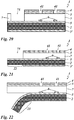
- antenna structures 52, 11 arranged in analogy thereto can also be used so as to realize an inductive coupling. Ideally, these are tuned so that the external transmit antenna 11 operates in resonance with the internal receive antenna 52.
- the basic construction is Fig. 19 shown.
- an alternating current is generated in the interconnect layer 5 via the inductive coupling, without having to be contacted directly.
- a rectification can also be done by means of suitable components.
- the resonance frequency and range can be adjusted.
- information or control commands can also be transmitted to the embedded electronics integrated on the carrier layer.
- the external antenna 52 can also be applied directly to the carrier layer 2 or attached after completion of the multi-layer body 1.
- Another possibility for direct contacting of the conductor layer 5 is that they do not completely enclose with plastic during the injection molding of the plastic layer 7.
- a recess 75 can be left open in the plastic layer 7, as in Fig. 20 shown, or the plastic layer 7 are not applied to the edge of the carrier layer 2, so that there is a protruding tab 22 of the carrier layer on which the conductor layer 5 can be contacted (see Fig. 21 ).
- a portion 23 of the carrier layer 2, on which the conductor track layer 5 extends are detached from the plastic layer 7.
- a corresponding release layer can be applied to the subregion 23 prior to injection molding.
- the release layer preferably consists of a wax, a siloxane polymer or a fluorine-containing polymer (eg Teflon®) and has a layer thickness of 10 nm to 5 ⁇ m, preferably of 100 nm to 1 ⁇ m.
Landscapes
- Engineering & Computer Science (AREA)
- Manufacturing & Machinery (AREA)
- Mechanical Engineering (AREA)
- Injection Moulding Of Plastics Or The Like (AREA)
- Optical Elements Other Than Lenses (AREA)
- Optical Filters (AREA)
- Diffracting Gratings Or Hologram Optical Elements (AREA)
- Non-Portable Lighting Devices Or Systems Thereof (AREA)
- Illuminated Signs And Luminous Advertising (AREA)
- Laminated Bodies (AREA)
Priority Applications (1)
| Application Number | Priority Date | Filing Date | Title |
|---|---|---|---|
| PL15720099T PL3140097T3 (pl) | 2014-05-09 | 2015-05-07 | Korpus wielowarstwowy i sposób jego wytwarzania |
Applications Claiming Priority (2)
| Application Number | Priority Date | Filing Date | Title |
|---|---|---|---|
| DE102014106585.9A DE102014106585A1 (de) | 2014-05-09 | 2014-05-09 | Mehrschichtkörper und Verfahren zu dessen Herstellung |
| PCT/EP2015/060029 WO2015169890A2 (de) | 2014-05-09 | 2015-05-07 | Mehrschichtkörper und verfahren zu dessen herstellung |
Publications (2)
| Publication Number | Publication Date |
|---|---|
| EP3140097A2 EP3140097A2 (de) | 2017-03-15 |
| EP3140097B1 true EP3140097B1 (de) | 2019-09-04 |
Family
ID=53039921
Family Applications (1)
| Application Number | Title | Priority Date | Filing Date |
|---|---|---|---|
| EP15720099.9A Active EP3140097B1 (de) | 2014-05-09 | 2015-05-07 | Mehrschichtkörper und verfahren zu dessen herstellung |
Country Status (9)
| Country | Link |
|---|---|
| US (1) | US10335987B2 (https=) |
| EP (1) | EP3140097B1 (https=) |
| JP (1) | JP6687219B2 (https=) |
| KR (1) | KR102314674B1 (https=) |
| CN (1) | CN106660241B (https=) |
| DE (1) | DE102014106585A1 (https=) |
| ES (1) | ES2748425T3 (https=) |
| PL (1) | PL3140097T3 (https=) |
| WO (1) | WO2015169890A2 (https=) |
Families Citing this family (42)
| Publication number | Priority date | Publication date | Assignee | Title |
|---|---|---|---|---|
| CN114686137B (zh) * | 2015-12-04 | 2025-04-15 | 雷恩哈德库兹基金两合公司 | 膜以及用于制造膜的方法 |
| CN115356802B (zh) * | 2016-04-13 | 2026-02-13 | 塔科图特科有限责任公司 | 用于电子设备的多层的组件以及建立该组件的方法 |
| EP4325264A3 (en) | 2016-04-13 | 2024-05-22 | TactoTek Oy | Illuminated multilayer structure with embedded light sources |
| US11292166B2 (en) * | 2017-04-07 | 2022-04-05 | Tactotek Oy | Method for manufacturing an electronic assembly and an electronic assembly |
| ES2693388A1 (es) * | 2017-06-09 | 2018-12-11 | Srg Global Liria, S.L | Molduras de apariencia metálica traslúcidas a la luz y enmascaradas para iluminación selectiva |
| US11511467B2 (en) * | 2017-09-19 | 2022-11-29 | Lumileds Llc | Light emitting device and manufacturing method thereof |
| DE202017005182U1 (de) | 2017-10-09 | 2017-12-19 | Gerhardi Kunststofftechnik Gmbh | Einteiliges und multifunktionales Lichtgehäuse |
| US10619808B2 (en) | 2017-10-18 | 2020-04-14 | Good Earth Lighting, Inc. | Flat panel ceiling light with quick-change covers |
| CN107799347B (zh) * | 2017-10-30 | 2019-03-15 | 武汉理工大学 | 一种模内注塑薄膜开关 |
| CN107632475B (zh) * | 2017-10-31 | 2020-11-03 | 武汉天马微电子有限公司 | 显示面板及显示装置 |
| DE102018207296B4 (de) * | 2018-05-09 | 2025-01-23 | Joysonquin Automotive Systems Gmbh | Verfahren zum herstellen eines dekorteils |
| DE102018123473A1 (de) * | 2018-09-24 | 2020-03-26 | Leonhard Kurz Stiftung & Co. Kg | Dekorfolie, Transferfolie, Verwendung einer Transferfolie, Verfahren zur Herstellung einer Transferfolie, Verfahren zum Dekorieren eines Kunststoffformteils sowie Kunststoffformteil |
| US11482650B2 (en) * | 2018-11-07 | 2022-10-25 | Seoul Viosys Co., Ltd. | Light emitting device including light shielding layer |
| US11271136B2 (en) * | 2018-11-07 | 2022-03-08 | Seoul Viosys Co., Ltd | Light emitting device |
| FR3093241B1 (fr) * | 2019-02-25 | 2021-04-09 | Plastic Omnium Cie | Dispositif de protection de radar rétro-éclairé |
| ES2799830A1 (es) * | 2019-06-17 | 2020-12-21 | Srg Global Liria S L | Electronica en molde y sus metodos de fabricacion |
| CN110450342B (zh) * | 2019-07-31 | 2022-02-08 | 汕头超声显示器技术有限公司 | 一种用于电容触摸屏的塑料件及其制作方法 |
| DE102019127108A1 (de) | 2019-10-09 | 2021-04-15 | Leonhard Kurz Stiftung & Co. Kg | Verfahren und Vorrichtung zur Herstellung eines Kunststoffbauteils sowie ein Kunststoffbauteil |
| CN111231217A (zh) * | 2020-01-21 | 2020-06-05 | 东莞广华汽车饰件科技有限公司 | 一种车用控制开关的制造工艺 |
| DE102020105361A1 (de) * | 2020-02-28 | 2021-09-02 | Leonhard Kurz Stiftung & Co. Kg | Verfahren und Vorrichtung zum Dekorieren eines Spritzgussformteils sowie ein Spritzgussformteil |
| DE102020113334A1 (de) * | 2020-05-18 | 2021-11-18 | Bayerische Motoren Werke Aktiengesellschaft | Pressträger mit partieller Hinterleuchtung |
| CN111923323A (zh) * | 2020-06-23 | 2020-11-13 | 苏州斯普兰蒂电子有限公司 | 一种内置led灯电路的模内注塑产品的制备工艺 |
| KR102357563B1 (ko) * | 2020-12-14 | 2022-02-07 | 인탑스 주식회사 | 전자회로 도금 공법을 이용한 ime 구조 및 그 제조방법 |
| DE102021104294A1 (de) * | 2021-02-23 | 2022-08-25 | Polyic Gmbh & Co. Kg | Schichtkörper mit Dekorationsschicht und Verfahren zur Herstellung |
| CN112959647A (zh) * | 2021-03-08 | 2021-06-15 | 东莞广华汽车饰件科技有限公司 | 一种内溅镀式胶膜汽车装饰件的制造方法 |
| CN112936735A (zh) * | 2021-03-08 | 2021-06-11 | 东莞广华汽车饰件科技有限公司 | 一种双色遮蔽内溅镀式车用发光装饰件的制造方法 |
| US11175438B1 (en) | 2021-05-17 | 2021-11-16 | Tactotek Oy | Optoelectronically functional multilayer structure having embedded light-defining segments and related manufacturing method |
| KR102950780B1 (ko) * | 2021-06-23 | 2026-04-09 | 삼성디스플레이 주식회사 | 표시 장치 및 그 제조방법 |
| KR102394587B1 (ko) * | 2021-07-19 | 2022-05-06 | 인탑스 주식회사 | 다중 ime 구조 및 그 제조 방법 |
| CN113696410A (zh) * | 2021-08-26 | 2021-11-26 | 东莞广华汽车饰件科技有限公司 | 一种具有发光功能的汽车装饰件的制造方法 |
| KR102916012B1 (ko) * | 2021-09-27 | 2026-01-22 | 삼성전자주식회사 | 디스플레이 모듈 및 이를 포함하는 웨어러블 전자 장치 |
| DE102021133016A1 (de) | 2021-12-14 | 2023-06-15 | Bayerische Motoren Werke Aktiengesellschaft | Fahrzeugbauteil, Fahrzeug und Herstellungsverfahren |
| DE102022202407A1 (de) | 2022-03-10 | 2023-09-14 | Faurecia Innenraum Systeme Gmbh | Fahrzeugverkleidungsteil |
| CN114347395B (zh) * | 2022-03-17 | 2022-06-03 | 威海嘉瑞光电科技股份有限公司 | 半导体光学器件的封装方法及其使用的装置 |
| JP7833142B2 (ja) * | 2022-03-23 | 2026-03-19 | スタンレー電気株式会社 | 波長変換装置及び照明装置 |
| FR3137321B1 (fr) * | 2022-06-29 | 2025-08-29 | Faurecia Interieur Ind | Procédé pour réaliser un dispositif électronique moulé et dispositif électronique moulé |
| CN115071321A (zh) * | 2022-07-09 | 2022-09-20 | 杨剑桥 | 多图案融合的透光装饰结构 |
| FR3144257B1 (fr) | 2022-12-23 | 2024-12-13 | Commissariat Energie Atomique | Système de rétro-éclairage d’un pictogramme lumineux à homogénéité d’éclairage améliorée |
| US20240322093A1 (en) * | 2023-03-23 | 2024-09-26 | Yenrich Technology Corporation | Light-emitting module |
| DE102023002623A1 (de) | 2023-06-28 | 2025-01-02 | Mercedes-Benz Group AG | Durchleuchtbares Bauteil, Fahrzeugstrukturbauteil mit demselben sowie Kraftfahrzeug |
| DE102024111943B3 (de) * | 2024-04-29 | 2025-07-31 | Bayerische Motoren Werke Aktiengesellschaft | Bauteil für einen Kraftwagen |
| US20260009905A1 (en) * | 2024-07-08 | 2026-01-08 | Htc Corporation | Optical tracking device |
Family Cites Families (21)
| Publication number | Priority date | Publication date | Assignee | Title |
|---|---|---|---|---|
| JPH0787263B2 (ja) * | 1987-06-23 | 1995-09-20 | 住友電気工業株式会社 | 補強型フレキシブル配線板の製造方法 |
| DE19717740C2 (de) * | 1997-04-26 | 2001-07-05 | Schoenberg & Cerny Gmbh Wien | Kunststoff-Formkörper mit integriertem optoelektronischem Leuchtfeld und Verfahren zu seiner Herstellung |
| DE19920627A1 (de) * | 1998-05-28 | 1999-12-02 | Merck Patent Gmbh | Pigmentmischung |
| DE10234125A1 (de) * | 2002-07-26 | 2004-02-12 | Siemens Ag | Beleuchtbares Kunststoffspritzgussteil mit einer Anzeigefunktion und Verfahren zu dessen Herstellung |
| DE10346452A1 (de) * | 2003-10-03 | 2005-04-28 | Schefenacker Vision Systems | Leuchtelement mit Einlegelichtleitkörper |
| DE102004041868B3 (de) * | 2004-08-27 | 2006-03-02 | Leonhard Kurz Gmbh & Co. Kg | Transferfolie, deren Verwendung sowie Verfahren zur Herstellung von dekorierten Kunststoffartikeln |
| JP4675096B2 (ja) * | 2004-12-06 | 2011-04-20 | 株式会社リコー | 三次元成形回路部品の製造方法およびこれにより製造された三次元成形回路部品 |
| DE102005023440A1 (de) * | 2005-05-20 | 2006-11-30 | BSH Bosch und Siemens Hausgeräte GmbH | Anzeige- und/oder Bedienungspaneel |
| US20100196651A1 (en) * | 2005-09-28 | 2010-08-05 | Sipix Chemical Inc. | Mold manufacturing of an object comprising a functional element, transfering process and object |
| US8092904B2 (en) * | 2006-03-31 | 2012-01-10 | 3M Innovative Properties Company | Optical article having an antistatic layer |
| US7811672B2 (en) * | 2007-01-30 | 2010-10-12 | Ult Technology Co., Ltd. | LED lampshade injection-molded or pressure cast with an IMD film |
| US8198979B2 (en) * | 2007-04-20 | 2012-06-12 | Ink-Logix, Llc | In-molded resistive and shielding elements |
| DE102009033762A1 (de) | 2009-07-17 | 2011-01-27 | Leonhard Kurz Stiftung & Co. Kg | Verfahren zur Herstellung eines Mehrschichtkörpers sowie Mehrschichtkörper |
| FI122621B (fi) * | 2009-08-20 | 2012-04-30 | Lite On Mobile Oyj | Elektroniikkalaite ja sen kuoriosa |
| WO2012049895A1 (ja) * | 2010-10-15 | 2012-04-19 | 日本電気株式会社 | 部品内蔵モジュール及びこれを備える電子機器並びに部品内蔵モジュールの製造方法 |
| EP2638321B1 (en) * | 2010-11-10 | 2019-05-08 | Nanosys, Inc. | Quantum dot films, lighting devices, and lighting methods |
| SI2525138T1 (sl) * | 2011-05-19 | 2014-04-30 | Odelo Gmbh | Luäś motornega vozila in postopek njene izdelave |
| US8804344B2 (en) * | 2011-06-10 | 2014-08-12 | Scott Moncrieff | Injection molded control panel with in-molded decorated plastic film |
| DE102011077896A1 (de) * | 2011-06-21 | 2012-12-27 | BSH Bosch und Siemens Hausgeräte GmbH | Bedien- und Anzeigeeinrichtung für ein Haushaltsgerät und Haushaltsgerät |
| JP6171291B2 (ja) * | 2012-09-07 | 2017-08-02 | 凸版印刷株式会社 | 表示体の真偽判定方法 |
| US9297675B2 (en) * | 2013-10-04 | 2016-03-29 | Tactotek Oy | Illuminated indicator structures for electronic devices |
-
2014
- 2014-05-09 DE DE102014106585.9A patent/DE102014106585A1/de not_active Ceased
-
2015
- 2015-05-07 US US15/309,074 patent/US10335987B2/en active Active
- 2015-05-07 CN CN201580034495.2A patent/CN106660241B/zh active Active
- 2015-05-07 ES ES15720099T patent/ES2748425T3/es active Active
- 2015-05-07 WO PCT/EP2015/060029 patent/WO2015169890A2/de not_active Ceased
- 2015-05-07 KR KR1020167034306A patent/KR102314674B1/ko active Active
- 2015-05-07 PL PL15720099T patent/PL3140097T3/pl unknown
- 2015-05-07 JP JP2016567185A patent/JP6687219B2/ja active Active
- 2015-05-07 EP EP15720099.9A patent/EP3140097B1/de active Active
Non-Patent Citations (1)
| Title |
|---|
| None * |
Also Published As
| Publication number | Publication date |
|---|---|
| US10335987B2 (en) | 2019-07-02 |
| JP6687219B2 (ja) | 2020-04-22 |
| PL3140097T3 (pl) | 2020-02-28 |
| KR102314674B1 (ko) | 2021-10-20 |
| JP2017522583A (ja) | 2017-08-10 |
| EP3140097A2 (de) | 2017-03-15 |
| WO2015169890A2 (de) | 2015-11-12 |
| KR20170026353A (ko) | 2017-03-08 |
| DE102014106585A1 (de) | 2015-11-12 |
| US20170066168A1 (en) | 2017-03-09 |
| WO2015169890A3 (de) | 2016-02-04 |
| ES2748425T3 (es) | 2020-03-16 |
| CN106660241A (zh) | 2017-05-10 |
| CN106660241B (zh) | 2019-08-16 |
Similar Documents
| Publication | Publication Date | Title |
|---|---|---|
| EP3140097B1 (de) | Mehrschichtkörper und verfahren zu dessen herstellung | |
| EP1911630B1 (de) | Baugruppe zur beleuchteten Darstellung eines Logos | |
| DE102011050585B4 (de) | Verfahren zur Herstellung eines Kunststoffformkörpers als Anzeige- und/oder Funktionselement und Kunststoffformkörper | |
| EP3856535B1 (de) | Dekorfolie, verfahren zum dekorieren eines kunststoffformteils sowie kunststoffformteil | |
| DE202016105622U1 (de) | Beleuchtete Plakette für ein Fahrzeug | |
| EP3150442B1 (de) | Zierteil für ein fahrzeug | |
| DE102014112470B4 (de) | Ausstattungsteil mit leuchtender sichtseite | |
| EP2803531B1 (de) | Flächige Vorrichtung zur Beleuchtung der Innenausstattung eines Fahrzeugs | |
| EP2942233B1 (de) | Flächiges beleuchtungselement für die innenausstattung eines fahrzeugs | |
| DE112020005121T5 (de) | Beleuchtete anzeigetafel und verfahren zur herstellung derselben | |
| DE112018005570B4 (de) | Formartikel, anzeigevorrichtung einschliesslich des formartikels und verfahren zur herstellung eines formartikels | |
| DE202016106848U1 (de) | Beleuchtete Verkleidungsbaugruppe | |
| DE102011102532B4 (de) | Verfahren zum Herstellen einer Abdeckung für eine Leuchteneinheit | |
| EP2525138B1 (de) | Kraftfahrzeugleuchte und Verfahren zu deren Herstellung | |
| DE102011117985B4 (de) | Kunstoffteil sowie Verfahren zur Herstellung eines Kunstoffteils | |
| DE202016103404U1 (de) | Beleuchtete Aussenleiste | |
| EP1514731A2 (de) | Fahrzeugleuchte | |
| DE102021113047A1 (de) | Anzeigeelement und verfahren | |
| DE102004012467A1 (de) | Fahrzeug-Folienbauteil und Verfahren zu dessen Herstellung | |
| WO2024217954A1 (de) | Verfahren und vorrichtung zur herstellung eines folienkörpers, folienkörper, verfarhen zur herstellung eines schichtverbunds, schichtverbund, verfahren zur herstellung eines heizfolien-verbunds, heizfolien-verbund und vorrichtung | |
| WO2016042417A1 (de) | Verfahren zur herstellung einer bestückt umformbaren, hinterspritzbaren schaltungsträgereinheit, sowie schaltungsträgereinheit | |
| EP2201414B1 (de) | Leuchtobjekt | |
| DE102023109577A1 (de) | Verfahren und Vorrichtung zur Herstellung eines Folienkörpers, Folienkörper, Verfahren zur Herstellung eines Schichtverbunds, Schichtverbund und Vorrichtung | |
| DE102021119768A1 (de) | Verkleidungsteil und produkt mit einem verkleidungsteil | |
| DE102006030494B4 (de) | Betätigungseinrichtung mit einem Schichtaufbau, der einen Piezoschaltaufbau und eine Leuchtebene enthält |
Legal Events
| Date | Code | Title | Description |
|---|---|---|---|
| STAA | Information on the status of an ep patent application or granted ep patent |
Free format text: STATUS: THE INTERNATIONAL PUBLICATION HAS BEEN MADE |
|
| PUAI | Public reference made under article 153(3) epc to a published international application that has entered the european phase |
Free format text: ORIGINAL CODE: 0009012 |
|
| STAA | Information on the status of an ep patent application or granted ep patent |
Free format text: STATUS: REQUEST FOR EXAMINATION WAS MADE |
|
| 17P | Request for examination filed |
Effective date: 20161104 |
|
| AK | Designated contracting states |
Kind code of ref document: A2 Designated state(s): AL AT BE BG CH CY CZ DE DK EE ES FI FR GB GR HR HU IE IS IT LI LT LU LV MC MK MT NL NO PL PT RO RS SE SI SK SM TR |
|
| AX | Request for extension of the european patent |
Extension state: BA ME |
|
| DAV | Request for validation of the european patent (deleted) | ||
| DAX | Request for extension of the european patent (deleted) | ||
| STAA | Information on the status of an ep patent application or granted ep patent |
Free format text: STATUS: EXAMINATION IS IN PROGRESS |
|
| 17Q | First examination report despatched |
Effective date: 20181115 |
|
| GRAP | Despatch of communication of intention to grant a patent |
Free format text: ORIGINAL CODE: EPIDOSNIGR1 |
|
| STAA | Information on the status of an ep patent application or granted ep patent |
Free format text: STATUS: GRANT OF PATENT IS INTENDED |
|
| INTG | Intention to grant announced |
Effective date: 20190513 |
|
| GRAS | Grant fee paid |
Free format text: ORIGINAL CODE: EPIDOSNIGR3 |
|
| GRAA | (expected) grant |
Free format text: ORIGINAL CODE: 0009210 |
|
| STAA | Information on the status of an ep patent application or granted ep patent |
Free format text: STATUS: THE PATENT HAS BEEN GRANTED |
|
| AK | Designated contracting states |
Kind code of ref document: B1 Designated state(s): AL AT BE BG CH CY CZ DE DK EE ES FI FR GB GR HR HU IE IS IT LI LT LU LV MC MK MT NL NO PL PT RO RS SE SI SK SM TR |
|
| REG | Reference to a national code |
Ref country code: GB Ref legal event code: FG4D Free format text: NOT ENGLISH |
|
| REG | Reference to a national code |
Ref country code: CH Ref legal event code: EP Ref country code: CH Ref legal event code: NV Representative=s name: FIAMMENGHI-FIAMMENGHI, CH |
|
| REG | Reference to a national code |
Ref country code: AT Ref legal event code: REF Ref document number: 1174742 Country of ref document: AT Kind code of ref document: T Effective date: 20190915 |
|
| REG | Reference to a national code |
Ref country code: DE Ref legal event code: R096 Ref document number: 502015010241 Country of ref document: DE |
|
| REG | Reference to a national code |
Ref country code: IE Ref legal event code: FG4D Free format text: LANGUAGE OF EP DOCUMENT: GERMAN |
|
| REG | Reference to a national code |
Ref country code: NL Ref legal event code: FP |
|
| REG | Reference to a national code |
Ref country code: RO Ref legal event code: EPE |
|
| REG | Reference to a national code |
Ref country code: SE Ref legal event code: TRGR |
|
| REG | Reference to a national code |
Ref country code: LT Ref legal event code: MG4D |
|
| PG25 | Lapsed in a contracting state [announced via postgrant information from national office to epo] |
Ref country code: NO Free format text: LAPSE BECAUSE OF FAILURE TO SUBMIT A TRANSLATION OF THE DESCRIPTION OR TO PAY THE FEE WITHIN THE PRESCRIBED TIME-LIMIT Effective date: 20191204 Ref country code: LT Free format text: LAPSE BECAUSE OF FAILURE TO SUBMIT A TRANSLATION OF THE DESCRIPTION OR TO PAY THE FEE WITHIN THE PRESCRIBED TIME-LIMIT Effective date: 20190904 Ref country code: FI Free format text: LAPSE BECAUSE OF FAILURE TO SUBMIT A TRANSLATION OF THE DESCRIPTION OR TO PAY THE FEE WITHIN THE PRESCRIBED TIME-LIMIT Effective date: 20190904 Ref country code: HR Free format text: LAPSE BECAUSE OF FAILURE TO SUBMIT A TRANSLATION OF THE DESCRIPTION OR TO PAY THE FEE WITHIN THE PRESCRIBED TIME-LIMIT Effective date: 20190904 Ref country code: BG Free format text: LAPSE BECAUSE OF FAILURE TO SUBMIT A TRANSLATION OF THE DESCRIPTION OR TO PAY THE FEE WITHIN THE PRESCRIBED TIME-LIMIT Effective date: 20191204 |
|
| PG25 | Lapsed in a contracting state [announced via postgrant information from national office to epo] |
Ref country code: AL Free format text: LAPSE BECAUSE OF FAILURE TO SUBMIT A TRANSLATION OF THE DESCRIPTION OR TO PAY THE FEE WITHIN THE PRESCRIBED TIME-LIMIT Effective date: 20190904 Ref country code: LV Free format text: LAPSE BECAUSE OF FAILURE TO SUBMIT A TRANSLATION OF THE DESCRIPTION OR TO PAY THE FEE WITHIN THE PRESCRIBED TIME-LIMIT Effective date: 20190904 Ref country code: RS Free format text: LAPSE BECAUSE OF FAILURE TO SUBMIT A TRANSLATION OF THE DESCRIPTION OR TO PAY THE FEE WITHIN THE PRESCRIBED TIME-LIMIT Effective date: 20190904 Ref country code: GR Free format text: LAPSE BECAUSE OF FAILURE TO SUBMIT A TRANSLATION OF THE DESCRIPTION OR TO PAY THE FEE WITHIN THE PRESCRIBED TIME-LIMIT Effective date: 20191205 |
|
| REG | Reference to a national code |
Ref country code: ES Ref legal event code: FG2A Ref document number: 2748425 Country of ref document: ES Kind code of ref document: T3 Effective date: 20200316 |
|
| PG25 | Lapsed in a contracting state [announced via postgrant information from national office to epo] |
Ref country code: PT Free format text: LAPSE BECAUSE OF FAILURE TO SUBMIT A TRANSLATION OF THE DESCRIPTION OR TO PAY THE FEE WITHIN THE PRESCRIBED TIME-LIMIT Effective date: 20200106 Ref country code: EE Free format text: LAPSE BECAUSE OF FAILURE TO SUBMIT A TRANSLATION OF THE DESCRIPTION OR TO PAY THE FEE WITHIN THE PRESCRIBED TIME-LIMIT Effective date: 20190904 |
|
| PG25 | Lapsed in a contracting state [announced via postgrant information from national office to epo] |
Ref country code: CZ Free format text: LAPSE BECAUSE OF FAILURE TO SUBMIT A TRANSLATION OF THE DESCRIPTION OR TO PAY THE FEE WITHIN THE PRESCRIBED TIME-LIMIT Effective date: 20190904 Ref country code: IS Free format text: LAPSE BECAUSE OF FAILURE TO SUBMIT A TRANSLATION OF THE DESCRIPTION OR TO PAY THE FEE WITHIN THE PRESCRIBED TIME-LIMIT Effective date: 20200224 Ref country code: SM Free format text: LAPSE BECAUSE OF FAILURE TO SUBMIT A TRANSLATION OF THE DESCRIPTION OR TO PAY THE FEE WITHIN THE PRESCRIBED TIME-LIMIT Effective date: 20190904 Ref country code: SK Free format text: LAPSE BECAUSE OF FAILURE TO SUBMIT A TRANSLATION OF THE DESCRIPTION OR TO PAY THE FEE WITHIN THE PRESCRIBED TIME-LIMIT Effective date: 20190904 |
|
| REG | Reference to a national code |
Ref country code: DE Ref legal event code: R097 Ref document number: 502015010241 Country of ref document: DE |
|
| PLBE | No opposition filed within time limit |
Free format text: ORIGINAL CODE: 0009261 |
|
| STAA | Information on the status of an ep patent application or granted ep patent |
Free format text: STATUS: NO OPPOSITION FILED WITHIN TIME LIMIT |
|
| PG2D | Information on lapse in contracting state deleted |
Ref country code: IS |
|
| PG25 | Lapsed in a contracting state [announced via postgrant information from national office to epo] |
Ref country code: DK Free format text: LAPSE BECAUSE OF FAILURE TO SUBMIT A TRANSLATION OF THE DESCRIPTION OR TO PAY THE FEE WITHIN THE PRESCRIBED TIME-LIMIT Effective date: 20190904 Ref country code: IS Free format text: LAPSE BECAUSE OF FAILURE TO SUBMIT A TRANSLATION OF THE DESCRIPTION OR TO PAY THE FEE WITHIN THE PRESCRIBED TIME-LIMIT Effective date: 20200105 |
|
| 26N | No opposition filed |
Effective date: 20200605 |
|
| PG25 | Lapsed in a contracting state [announced via postgrant information from national office to epo] |
Ref country code: SI Free format text: LAPSE BECAUSE OF FAILURE TO SUBMIT A TRANSLATION OF THE DESCRIPTION OR TO PAY THE FEE WITHIN THE PRESCRIBED TIME-LIMIT Effective date: 20190904 |
|
| PG25 | Lapsed in a contracting state [announced via postgrant information from national office to epo] |
Ref country code: MC Free format text: LAPSE BECAUSE OF FAILURE TO SUBMIT A TRANSLATION OF THE DESCRIPTION OR TO PAY THE FEE WITHIN THE PRESCRIBED TIME-LIMIT Effective date: 20190904 |
|
| REG | Reference to a national code |
Ref country code: BE Ref legal event code: MM Effective date: 20200531 |
|
| PG25 | Lapsed in a contracting state [announced via postgrant information from national office to epo] |
Ref country code: LU Free format text: LAPSE BECAUSE OF NON-PAYMENT OF DUE FEES Effective date: 20200507 |
|
| PG25 | Lapsed in a contracting state [announced via postgrant information from national office to epo] |
Ref country code: IE Free format text: LAPSE BECAUSE OF NON-PAYMENT OF DUE FEES Effective date: 20200507 |
|
| PG25 | Lapsed in a contracting state [announced via postgrant information from national office to epo] |
Ref country code: BE Free format text: LAPSE BECAUSE OF NON-PAYMENT OF DUE FEES Effective date: 20200531 |
|
| PG25 | Lapsed in a contracting state [announced via postgrant information from national office to epo] |
Ref country code: MT Free format text: LAPSE BECAUSE OF FAILURE TO SUBMIT A TRANSLATION OF THE DESCRIPTION OR TO PAY THE FEE WITHIN THE PRESCRIBED TIME-LIMIT Effective date: 20190904 Ref country code: CY Free format text: LAPSE BECAUSE OF FAILURE TO SUBMIT A TRANSLATION OF THE DESCRIPTION OR TO PAY THE FEE WITHIN THE PRESCRIBED TIME-LIMIT Effective date: 20190904 |
|
| PG25 | Lapsed in a contracting state [announced via postgrant information from national office to epo] |
Ref country code: MK Free format text: LAPSE BECAUSE OF FAILURE TO SUBMIT A TRANSLATION OF THE DESCRIPTION OR TO PAY THE FEE WITHIN THE PRESCRIBED TIME-LIMIT Effective date: 20190904 |
|
| PGFP | Annual fee paid to national office [announced via postgrant information from national office to epo] |
Ref country code: NL Payment date: 20250522 Year of fee payment: 11 |
|
| PGFP | Annual fee paid to national office [announced via postgrant information from national office to epo] |
Ref country code: DE Payment date: 20250505 Year of fee payment: 11 |
|
| PGFP | Annual fee paid to national office [announced via postgrant information from national office to epo] |
Ref country code: ES Payment date: 20250616 Year of fee payment: 11 |
|
| PGFP | Annual fee paid to national office [announced via postgrant information from national office to epo] |
Ref country code: IT Payment date: 20250530 Year of fee payment: 11 |
|
| PGFP | Annual fee paid to national office [announced via postgrant information from national office to epo] |
Ref country code: FR Payment date: 20250523 Year of fee payment: 11 |
|
| PGFP | Annual fee paid to national office [announced via postgrant information from national office to epo] |
Ref country code: CH Payment date: 20250601 Year of fee payment: 11 |
|
| PGFP | Annual fee paid to national office [announced via postgrant information from national office to epo] |
Ref country code: RO Payment date: 20250430 Year of fee payment: 11 Ref country code: AT Payment date: 20250519 Year of fee payment: 11 |
|
| PGFP | Annual fee paid to national office [announced via postgrant information from national office to epo] |
Ref country code: TR Payment date: 20250430 Year of fee payment: 11 |
|
| PGFP | Annual fee paid to national office [announced via postgrant information from national office to epo] |
Ref country code: SE Payment date: 20250522 Year of fee payment: 11 |
|
| PGFP | Annual fee paid to national office [announced via postgrant information from national office to epo] |
Ref country code: GB Payment date: 20260324 Year of fee payment: 12 |
|
| PGFP | Annual fee paid to national office [announced via postgrant information from national office to epo] |
Ref country code: PL Payment date: 20260319 Year of fee payment: 12 |