EP3140097B1 - Multilayer body and method for producing same - Google Patents
Multilayer body and method for producing same Download PDFInfo
- Publication number
- EP3140097B1 EP3140097B1 EP15720099.9A EP15720099A EP3140097B1 EP 3140097 B1 EP3140097 B1 EP 3140097B1 EP 15720099 A EP15720099 A EP 15720099A EP 3140097 B1 EP3140097 B1 EP 3140097B1
- Authority
- EP
- European Patent Office
- Prior art keywords
- ply
- layer
- carrier
- plastic
- illuminant
- Prior art date
- Legal status (The legal status is an assumption and is not a legal conclusion. Google has not performed a legal analysis and makes no representation as to the accuracy of the status listed.)
- Active
Links
Images


Classifications
-
- B—PERFORMING OPERATIONS; TRANSPORTING
- B29—WORKING OF PLASTICS; WORKING OF SUBSTANCES IN A PLASTIC STATE IN GENERAL
- B29C—SHAPING OR JOINING OF PLASTICS; SHAPING OF MATERIAL IN A PLASTIC STATE, NOT OTHERWISE PROVIDED FOR; AFTER-TREATMENT OF THE SHAPED PRODUCTS, e.g. REPAIRING
- B29C45/00—Injection moulding, i.e. forcing the required volume of moulding material through a nozzle into a closed mould; Apparatus therefor
- B29C45/14—Injection moulding, i.e. forcing the required volume of moulding material through a nozzle into a closed mould; Apparatus therefor incorporating preformed parts or layers, e.g. injection moulding around inserts or for coating articles
- B29C45/14778—Injection moulding, i.e. forcing the required volume of moulding material through a nozzle into a closed mould; Apparatus therefor incorporating preformed parts or layers, e.g. injection moulding around inserts or for coating articles the article consisting of a material with particular properties, e.g. porous, brittle
- B29C45/14811—Multilayered articles
-
- B—PERFORMING OPERATIONS; TRANSPORTING
- B29—WORKING OF PLASTICS; WORKING OF SUBSTANCES IN A PLASTIC STATE IN GENERAL
- B29C—SHAPING OR JOINING OF PLASTICS; SHAPING OF MATERIAL IN A PLASTIC STATE, NOT OTHERWISE PROVIDED FOR; AFTER-TREATMENT OF THE SHAPED PRODUCTS, e.g. REPAIRING
- B29C45/00—Injection moulding, i.e. forcing the required volume of moulding material through a nozzle into a closed mould; Apparatus therefor
- B29C45/14—Injection moulding, i.e. forcing the required volume of moulding material through a nozzle into a closed mould; Apparatus therefor incorporating preformed parts or layers, e.g. injection moulding around inserts or for coating articles
- B29C45/14639—Injection moulding, i.e. forcing the required volume of moulding material through a nozzle into a closed mould; Apparatus therefor incorporating preformed parts or layers, e.g. injection moulding around inserts or for coating articles for obtaining an insulating effect, e.g. for electrical components
- B29C45/14655—Injection moulding, i.e. forcing the required volume of moulding material through a nozzle into a closed mould; Apparatus therefor incorporating preformed parts or layers, e.g. injection moulding around inserts or for coating articles for obtaining an insulating effect, e.g. for electrical components connected to or mounted on a carrier, e.g. lead frame
-
- B—PERFORMING OPERATIONS; TRANSPORTING
- B29—WORKING OF PLASTICS; WORKING OF SUBSTANCES IN A PLASTIC STATE IN GENERAL
- B29C—SHAPING OR JOINING OF PLASTICS; SHAPING OF MATERIAL IN A PLASTIC STATE, NOT OTHERWISE PROVIDED FOR; AFTER-TREATMENT OF THE SHAPED PRODUCTS, e.g. REPAIRING
- B29C45/00—Injection moulding, i.e. forcing the required volume of moulding material through a nozzle into a closed mould; Apparatus therefor
- B29C45/14—Injection moulding, i.e. forcing the required volume of moulding material through a nozzle into a closed mould; Apparatus therefor incorporating preformed parts or layers, e.g. injection moulding around inserts or for coating articles
- B29C45/14688—Coating articles provided with a decoration
-
- H—ELECTRICITY
- H01—ELECTRIC ELEMENTS
- H01L—SEMICONDUCTOR DEVICES NOT COVERED BY CLASS H10
- H01L25/00—Assemblies consisting of a plurality of individual semiconductor or other solid state devices ; Multistep manufacturing processes thereof
- H01L25/03—Assemblies consisting of a plurality of individual semiconductor or other solid state devices ; Multistep manufacturing processes thereof all the devices being of a type provided for in the same subgroup of groups H01L27/00 - H01L33/00, or in a single subclass of H10K, H10N, e.g. assemblies of rectifier diodes
- H01L25/04—Assemblies consisting of a plurality of individual semiconductor or other solid state devices ; Multistep manufacturing processes thereof all the devices being of a type provided for in the same subgroup of groups H01L27/00 - H01L33/00, or in a single subclass of H10K, H10N, e.g. assemblies of rectifier diodes the devices not having separate containers
- H01L25/075—Assemblies consisting of a plurality of individual semiconductor or other solid state devices ; Multistep manufacturing processes thereof all the devices being of a type provided for in the same subgroup of groups H01L27/00 - H01L33/00, or in a single subclass of H10K, H10N, e.g. assemblies of rectifier diodes the devices not having separate containers the devices being of a type provided for in group H01L33/00
- H01L25/0753—Assemblies consisting of a plurality of individual semiconductor or other solid state devices ; Multistep manufacturing processes thereof all the devices being of a type provided for in the same subgroup of groups H01L27/00 - H01L33/00, or in a single subclass of H10K, H10N, e.g. assemblies of rectifier diodes the devices not having separate containers the devices being of a type provided for in group H01L33/00 the devices being arranged next to each other
-
- H—ELECTRICITY
- H01—ELECTRIC ELEMENTS
- H01L—SEMICONDUCTOR DEVICES NOT COVERED BY CLASS H10
- H01L33/00—Semiconductor devices with at least one potential-jump barrier or surface barrier specially adapted for light emission; Processes or apparatus specially adapted for the manufacture or treatment thereof or of parts thereof; Details thereof
- H01L33/48—Semiconductor devices with at least one potential-jump barrier or surface barrier specially adapted for light emission; Processes or apparatus specially adapted for the manufacture or treatment thereof or of parts thereof; Details thereof characterised by the semiconductor body packages
- H01L33/58—Optical field-shaping elements
-
- B—PERFORMING OPERATIONS; TRANSPORTING
- B29—WORKING OF PLASTICS; WORKING OF SUBSTANCES IN A PLASTIC STATE IN GENERAL
- B29L—INDEXING SCHEME ASSOCIATED WITH SUBCLASS B29C, RELATING TO PARTICULAR ARTICLES
- B29L2009/00—Layered products
-
- B—PERFORMING OPERATIONS; TRANSPORTING
- B29—WORKING OF PLASTICS; WORKING OF SUBSTANCES IN A PLASTIC STATE IN GENERAL
- B29L—INDEXING SCHEME ASSOCIATED WITH SUBCLASS B29C, RELATING TO PARTICULAR ARTICLES
- B29L2031/00—Other particular articles
- B29L2031/34—Electrical apparatus, e.g. sparking plugs or parts thereof
- B29L2031/3493—Moulded interconnect devices, i.e. moulded articles provided with integrated circuit traces
-
- H—ELECTRICITY
- H01—ELECTRIC ELEMENTS
- H01L—SEMICONDUCTOR DEVICES NOT COVERED BY CLASS H10
- H01L2924/00—Indexing scheme for arrangements or methods for connecting or disconnecting semiconductor or solid-state bodies as covered by H01L24/00
-
- H—ELECTRICITY
- H01—ELECTRIC ELEMENTS
- H01L—SEMICONDUCTOR DEVICES NOT COVERED BY CLASS H10
- H01L2924/00—Indexing scheme for arrangements or methods for connecting or disconnecting semiconductor or solid-state bodies as covered by H01L24/00
- H01L2924/0001—Technical content checked by a classifier
- H01L2924/0002—Not covered by any one of groups H01L24/00, H01L24/00 and H01L2224/00
-
- H—ELECTRICITY
- H01—ELECTRIC ELEMENTS
- H01L—SEMICONDUCTOR DEVICES NOT COVERED BY CLASS H10
- H01L2933/00—Details relating to devices covered by the group H01L33/00 but not provided for in its subgroups
- H01L2933/0008—Processes
- H01L2933/0033—Processes relating to semiconductor body packages
- H01L2933/0058—Processes relating to semiconductor body packages relating to optical field-shaping elements
Definitions
- the invention relates to a method for producing a multilayer body and to a multilayer body produced in this way.
- plastic parts In the manufacture of plastic components is increasingly required in addition to a decoration and the integration of electronic functions. For example, plastic parts have long been provided with lighting elements to alert the user to a particular device condition (e.g., automotive trim elements, home appliance control panels).
- a particular device condition e.g., automotive trim elements, home appliance control panels.
- the already decorated plastic part must be connected in an additional manufacturing step with a conventional board that carries lighting elements, such as light emitting diodes, and / or other electronic components.
- additional layers between the plastic diaphragm and the light-emitting element must be installed in further manufacturing steps, which, for example, transform a point light source such as a light-emitting diode into a surface radiator (diffuser foils in the form of an additional light source Layer) or direct the light to different positions (optical fiber in the form of an additional layer).
- the LED board must also be connected by plug connections to a motherboard or a controller of the device.
- the US 2008/0180957 A1 discloses, for example, an LED board, which is connected to an already decorated injection molded part.
- the WO 2011/006634 A2 discloses a method for producing a multilayer body with a carrier layer and a one or multilayer decorative layer formed on and / or in the carrier layer, and a multi-layer body obtainable thereafter.
- the document XP055204300 discloses a self-luminous lateral boundary for trucks.
- the DE 197 17 740 A1 discloses plastic moldings with a graphically designed surface and integrated electroluminescent elements.
- the object of the present invention is therefore to provide a particularly simple and cost-effective method for producing a multilayer body with integrated decor and electronic functions, as well as such a multilayer body.
- a "layer” is to be understood as a preferably substantially flat structure, which in turn may itself consist of several layers. It may be, for example, a film or a board. Alternatively, however, more complex three-dimensional geometries are possible, especially for the plastic layer produced by injection molding.
- Such a layer need not necessarily represent an independent component, for example, a decorative layer can also be formed by printing on a substrate.
- connection of decorative layer, carrier layer and plastic layer can thus be done in a single step.
- a subsequent assembly of electronic components is not necessary, so that the production of a multi-layer body with integrated decor and integrated lighting in this way is particularly simple and inexpensive.
- a particularly stable and durable multi-layer body is created, the layers of which can be arranged reliably in a defined positional relationship.
- the decorative layer is applied to the carrier layer. This can be done before the injection molding of the plastic layer, so that the decorative layer and carrier layer are back-injected together or. However, it is also possible to apply the decorative layer only after the injection molding, for example by laminating a film or by printing on the composite of carrier and plastic layer. Carrier and decorative layer can also be placed together in the injection mold, so that they are in direct contact and connected during injection molding. For this purpose, one of the layers, for example, with a heat-activated Adhesive, which is activated under the pressure and temperature conditions of the injection molding process.
- the decorative layer is applied to the side facing away from the at least one light source side of the carrier layer.
- the light of the at least one light source then passes both through the carrier layer and through the decorative layer.
- the carrier layer itself can thus also serve as a coloring layer, as a diffuser or as a similar optical element.
- the decorative layer can also be applied to the side of the carrier layer facing the at least one luminous means, in particular between the luminous means and the carrier layer. As a result, a shorter beam path for the exiting light is realized, so that lower absorption losses occur.
- the carrier layer can also be made detachable, so that it can be removed after the back molding. Only the lighting means and the decorative layer, as well as possibly further functional elements such as strip conductors or the like on the plastic layer then remain.
- the decorative layer and the carrier layer are fixed in a mold half of the injection mold, in particular by mechanical clamping means and / or vacuum, and injected behind on one side.
- the injection molding can be done on the side of the decorative layer or the carrier layer. It is advantageous if the non-back-injected layer is applied flat against a wall of the injection molding tool, so that this position reliably does not come into contact with the plastic mass.
- plastic layer prefferably injection-molded between the side of the carrier layer facing away from the at least one luminous means and the decorative layer.
- the plastic layer can also be injection-molded between the side of the carrier layer facing the at least one luminous means and the decorative layer.
- Carrier and decorative layer are inserted, for example, in the respective opposite halves of an injection mold, without being in direct contact and the plastic layer injected into the space between the carrier and decorative layer.
- both the carrier and the decorative layer can be provided with a heat-activatable adhesive, which is activated under the pressure and temperature conditions of the injection molding process.
- the decorative layer is fixed in a first mold half of the injection mold and the carrier layer in a second mold half of the injection mold, in particular by mechanical clamping means and / or by vacuum.
- the respective layers are in turn applied flatly to an inner wall of the molding tool, so that they only come into contact with the plastic compound on one side.
- the decorative layer has a layer thickness of 0.1 .mu.m to 50 .mu.m, preferably from 1 .mu.m to 20 .mu.m.
- the decorative layer can be provided as an independent element, for example in the form of a film, which in turn can have several layers, for example printing or lacquer layers.
- the decorative layer can be provided by printing, in particular by pouring, screen printing, gravure or pad printing, and / or by coating on the carrier layer and / or the plastic layer.
- the carrier layer is preferably used as a film, in particular made of PET (polyethylene), PEN (polyethylene naphthalate), PC (polycarbonate), PVC (polyvinyl chloride), Kapton® (polyoxydiphenylenepyromellitimide) or other polyimides, PLA (polylactate), PMMA (polymethyl methacrylate ) or ABS (acrylonitrile butadiene styrene), with a layer thickness of 1 .mu.m to 500 .mu.m, preferably from 20 .mu.m to 300 .mu.m.
- PET polyethylene
- PEN polyethylene naphthalate
- PC polycarbonate
- PVC polyvinyl chloride
- Kapton® polyoxydiphenylenepyromellitimide
- PLA polylactate
- PMMA polymethyl methacrylate
- ABS acrylonitrile butadiene styrene
- the carrier layer can be provided as a printed circuit board, in particular made of FR4 (glass fiber fabric in epoxy resin matrix), polyimide or paper, with a layer thickness of 50 ⁇ m to 2 mm, preferably 100 ⁇ m to 1.5 mm.
- FR4 glass fiber fabric in epoxy resin matrix
- polyimide or paper with a layer thickness of 50 ⁇ m to 2 mm, preferably 100 ⁇ m to 1.5 mm.
- plastic compound of PMMA polymethyl methacrylate
- ABS acrylonitrile butadiene styrene
- PS polystyrene
- PE polyethylene
- PP polypropylene
- PC polycarbonate
- POM polyoxymethylene
- PA polyamide
- ASA acrylonitrile styrene acrylate
- SAN styrene-acrylonitrile
- TPU thermoplastic polyurethane
- the material properties of the multilayer body can be varied over a wide range depending on the desired field of use.
- the injection molding of the plastic layer in a pre-tempered tool at a melt temperature of 150 ° C to 350 ° C, preferably from 200 ° C to 300 ° C and / or a pressure of 500 bar to 2800 bar, preferably from 700 bar to 2500 bar carried out.
- an injection molding tool is used for injection molding of the plastic layer, which has a cavity with at least two partially planar and parallel inner walls. If the carrier layer and the decorative layer are applied to one or both of these inner walls prior to the injection molding of the plastic layer, then a laminar multi-layer body can be obtained.
- an injection molding tool can be used for injection molding of the plastic layer, which has a cavity with at least one partially curved inner wall.
- multi-layer bodies with more complex three-dimensional geometries can be obtained.
- the curvature can also be present only partially. It is also possible to further influence the geometry of the multilayer body through the use of sliders and / or cores within the cavity. Overall, all the usual design options known from injection molding are available here.
- SMD LEDs Surface Mounted Device
- SMD Surface Mounted Device
- / or chip LEDs having a length of 100 microns to 2 mm, preferably from 0 , 2 mm to 0.5 mm, a width of 100 microns to 2 mm, preferably from 0.2 mm to 0.5 mm, and a height of 50 microns to 250 microns, preferably from 75 microns to 125 microns, are used ,
- OLED organic light emitting diodes
- LOC light emitting cells
- electroluminescent displays can also be used as alternative light sources.
- additional components such as e.g. Logic circuits, resistors, diodes, piezo loudspeakers that are interconnected with the lighting elements are integrated.
- the light-emitting elements are used inter alia for the display of information states, alternatively or additionally, reflective, not self-luminous display elements can be integrated on the support, such. electrophoretic or electrochromic displays.
- At least one optical auxiliary layer in particular a reflection layer or absorption layer, is applied to the decorative layer and / or the carrier layer and / or the molded-on plastic layer.
- the light guide can be controlled within the multilayer body. It is possible, for example, to ensure only one-sided light emission or to avoid disturbing scattered light.
- Such auxiliary layers can also be applied only partially and thus provide, for example, defined outlet opening for the light of the at least one luminous means.
- the at least one auxiliary optical layer by vapor deposition or sputtering of a metal, in particular aluminum, silver, chromium, copper, gold, or alloys thereof with a layer thickness of 1 nm to 500 nm, preferably from 5 nm 100 nm, is generated.
- the reflective layer can also be produced by printing lacquers containing metal pigments having a layer thickness of from 0.1 ⁇ m to 50 ⁇ m, preferably from 1 ⁇ m to 20 ⁇ m.
- the at least one auxiliary optical layer is produced by applying a pigmented lacquer, in particular comprising carbon black pigments, with a layer thickness of 0.1 ⁇ m to 50 ⁇ m, preferably of 1 ⁇ m to 20 ⁇ m.
- the provided decorative layer is at least a first region which is at least partially transparent with respect to the spectrum of the light emitted by the at least one luminous means, and at least one second region which is non-transparent with respect to the spectrum of the light emitted by the at least one luminous means. ie is opaque.
- the first and second areas can form simple display areas or even complex optical information.
- the decorative layer is arranged so that the at least one lamp perpendicular to the surface of the decorative layer seen in overlapping with the at least one first area.
- the decorative layer can be arranged so that the at least one lamp perpendicular to the surface of the decorative layer seen in overlap with the at least one second area.
- colorants in particular dyes and / or pigments and / or particles and / or quantum dot materials and / or phosphorescent materials, which are in the wavelength range, are added to the plastic material used for injection molding of the plastic layer and / or to a layer of the carrier layer absorb and / or scatter the light emitted by the at least one light source and / or are excitable for fluorescence or phosphorescence in the visible wavelength range.
- the spectrum of the light emitted by the at least one luminous means can hereby be specifically influenced, in particular when using fluorescent or absorbing substances or quantum dots, so that a variety of color effects can be created.
- the added colorants comprise inorganic pigments and / or particles, in particular of silicon dioxide, fumed silica, titanium dioxide, zinc sulfide or a metal, with a particle size of 5 nm to 500 ⁇ m, preferably of 500 nm to 100 ⁇ m.
- a surface of the carrier layer is matted.
- a decorative layer which has a plurality of regions which differ in color and / or transparency with respect to the spectrum of the light emitted by the at least one luminous means.
- multi-colored graphic elements can be displayed whose appearance does not depend directly on the color of the lamps used. It is particularly useful when such a decorative layer is applied flat, so has no outlet openings. In addition, it is possible to realize decorations in this way, which are not visible in the off state of the at least one light source.
- a partial, with respect to the spectrum of the light emitted by the at least one light source light non-transparent layer, in particular a metal layer is applied to the decorative layer, which comprises optical information.
- an optically active relief structure in particular a diffractive structure, a zero-order diffraction structure, a macrostructure, a lens structure, a microlens structure, a microprism structure
- an optically active relief structure in particular a diffractive structure, a zero-order diffraction structure, a macrostructure, a lens structure, a microlens structure, a microprism structure
- the die can be integrally connected to the respective mold half or alternatively be designed as a separate insert or insert.
- the light output from the multi-layer body can also be controlled specifically.
- the decoupling of the light emitted by the light source can be selectively supported or prevented in regions.
- plastic masses are used in the injection molding of the plastic layer, which differ in an optical property, in particular in their optical refractive index.
- the casting of the different plastic masses can be carried out sequentially in different injection molding tools.
- the geometry of an injection molding tool for the sequential casting steps can be changed, for example by suitable slide.
- the positioning of the plastic or carrier layers on a turntable, which approaches different tool inserts for the sequential casting steps is possible.
- lens effects can be achieved in particular by refraction or mirror surfaces can be created by total reflection at the interfaces.
- a conductor track layer for contacting the at least one light source is applied.
- the conductor track layer by vapor deposition, sputtering, electrodeposition or lamination of a metal, in particular aluminum, silver, chromium, copper, gold, or alloys thereof, and / or by applying conductive pigments, nanoparticles, ITO (indium-tin). Oxide), ATO (antimony tin oxide), conductive organic polymers, in particular PEDOT (poly-3,4-ethylenedioxythiophene) or PANI (polyaniline), carbon nanotubes, graphene or carbon black with a layer thickness of 1 nm to 500 ⁇ m, preferably, from 10 nm to 50 ⁇ m.
- a metal in particular aluminum, silver, chromium, copper, gold, or alloys thereof, and / or by applying conductive pigments, nanoparticles, ITO (indium-tin). Oxide), ATO (antimony tin oxide), conductive organic polymers, in particular PEDOT (poly-3,4-ethylenedioxythiophene) or PANI (
- the conductor track layer comprises at least one coupling surface, wherein viewed perpendicular to the carrier layer on a complementary coupling surface the side facing away from the at least one light source side of the carrier layer is applied.
- An alternating voltage can be capacitively coupled into the interconnect layer via the complementary coupling surfaces.
- the conductor track layer may comprise at least one coil and / or antenna structure, wherein a complementary coil and / or antenna structure perpendicular to the carrier layer is applied to the side of the carrier layer facing away from the at least one light source.
- At least one electrical contact element which electrically contacts the conductor layer and which is at most partially enclosed by the plastic material during injection molding of the plastic layer.
- At least a partial region of the conductor layer can not be enclosed by the plastic compound and / or after injection molding of the plastic layer, a partial region of the carrier layer on which at least a partial region of the conductor layer layer is arranged can be detached from the plastic layer.
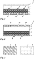
- Fig. 1 shows a first embodiment of a multi-layer body 1. This comprises a support layer 2. On one side of the support layer 2, an optical auxiliary layer 3 is applied, on which in turn a decorative layer 4 is arranged.
- recesses 41 are provided according to the invention, which also penetrate the auxiliary layer 3.
- optically transparent paints or other materials may be arranged in these recesses 41.
- auxiliary layer 3 and the decorative layer 4 side facing away from the carrier layer 2 are contacted by means of which illuminant 6.
- a plastic layer 7 is injection-molded, to which a further optical auxiliary layer 3 'adjoins.
- the carrier layer 2 may be formed as a film. This preferably consists of PET, PEN, PC, PVC, Kapton®, PLA, PMMA or ABS, with a layer thickness of 1 .mu.m to 500 .mu.m, preferably from 20 .mu.m to 300 .mu.m.
- the carrier layer 2 can be designed as a printed circuit board, in particular made of FR4, polyimide or paper, with a layer thickness of 50 ⁇ m to 2 mm, preferably of 100 ⁇ m to 1.5 mm.
- the auxiliary layers 3, 3 ' can be embodied as reflection layers or absorption layers and are intended in particular to ensure that each luminous means 6 is only visible through the associated recess 41, so that scattered light is avoided.
- a reflection layer the luminous efficacy the bulbs are improved at the recesses by laterally scattered light is reflected in the recesses.
- Reflective layers are preferably produced by vapor deposition, sputtering, or the like of a metal, in particular aluminum, silver, chromium, copper, gold, or alloys thereof, with a layer thickness of 1 nm to 500 nm, preferably from 5 nm to 100 nm.
- pigmented paints in particular comprising carbon black pigments, having a layer thickness of from 0.1 ⁇ m to 50 ⁇ m, preferably from 1 ⁇ m to 20 ⁇ m, can be used.
- the decorative layer 4 may also be a printing or lacquer layer.
- this is then applied by printing, in particular by screen printing, gravure printing or pad printing, and / or by painting on the carrier layer and / or the plastic layer.
- the decorative layer 4 can in turn have a plurality of layers or regions with different optical properties, so that complex visual designs can also be created. Specific possibilities for the design of the decorative layer 4 will be explained later with reference to further embodiments.
- the conductor layer 5 is preferably more conductive by vapor deposition, sputtering, electrodeposition or lamination of a metal, in particular aluminum, silver, chromium, copper, gold, or alloys thereof, and / or by applying conductive pigments, nanoparticles, ITO, ATO organic polymers, in particular PEDOT or PANI, carbon nanotubes, graphene or carbon black with a layer thickness of 1 nm to 500 .mu.m, preferably from 10 nm to 50 .mu.m produced.
- the wiring layer 5 can also be integrated into an auxiliary optical layer 3 and thus simultaneously provide optical properties.
- the optical auxiliary layer may be a metallic reflection layer of vapor-deposited, sputtered-on or printed metal layers and, by means of suitable structuring, simultaneously provide correspondingly metallically conductive printed conductors.
- the bulbs 6 are light-emitting diodes.
- SMD LEDs with a length of 400 .mu.m to 20 mm, preferably from 0.6 mm to 2 mm, a width of 200 .mu.m to 5 mm, preferably from 0.3 mm to 1.25 mm, and a height from 200 ⁇ m to 5 mm, preferably from 0.2 mm to 1.5 mm, and / or chip LEDs having a length of from 100 ⁇ m to 2 mm, preferably from 0.2 mm to 0.5 mm, a width of 100 ⁇ m to 2 mm, preferably from 0.2 mm to 0.5 mm, and a height of 50 ⁇ m to 250 ⁇ m, preferably from 75 ⁇ m to 125 ⁇ m.
- OLED organic light emitting diodes
- LEC light emitting cells
- electroluminescent displays can also be used as alternative light sources.
- the plastic layer 7 is preferably produced by injection molding.
- the composite of carrier layer 2 and the layers 3, 4, 5 arranged thereon and the light sources 6 are inserted into a cavity of an injection mold and back-injected with a plastic compound.
- a thermally activated adhesive layer may be applied.
- the plastic compound used is preferably PMMA, ABS, PS, PE, PP, PC, POM, PA, ASA, SAN or TPU. Also combinations of these plastics, either as a mixture or in a multi-component process are possible.
- the injection molding of the plastic layer 7 takes place in a preferably pre-tempered tool at a melt temperature of 150 ° C to 350 ° C, preferably from 200 ° C to 300 ° C and / or a pressure of 500 bar to 2800 bar, preferably from 700 bar to 2500 bar.
- multilayer bodies 1 differ essentially from the number, arrangement and geometric configuration of the layers and components.
- the properties of the individual layers and elements described above are also valid for the following exemplary embodiments.
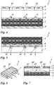
- the decorative layer 4 and the optical auxiliary layer is arranged on a first side of the plastic layer 7 and the carrier layer 2 with the conductor layer 5 and the light emitting means 6 on the opposite side of the plastic layer 7.
- the bulbs point away from the plastic layer 7 and are located in this Case not in overlap with the recesses 41, so that they are backlit indirectly.
- the decorative layer 4 is applied directly to the plastic layer 7 together with the optical auxiliary layer 3 by an IMD process.
- the carrier layer 2 with the LEDs 6 is placed on the decorative layer 4 opposite side of the injection mold with the carrier layer in the direction of the injection molding compound.
- the decoration and application of the carrier layer 2 on the plastic layer 7 can be done in one operation.
- the embodiment according to Fig. 4 built up. It differs from the embodiment Fig. 2 merely in that the carrier layer 2 is aligned with the light sources 6 and the conductor layer 5 to the plastic layer 7 out and that the bulbs 6 are in register with the recesses 41, so that they are backlit directly.
- a further auxiliary layer 3 ' is arranged, which prevents the light emission on this page and / or reflected to the rear reflected light forward to improve the light output.
- this optical auxiliary layer 3 ' made absorbent.
- Fig. 5 is the plastic layer 7 as in the embodiment according to Fig. 1 molded on one side.
- decor layer 4 conductor layer 5 and light elements 6 are arranged on the same side of the carrier layer 2 and aligned to the plastic layer 7 out.
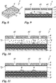
- Fig. 6 shows a plan view of a further embodiment of a multi-layer body 1.
- the same multi-layer body 1 is in Fig. 7 shown in a schematic sectional view.
- the light of the LEDs 6 is decoupled here indirectly. These are preferably not positioned below a recess 41 in the decorative layer 4. This can be particularly advantageous if the light is to be distributed homogeneously over larger or distributed smaller outlet openings 41.
- the optional optical auxiliary layers 3, 3 ' are designed to be reflective, for example as a mirror-deposited or sputtered metal layer, so that as much light as possible is reflected into the outlet openings 41.
- the Decor layers 4 change the color of the LED light when switched on. This can be achieved by the decorative layer 4wie in Fig. 6 shown continuously over the LEDs 6 is executed. In this case, the decorative layer areas 42, 43 having different colors, structures and transparencies, which form the desired decor.
- the luminous structures are preferably produced via a metallic or particularly light-tight layer 3 which contains the structure to be displayed as recesses (ie forms a shadow mask below the decor layer 4).
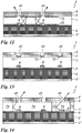
- the in Fig. 1 layer sequence shown are used, with the difference that the decorative layer 4 is printed without recesses 41.
- the decorative layer 4 can contain recesses 41 directly above the LEDs 6 in the viewing direction, as in FIGS FIGS. 8 and 9 shown.
- the optical auxiliary layers 3, 3 'lying outside the direct beam path of the LEDs 6 should be designed to be as light-absorbent as possible in order to prevent light from escaping in adjacent recesses 41 (crosstalk or optical "crosstalk").
- a homogenization of the light can be achieved by the use of many LEDs 6 (very expensive and expensive) or by the use of scattering particles 71, and / or homogeneously distributed fluorescent dyes in the injection molding compound of the plastic layer 7 and / or the carrier layer 2. This is in Fig. 10 shown.
- color effects can be generated by the coloring of the material and / or fluorescence.
- soluble Fluorescent dyes can also be used insoluble fluorescent pigments, which then serve as light-scattering particles 71 at the same time.
- the light-scattering particles 71 may include inorganic pigments and / or particles, in particular of silicon dioxide, fumed silica, titanium dioxide, zinc sulfide or a metal having a particle size of 5 nm to 500 ⁇ m, preferably of 500 nm to 100 ⁇ m.
- fine optical grating 72 may be incorporated, which prevent or support the decoupling of the light.
- Preferred grating parameters are for subwavelength grating a period preferably from 200 nm to 500 nm and a grating depth preferably from 100 nm to 500 nm.
- the grating type is here preferably selected from the series linear, cross or hexagonal lattice.
- the lateral extent dx or dy of the prisms is 1 ⁇ m to 100 ⁇ m, preferably 5 ⁇ m to 50 ⁇ m.
- the texture depth is preferably about 0.3 to 2 times the lateral extent.
- the arrangement of the microprisms can be both regular, that is periodic as well as random and pseudo-random.
- the optical grating 72 over the entire surface (see Fig. 11 ) or only in the region of the recesses 41 (see Fig. 13 ) may be arranged in the decorative layer 4 and / or the optical auxiliary layer 3 and / or the plastic layer 7.
- the production occurs e.g. by replication or by structuring of the injection molding tool, so that the grids 72 are molded during the injection molding of the plastic layer 7.
- a further optical grating 21 can be embodied on the carrier layer 2, as in FIG Fig. 12 shown.
- the Recesses 41 are not covered by the grid 72.
- the arrows indicate a possible beam path of the light emitted by the LEDs 6.
- the use of two different injection molding compounds with different optical refractive index, which respectively form subregions 73, 74 of the plastic layer 7, can be used to produce lens effects, in particular by refraction of light, as in US Pat Fig. 15 shown, or to reflect the light at interfaces, as in Fig. 14 shown.
- Crosstalk ie, an optical "crosstalk" between a plurality of outlet openings 41 can be prevented or the light output at the outlet openings 41 can be improved.
- the plastic layer 7 is formed in these cases by two-component injection molding. Either regions 73, 74 are injected in separate dies, i. First, the area 73 is sprayed on the LEDs 6, removed the workpiece and placed in a second tool. There, the area 74 is then injected.
- a turntable At first, e.g. the area 73 sprayed. Then the tool is opened and the component rotates with the turntable by half a turn further, so that it faces a second tool insert. There, the area 74 is then injected.
- the area 73 is attached to a second workpiece. After spraying area 74 on the first workpiece, the finished first workpiece is removed and the turntable rotates again by half a turn.
- the following embodiments relate to the electrical contacting of the conductor layer 5. This can be realized by direct galvanic contact but also contactless.
- a through-connection 8 (VIA, vertical interconnect access) can be attached through the carrier layer 2, as in FIG Fig. 16 shown.
- VIP vertical interconnect access
- a plated-through hole 8 can be produced, for example galvanically, by a targeted deposition of metal within a previously created hole within the carrier layer 2 or by punching a metal pin. Also conceivable is the use of a KrimpTechnik. Both happen before the carrier layer 2 is processed by injection molding.
- Another possibility for contacting by means of crimping is the use of a second interconnect substrate 9, which, as in FIG Fig. 17 shown, placed on the side of the wiring layer 5 on the support layer 2 and anchored by Krimptechnik.
- This mechanically produced connection can either be produced in a separate step before the injection molding process or during this, with the aid of an integrated crimping tool.
- this step may be performed separately before the back injection process.
- An indirect contacting of the conductor layer 5 can be capacitive, as in Fig. 18 shown.
- the basis of capacitive coupling is two Coupling surfaces 51 within the conductor layer 5 which must be positioned in each case at least partially over associated outside located coupling surfaces 10.
- an opposing field builds up on the capacitors formed by the respectively superimposed coupling surfaces 10, 51, so that a current can flow through the loads contacted by the conductor layer 5.
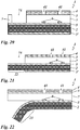
- antenna structures 52, 11 arranged in analogy thereto can also be used so as to realize an inductive coupling. Ideally, these are tuned so that the external transmit antenna 11 operates in resonance with the internal receive antenna 52.
- the basic construction is Fig. 19 shown.
- an alternating current is generated in the interconnect layer 5 via the inductive coupling, without having to be contacted directly.
- a rectification can also be done by means of suitable components.
- the resonance frequency and range can be adjusted.
- information or control commands can also be transmitted to the embedded electronics integrated on the carrier layer.
- the external antenna 52 can also be applied directly to the carrier layer 2 or attached after completion of the multi-layer body 1.
- Another possibility for direct contacting of the conductor layer 5 is that they do not completely enclose with plastic during the injection molding of the plastic layer 7.
- a recess 75 can be left open in the plastic layer 7, as in Fig. 20 shown, or the plastic layer 7 are not applied to the edge of the carrier layer 2, so that there is a protruding tab 22 of the carrier layer on which the conductor layer 5 can be contacted (see Fig. 21 ).
- a portion 23 of the carrier layer 2, on which the conductor track layer 5 extends are detached from the plastic layer 7.
- a corresponding release layer can be applied to the subregion 23 prior to injection molding.
- the release layer preferably consists of a wax, a siloxane polymer or a fluorine-containing polymer (eg Teflon®) and has a layer thickness of 10 nm to 5 ⁇ m, preferably of 100 nm to 1 ⁇ m.
Landscapes
- Engineering & Computer Science (AREA)
- Microelectronics & Electronic Packaging (AREA)
- Manufacturing & Machinery (AREA)
- Power Engineering (AREA)
- Mechanical Engineering (AREA)
- Computer Hardware Design (AREA)
- General Physics & Mathematics (AREA)
- Condensed Matter Physics & Semiconductors (AREA)
- Physics & Mathematics (AREA)
- Injection Moulding Of Plastics Or The Like (AREA)
- Optical Elements Other Than Lenses (AREA)
- Optical Filters (AREA)
- Diffracting Gratings Or Hologram Optical Elements (AREA)
- Non-Portable Lighting Devices Or Systems Thereof (AREA)
- Illuminated Signs And Luminous Advertising (AREA)
- Laminated Bodies (AREA)
Description
Die Erfindung betrifft ein Verfahren zum Herstellen eines Mehrschichtkörpers sowie einen derart hergestellten Mehrschichtkörper.The invention relates to a method for producing a multilayer body and to a multilayer body produced in this way.
Bei der Herstellung von Kunststoffbauteilen ist in zunehmendem Maße neben einer Dekoration auch die Integration elektronischer Funktionen gefordert. So werden schon seit langem Kunststoffteile mit Beleuchtungselementen versehen, um den Nutzer auf einen bestimmten Gerätezustand hinzuweisen (z.B. Schaltelemente in einem Kraftwagen, Bedienblenden von Haushaltsgeräten).In the manufacture of plastic components is increasingly required in addition to a decoration and the integration of electronic functions. For example, plastic parts have long been provided with lighting elements to alert the user to a particular device condition (e.g., automotive trim elements, home appliance control panels).
Üblicherweise muss dazu das bereits dekorierte Kunststoffteil in einem zusätzlichen Fertigungsschritt mit einer konventionellen Platine verbunden werden, die Leuchtelemente, beispielsweise Leuchtdioden, und/oder andere elektronische Bauteile trägt. Oftmals müssen in weiteren Fertigungsschritten zusätzliche Schichten zwischen Kunststoffblende und dem Leuchtelement eingebaut werden, die zum Beispiel eine Punktlichtquelle wie eine Leuchtdiode in einen Flächenstrahler verwandeln (Diffusorfolien in Form einer zusätzlichen Schicht) oder das Licht zu verschiedenen Positionen leiten (Lichtleiter in Form einer zusätzlichen Schicht). Die LED-Platine muss zudem mittels Steckverbindungen an eine Hauptplatine oder einen Controller des Gerätes angeschlossen werden.Usually, the already decorated plastic part must be connected in an additional manufacturing step with a conventional board that carries lighting elements, such as light emitting diodes, and / or other electronic components. Often, additional layers between the plastic diaphragm and the light-emitting element must be installed in further manufacturing steps, which, for example, transform a point light source such as a light-emitting diode into a surface radiator (diffuser foils in the form of an additional light source Layer) or direct the light to different positions (optical fiber in the form of an additional layer). The LED board must also be connected by plug connections to a motherboard or a controller of the device.
Die
Die
Das Dokument XP055204300 offenbart eine selbstleuchtende Seitenbegrenzung für LKW.The document XP055204300 discloses a self-luminous lateral boundary for trucks.
Die
Insgesamt ist daher die Herstellung solcher dekorierter Kunststoffbauteile mit integrierten elektronischen Funktionen aufwändig und teuer.Overall, therefore, the production of such decorated plastic components with integrated electronic functions is complex and expensive.
Aufgabe der vorliegenden Erfindung ist es somit, ein besonders einfaches und kostengünstiges Verfahren zum Herstellen eines Mehrschichtkörpers mit integriertem Dekor und elektronischen Funktionen, sowie einen solchen Mehrschichtkörper anzugeben.The object of the present invention is therefore to provide a particularly simple and cost-effective method for producing a multilayer body with integrated decor and electronic functions, as well as such a multilayer body.
Erfindungsgemäß wird diese Aufgabe mit dem Gegenstand der Ansprüche 1 und 12 gelöst.According to the invention this object is achieved with the subject matter of
Unter einer "Lage" soll dabei ein vorzugsweise im Wesentlichen flächiges Gebilde verstanden werden, welches selbst wiederum aus mehreren Schichten bestehen kann. Es kann sich dabei beispielsweise um eine Folie oder eine Platine handeln. Alternativ sind jedoch auch komplexere dreidimensionale Geometrien möglich, insbesondere für die im Spritzguss hergestellte Kunststofflage.A "layer" is to be understood as a preferably substantially flat structure, which in turn may itself consist of several layers. It may be, for example, a film or a board. Alternatively, however, more complex three-dimensional geometries are possible, especially for the plastic layer produced by injection molding.
Eine solche Lage muss dabei nicht notwendigerweise ein eigenständiges Bauteil darstellen, beispielsweise kann eine Dekorlage auch durch Drucken auf einen Untergrund gebildet werden.Such a layer need not necessarily represent an independent component, for example, a decorative layer can also be formed by printing on a substrate.
Die Verbindung von Dekorlage, Trägerlage und Kunststofflage kann somit in einem einzigen Arbeitsschritt erfolgen. Eine nachträgliche Montage elektronischer Bauelemente ist nicht notwendig, so dass die Herstellung eines Mehrschichtkörpers mit integriertem Dekor und integrierter Beleuchtung auf diese Weise besonders einfach und kostengünstig ist. Ferner wird so ein besonders stabiler und haltbarer Mehrschichtkörper geschaffen, dessen Schichten prozesssicher in einer definierten Lagebeziehung angeordnet werden können.The connection of decorative layer, carrier layer and plastic layer can thus be done in a single step. A subsequent assembly of electronic components is not necessary, so that the production of a multi-layer body with integrated decor and integrated lighting in this way is particularly simple and inexpensive. Furthermore, a particularly stable and durable multi-layer body is created, the layers of which can be arranged reliably in a defined positional relationship.
Bezüglich der relativen Anordnung der Lagen bestehen mehrere Möglichkeiten:
Zunächst ist es möglich, dass die Dekorlage auf die Trägerlage aufgebracht wird. Dies kann vor dem Spritzgießen der Kunststofflage erfolgen, so dass Dekorlage und Trägerlage gemeinsam hinter- oder umspritzt werden. Es ist jedoch auch möglich, die Dekorlage erst nach dem Spritzgießen anzubringen, beispielsweise durch Laminieren einer Folie oder durch Drucken auf den Verbund aus Träger- und Kunststofflage. Träger- und Dekorlage können auch gemeinsam in das Spritzgusswerkzeug eingelegt werden, so dass sie in direktem Kontakt stehen und während des Spritzgießens verbunden werden. Dazu kann eine der Lagen beispielsweise mit einem wärmeaktivierbaren Klebstoff versehen werden, der unter den Druck- und Temperaturbedingungen des Spritzgussvorgangs aktiviert wird.Regarding the relative arrangement of the layers there are several possibilities:
First, it is possible that the decorative layer is applied to the carrier layer. This can be done before the injection molding of the plastic layer, so that the decorative layer and carrier layer are back-injected together or. However, it is also possible to apply the decorative layer only after the injection molding, for example by laminating a film or by printing on the composite of carrier and plastic layer. Carrier and decorative layer can also be placed together in the injection mold, so that they are in direct contact and connected during injection molding. For this purpose, one of the layers, for example, with a heat-activated Adhesive, which is activated under the pressure and temperature conditions of the injection molding process.
Es ist dabei möglich, dass die Dekorlage auf die dem zumindest einen Leuchtmittel abgewandte Seite der Trägerlage aufgebracht wird. Das Licht des zumindest einen Leuchtmittels tritt dann sowohl durch die Trägerlage als auch durch die Dekorlage. Die Trägerlage selbst kann damit ebenfalls als farbgebende Schicht, als Diffusor oder als ähnliches optisches Element dienen.It is possible that the decorative layer is applied to the side facing away from the at least one light source side of the carrier layer. The light of the at least one light source then passes both through the carrier layer and through the decorative layer. The carrier layer itself can thus also serve as a coloring layer, as a diffuser or as a similar optical element.
Alternativ kann die Dekorlage auch auf die dem zumindest einen Leuchtmittel zugewandte Seite der Trägerlage, insbesondere zwischen dem Leuchtmittel und der Trägerlage, aufgebracht werden. Hierdurch wird ein kürzerer Strahlengang für das austretende Licht verwirklicht, so dass geringere Absorptionsverluste auftreten.Alternatively, the decorative layer can also be applied to the side of the carrier layer facing the at least one luminous means, in particular between the luminous means and the carrier layer. As a result, a shorter beam path for the exiting light is realized, so that lower absorption losses occur.
Hierbei kann die Trägerlage auch ablösbar gestaltet werden, so dass sie nach dem Hinterspritzen entfernt werden kann. Es verbleiben dann lediglich die Leuchtmittel und die Dekorlage, sowie gegebenenfalls weitere funktionale Elemente wie Leiterbahnen oder dergleichen an der Kunststofflage.In this case, the carrier layer can also be made detachable, so that it can be removed after the back molding. Only the lighting means and the decorative layer, as well as possibly further functional elements such as strip conductors or the like on the plastic layer then remain.
Es ist dabei zweckmäßig, wenn die Dekorlage und die Trägerlage in einer Formhälfte des Spritzgusswerkzeugs fixiert werden, insbesondere durch mechanische Klemmmittel und/oder Vakuum, und einseitig hinterspritzt werden.Das Hinterspritzen kann dabei auf Seite der Dekorlage oder auch der Trägerlage erfolgen. Dabei ist es vorteilhaft, wenn die nicht zu hinterspritzende Lage flächig an einer Wandung des Spritzgusswerkzeugs anliegt, so dass diese Lage zuverlässig nicht in Kontakt mit der Kunststoffmasse kommt.It is expedient if the decorative layer and the carrier layer are fixed in a mold half of the injection mold, in particular by mechanical clamping means and / or vacuum, and injected behind on one side. The injection molding can be done on the side of the decorative layer or the carrier layer. It is advantageous if the non-back-injected layer is applied flat against a wall of the injection molding tool, so that this position reliably does not come into contact with the plastic mass.
Es ist ferner möglich, dass die Kunststofflage zwischen der dem zumindest einen Leuchtmittel abgewandten Seite der Trägerlage und der Dekorlage angespritzt wird.It is also possible for the plastic layer to be injection-molded between the side of the carrier layer facing away from the at least one luminous means and the decorative layer.
Alternativ kann die Kunststofflage auch zwischen der dem zumindest einen Leuchtmittel zugewandten Seite der Trägerlage und der Dekorlage angespritzt werden.Alternatively, the plastic layer can also be injection-molded between the side of the carrier layer facing the at least one luminous means and the decorative layer.
Dabei werden Träger- und Dekorlage beispielsweise in die jeweils gegenüberliegenden Hälften eines Spritzgusswerkzeugs eingelegt, ohne dass sie in direktem Kontakt stehen und die Kunststofflage in den Zwischenraum zwischen Träger- und Dekorlage eingespritzt. Dazu können sowohl die Trägerals auch die Dekorlage mit einem wärmeaktivierbaren Klebstoff versehen werden, der unter den Druck- und Temperaturbedingungen des Spritzgussvorgangs aktiviert wird.Carrier and decorative layer are inserted, for example, in the respective opposite halves of an injection mold, without being in direct contact and the plastic layer injected into the space between the carrier and decorative layer. For this purpose, both the carrier and the decorative layer can be provided with a heat-activatable adhesive, which is activated under the pressure and temperature conditions of the injection molding process.
In diesen beiden Varianten resultiert also ein Sandwichaufbau, bei dem die Kunststofflage von der Trägerlage und der Dekorlage eingeschlossen ist. Dabei können die Leuchtmittel von außen zugänglich bleiben oder vollständig im Kunststoff eingekapselt werden.In these two variants thus results in a sandwich construction in which the plastic layer is enclosed by the carrier layer and the decorative layer. The bulbs can remain accessible from the outside or be completely encapsulated in the plastic.
Dabei ist es zweckmäßig, wenn die Dekorlage in einer ersten Formhälfte des Spritzgusswerkzeugs und die Trägerlage in einer zweiten Formhälfte des Spritzgusswerkzeugs fixiert wird, insbesondere durch mechanische Klemmmittel und/oder durch Vakuum.It is expedient if the decorative layer is fixed in a first mold half of the injection mold and the carrier layer in a second mold half of the injection mold, in particular by mechanical clamping means and / or by vacuum.
Bevorzugt liegen die jeweiligen Lagen dabei wiederum flächig an einer Innenwandung des Formwerkzeugs an, so dass sie nur einseitig mit der Kunststoffmasse in Kontakt kommen.In this case, the respective layers are in turn applied flatly to an inner wall of the molding tool, so that they only come into contact with the plastic compound on one side.
Zweckmäßigerweise weist die Dekorlage eine Schichtdicke von 0,1 µm bis 50 µm auf, bevorzugt von 1 µm bis 20 µm.Conveniently, the decorative layer has a layer thickness of 0.1 .mu.m to 50 .mu.m, preferably from 1 .mu.m to 20 .mu.m.
Die Dekorlage kann dabei als eigenständiges Element bereitgestellt werden, beispielsweise in Form einer Folie, die selbst wiederum mehrere Schichten, beispielsweise Druck- oder Lackschichten, aufweisen kann.The decorative layer can be provided as an independent element, for example in the form of a film, which in turn can have several layers, for example printing or lacquer layers.
Alternativ kann die Dekorlage durch Drucken, insbesondere durch Aufgießen, Siebdruck, Tiefdruck oder Tampondruck, und/oder durch Lackieren auf der Trägerlage und/oder der Kunststofflage bereitgestellt werden.Alternatively, the decorative layer can be provided by printing, in particular by pouring, screen printing, gravure or pad printing, and / or by coating on the carrier layer and / or the plastic layer.
Die Trägerlage wird bevorzugt als Folie, insbesondere aus PET (Polyethylen), PEN (Polyethylennaphthalat), PC (Polycarbonat), PVC (Polyvinylchlorid), Kapton® (Poly-oxydiphenylen-pyromellitimid) oder anderen Polyimiden, PLA (Polylactat), PMMA (Polymethylmethacrylat) oder ABS (Acrylnitrilbutadienstyrol), mit einer Schichtdicke von 1 µm bis 500 µm, bevorzugt von 20 µm bis 300 µm bereitgestellt.The carrier layer is preferably used as a film, in particular made of PET (polyethylene), PEN (polyethylene naphthalate), PC (polycarbonate), PVC (polyvinyl chloride), Kapton® (polyoxydiphenylenepyromellitimide) or other polyimides, PLA (polylactate), PMMA (polymethyl methacrylate ) or ABS (acrylonitrile butadiene styrene), with a layer thickness of 1 .mu.m to 500 .mu.m, preferably from 20 .mu.m to 300 .mu.m.
Mit solchen Trägerfolien können besonders dünne und gegebenenfalls auch flexible Mehrschichtkörper hergestellt werden.With such carrier films, it is possible to produce particularly thin and possibly also flexible multilayer bodies.
Alternativ kann die Trägerlage als Leiterplatte, insbesondere aus FR4 (Glasfasergewebe in Epoxidharzmatrix), Polyimid oder Papier, mit einer Schichtdicke von 50 µm bis 2 mm, bevorzugt von 100 µm bis 1,5 mm bereitgestellt werden.Alternatively, the carrier layer can be provided as a printed circuit board, in particular made of FR4 (glass fiber fabric in epoxy resin matrix), polyimide or paper, with a layer thickness of 50 μm to 2 mm, preferably 100 μm to 1.5 mm.
Hierdurch können insbesondere Mehrschichtkörper mit besonders guter mechanischer Stabilität hergestellt werden, die sich auch zum Einsatz unter anspruchsvollen Bedingungen eignen.As a result, in particular multilayer bodies with particularly good mechanical stability can be produced, which are also suitable for use under demanding conditions.
Bevorzugt wird zum Spritzgießen der Kunststofflage zumindest eine Kunststoffmasse aus PMMA (Polymethylmethacrylat), ABS (Acrylnitrilbutadienstyrol), PS (Polystyrol), PE (Polyethylen), PP (Polypropylen), PC (Polycarbonat), POM (Polyoxymethylen), PA (Polyamid), ASA(Acrylnitrilstyrolacrylat), SAN (Styrol-Acrylnitril) oder TPU (thermoplastisches Polyurethan) verwendet.For injection molding of the plastic layer, preference is given to at least one plastic compound of PMMA (polymethyl methacrylate), ABS (acrylonitrile butadiene styrene), PS (polystyrene), PE (polyethylene), PP (polypropylene), PC (polycarbonate), POM (polyoxymethylene), PA (polyamide), ASA (acrylonitrile styrene acrylate), SAN (styrene-acrylonitrile) or TPU (thermoplastic polyurethane) used.
Durch die Wahl des geeigneten Kunststoffmaterials können die Materialeigenschaften des Mehrschichtkörpers je nach dessen gewünschtem Einsatzgebiet über einen weiten Bereich variiert werden.By choosing the appropriate plastic material, the material properties of the multilayer body can be varied over a wide range depending on the desired field of use.
Es ist dabei auch möglich, mehrere Kunststoffe zu kombinieren, entweder als Gemisch oder im Rahmen eines Mehrkomponenten-Spritzgussverfahrens.It is also possible to combine several plastics, either as a mixture or as part of a multi-component injection molding process.
Vorzugsweise wird das Spritzgießen der Kunststofflage in einem vortemperierten Werkzeug bei einer Massetemperatur von 150°C bis 350°C, bevorzugt von 200°C bis 300°C und/oder einem Druck von 500 bar bis 2800 bar, bevorzugt von 700 bar bis 2500 bar durchgeführt.Preferably, the injection molding of the plastic layer in a pre-tempered tool at a melt temperature of 150 ° C to 350 ° C, preferably from 200 ° C to 300 ° C and / or a pressure of 500 bar to 2800 bar, preferably from 700 bar to 2500 bar carried out.
Es ist vorteilhaft, wenn zum Spritzgießen der Kunststofflage ein Spritzgusswerkzeug verwendet wird, welches eine Kavität mit zumindest zwei bereichsweise ebenen und parallelen Innenwandungen aufweist.
Werden die Trägerlage und die Dekorlage vor dem Spritzgießen der Kunststofflage an eine bzw. beide dieser Innenwandungen angelegt, so kann ein flächiger Mehrschichtkörper erhalten werden.It is advantageous if an injection molding tool is used for injection molding of the plastic layer, which has a cavity with at least two partially planar and parallel inner walls.
If the carrier layer and the decorative layer are applied to one or both of these inner walls prior to the injection molding of the plastic layer, then a laminar multi-layer body can be obtained.
Alternativ kann zum Spritzgießen der Kunststofflage auch ein Spritzgusswerkzeug verwendet werden, welches eine Kavität mit zumindest einer bereichsweise gekrümmten Innenwandung aufweist.Alternatively, an injection molding tool can be used for injection molding of the plastic layer, which has a cavity with at least one partially curved inner wall.
Auf diese Weise können auch Mehrschichtkörper mit komplexeren dreidimensionalen Geometrien erhalten werden. Die Krümmung kann dabei auch nur bereichsweise vorliegen. Es ist dabei ferner möglich, durch den Einsatz von Schiebern und/oder Kernen innerhalb der Kavität die Geometrie des Mehrschichtkörpers weiter zu beeinflussen. Insgesamt stehen hier alle üblichen, aus dem Spritzguss bekannten Gestaltungsmöglichkeiten zur Verfügung.In this way, multi-layer bodies with more complex three-dimensional geometries can be obtained. The curvature can also be present only partially. It is also possible to further influence the geometry of the multilayer body through the use of sliders and / or cores within the cavity. Overall, all the usual design options known from injection molding are available here.
Es ist ferner zweckmäßig, wenn als Leuchtmittel SMD-LEDs (SMD = Surface Mounted Device)mit einer Länge von 400 µm bis 20 mm, bevorzugt von 0,6 mm bis 2 mm, einer Breite von 200 µm bis 5 mm, bevorzugt von 0,3 mm bis 1,25 mm, und einer Höhe von 200 µm bis 5 mm, bevorzugt von 0,2 mm bis 1,5 mm, und/oder Chip-LEDs mit einer Länge von 100 µm bis 2 mm, bevorzugt von 0,2 mm bis 0,5 mm, einer Breite von 100 µm bis 2 mm, bevorzugt von 0,2 mm bis 0,5 mm, und einer Höhe von 50 µm bis 250 µm, bevorzugt von 75 µm bis 125 µm, verwendet werden.It is also expedient for SMD LEDs (SMD = Surface Mounted Device) with a length of 400 μm to 20 mm, preferably of 0.6 mm to 2 mm, a width of 200 μm to 5 mm, preferably of 0, to be used as the light source , 3 mm to 1.25 mm, and a height of 200 microns to 5 mm, preferably from 0.2 mm to 1.5 mm, and / or chip LEDs having a length of 100 microns to 2 mm, preferably from 0 , 2 mm to 0.5 mm, a width of 100 microns to 2 mm, preferably from 0.2 mm to 0.5 mm, and a height of 50 microns to 250 microns, preferably from 75 microns to 125 microns, are used ,
Als alternative Leuchtmittel können grundsätzlich auch organische Leuchtdioden (OLED), Light Emitting Cells (LEC) oder Elektrolumineszenz-Displays verwendet werden.In principle, organic light emitting diodes (OLED), light emitting cells (LEC) or electroluminescent displays can also be used as alternative light sources.
Des Weiteren können neben den Leuchtelementen noch zusätzliche Bauteile, wie z.B. Logikschaltungen, Widerstände, Dioden, Piezolautsprecher, die mit den Leuchtelementen verschaltet werden integriert werden. Die Leuchtelemente werden unter Anderen zur Anzeige von Informationszuständen eingesetzt, alternativ oder zusätzlich lassen sich auch reflektive, nicht selbst leuchtende Anzeigeelemente auf den Träger integrieren, wie z.B. elektrophoretische oder elektrochrome Displays.Furthermore, in addition to the lighting elements, additional components, such as e.g. Logic circuits, resistors, diodes, piezo loudspeakers that are interconnected with the lighting elements are integrated. The light-emitting elements are used inter alia for the display of information states, alternatively or additionally, reflective, not self-luminous display elements can be integrated on the support, such. electrophoretic or electrochromic displays.
Es wird zumindest eine optische Hilfsschicht, insbesondere eine Reflektionsschicht oder Absorptionsschicht, auf die Dekorlage und/oder die Trägerlage und/oder die angespritzte Kunststofflage aufgebracht.At least one optical auxiliary layer, in particular a reflection layer or absorption layer, is applied to the decorative layer and / or the carrier layer and / or the molded-on plastic layer.
Durch solche Hilfsschichten kann die Lichtführung innerhalb des Mehrschichtkörpers kontrolliert werden. Es ist dabei beispielsweise möglich, einen nur einseitigen Lichtaustritt sicherzustellen oder störendes Streulicht zu vermeiden. Derartige Hilfsschichten können auch lediglich partiell aufgebracht werden und so beispielsweise definierte Austrittsöffnung für das Licht des wenigstens einen Leuchtmittels bereitstellen.By such auxiliary layers, the light guide can be controlled within the multilayer body. It is possible, for example, to ensure only one-sided light emission or to avoid disturbing scattered light. Such auxiliary layers can also be applied only partially and thus provide, for example, defined outlet opening for the light of the at least one luminous means.
Für die Herstellung von Reflektionsschichten ist es vorteilhaft, wenn die zumindest eine optische Hilfsschicht durch Aufdampfen oder Sputterneines Metalls, insbesondere Aluminium, Silber, Chrom, Kupfer, Gold, oder Legierungen davon mit einer Schichtdicke von 1 nm bis 500 nm, bevorzugt von 5 nm bis 100 nm, erzeugt wird.For the production of reflection layers, it is advantageous if the at least one auxiliary optical layer by vapor deposition or sputtering of a metal, in particular aluminum, silver, chromium, copper, gold, or alloys thereof with a layer thickness of 1 nm to 500 nm, preferably from 5 nm 100 nm, is generated.
Alternativ kann die Reflexionsschicht auch durch Drucken von Metallpigment-haltigen Lacken mit einer Schichtdicke von 0,1 µm bis 50 µm, bevorzugt von 1 µm bis 20 µm, erzeugt werden.Alternatively, the reflective layer can also be produced by printing lacquers containing metal pigments having a layer thickness of from 0.1 μm to 50 μm, preferably from 1 μm to 20 μm.
Um Absorptionsschichten aufzubringen, ist es zweckmäßig, wenn die zumindest eine optische Hilfsschicht durch Aufbringen eines pigmentierten Lacks, insbesondere umfassend Rußpigmente, mit einer Schichtdicke von 0,1 µm bis 50 µm, bevorzugt von 1 µm bis 20 µm, erzeugt wird.In order to apply absorption layers, it is expedient if the at least one auxiliary optical layer is produced by applying a pigmented lacquer, in particular comprising carbon black pigments, with a layer thickness of 0.1 μm to 50 μm, preferably of 1 μm to 20 μm.
Es ist ferner vorteilhaft, wenn die bereitgestellte Dekorlage zumindest einen ersten Bereich, welcher bezüglich des Spektrums des von dem zumindest einen Leuchtmittel emittierten Lichts zumindest teiltransparent ist, und zumindest einen zweiten Bereich, welcher bezüglich des Spektrums des von dem zumindest einen Leuchtmittel emittierten Lichts intransparent, d.h. undurchsichtig bzw. opak ist, umfasst.It is further advantageous if the provided decorative layer is at least a first region which is at least partially transparent with respect to the spectrum of the light emitted by the at least one luminous means, and at least one second region which is non-transparent with respect to the spectrum of the light emitted by the at least one luminous means. ie is opaque.
Auch so kann der Lichtaustritt aus dem Mehrschichtkörper kontrolliert werden. Die ersten und zweiten Bereiche können dabei einfache Anzeigeflächen oder auch komplexe optische Informationen bilden.Even so, the light emission from the multi-layer body can be controlled. The first and second areas can form simple display areas or even complex optical information.
Es ist weiter bevorzugt, wenn die Dekorlage so angeordnet wird, dass das zumindest eine Leuchtmittel senkrecht zur Oberfläche der Dekorlage gesehen in Überdeckung mit dem zumindest einen ersten Bereich kommt.It is further preferred if the decorative layer is arranged so that the at least one lamp perpendicular to the surface of the decorative layer seen in overlapping with the at least one first area.
Auf diese Weise kann ein direkter Lichtaustritt verwirklicht werden. Dies kann beispielsweise zur Punktbeleuchtung von Anzeigeflächen verwendet werden.In this way, a direct light emission can be realized. This can be used, for example, for spot lighting of display surfaces.
Alternativ kann die Dekorlage so angeordnet werden, dass das zumindest ein Leuchtmittel senkrecht zur Oberfläche der Dekorlage gesehen in Überdeckung mit dem zumindest einen zweiten Bereich kommt.Alternatively, the decorative layer can be arranged so that the at least one lamp perpendicular to the surface of the decorative layer seen in overlap with the at least one second area.
Damit ist kein direkter Lichtaustritt durch den ersten Bereich möglich. Dies kann beispielsweise zur gleichmäßigen Hinterleuchtung von flächigen Strukturen benutzt werden.Thus, no direct light emission through the first area is possible. This can be used for example for the uniform backlighting of flat structures.
Direkte und indirekte Auskoppelung des von dem wenigstens einen Leuchtmittel erzeugten Lichts können selbstverständlich auch kombiniert werden, um ansprechende optische Effekte zu verwirklichen.Of course, direct and indirect decoupling of the light generated by the at least one luminous means can also be combined in order to realize attractive optical effects.
Es ist weiter vorteilhaft, wenn dem zum Spritzgießen der Kunststofflage verwendeten Kunststoffmaterial und/oder einem eine Schicht der Trägerlage bildenden Material Farbmittel, insbesondere Farbstoffe und/oder Pigmente und/oder Partikel und/oder Quantenpunktmaterialien und oder phosphoreszierende Materialien, zugesetzt werden, welche im Wellenlängenbereich des von dem zumindest einen Leuchtmittel emittierten Lichts absorbieren und/oder streuen und/oder zur Fluoreszenz oder Phosphoreszenz im sichtbaren Wellenlängenbereich anregbar sind.It is also advantageous if colorants, in particular dyes and / or pigments and / or particles and / or quantum dot materials and / or phosphorescent materials, which are in the wavelength range, are added to the plastic material used for injection molding of the plastic layer and / or to a layer of the carrier layer absorb and / or scatter the light emitted by the at least one light source and / or are excitable for fluorescence or phosphorescence in the visible wavelength range.
Hierdurch kann eine Homogenisierung der Lichtverteilung in der Kunststofflage und/oder Trägerlage erreicht werden. Dies eignet sich insbesondere, um gleichmäßig hinterleuchtete Flächen zu schaffen.In this way, a homogenization of the light distribution in the plastic layer and / or carrier layer can be achieved. This is particularly suitable for creating evenly backlit surfaces.
Gleichzeitig oder alternativ kann hiermit, insbesondere bei der Verwendung von fluoreszierenden oder absorbierenden Substanzen oder Quantenpunkten, das Spektrum des von dem wenigstens einen Leuchtmittel emittierten Lichts gezielt beeinflusst werden, so dass vielfältige Farbeffekte geschaffen werden können.At the same time or alternatively, the spectrum of the light emitted by the at least one luminous means can hereby be specifically influenced, in particular when using fluorescent or absorbing substances or quantum dots, so that a variety of color effects can be created.
Es ist dabei zweckmäßig, wenn die zugesetzten Farbmittel anorganische Pigmente und/oder Partikel, insbesondere aus Siliziumdioxid, pyrogener Kieselsäure, Titandioxid, Zinksulfid oder einem Metall, mit einer Partikelgröße von 5 nm bis 500 µm, bevorzugt von 500 nm bis 100 µm, umfassen.It is expedient for the added colorants to comprise inorganic pigments and / or particles, in particular of silicon dioxide, fumed silica, titanium dioxide, zinc sulfide or a metal, with a particle size of 5 nm to 500 μm, preferably of 500 nm to 100 μm.
Ferner ist es vorteilhaft, wenn eine Oberfläche der Trägerlage mattiert wird.Furthermore, it is advantageous if a surface of the carrier layer is matted.
Auch hierdurch kann die Leuchtdichte über die Trägerlage hinweg homogenisiert werden, um gleichmäßige Leuchtflächen zu erhalten. Auf zusätzliche Diffusoren kann so verzichtet werden.This also makes it possible to homogenize the luminance over the carrier layer in order to obtain uniform luminous surfaces. On additional diffusers can be dispensed with.
Es ist weiter vorteilhaft, wenn eine Dekorlage bereitgestellt wird, welche eine Mehrzahl von Bereichen aufweist, die sich in Farbe und/oder Transparenz bezüglich des Spektrums des von dem zumindest einen Leuchtmittel emittierten Licht unterscheiden.It is further advantageous if a decorative layer is provided which has a plurality of regions which differ in color and / or transparency with respect to the spectrum of the light emitted by the at least one luminous means.
Hierdurch können mehrfarbige grafische Elemente dargestellt werden, deren Erscheinungsbild nicht direkt von der Farbe der verwendeten Leuchtmittel abhängt. Besonders zweckmäßig ist es dabei, wenn eine solche Dekorlage flächig aufgebracht wird, also keine Austrittsöffnungen aufweist. Zudem ist es möglich, auf diese Weise Dekors zu realisieren, die im ausgeschalteten Zustand des wenigstens einen Leuchtmittels nicht sichtbar sind.As a result, multi-colored graphic elements can be displayed whose appearance does not depend directly on the color of the lamps used. It is particularly useful when such a decorative layer is applied flat, so has no outlet openings. In addition, it is possible to realize decorations in this way, which are not visible in the off state of the at least one light source.
Es ist ferner zweckmäßig, wenn auf die Dekorlage eine partielle, bezüglich des Spektrums des von dem zumindest einen Leuchtmittel emittierten Licht intransparente Schicht, insbesondere eine Metallschicht, aufgebracht wird, welche eine optische Information umfasst.It is also expedient if a partial, with respect to the spectrum of the light emitted by the at least one light source light non-transparent layer, in particular a metal layer is applied to the decorative layer, which comprises optical information.
Hiermit wird also eine definierte Austrittsgeometrie für das Licht geschaffen. Dies ist insbesondere zweckmäßig in Verbindung mit einem flächig aufgetragenen Dekor. Auch so kann sichergestellt werden, dass die gewünschte optische Information nur dann sichtbar ist, wenn das wenigstens eine Leuchtmittel Licht abgibt.This creates a defined exit geometry for the light. This is particularly useful in conjunction with a surface applied decor. Even so, it can be ensured that the desired optical information is only visible when the at least one light emitting device emits light.
Es ist weiter vorteilhaft, wenn eine optisch aktive Reliefstruktur, insbesondere eine diffraktive Struktur, eine Beugungsstruktur Nullter Ordnung, eine Makrostruktur, eine Linsenstruktur, eine Mikrolinsenstruktur, eine Mikroprismenstruktur, in die Dekorlage und/oder die Trägerlage und/oder die Kunststofflage eingebracht wird, insbesondere durch Replikation, insbesondere während der Herstellung der Dekorlage und/oder durch Abformung insbesondere in die Kunststofflage einer im Spritzgusswerkzeug angeordneten Matrize. Die Matrize kann dabei einstückig mit der jeweiligen Formhälfte verbunden sein oder alternativ als separates Einlegeteil oder Einsetzteil ausgeführt sein.It is also advantageous if an optically active relief structure, in particular a diffractive structure, a zero-order diffraction structure, a macrostructure, a lens structure, a microlens structure, a microprism structure, is introduced into the decorative layer and / or the carrier layer and / or the plastic layer, in particular by replication, in particular during the production of the decorative layer and / or by molding in particular in the plastic layer of a die arranged in the injection mold. The die can be integrally connected to the respective mold half or alternatively be designed as a separate insert or insert.
Durch derartige Strukturen kann ebenfalls der Lichtaustritt aus dem Mehrschichtkörper gezielt gesteuert werden. Je nach Art der Reliefstruktur und ihrer relativen Anordnung zu dem wenigstens einen Leuchtmittel kann dabei die Auskoppelung des von dem Leuchtmittel emittierten Lichts bereichsweise gezielt unterstützt oder verhindert werden.By such structures, the light output from the multi-layer body can also be controlled specifically. Depending on the nature of the relief structure and its relative arrangement to the at least one light source, the decoupling of the light emitted by the light source can be selectively supported or prevented in regions.
Es ist ferner zweckmäßig, wenn beim Spritzgießen der Kunststofflage zumindest zwei Kunststoffmassen verwendet werden, die sich in einer optischen Eigenschaft, insbesondere in ihrem optischen Brechungsindex, unterscheiden.It is also expedient if at least two plastic masses are used in the injection molding of the plastic layer, which differ in an optical property, in particular in their optical refractive index.
Dies kann mit verschiedenen Mehrkomponenten-Spritzgussverfahren durchgeführt werden. Beispielsweise kann das Gießen der unterschiedlichen Kunststoffmassen sequentiell in unterschiedlichen Spritzgusswerkzeugen erfolgen. Alternativ kann aber auch die Geometrie eines Spritzgusswerkzeugs für die sequentiellen Gießschritte verändert werden, beispielsweise durch geeignete Schieber. Auch die Positionierung der Kunststoff- bzw. Trägerlagen auf einem Drehteller, der für die sequentiellen Gießschritte unterschiedliche Werkzeugeinsätze anfährt, ist möglich.This can be done with different multi-component injection molding processes. For example, the casting of the different plastic masses can be carried out sequentially in different injection molding tools. Alternatively, however, the geometry of an injection molding tool for the sequential casting steps can be changed, for example by suitable slide. Also, the positioning of the plastic or carrier layers on a turntable, which approaches different tool inserts for the sequential casting steps is possible.
Je nach Geometrie der aus den unterschiedlichen Kunststoffmassen gefertigten Teilbereiche der Kunststofflage, insbesondere je nach Form der Grenzflächen zwischen diesen Teilbereichen, und in Abhängigkeit von der Differenz der Brechungsindices können hierdurch verschiedene Effekte erzielt werden, die ebenfalls der Lichtführung dienen können. Insbesondere können Linseneffekte insbesondere durch Lichtbrechung erzielt werden oder Spiegelflächen durch Totalreflexion an den Grenzflächen geschaffen werden.Depending on the geometry of the partial regions of the plastic layer produced from the different plastic masses, in particular depending on the shape of the boundary surfaces between these partial regions, and depending on the difference of the refractive indices, different effects can thereby be achieved, which can likewise serve to guide the light. In particular, lens effects can be achieved in particular by refraction or mirror surfaces can be created by total reflection at the interfaces.
Auf die Trägerlage wird eine Leiterbahnschicht zum Kontaktieren des wenigstens einen Leuchtmittels aufgebracht.On the carrier layer, a conductor track layer for contacting the at least one light source is applied.
Hierdurch kann auf externe Kontaktmittel, wie beispielsweise zusätzliche Leiterbahnplatinen verzichtet werden, was die Herstellung und Montage des Mehrschichtkörpers besonders einfach macht. Mittels der Leiterbahnschicht können auch weitere, gegebenenfalls auf der Trägerlage vorhandene elektronische Komponenten, wie beispielsweise Sensoren, Antennenstrukturen oder dergleichen, kontaktiert werden.This makes it possible to dispense with external contact means, such as additional printed circuit boards, which makes the manufacture and assembly of the multi-layer body particularly simple. By means of the conductor track layer, it is also possible to contact further electronic components, possibly present on the carrier layer, such as sensors, antenna structures or the like.
Es ist dabei erfindungsgemäß wenn die Leiterbahnschicht durch Aufdampfen, Sputtern, galvanisches Abscheiden oder Laminieren eines Metalls, insbesondere Aluminium, Silber, Chrom, Kupfer, Gold, oder Legierungen davon, und/oder durch Auftragen leitfähiger Pigmente, Nanopartikel, ITO (Indium-Zinn-Oxid), ATO (Antimon-Zinn-Oxid), leitfähiger organischer Polymere, insbesondere PEDOT (Poly-3,4-ethylendioxythiophen) oder PANI (Polyanilin), Kohlenstoffnanoröhrchen, Graphen oder Ruß mit einer Schichtdicke von 1 nm bis 500 µm, bevorzugt, von 10 nm bis 50 µm, erzeugt wird.It is according to the invention when the conductor track layer by vapor deposition, sputtering, electrodeposition or lamination of a metal, in particular aluminum, silver, chromium, copper, gold, or alloys thereof, and / or by applying conductive pigments, nanoparticles, ITO (indium-tin). Oxide), ATO (antimony tin oxide), conductive organic polymers, in particular PEDOT (poly-3,4-ethylenedioxythiophene) or PANI (polyaniline), carbon nanotubes, graphene or carbon black with a layer thickness of 1 nm to 500 μm, preferably, from 10 nm to 50 μm.
Vorzugsweise umfasst die Leiterbahnschicht zumindest eine Koppelfläche, wobei senkrecht zur Trägerlage gesehen eine komplementäre Koppelfläche auf die dem wenigstens einen Leuchtmittel abgewandte Seite der Trägerlage aufgebracht wird.Preferably, the conductor track layer comprises at least one coupling surface, wherein viewed perpendicular to the carrier layer on a complementary coupling surface the side facing away from the at least one light source side of the carrier layer is applied.
Über die komplementären Koppelflächen kann eine Wechselspannung kapazitiv in die Leiterbahnschicht eingekoppelt werden. Es müssen also keine durchgängigen Leiterstrukturen an die Oberfläche des Mehrschichtkörpers geführt werden, um die Leuchtmittel oder andere elektronische Komponenten mit Spannung zu versorgen bzw. Steuersignale an diese zu übermitteln.An alternating voltage can be capacitively coupled into the interconnect layer via the complementary coupling surfaces. Thus, it is not necessary to guide continuous conductor structures to the surface of the multilayer body in order to supply the lamps or other electronic components with voltage or to transmit control signals to them.
Alternativ oder zusätzlich kann die Leiterbahnschicht zumindest eine Spulen- und/oder Antennenstruktur umfassen, wobei senkrecht zur Trägerlage gesehen eine komplementäre Spulen- und/oder Antennenstruktur auf die dem wenigstens einen Leuchtmittel abgewandte Seite der Trägerlage aufgebracht wird.Alternatively or additionally, the conductor track layer may comprise at least one coil and / or antenna structure, wherein a complementary coil and / or antenna structure perpendicular to the carrier layer is applied to the side of the carrier layer facing away from the at least one light source.
Auch dies ermöglicht das berührungsfreie Einkoppeln einer Wechselspannung und/oder die Übermittlung von Steuersignalen. In diesem Fall erfolgt die Einkopplung jedoch induktiv.This also allows the contactless coupling of an AC voltage and / or the transmission of control signals. In this case, however, the coupling takes place inductively.
Es ist ferner möglich, an der Trägerlage zumindest ein elektrisches Kontaktelement anzubringen, welches die Leiterbahnschicht elektrisch kontaktiert und welches beim Spritzgießen der Kunststofflage höchstens teilweise von der Kunststoffmasse eingeschlossen wird.It is also possible to attach to the carrier layer at least one electrical contact element, which electrically contacts the conductor layer and which is at most partially enclosed by the plastic material during injection molding of the plastic layer.
In diesem Fall erfolgt also eine direkte Kontaktierung der Leiterbahnschicht nach außen. Dies kann gegebenenfalls über geeignete Steckverbinder oder dergleichen erfolgen.In this case, therefore, there is a direct contacting of the conductor track layer to the outside. This can optionally be done via suitable connectors or the like.
Es ist dabei zweckmäßig, wenn als elektrisches Kontaktelement eine Durchkontaktierung durch die Trägerlage und/oder ein Krimpelement angebracht wird.It is expedient if a through-contacting by the carrier layer and / or a crimping element is attached as the electrical contact element.
Zusätzlich oder alternativ kann beim Spritzgießen der Kunststofflage zumindest ein Teilbereich der Leiterbahnschicht nicht von der Kunststoffmasse eingeschlossen werden und/oder nach dem Spritzgießen der Kunststofflage ein Teilbereich der Trägerlage, auf welchem zumindest ein Teilbereich der Leiterbahnschicht angeordnet ist, von der Kunststofflage abgelöst werden.Additionally or alternatively, during injection molding of the plastic layer, at least a partial region of the conductor layer can not be enclosed by the plastic compound and / or after injection molding of the plastic layer, a partial region of the carrier layer on which at least a partial region of the conductor layer layer is arranged can be detached from the plastic layer.
Auch so ist eine direkte Kontaktierung der Leiterbahnschicht möglich.Even so, a direct contacting of the conductor layer is possible.
Die Erfindung wird nun anhand von Ausführungsbeispielen näher erläutert. Es zeigen
- Fig. 1
- Ein Ausführungsbeispiel eines Mehrschichtkörpers mit einer Dekorlage und einer Trägerlage mit Leuchtelementen sowie mit einer einseitig hinterspritzten Kunststofflage;
- Fig. 2
- Ein alternatives Ausführungsbeispiel eines Mehrschichtkörpers mit einer Dekorlage und einer Trägerlage mit Leuchtelementen sowie mit einer zwischen Dekor- und Trägerlage angeordneten Kunststofflage;
- Fig. 3
- Eine schematische Ansicht einer optischen Hilfsschicht mit integrierten Leiterbahnen;
- Fig. 4
- Ein alternatives Ausführungsbeispiel eines Mehrschichtkörpers mit einer Dekorlage und einer Trägerlage mit Leuchtelementen sowie mit einer zwischen Dekor- und Trägerlage angeordneten Kunststofflage;
- Fig. 5
- Ein alternatives Ausführungsbeispiel eines Mehrschichtkörpers mit einer Dekorlage und einer Trägerlage mit Leuchtelementen sowie mit einer einseitig hinterspritzten Kunststofflage;
- Fig. 6
- Eine Draufsicht auf ein Ausführungsbeispiel eines Mehrschichtkörpers mit indirekt hinterleuchtetem Dekor;
- Fig. 7
- Eine Schnittdarstellung des Mehrschichtkörpers nach
Fig. 6 ; - Fig. 8
- Eine Draufsicht auf ein Ausführungsbeispiel eines Mehrschichtkörpers mit direkt hinterleuchtetem Dekor;
- Fig. 9
- Eine Schnittdarstellung des Mehrschichtkörpers nach
Fig. 8 ; - Fig. 10
- Ein alternatives Ausführungsbeispiel eines Mehrschichtkörpers mit Streupartikeln in der Kunststofflage;
- Fig. 11
- Ein alternatives Ausführungsbeispiel eines Mehrschichtkörpers mit einem vollflächigen optischen Gitter
- Fig. 12
- Ein alternatives Ausführungsbeispiel eines Mehrschichtkörpers mit einem vollflächigen optischen Gitter in der Kunststofflage und der Trägerlage;
- Fig. 13
- Ein alternatives Ausführungsbeispiel eines Mehrschichtkörpers mit einem teilflächigen optischen Gitter in der Kunststofflage;
- Fig. 14
- Ein alternatives Ausführungsbeispiel eines Mehrschichtkörpers mit einer Mehrkomponenten-Kunststofflage mit Reflektionsstrukturen;
- Fig. 15
- Ein alternatives Ausführungsbeispiel eines Mehrschichtkörpers mit einer Mehrkomponenten-Kunststofflage mit Linsenstrukturen;
- Fig. 16
- Ein alternatives Ausführungsbeispiel eines Mehrschichtkörpers mit einer Durchkontaktierung durch die Trägerlage;
- Fig. 17
- Ein alternatives Ausführungsbeispiel eines Mehrschichtkörpers mit einer seitlichen Krimpverbindung;
- Fig. 18
- Ein alternatives Ausführungsbeispiel eines Mehrschichtkörpers mit einer kapazitiven Kontaktierung;
- Fig. 19
- Ein alternatives Ausführungsbeispiel eines Mehrschichtkörpers mit einer induktiven Kontaktierung
- Fig. 20
- Ein alternatives Ausführungsbeispiel eines Mehrschichtkörpers mit teilweise zugänglicher Leiterbahnschicht;
- Fig. 21
- Ein alternatives Ausführungsbeispiel eines Mehrschichtkörpers mit teilweise randständig zugänglicher Leiterbahnschicht;
- Fig. 22
- Ein alternatives Ausführungsbeispiel eines Mehrschichtkörpers mit teilweise ablösbarer Trägerlage.
- Fig. 1
- An embodiment of a multi-layer body with a decorative layer and a carrier layer with light elements and with a plastic injected on one side plastic layer;
- Fig. 2
- An alternative embodiment of a multilayer body with a decorative layer and a carrier layer with luminous elements and with a arranged between the decorative and carrier layer plastic layer;
- Fig. 3
- A schematic view of an optical auxiliary layer with integrated conductor tracks;
- Fig. 4
- An alternative embodiment of a multilayer body with a decorative layer and a carrier layer with luminous elements and with a arranged between the decorative and carrier layer plastic layer;
- Fig. 5
- An alternative embodiment of a multi-layer body with a decorative layer and a carrier layer with lighting elements and with a one-sided back-injected plastic layer;
- Fig. 6
- A plan view of an embodiment of a multi-layer body with indirect backlit decoration;
- Fig. 7
- A sectional view of the multi-layer body after
Fig. 6 ; - Fig. 8
- A plan view of an embodiment of a multi-layer body with directly backlit decoration;
- Fig. 9
- A sectional view of the multi-layer body after
Fig. 8 ; - Fig. 10
- An alternative embodiment of a multilayer body with scattering particles in the plastic layer;
- Fig. 11
- An alternative embodiment of a multilayer body with a full-surface optical grating
- Fig. 12
- An alternative embodiment of a multilayer body with a full-surface optical grating in the plastic layer and the carrier layer;
- Fig. 13
- An alternative embodiment of a multilayer body with a partial area optical grating in the plastic layer;
- Fig. 14
- An alternative embodiment of a multilayer body with a multi-component plastic layer with reflection structures;
- Fig. 15
- An alternative embodiment of a multilayer body with a multi-component plastic layer with lens structures;
- Fig. 16
- An alternative embodiment of a multilayer body with a through-hole through the carrier layer;
- Fig. 17
- An alternative embodiment of a multilayer body with a side crimp connection;
- Fig. 18
- An alternative embodiment of a multilayer body with a capacitive contact;
- Fig. 19
- An alternative embodiment of a multilayer body with an inductive contact
- Fig. 20
- An alternative embodiment of a multilayer body with partially accessible conductor layer;
- Fig. 21
- An alternative embodiment of a multilayer body with partially marginally accessible conductor track layer;
- Fig. 22
- An alternative embodiment of a multi-layer body with partially removable carrier layer.
In der der Dekorlage 4 sind erfindungsgemäß Aussparungen 41 vorgesehen, die auch die Hilfsschicht 3 durchdringen. Alternativ und hier nicht gezeigt, können in diesen Aussparungen 41 auch optisch transparente Lacke oder andere Materialien angeordnet sein.In the
Auf der der Hilfsschicht 3 und der Dekorlage 4 abgewandten Seite der Trägerlage 2 ist eine Leiterbahnschicht 5 aufgebracht, mittels welcher Leuchtmittel 6 kontaktiert werden.On the
Auf Seite der Leuchtmittel 6 ist eine Kunststofflage 7 angespritzt, an die sich eine weitere optische Hilfsschicht 3' anschließt.On the side of the lighting means 6, a
Die Trägerlage 2 kann als Folie ausgebildet sein. Bevorzugt besteht diese aus PET, PEN, PC, PVC, Kapton®, PLA, PMMA oder ABS, mit einer Schichtdicke von 1 µm bis 500 µm, bevorzugt von 20 µm bis 300 µm.The
Alternativ kann die Trägerlage 2 als Leiterplatte, insbesondere aus FR4, Polyimid oder Papier, mit einer Schichtdicke von 50 µm bis 2 mm, bevorzugt von 100 µm bis 1,5 mm, ausgeführt sein.Alternatively, the
Die Hilfsschichten 3, 3' können als Reflektionsschichten oder Absorptionsschichten ausgebildet sein und sollen insbesondere sicherstellen, dass jedes Leuchtmittel 6 nur durch die zugeordnete Aussparung 41 sichtbar ist, so dass Streulicht vermieden wird. Durch eine Reflektionsschicht soll die Lichtausbeute der Leuchtmittel an den Aussparungen verbessert werden, indem seitlich gestreutes Licht in die Aussparungen reflektiert wird.The
Reflektionsschichten werden bevorzugt durch Aufdampfen, Sputtern, oder dergleichen eines Metalls, insbesondere Aluminium, Silber, Chrom, Kupfer, Gold, oder Legierungen davon, mit einer Schichtdicke von 1 nm bis 500 nm, bevorzugt von 5 nm bis 100 nm hergestellt.Reflective layers are preferably produced by vapor deposition, sputtering, or the like of a metal, in particular aluminum, silver, chromium, copper, gold, or alloys thereof, with a layer thickness of 1 nm to 500 nm, preferably from 5 nm to 100 nm.
Für Absorptionsschichten können pigmentierte Lacke, insbesondere umfassend Rußpigmente, mit einer Schichtdicke von 0,1 µm bis 50 µm, bevorzugt von 1 µm bis 20 µm, verwendet werden.For absorption layers, pigmented paints, in particular comprising carbon black pigments, having a layer thickness of from 0.1 μm to 50 μm, preferably from 1 μm to 20 μm, can be used.
Die Dekorlage 4 kann als Folie ausgeführt sein, insbesondere als Laminier- oder IMD-Folie (IMD = in-mold decoration). Sie weist bevorzugt eine Schichtdicke von 0,1 µm bis 50 µm auf, besonders bevorzugt von 1 µm bis 20 µm.The
Alternativ kann es sich bei der Dekorlage 4 auch um eine Druck- oder Lackschicht handeln. Bevorzugt wird diese dann durch Drucken, insbesondere durch Siebdruck, Tiefdruck oder Tampondruck, und/oder durch Lackieren auf der Trägerlage und/oder der Kunststofflage aufgebracht.Alternatively, the
Die Dekorlage 4 kann selbst wiederum eine Mehrzahl von Schichten bzw. Bereichen mit unterschiedlichen optischen Eigenschaften aufweisen, so dass auch komplexe visuelle Designs geschaffen werden können. Spezifische Möglichkeiten für die Gestaltung der Dekorlage 4 werden später anhand weiterer Ausführungsbeispiele erläutert.The
Die Leiterbahnschicht 5 wird vorzugsweise durch Aufdampfen, Sputtern, galvanisches Abscheiden oder Laminieren eines Metalls, insbesondere Aluminium, Silber, Chrom, Kupfer, Gold, oder Legierungen davon, und/oder durch Auftragen leitfähiger Pigmente, Nanopartikel, ITO, ATO, leitfähiger organischer Polymere, insbesondere PEDOT oder PANI, Kohlenstoffnanoröhrchen, Graphen oder Ruß mit einer Schichtdicke von 1 nm bis 500 µm, bevorzugt von 10 nm bis 50 µm, erzeugt.The
Wie
Bei den Leuchtmitteln 6 handelt es sich um Leuchtdioden. Insbesondere können hierbei SMD-LEDs mit einer Länge von 400 µm bis 20 mm, bevorzugt von 0,6 mm bis 2 mm, einer Breite von 200 µm bis 5 mm, bevorzugt von 0,3 mm bis 1,25 mm, und einer Höhe von 200 µm bis 5 mm, bevorzugt von 0,2 mm bis 1,5 mm, und/oder Chip-LEDs mit einer Länge von 100 µm bis 2 mm, bevorzugt von 0,2 mm bis 0,5 mm, einer Breite von 100 µm bis 2 mm, bevorzugt von 0,2 mm bis 0,5 mm, und einer Höhe von 50 µm bis 250 µm, bevorzugt von 75 µm bis 125 µm, verwendet werden. Als alternative Leuchtmittel können grundsätzlich auch organische Leuchtdioden (OLED), Light Emitting Cells (LEC) oder Elektrolumineszenz-Displays verwendet werden.The
Die Kunststofflage 7 wird bevorzugt durch Spritzgießen hergestellt. Hierzu wird der Verbund aus Trägerlage 2 und den darauf angeordneten Lagen 3, 4, 5 sowie den Leuchtmitteln 6 in eine Kavität einer Spritzgussform eingelegt und mit einer Kunststoffmasse hinterspritzt. Um eine bessere Haftung zwischen Trägerlage 2 und Kunststofflage 7 zu schaffen, kann optional auf der der Kunststofflage 7 zugewandten Seite des Verbunds aus Trägerlage 2 und den darauf angeordneten Lagen 3, 4, 5 sowie den Leuchtmitteln 6 eine thermisch aktivierbare Klebeschicht aufgebracht sein.The
Als Kunststoffmasse wird dabei vorzugsweise PMMA, ABS, PS, PE, PP, PC, POM, PA, ASA, SAN oder TPU verwendet. Auch Kombinationen dieser Kunststoffe, entweder als Gemisch oder in einem Mehrkomponentenprozess sind möglich.The plastic compound used is preferably PMMA, ABS, PS, PE, PP, PC, POM, PA, ASA, SAN or TPU. Also combinations of these plastics, either as a mixture or in a multi-component process are possible.
Das Spritzgießen der Kunststofflage 7 erfolgt dabei in einem vorzugsweise vortemperierten Werkzeug bei einer Massetemperatur von 150°C bis 350°C, bevorzugt von 200°C bis 300°C und/oder einem Druck von 500 bar bis 2800 bar, bevorzugt von 700 bar bis 2500 bar.The injection molding of the
Die im Folgenden beschriebenen weiteren Ausführungsbeispiele von Mehrschichtkörpern 1 unterscheiden sich hiervon im Wesentlichen durch die Anzahl, Anordnung und geometrische Ausgestaltung der Lagen und Bauelemente. Die vorstehend beschriebenen Eigenschaften der einzelnen Lagen und Elemente besitzen dabei auch für die folgenden Ausführungsbeispiele Gültigkeit.The further exemplary embodiments of
In der Ausführungsform nach
In dieser Variante wird die Dekorlage 4 zusammen mit der optischen Hilfsschicht 3 durch einen IMD-Prozess direkt auf die Kunststofflage 7 appliziert. Die Trägerlage 2 mit den LEDs 6 wird auf der der Dekorlage 4 gegenüberliegenden Seite des Spritzgusswerkzeugs mit der Trägerlage in Richtung zur Spritzgussmasse eingelegt. Die Dekoration und Applikation der Trägerlage 2 auf die Kunststofflage 7 kann hierbei in einem Arbeitsgang erfolgen.In this variant, the
Analog hierzu ist die Ausführungsform nach
In der Ausführungsform nach
Manchmal wird aus gestalterischen Gründen gefordert, dass die Leuchtstrukturen bei ausgeschalteten LEDs 6 nicht sichtbar sind, oder dass die Dekorlagen 4 im eingeschalteten Zustand die Farbe des LED-Lichtes verändern. Dies kann erreicht werden, indem die Dekorlage 4wie in
Besonders, wenn die Oberfläche einfarbig ist und die zu zeigenden Strukturen nur im eingeschalteten Zustand der LEDs6 sichtbar aufleuchten sollen, ist es vorteilhaft, die Dekorlage 4 durchgängig zu drucken. Die Leuchtstrukturen werden dabei bevorzugt über einer metallischen oder besonders lichtdichten Schicht 3 erzeugt, die die zu zeigende Struktur als Aussparungen enthält (d.h. die eine Schattenmaske unterhalb der Dekorlage 4 bildet). Dabei kann die in
Sollen die LEDs 6 direkt sichtbar sein, z.B. als Indikatoren, kann die Dekorlage 4 direkt über den LEDs 6 in Blickrichtung Aussparungen 41 enthalten, wie in den
Will man einen flächig homogenen Lichteffekt erzielen, z.B. wenn die LEDs 6 einen Schriftzug hinterleuchten sollen, benötigt man eine möglichst homogene Lichtverteilung. Eine Homogenisierung des Lichtes kann durch die Verwendung von vielen LEDs 6 (sehr aufwendig und kostenintensiv) oder durch den Einsatz von Streupartikeln 71, und/oder homogen verteilten Fluoreszenzfarbstoffen in der Spritzgussmasse der Kunststofflage 7 und/oder der Trägerlage 2 erreicht werden. Dies ist in
Dabei können durch die Einfärbung des Materials und/oder Fluoreszenz zusätzlich Farbeffekte erzeugt werden. Optional zu löslichen Fluoreszenzfarbstoffen können auch unlösliche Fluoreszenzpigmente eingesetzt werden, die dann gleichzeitig als lichtstreuende Partikel 71 dienen.In addition color effects can be generated by the coloring of the material and / or fluorescence. Optional to soluble Fluorescent dyes can also be used insoluble fluorescent pigments, which then serve as light-scattering
Die lichtstreuenden Partikel 71 können dabei anorganische Pigmente und/oder Partikel, insbesondere aus Siliziumdioxid, pyrogener Kieselsäure, Titandioxid, Zinksulfid oder einem Metall, mit einer Partikelgröße von 5 nm bis 500 µm, bevorzugt von 500 nm bis 100 µm, umfassen.The light-scattering
In die Kunststofflage 7 und/oder die Dekorlage 4 können feine optische Gitter 72 eingearbeitet sein, die die Auskopplung des Lichtes verhindern oder unterstützen. Hierfür eignen sich bevorzugt Subwellenlängengitter, aber auch vergleichsweise tiefe und/oder grobe Strukturen wie insbesondere refraktiv wirkende Mikroprismen. Bevorzugte Gitterparameter sind dabei für Subwellenlängengitter eine Periode bevorzugt von 200 nm bis 500 nm sowie eine Gittertiefe bevorzugt von 100 nm bis 500 nm. Der Gittertyp wird hierbei bevorzugt aus der Reihe Linear-, Kreuz- oder Hexagonalgitter gewählt. Bei Verwendung von Mikroprismen beträgt die laterale Ausdehnung dx bzw. dy der Prismen 1 µm bis 100 µm, bevorzugt 5 µm bis 50 µm. Die Strukturtiefe beträgt bevorzugt in etwa das 0,3- bis 2-fache der lateralen Ausdehnung. Die Anordnung der Mikroprismen kann sowohl regelmäßig, also periodisch als auch zufällig sowie pseudozufällig sein.In the
Dabei können die optischen Gitter 72 vollflächig (siehe
Die Erzeugung erfolgt z.B. mittels Replikation oder aber durch Strukturierung des Spritzgusswerkzeuges, so dass die Gitter 72 beim Spritzgießen der Kunststofflage 7 abgeformt werden.The production occurs e.g. by replication or by structuring of the injection molding tool, so that the
Als weitere Variante kann optional ein weiteres optisches Gitter 21 auf der Trägerlage 2 ausgeführt sein, wie in
Ferner kann die Verwendung von zwei unterschiedlichen Spritzgussmassen mit unterschiedlichem optischen Brechungsindex, die jeweils Teilbereiche 73, 74 der Kunststofflage 7 bilden, dazu genutzt werden, um Linseneffekte, insbesondere durch Lichtbrechung zu erzeugen, wie in
Die Kunststofflage 7 wird in diesen Fällen durch Zweikomponenten-Spritzguss geformt. Entweder werden die Bereiche 73, 74 in getrennten Werkzeugen eingespritzt, d.h. zuerst wird der Bereich 73 auf die LEDs 6 gespritzt, das Werkstück entnommen und in ein zweites Werkzeug eingelegt. Dort wird dann der Bereich 74 angespritzt.The
Eine weitere Möglichkeit ist die Verwendung eines Drehtellers. Dabei wird zunächst z.B. der Bereich 73 gespritzt. Dann wird das Werkzeug geöffnet und das Bauteil rotiert mit dem Drehteller um eine halbe Drehung weiter, so dass es einem zweiten Werkzeugeinsatz gegenüberliegt. Dort wird dann der Bereich 74 angespritzt.Another possibility is the use of a turntable. At first, e.g. the
Simultan dazu wird an einem zweiten Werkstück der Bereich 73 angebracht. Nach dem Spritzen von Bereich 74 am ersten Werkstück wird das fertige erste Werkstück entfernt und der Drehteller rotiert erneut um eine halbe Drehung.Simultaneously, the
Ebenfalls denkbar ist die Verwendung eines Werkzeuges, bei dem sich die Kavität durch Verwendung von Schiebern ändern lässt.Also conceivable is the use of a tool in which the cavity can be changed by using slides.
Die folgenden Ausführungsbeispiele betreffen die elektrische Kontaktierung der Leiterbahnschicht 5. Diese kann durch direkten galvanischen Kontakt aber auch berührungslos realisiert werden.The following embodiments relate to the electrical contacting of the
Zur direkten Kontaktierung kann beispielsweise eine Durchkontaktierung 8 (VIA, vertical interconnect access) durch die Trägerlage 2 angebracht werden, wie in
Eine weitere Möglichkeit zur Kontaktierung mittels Krimpen stellt die Verwendung eines zweiten Leiterbahnsubstrates 9 dar, welches wie in
Auf diese Weise lässt sich die Kontaktierung seitlich von dem Mehrschichtkörper 1 abführen. Diese mechanisch hergestellte Verbindung kann entweder in einem separaten Schritt vor dem Spritzgussvorgang hergestellt werden oder aber während diesem, mit Hilfe eines integrierten Krimpwerkzeuges.In this way, the contact can be laterally removed from the
Zur Verbindung der Leiterbahnsubstrate kommen nicht nur mechanische Verbindungstechniken in Frage, sondern auch Kleben oder Löten. Innerhalb des Prozesses kann dieser Schritt separat vor dem Hinterspritzvorgang durchgeführt werden.Not only mechanical joining techniques come into question for the connection of the track substrates, but also gluing or soldering. Within the process, this step may be performed separately before the back injection process.
Eine indirekte Kontaktierung der Leiterbahnschicht 5 kann kapazitiv erfolgen, wie in
Eine weitere Möglichkeit zur direkten Kontaktierung der Leiterbahnschicht 5 besteht darin, diese während des Spritzgießens der Kunststofflage 7 nicht vollständig mit Kunststoff einzuschließen. Dabei kann entweder eine Aussparung 75 in der Kunststofflage 7 offen gelassen werden, wie in
Alternativ kann auch, wie in
- 11
- MehrschichtkörperMulti-layer body
- 22
- Trägerlagesupport layer
- 3, 3'3, 3 '
- optische Hilfsschichtoptical auxiliary layer
- 44
- Dekorlagedecorative sheet
- 55
- LeiterbahnschichtWiring layer
- 66
- LeuchtmittelLamp
- 77
- KunststofflagePlastic sheet
- 88th
- Durchkontaktierungvia
- 99
- LeiterbahnsubstratWiring substrate
- 1010
- Koppelflächecoupling surface
- 1111
- Antennenstrukturantenna structure
- 2121
- Gitterstrukturlattice structure
- 2222
- Lascheflap
- 2323
- ablösbarer Bereich der Trägerlagedetachable region of the carrier layer
- 4141
- Aussparungrecess
- 42, 4342, 43
- Bereich der TrägerlageArea of the carrier layer
- 5151
- Koppelflächecoupling surface
- 5252
- Antennenstrukturantenna structure
- 7171
- Streupartikelscattering particles
- 7272
- Gitterstrukturlattice structure
- 73, 7473, 74
- Bereich der KunststofflageArea of the plastic layer
- 7575
- Aussparungrecess
Claims (15)
- Method for producing a multilayer body, having the following steps:a) providing a carrier ply on which at least one LED is arranged;b) providing a decorative ply;c) overmoulding a plastic ply onto the carrier ply and/or the decorative ply in an injection moulding tool;and that a conductor track layer for contacting the at least one illuminant is applied to the carrier ply, wherein the conductor track layer is generated by vapour deposition, sputtering, galvanic deposition or lamination of a metal and/or by applying conductive pigments, nanoparticles, ITO, ATO, conductive organic polymers, carbon nanotubes, graphene or carbon black with a layer thickness from 10nm to 50µm,
and wherein the conductor track layer comprises at least one coupling surface, wherein, seen perpendicularly to the carrier ply, a complementary coupling surface is applied to the side of the carrier ply facing away from the at least one illuminant,
and/or wherein the conductor track layer comprises at least one coil and/or antenna structure, wherein, seen perpendicularly to the carrier ply, a complementary coil and/or antenna structure is applied to the side of the carrier ply facing away from the at least one illuminant,
and/or wherein at least one electric contact element is applied to the carrier ply, said contact element electrically contacting the conductor track layer and being at most partially enclosed by the plastic mass when injection moulding the plastic ply, and/or wherein at least one partial region of the conductor track layer is not enclosed by the plastic mass when injection moulding the plastic ply and/or a partial region of the carrier ply, on which at least one partial region of the conductor track layer is arranged, is detached from the plastic ply after injection moulding the plastic ply, and at least one optical auxiliary layer is applied to the decorative ply and/or the carrier ply and/or the overmoulded plastic ply,
and recesses are provided in the decorative ply, which also penetrate the optical auxiliary layer. - Method according to claim 1,
characterised in that
the decorative ply is applied to the carrier ply, wherein the decorative ply is preferably applied to the side of the carrier layer facing away from the at least one illuminant or to the side of the carrier ply facing towards the at least one illuminant, in particular between the illuminant and the carrier ply, and/or wherein the decorative ply and the carrier ply are preferably fixed in a half-mould of the injection moulding tool, in particular using mechanical clamping means and/or a vacuum, and are back-moulded on one side. - Method according to claim 1,
characterised in that
the plastic ply is overmoulded between the side of the carrier ply facing away from the at least one illuminant and the decorative ply or between the side of the carrier ply facing towards the at least one illuminant and the decorative ply, wherein the decorative ply is preferably fixed in a first half-mould of the injection moulding tool and the carrier ply in a second half-mould of the injection moulding tool, in particular using mechanical clamping means and/or a vacuum. - Method according to one of claims 1 to 3,
characterised in that
the carrier ply is provided as a circuit board, in particular made of FR4, polyimide or paper, with a layer thickness of from 50µm to 2mm, preferably from 100µm to 1.5mm. - Method according to one of claims 1 to 4,
characterised in that
SMD-LEDs with a length of from 400µm to 20mm, preferably from 0.6mm to 2mm, a width of from 200µm to 5mm, preferably from 0.3mm to 1.25mm, and a height of from 200µm to 5mm, preferably from 0.2mm to 1.5mm, and/or chip-LEDs with a length of from 100µm to 2mm, preferably from 0.2mm to 0.5mm, a width of from 100µm to 2mm, preferably from 0.2mm to 0.5mm, and a height of from 50µm to 250µm, preferably from 75µm to 125µm are used as the illuminant. - Method according to one of claims 1 to 5,
characterised in that
at least one optical auxiliary layer, in particular a reflection layer or absorption layer, is applied to the decorative ply and/or the carrier ply and/or the overmoulded plastic ply, wherein the at least one optical auxiliary layer is generated by vapour deposition or sputtering of a metal, in particular aluminium, silver, chromium, copper, gold or alloys thereof, with a layer thickness of from 1nm to 500nm, preferably from 5nm to 100nm, or is generated by printing lacquers containing metal pigments with a layer thickness of from 0.1 µm to 50µm, preferably from 1µm to 20µm, and/or wherein the at least one optical auxiliary layer is generated by applying a pigmented lacquer, in particular comprising carbon black pigments, with a layer thickness of from 0.1µm to 50µm, preferably from 1µm to 20µm. - Method according to one of claims 1 to 6,
characterised in that
the decorative ply provided comprises at least one first region, which is at least partially transparent with respect to the spectrum of the light emitted by the at least one illuminant, and at least one second region, which is non-transparent with respect to the spectrum of the light emitted by the at least one illuminant, wherein the decorative ply is preferably arranged in such a way that, seen perpendicularly to the surface of the decorative ply, the at least one illuminant is superimposed by the at least one first region, and/or wherein the decorative ply is preferably arranged in such a way that, seen perpendicularly to the surface of the decorative ply, the at least one illuminant is superimposed by the at least one second region. - Method according to one of claims 1 to 7,
characterised in that
colourants, in particular dyes and/or pigments and/or particles and/or quantum dot materials, are added to the plastic material used for injection moulding the plastic ply and/or to a material forming a layer of the carrier ply, said colourants absorbing and/or scattering in the wavelength range of the light emitted by the at least one illuminant and/or being able to be encouraged to fluoresce or phosphoresce in the visible wavelength range, wherein the added colourants, in particular, comprise inorganic pigments and/or particles, in particular made of silicon dioxide, pyrogenic silicic acid, titanium dioxide, zinc sulphide and/or a metal, with a particle size of from 5nm to 500µm, preferably from 500nm to 100µm. - Method according to one of claims 1 to 8,
characterised in that
a decorative ply is provided, which has a plurality of regions that differ in terms of colour and/or transparency with respect to the spectrum of the light emitted by the at least one illuminant, and/or a partial layer, in particular a metal layer, which is non-transparent with respect to the spectrum of the light emitted by the at least one illuminant, is applied to the decorative ply, said layer comprising a piece of optical information. - Method according to one of claims 1 to 9,
characterised in that
an optically active relief structure, in particular a diffractive structure, a zeroth-order diffraction structure, a macrostructure, a lens structure, a microlens structure, a microprism structure, is introduced into the decorative ply and/or the carrier ply and/or the plastic ply, in particular by replication and/or by casting a die arranged in the injection moulding tool, and/or at least two plastic masses are used when injection moulding the plastic ply, which differ in terms of one optical property, in particular in terms of their refraction index. - Method according to one of claims 1 to 10,
characterised in that
a conductor track layer for contacting the at least one illuminant is applied to the carrier ply, wherein the conductor track layer is generated by vapour deposition, sputtering, galvanic deposition or laminating of aluminium, silver, chromium, copper, gold or alloys thereof, and/or by applying PEDOT or PANI with a layer thickness of from 10nm to 50µm. - Multilayer body, produced by means of a method according to one of claims 1 to 11, having a carrier ply, on which at least one LED is arranged, a decorative ply and an overmoulded plastic ply, in particular made of PMMA, ABS, PS, PE, PP, PC, POM, PA, ASA, SAN or TPU, wherein the decorative ply is preferably arranged on the side of the carrier ply facing away from or towards the at least one illuminant, or wherein the plastic ply is preferably arranged between the side of the carrier ply facing away from or towards the at least one illuminant and the decorative ply.
- Multilayer body according to claim 12,
characterised in that
at least one optical auxiliary layer, in particular a reflection layer made of a metal, in particular aluminium, silver, chromium, copper, gold or alloys thereof, with a layer thickness of from 10m to 500nm, preferably from 5nm to 100nm, or an absorption layer, made of a pigmented lacquer, in particular comprising carbon black pigments, with a layer thickness of from 0.1µm to 50µm, preferably from 1µm to 20µm, is arranged on the decorative ply and/or the carrier ply and/or the overmoulded plastic ply. - Multilayer body according to one of claims 12 or 13,
characterised in that
the decorative ply comprises at least one first region, which is at least partially transparent with respect to the spectrum of the light emitted by the at least one illuminant, and at least one second region, which is non-transparent with respect to the spectrum of the light emitted by the at least one illuminant, wherein the decorative ply is arranged in such a way that, seen perpendicularly to the surface of the decorative ply, the at least one illuminant is superimposed by the at least one first region and/or by the at least one second region, and/or the decorative ply has a plurality of regions that differ in terms of colour and/or transparency with respect to the spectrum of the light emitted by the at least one illuminant, and/or the decorative ply and/or the carrier ply and/or the plastic ply comprises a diffractive grating structure. - Multilayer body according to one of claims 12 to 14,
characterised in that
the carrier ply comprises a conductor track layer for contacting the at least one illuminant, which is formed in particular from a metal, in particular aluminium, silver, chromium, copper, gold or alloys thereof, and/or from conductive pigments, nanoparticles, ITO, ATO, conductive organic polymers, in particular PEDOT or PANI, carbon nanotubes, graphene or carbon black with a layer thickness of from 1nm to 500µm, preferably from 10nm to 50µm, wherein the conductor track layer preferably comprises at least one electric contact element, in particular a coupling surface and/or coil structure and/or antenna structure, which is arranged on the side of the carrier ply facing away from the at least one illuminant in superimposition with a complementary coupling surface and/or coil structure and/or antenna structure, and/or wherein the carrier ply preferably comprises at least one electric contact element, which electrically contacts the conductor track layer and which can be electrically contacted by an outer side of the multilayer body, in particular a through-contacting by the carrier ply and/or a crimping element, and/or a partial region of the conductor track layer, which is not covered by the plastic ply or from which the plastic ply can be reversibly detached.
Priority Applications (1)
| Application Number | Priority Date | Filing Date | Title |
|---|---|---|---|
| PL15720099T PL3140097T3 (en) | 2014-05-09 | 2015-05-07 | Multilayer body and method for producing same |
Applications Claiming Priority (2)
| Application Number | Priority Date | Filing Date | Title |
|---|---|---|---|
| DE102014106585.9A DE102014106585A1 (en) | 2014-05-09 | 2014-05-09 | Multilayer body and method for its production |
| PCT/EP2015/060029 WO2015169890A2 (en) | 2014-05-09 | 2015-05-07 | Multilayer body and method for producing same |
Publications (2)
| Publication Number | Publication Date |
|---|---|
| EP3140097A2 EP3140097A2 (en) | 2017-03-15 |
| EP3140097B1 true EP3140097B1 (en) | 2019-09-04 |
Family
ID=53039921
Family Applications (1)
| Application Number | Title | Priority Date | Filing Date |
|---|---|---|---|
| EP15720099.9A Active EP3140097B1 (en) | 2014-05-09 | 2015-05-07 | Multilayer body and method for producing same |
Country Status (9)
| Country | Link |
|---|---|
| US (1) | US10335987B2 (en) |
| EP (1) | EP3140097B1 (en) |
| JP (1) | JP6687219B2 (en) |
| KR (1) | KR102314674B1 (en) |
| CN (1) | CN106660241B (en) |
| DE (1) | DE102014106585A1 (en) |
| ES (1) | ES2748425T3 (en) |
| PL (1) | PL3140097T3 (en) |
| WO (1) | WO2015169890A2 (en) |
Families Citing this family (33)
| Publication number | Priority date | Publication date | Assignee | Title |
|---|---|---|---|---|
| CA3006673A1 (en) * | 2015-12-04 | 2017-06-08 | Leonhard Kurz Stiftung & Co. Kg | Film and method for producing a film |
| WO2017178701A1 (en) | 2016-04-13 | 2017-10-19 | Tactotek Oy | Illuminated multilayer structure with embedded light sources |
| EP3443260A4 (en) * | 2016-04-13 | 2019-12-11 | TactoTek Oy | Illuminated multilayer structure with embedded area light source |
| US11292166B2 (en) * | 2017-04-07 | 2022-04-05 | Tactotek Oy | Method for manufacturing an electronic assembly and an electronic assembly |
| ES2693388A1 (en) * | 2017-06-09 | 2018-12-11 | Srg Global Liria, S.L | MOLDINGS OF METALLIC APPLIANCE TRANSLUCENT TO LIGHT AND MASKED FOR SELECTIVE LIGHTING (Machine-translation by Google Translate, not legally binding) |
| WO2019057534A1 (en) * | 2017-09-19 | 2019-03-28 | Lumileds Holding B.V. | Light emitting device and manufacturing method thereof |
| DE202017005182U1 (en) | 2017-10-09 | 2017-12-19 | Gerhardi Kunststofftechnik Gmbh | One-piece and multifunctional light housing |
| US10619808B2 (en) | 2017-10-18 | 2020-04-14 | Good Earth Lighting, Inc. | Flat panel ceiling light with quick-change covers |
| CN107799347B (en) * | 2017-10-30 | 2019-03-15 | 武汉理工大学 | A kind of in-mould injection thin film switch |
| CN107632475B (en) * | 2017-10-31 | 2020-11-03 | 武汉天马微电子有限公司 | Display panel and display device |
| DE102018207296A1 (en) * | 2018-05-09 | 2019-11-14 | Quin Gmbh | METHOD FOR PRODUCING A DECORATIVE PART |
| DE102018123473A1 (en) * | 2018-09-24 | 2020-03-26 | Leonhard Kurz Stiftung & Co. Kg | Decorative film, transfer film, use of a transfer film, process for producing a transfer film, process for decorating a molded plastic part and molded plastic part |
| US11271136B2 (en) | 2018-11-07 | 2022-03-08 | Seoul Viosys Co., Ltd | Light emitting device |
| US11482650B2 (en) * | 2018-11-07 | 2022-10-25 | Seoul Viosys Co., Ltd. | Light emitting device including light shielding layer |
| FR3093241B1 (en) * | 2019-02-25 | 2021-04-09 | Plastic Omnium Cie | Backlit radar protection device |
| ES2799830A1 (en) * | 2019-06-17 | 2020-12-21 | Srg Global Liria S L | ELECTRONICS IN MOLD AND ITS MANUFACTURING METHODS (Machine-translation by Google Translate, not legally binding) |
| CN110450342B (en) * | 2019-07-31 | 2022-02-08 | 汕头超声显示器技术有限公司 | Plastic part for capacitive touch screen and manufacturing method thereof |
| DE102019127108A1 (en) * | 2019-10-09 | 2021-04-15 | Leonhard Kurz Stiftung & Co. Kg | Method and device for producing a plastic component and a plastic component |
| CN111231217A (en) * | 2020-01-21 | 2020-06-05 | 东莞广华汽车饰件科技有限公司 | Manufacturing process of vehicle control switch |
| DE102020105361A1 (en) * | 2020-02-28 | 2021-09-02 | Leonhard Kurz Stiftung & Co. Kg | Method and device for decorating an injection molded part and an injection molded part |
| KR102357563B1 (en) * | 2020-12-14 | 2022-02-07 | 인탑스 주식회사 | In-mold electronics structure using engineering plastic plating process and method therefor |
| DE102021104294A1 (en) * | 2021-02-23 | 2022-08-25 | Polyic Gmbh & Co. Kg | Laminated body with a decorative layer and method of manufacture |
| CN112959647A (en) * | 2021-03-08 | 2021-06-15 | 东莞广华汽车饰件科技有限公司 | Manufacturing method of automobile decoration part with internal sputtering type adhesive film |
| CN112936735A (en) * | 2021-03-08 | 2021-06-11 | 东莞广华汽车饰件科技有限公司 | Manufacturing method of double-color shielding internal sputtering type luminous decoration for vehicle |
| US11175438B1 (en) | 2021-05-17 | 2021-11-16 | Tactotek Oy | Optoelectronically functional multilayer structure having embedded light-defining segments and related manufacturing method |
| KR102394587B1 (en) * | 2021-07-19 | 2022-05-06 | 인탑스 주식회사 | Multiple structure of In-mold electronics and method producing the same |
| CN113696410A (en) * | 2021-08-26 | 2021-11-26 | 东莞广华汽车饰件科技有限公司 | Manufacturing method of automobile decoration part with light-emitting function |
| KR20230044656A (en) * | 2021-09-27 | 2023-04-04 | 삼성전자주식회사 | Display module and wearable electronic device inculding the same |
| DE102021133016A1 (en) | 2021-12-14 | 2023-06-15 | Bayerische Motoren Werke Aktiengesellschaft | Vehicle component, vehicle and manufacturing process |
| DE102022202407A1 (en) | 2022-03-10 | 2023-09-14 | Faurecia Innenraum Systeme Gmbh | Vehicle trim part |
| CN114347395B (en) * | 2022-03-17 | 2022-06-03 | 威海嘉瑞光电科技股份有限公司 | Method for packaging semiconductor optical device and apparatus used therefor |
| FR3137321A1 (en) * | 2022-06-29 | 2024-01-05 | Faurecia Interieur Industrie | Method for producing a molded electronic device and molded electronic device |
| CN115071321A (en) * | 2022-07-09 | 2022-09-20 | 杨剑桥 | Multi-pattern fused light-transmitting decorative structure |
Family Cites Families (21)
| Publication number | Priority date | Publication date | Assignee | Title |
|---|---|---|---|---|
| JPH0787263B2 (en) * | 1987-06-23 | 1995-09-20 | 住友電気工業株式会社 | Manufacturing method of reinforced flexible wiring board |
| DE19717740C2 (en) * | 1997-04-26 | 2001-07-05 | Schoenberg & Cerny Gmbh Wien | Plastic molded body with integrated optoelectronic light field and process for its production |
| DE19920627A1 (en) * | 1998-05-28 | 1999-12-02 | Merck Patent Gmbh | Pigment mixture useful for providing color flip effects in paints, lacquers, printing inks, plastics, cosmetics, foods, etc. |
| DE10234125A1 (en) * | 2002-07-26 | 2004-02-12 | Siemens Ag | Illuminatable plastic injection molding, comprises a display function with a visible surface region, an electroluminescent film, and a second surface region |
| DE10346452A1 (en) | 2003-10-03 | 2005-04-28 | Schefenacker Vision Systems | Luminous element with insertion light guide body |
| DE102004041868B3 (en) * | 2004-08-27 | 2006-03-02 | Leonhard Kurz Gmbh & Co. Kg | Transfer film, its use and process for the production of decorated plastic articles |
| JP4675096B2 (en) * | 2004-12-06 | 2011-04-20 | 株式会社リコー | 3D molded circuit component manufacturing method and 3D molded circuit component manufactured thereby |
| DE102005023440A1 (en) * | 2005-05-20 | 2006-11-30 | BSH Bosch und Siemens Hausgeräte GmbH | Display and / or control panel |
| US20100196651A1 (en) * | 2005-09-28 | 2010-08-05 | Sipix Chemical Inc. | Mold manufacturing of an object comprising a functional element, transfering process and object |
| US8092904B2 (en) * | 2006-03-31 | 2012-01-10 | 3M Innovative Properties Company | Optical article having an antistatic layer |
| US7811672B2 (en) * | 2007-01-30 | 2010-10-12 | Ult Technology Co., Ltd. | LED lampshade injection-molded or pressure cast with an IMD film |
| US8198979B2 (en) * | 2007-04-20 | 2012-06-12 | Ink-Logix, Llc | In-molded resistive and shielding elements |
| DE102009033762A1 (en) | 2009-07-17 | 2011-01-27 | Leonhard Kurz Stiftung & Co. Kg | Method for producing a multilayer body and multilayer body |
| FI122621B (en) * | 2009-08-20 | 2012-04-30 | Lite On Mobile Oyj | Electronic device and housing part |
| JPWO2012049895A1 (en) * | 2010-10-15 | 2014-02-24 | 日本電気株式会社 | Component built-in module, electronic device including the same, and method of manufacturing component built-in module |
| EP2638321B1 (en) * | 2010-11-10 | 2019-05-08 | Nanosys, Inc. | Quantum dot films, lighting devices, and lighting methods |
| SI2525138T1 (en) * | 2011-05-19 | 2014-04-30 | Odelo Gmbh | Motor vehicle lighting and method for its production |
| US9030837B2 (en) * | 2011-06-10 | 2015-05-12 | Scott Moncrieff | Injection molded control panel with in-molded decorated plastic film that includes an internal connector |
| DE102011077896A1 (en) * | 2011-06-21 | 2012-12-27 | BSH Bosch und Siemens Hausgeräte GmbH | Operating and display device for a household appliance and household appliance |
| JP6171291B2 (en) * | 2012-09-07 | 2017-08-02 | 凸版印刷株式会社 | True / false judgment method of display |
| US9297675B2 (en) * | 2013-10-04 | 2016-03-29 | Tactotek Oy | Illuminated indicator structures for electronic devices |
-
2014
- 2014-05-09 DE DE102014106585.9A patent/DE102014106585A1/en not_active Ceased
-
2015
- 2015-05-07 PL PL15720099T patent/PL3140097T3/en unknown
- 2015-05-07 ES ES15720099T patent/ES2748425T3/en active Active
- 2015-05-07 CN CN201580034495.2A patent/CN106660241B/en active Active
- 2015-05-07 EP EP15720099.9A patent/EP3140097B1/en active Active
- 2015-05-07 KR KR1020167034306A patent/KR102314674B1/en active IP Right Grant
- 2015-05-07 JP JP2016567185A patent/JP6687219B2/en active Active
- 2015-05-07 WO PCT/EP2015/060029 patent/WO2015169890A2/en active Application Filing
- 2015-05-07 US US15/309,074 patent/US10335987B2/en active Active
Non-Patent Citations (1)
| Title |
|---|
| None * |
Also Published As
| Publication number | Publication date |
|---|---|
| JP2017522583A (en) | 2017-08-10 |
| ES2748425T3 (en) | 2020-03-16 |
| JP6687219B2 (en) | 2020-04-22 |
| US20170066168A1 (en) | 2017-03-09 |
| DE102014106585A1 (en) | 2015-11-12 |
| CN106660241B (en) | 2019-08-16 |
| KR20170026353A (en) | 2017-03-08 |
| WO2015169890A2 (en) | 2015-11-12 |
| US10335987B2 (en) | 2019-07-02 |
| PL3140097T3 (en) | 2020-02-28 |
| KR102314674B1 (en) | 2021-10-20 |
| CN106660241A (en) | 2017-05-10 |
| WO2015169890A3 (en) | 2016-02-04 |
| EP3140097A2 (en) | 2017-03-15 |
Similar Documents
| Publication | Publication Date | Title |
|---|---|---|
| EP3140097B1 (en) | Multilayer body and method for producing same | |
| DE102011050585B4 (en) | Process for the production of a plastic molding as a display and / or functional element and plastic molding | |
| DE202016105622U1 (en) | Illuminated badge for a vehicle | |
| EP2072334B1 (en) | Component for illuminated representation of a logo | |
| EP2803531B1 (en) | Laminar device for illuminating the interior of a vehicle | |
| EP2947378A1 (en) | Optical light guide for a vehicle lighting unit | |
| EP3150442B1 (en) | Decorative trim for a vehicle | |
| DE202015102310U1 (en) | Illuminated chromatic emblem layout with micro LEDs | |
| DE202016106848U1 (en) | Illuminated panel assembly | |
| DE102011102532B4 (en) | Method for producing a cover for a lamp unit | |
| EP3856535A1 (en) | Decorative film, transfer film, use of a transfer film, method for producing a transfer film, method for decorating a plastic moulded article, and plastic moulded article | |
| DE102011117985B4 (en) | Plastic part and method for producing a plastic part | |
| DE112020005121T5 (en) | ILLUMINATED SIGN AND METHOD OF MAKING THE SAME | |
| DE102014206034A1 (en) | Component made of transparent film and production thereof | |
| DE102007061261A1 (en) | Luminaire with LED DIEs and their manufacture | |
| DE102004012467B4 (en) | Vehicle film component and method for its production | |
| DE102006030494B4 (en) | Actuating device with a layer structure which contains a piezo-switching structure and a luminous plane | |
| EP2201414B1 (en) | Illumination object | |
| DE102019207066B4 (en) | Operating device for a motor vehicle and method for producing the operating device | |
| WO2016042417A1 (en) | Method for producing a circuit carrier unit which is deformable and back-moldable in the fitted state, and circuit carrier unit | |
| EP3309854A1 (en) | Light with oled for vehicle light | |
| EP2387864B1 (en) | Method for producing a component that can be activated to emit light | |
| WO2024038013A1 (en) | Illumination device for an exterior component of a vehicle, wherein the exterior component can be at least partially illuminated by the illumination device, and exterior component | |
| DE102016101308A1 (en) | Luminescent elongated light arrangement | |
| DE102021119768A1 (en) | FAIRING PART AND PRODUCT WITH A FAIRING PART |
Legal Events
| Date | Code | Title | Description |
|---|---|---|---|
| STAA | Information on the status of an ep patent application or granted ep patent |
Free format text: STATUS: THE INTERNATIONAL PUBLICATION HAS BEEN MADE |
|
| PUAI | Public reference made under article 153(3) epc to a published international application that has entered the european phase |
Free format text: ORIGINAL CODE: 0009012 |
|
| STAA | Information on the status of an ep patent application or granted ep patent |
Free format text: STATUS: REQUEST FOR EXAMINATION WAS MADE |
|
| 17P | Request for examination filed |
Effective date: 20161104 |
|
| AK | Designated contracting states |
Kind code of ref document: A2 Designated state(s): AL AT BE BG CH CY CZ DE DK EE ES FI FR GB GR HR HU IE IS IT LI LT LU LV MC MK MT NL NO PL PT RO RS SE SI SK SM TR |
|
| AX | Request for extension of the european patent |
Extension state: BA ME |
|
| DAV | Request for validation of the european patent (deleted) | ||
| DAX | Request for extension of the european patent (deleted) | ||
| STAA | Information on the status of an ep patent application or granted ep patent |
Free format text: STATUS: EXAMINATION IS IN PROGRESS |
|
| 17Q | First examination report despatched |
Effective date: 20181115 |
|
| GRAP | Despatch of communication of intention to grant a patent |
Free format text: ORIGINAL CODE: EPIDOSNIGR1 |
|
| STAA | Information on the status of an ep patent application or granted ep patent |
Free format text: STATUS: GRANT OF PATENT IS INTENDED |
|
| INTG | Intention to grant announced |
Effective date: 20190513 |
|
| GRAS | Grant fee paid |
Free format text: ORIGINAL CODE: EPIDOSNIGR3 |
|
| GRAA | (expected) grant |
Free format text: ORIGINAL CODE: 0009210 |
|
| STAA | Information on the status of an ep patent application or granted ep patent |
Free format text: STATUS: THE PATENT HAS BEEN GRANTED |
|
| AK | Designated contracting states |
Kind code of ref document: B1 Designated state(s): AL AT BE BG CH CY CZ DE DK EE ES FI FR GB GR HR HU IE IS IT LI LT LU LV MC MK MT NL NO PL PT RO RS SE SI SK SM TR |
|
| REG | Reference to a national code |
Ref country code: GB Ref legal event code: FG4D Free format text: NOT ENGLISH |
|
| REG | Reference to a national code |
Ref country code: CH Ref legal event code: EP Ref country code: CH Ref legal event code: NV Representative=s name: FIAMMENGHI-FIAMMENGHI, CH |
|
| REG | Reference to a national code |
Ref country code: AT Ref legal event code: REF Ref document number: 1174742 Country of ref document: AT Kind code of ref document: T Effective date: 20190915 |
|
| REG | Reference to a national code |
Ref country code: DE Ref legal event code: R096 Ref document number: 502015010241 Country of ref document: DE |
|
| REG | Reference to a national code |
Ref country code: IE Ref legal event code: FG4D Free format text: LANGUAGE OF EP DOCUMENT: GERMAN |
|
| REG | Reference to a national code |
Ref country code: NL Ref legal event code: FP |
|
| REG | Reference to a national code |
Ref country code: RO Ref legal event code: EPE |
|
| REG | Reference to a national code |
Ref country code: SE Ref legal event code: TRGR |
|
| REG | Reference to a national code |
Ref country code: LT Ref legal event code: MG4D |
|
| PG25 | Lapsed in a contracting state [announced via postgrant information from national office to epo] |
Ref country code: NO Free format text: LAPSE BECAUSE OF FAILURE TO SUBMIT A TRANSLATION OF THE DESCRIPTION OR TO PAY THE FEE WITHIN THE PRESCRIBED TIME-LIMIT Effective date: 20191204 Ref country code: LT Free format text: LAPSE BECAUSE OF FAILURE TO SUBMIT A TRANSLATION OF THE DESCRIPTION OR TO PAY THE FEE WITHIN THE PRESCRIBED TIME-LIMIT Effective date: 20190904 Ref country code: FI Free format text: LAPSE BECAUSE OF FAILURE TO SUBMIT A TRANSLATION OF THE DESCRIPTION OR TO PAY THE FEE WITHIN THE PRESCRIBED TIME-LIMIT Effective date: 20190904 Ref country code: HR Free format text: LAPSE BECAUSE OF FAILURE TO SUBMIT A TRANSLATION OF THE DESCRIPTION OR TO PAY THE FEE WITHIN THE PRESCRIBED TIME-LIMIT Effective date: 20190904 Ref country code: BG Free format text: LAPSE BECAUSE OF FAILURE TO SUBMIT A TRANSLATION OF THE DESCRIPTION OR TO PAY THE FEE WITHIN THE PRESCRIBED TIME-LIMIT Effective date: 20191204 |
|
| PG25 | Lapsed in a contracting state [announced via postgrant information from national office to epo] |
Ref country code: AL Free format text: LAPSE BECAUSE OF FAILURE TO SUBMIT A TRANSLATION OF THE DESCRIPTION OR TO PAY THE FEE WITHIN THE PRESCRIBED TIME-LIMIT Effective date: 20190904 Ref country code: LV Free format text: LAPSE BECAUSE OF FAILURE TO SUBMIT A TRANSLATION OF THE DESCRIPTION OR TO PAY THE FEE WITHIN THE PRESCRIBED TIME-LIMIT Effective date: 20190904 Ref country code: RS Free format text: LAPSE BECAUSE OF FAILURE TO SUBMIT A TRANSLATION OF THE DESCRIPTION OR TO PAY THE FEE WITHIN THE PRESCRIBED TIME-LIMIT Effective date: 20190904 Ref country code: GR Free format text: LAPSE BECAUSE OF FAILURE TO SUBMIT A TRANSLATION OF THE DESCRIPTION OR TO PAY THE FEE WITHIN THE PRESCRIBED TIME-LIMIT Effective date: 20191205 |
|
| REG | Reference to a national code |
Ref country code: ES Ref legal event code: FG2A Ref document number: 2748425 Country of ref document: ES Kind code of ref document: T3 Effective date: 20200316 |
|
| PG25 | Lapsed in a contracting state [announced via postgrant information from national office to epo] |
Ref country code: PT Free format text: LAPSE BECAUSE OF FAILURE TO SUBMIT A TRANSLATION OF THE DESCRIPTION OR TO PAY THE FEE WITHIN THE PRESCRIBED TIME-LIMIT Effective date: 20200106 Ref country code: EE Free format text: LAPSE BECAUSE OF FAILURE TO SUBMIT A TRANSLATION OF THE DESCRIPTION OR TO PAY THE FEE WITHIN THE PRESCRIBED TIME-LIMIT Effective date: 20190904 |
|
| PG25 | Lapsed in a contracting state [announced via postgrant information from national office to epo] |
Ref country code: CZ Free format text: LAPSE BECAUSE OF FAILURE TO SUBMIT A TRANSLATION OF THE DESCRIPTION OR TO PAY THE FEE WITHIN THE PRESCRIBED TIME-LIMIT Effective date: 20190904 Ref country code: IS Free format text: LAPSE BECAUSE OF FAILURE TO SUBMIT A TRANSLATION OF THE DESCRIPTION OR TO PAY THE FEE WITHIN THE PRESCRIBED TIME-LIMIT Effective date: 20200224 Ref country code: SM Free format text: LAPSE BECAUSE OF FAILURE TO SUBMIT A TRANSLATION OF THE DESCRIPTION OR TO PAY THE FEE WITHIN THE PRESCRIBED TIME-LIMIT Effective date: 20190904 Ref country code: SK Free format text: LAPSE BECAUSE OF FAILURE TO SUBMIT A TRANSLATION OF THE DESCRIPTION OR TO PAY THE FEE WITHIN THE PRESCRIBED TIME-LIMIT Effective date: 20190904 |
|
| REG | Reference to a national code |
Ref country code: DE Ref legal event code: R097 Ref document number: 502015010241 Country of ref document: DE |
|
| PLBE | No opposition filed within time limit |
Free format text: ORIGINAL CODE: 0009261 |
|
| STAA | Information on the status of an ep patent application or granted ep patent |
Free format text: STATUS: NO OPPOSITION FILED WITHIN TIME LIMIT |
|
| PG2D | Information on lapse in contracting state deleted |
Ref country code: IS |
|
| PG25 | Lapsed in a contracting state [announced via postgrant information from national office to epo] |
Ref country code: DK Free format text: LAPSE BECAUSE OF FAILURE TO SUBMIT A TRANSLATION OF THE DESCRIPTION OR TO PAY THE FEE WITHIN THE PRESCRIBED TIME-LIMIT Effective date: 20190904 Ref country code: IS Free format text: LAPSE BECAUSE OF FAILURE TO SUBMIT A TRANSLATION OF THE DESCRIPTION OR TO PAY THE FEE WITHIN THE PRESCRIBED TIME-LIMIT Effective date: 20200105 |
|
| 26N | No opposition filed |
Effective date: 20200605 |
|
| PG25 | Lapsed in a contracting state [announced via postgrant information from national office to epo] |
Ref country code: SI Free format text: LAPSE BECAUSE OF FAILURE TO SUBMIT A TRANSLATION OF THE DESCRIPTION OR TO PAY THE FEE WITHIN THE PRESCRIBED TIME-LIMIT Effective date: 20190904 |
|
| PG25 | Lapsed in a contracting state [announced via postgrant information from national office to epo] |
Ref country code: MC Free format text: LAPSE BECAUSE OF FAILURE TO SUBMIT A TRANSLATION OF THE DESCRIPTION OR TO PAY THE FEE WITHIN THE PRESCRIBED TIME-LIMIT Effective date: 20190904 |
|
| REG | Reference to a national code |
Ref country code: BE Ref legal event code: MM Effective date: 20200531 |
|
| PG25 | Lapsed in a contracting state [announced via postgrant information from national office to epo] |
Ref country code: LU Free format text: LAPSE BECAUSE OF NON-PAYMENT OF DUE FEES Effective date: 20200507 |
|
| PG25 | Lapsed in a contracting state [announced via postgrant information from national office to epo] |
Ref country code: IE Free format text: LAPSE BECAUSE OF NON-PAYMENT OF DUE FEES Effective date: 20200507 |
|
| PG25 | Lapsed in a contracting state [announced via postgrant information from national office to epo] |
Ref country code: BE Free format text: LAPSE BECAUSE OF NON-PAYMENT OF DUE FEES Effective date: 20200531 |
|
| PG25 | Lapsed in a contracting state [announced via postgrant information from national office to epo] |
Ref country code: MT Free format text: LAPSE BECAUSE OF FAILURE TO SUBMIT A TRANSLATION OF THE DESCRIPTION OR TO PAY THE FEE WITHIN THE PRESCRIBED TIME-LIMIT Effective date: 20190904 Ref country code: CY Free format text: LAPSE BECAUSE OF FAILURE TO SUBMIT A TRANSLATION OF THE DESCRIPTION OR TO PAY THE FEE WITHIN THE PRESCRIBED TIME-LIMIT Effective date: 20190904 |
|
| PG25 | Lapsed in a contracting state [announced via postgrant information from national office to epo] |
Ref country code: MK Free format text: LAPSE BECAUSE OF FAILURE TO SUBMIT A TRANSLATION OF THE DESCRIPTION OR TO PAY THE FEE WITHIN THE PRESCRIBED TIME-LIMIT Effective date: 20190904 |
|
| PGFP | Annual fee paid to national office [announced via postgrant information from national office to epo] |
Ref country code: PL Payment date: 20230309 Year of fee payment: 9 |
|
| PGFP | Annual fee paid to national office [announced via postgrant information from national office to epo] |
Ref country code: RO Payment date: 20230425 Year of fee payment: 9 Ref country code: NL Payment date: 20230519 Year of fee payment: 9 Ref country code: IT Payment date: 20230531 Year of fee payment: 9 Ref country code: FR Payment date: 20230517 Year of fee payment: 9 Ref country code: ES Payment date: 20230621 Year of fee payment: 9 Ref country code: DE Payment date: 20220609 Year of fee payment: 9 Ref country code: CH Payment date: 20230602 Year of fee payment: 9 |
|
| PGFP | Annual fee paid to national office [announced via postgrant information from national office to epo] |
Ref country code: TR Payment date: 20230428 Year of fee payment: 9 Ref country code: SE Payment date: 20230522 Year of fee payment: 9 Ref country code: AT Payment date: 20230516 Year of fee payment: 9 |
|
| PGFP | Annual fee paid to national office [announced via postgrant information from national office to epo] |
Ref country code: GB Payment date: 20230522 Year of fee payment: 9 |