EP3133643A2 - Boitier ic - Google Patents
Boitier ic Download PDFInfo
- Publication number
- EP3133643A2 EP3133643A2 EP16002031.9A EP16002031A EP3133643A2 EP 3133643 A2 EP3133643 A2 EP 3133643A2 EP 16002031 A EP16002031 A EP 16002031A EP 3133643 A2 EP3133643 A2 EP 3133643A2
- Authority
- EP
- European Patent Office
- Prior art keywords
- carrier substrate
- semiconductor body
- package
- connection
- potting compound
- Prior art date
- Legal status (The legal status is an assumption and is not a legal conclusion. Google has not performed a legal analysis and makes no representation as to the accuracy of the status listed.)
- Withdrawn
Links
Images
Classifications
-
- H10W70/635—
-
- H10W70/464—
-
- H10W70/421—
-
- H10W70/65—
-
- H10W74/014—
-
- H10W74/111—
-
- H10W76/47—
-
- H10W70/682—
-
- H10W72/0198—
-
- H10W72/072—
-
- H10W72/07232—
-
- H10W72/07236—
-
- H10W72/073—
-
- H10W72/354—
-
- H10W72/59—
-
- H10W72/877—
-
- H10W72/884—
-
- H10W72/932—
-
- H10W74/114—
-
- H10W90/724—
-
- H10W90/732—
-
- H10W90/734—
-
- H10W90/754—
-
- H10W90/756—
Definitions
- the invention relates to an IC package
- the object of the invention is to provide a device which further develops the prior art.
- an IC package with a semiconductor body wherein the semiconductor body has a monolithically integrated circuit and at least two metallic contact surfaces and the integrated circuit is interconnected by means of conductor tracks to the two electrical contact surfaces and the semiconductor body on a multi-piece and made of metal arranged carrier substrate and is non-positively connected to the carrier substrate.
- the carrier substrate has at least two connection contacts and the two connection contacts are connected to the two contact surfaces.
- the semiconductor body and at least part of an upper side and a lower side of the carrier substrate are covered with a potting compound, wherein the potting compound forms a part of the IC housing and a respective portion of the two connection contacts penetrate the potting compound of the IC housing, wherein the two connection contacts are arranged on the carrier substrate are.
- Each terminal contact forms with the lying below the respective terminal contact carrier substrate from a hole-like shape, wherein the respective hole-like shape is formed as a via, to provide an electrical connection with another electrical component.
- hole-like formation is a through opening in the carrier substrate is designated and the walls in the opening are metallically conductive, thereby forming an electrically conductive via, wherein the two terminal contacts are each arranged on different portions of the carrier substrate.
- the plated-through hole is sleeve-shaped.
- the IC package from the potting compound and the carrier substrate.
- the carrying capacity of the carrier substrate is sufficient to accommodate the terminal contacts and the vias before the IC package is formed by means of the potting compound.
- the term "lead frame" is also customary for the carrier substrate, namely in particular when the carrier substrate consists of a metal or of a plurality of metal strips.
- the IC housing can be electrically connected directly to a further component by means of a through-connection formed directly with the IC housing.
- a connection plane can be saved with the device according to the invention by inserting into the plated-through holes of the IC housing, preferably by means of a press-fit pin with a higher-order system such as a Connect plug or cable directly. This can increase the yield and reduce the costs of assembly.
- the carrier substrate comprises or consists of an electrically insulating material.
- the carrier substrate plastic compounds or metal-plastic compounds, for example in the form of injection molded parts so-called "molded interconnect devices".
- the terminal contacts are formed as metallic strips on the carrier substrate.
- the vias have a preferably circular cross-section. It is preferable that the aspect ratio between the length and the diameter of the via is at least greater than or equal to 1.
- the plated-through holes are positively and materially connected to the carrier substrate. This makes it possible to create particularly durable and low-resistance electrical connections.
- the contact surfaces are with a conductive adhesive or with a bonding wire or by means of a solder joint or by sintering or electrically connected by means of a thermocompression bond with the connection contacts.
- the carrier substrate it is also preferable to arrange on the carrier substrate another electronic component spaced apart from the semiconductor body and to cover both components in one process step with the same potting compound.
- An example of the two components are Hall sensors which are arranged either laterally or stapeiförmig within the IC housing.
- the carrier substrate is formed as a flat plate.
- the carrier substrate has a trough-shaped formation on an upper side, wherein the semiconductor body is arranged in a bottom region of the trough-shaped formation.
- all vias are formed in an edge region of the carrier substrate.
- one or more semiconductor bodies and / or one or more electronic components are arranged both on and under the carrier substrate.
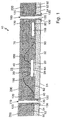
- the picture of the FIG. 1 shows a schematic view of a first non-inventive embodiment, comprising an IC package 10 with a semiconductor body 20 having a top 22 and a bottom 24.
- the semiconductor body 20 has a monolithic integrated circuit, not shown, with a first metallic contact surface 30 and a second metallic contact surface 40 on.
- the two contact surfaces 30 and 40 are formed on the upper side 22 of the semiconductor body 20.
- the integrated circuit is connected by means of printed conductors, not shown, to the two electrical contact surfaces 30 and 40. Furthermore, a carrier substrate 50 having an upper side 52 and a lower side 54 is provided. The semiconductor body 20 is frictionally connected to the underside 24 on the upper side 52 of the carrier substrate 50 by means of an adhesive bond 60 with the carrier substrate 50. Preferably, the adhesive bond 60 is formed as a double-sided adhesive film.
- the carrier substrate 50 has a first metal surface 70 and a first connection contact 80 and a second connection contact 90.
- the two connection contacts 80 and 90 comprise a first through hole 100 formed through the carrier substrate 50 and a second through hole 110 formed through the carrier substrate 50 in the manner of a hole.
- the two Through-holes 100 and 110 have a circular cross-section and are formed in an edge region of the carrier substrate 50.
- a first electronic component 118 is connected to the first metal surface 70 and to the first connection contact 80.
- the first connection contact 80 is connected to the first through-connection 100 and the second connection contact 90 is connected to the second through-connection 110; wherein on the inner sides of the two plated-through holes 100 and 110 of the respective terminal contact 80 and 90 is formed.
- the two connection contacts 80 and 90 form an edge surface 120 at both through-contacts on the upper side 52 of the carrier substrate 50 and an edge surface 130 on the underside 54 of the carrier substrate 50.
- the two edge surfaces 120 and 130 and the inner sides 135 are each formed integrally with the respective terminal contact 80 and 90.
- the two contact surfaces 30 and 40 are each connected by means of a bonding wire 150 to the second terminal contact 90 and the first terminal contact 80.
- the electrical contact surface 40 is connected to the first metal surface 70.
- the first component 118 is connected to the first metal surface 70 and to the first connection contact 80.
- the second contact surface 40 forms a series circuit with that of the first metal surface 70 and the first component 118 and the first connection contact 80.
- a potting compound 200 is formed, so that inter alia the bonding wires 150, the semiconductor body 20 and the first electronic component 118 are covered or encapsulated with potting compound 200.
- the underside 54 of the carrier substrate 50 and on the upper side 52 of the carrier substrate 50, the plated-through holes 100 and 110 are free of the potting compound 200 to ensure electrical contact with other modules.
- assemblies include parts of connectors included.
- the carrier substrate 50 is preferably in the form of a plate made of an electrically insulating material in one piece.
- the plate has a thickness below 2 mm, highest preferably a thickness below 0.5 mm.
- the IC package 10 has a parallelepiped shape.
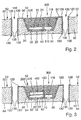
- FIG. 2 is a cross-sectional view of a second non-inventive embodiment of an IC package 10 is shown.
- the carrier substrate 50 has on the upper side 52, preferably in the middle, a trough-shaped formation 300 with a bottom region 310.
- the semiconductor body 20 and the electronic component 118 are arranged next to one another.
- the upper side 22 with the two contact surfaces 30 and 40 of the semiconductor body 20 now points in the direction of the bottom region 310.
- the two contact surfaces 30 and 40 are electrically connected to the second connection contact 90 and the first connection contact 80.
- connection contacts 70 and 80 have conductor track sections, wherein the track track sections extend over the edge of the trough to the first connection contact 100 and to the second connection contacts 110 and in each case to the associated connection contact. 100 and 110 interconnected.
- the trough is filled up with the potting compound 200, ie the remaining upper side 52 of the carrier substrate 50 and the underside 54 of the carrier substrate 50 have no potting compound.
- FIG. 3 is a cross-sectional view of a third non-inventive embodiment of an IC package 10 is shown.
- a further semiconductor body 400 is arranged on an adhesive layer 405 on the first semiconductor body 20, wherein the second semiconductor body 400 is connected to the connection contacts 100 and 110 by means of bond wires 150.
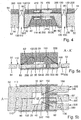
- FIG. 4 is a cross-sectional view of a fourth non-inventive embodiment of an IC package 10 is shown. following Only the differences from the second non-inventive embodiment, shown in the FIG. 2 , explained.
- the second semiconductor body 400 is arranged on the underside 54 of the carrier substrate 50 by means of the conductive adhesive. Furthermore, a second electronic component 410 is arranged on the underside 54 next to the second semiconductor body 400.
- the carrier substrate 50 is covered with the potting compound 200 so that the components 400 and 410 are also covered with potting compound 200 are.
- FIG. 5a Fig. 12 is a cross-sectional view taken along a line A - A 'of an embodiment of an IC package 10 according to the present invention.
- the carrier substrate 50 is now multi-piece and formed from a metal, in particular the first connection contact 80 is arranged on a separate part 500 of the carrier substrate 50.
- the first through-connection 100 is formed on the separate part 500.
- the bonding wire can be connected directly to the first connection contact 80 without the first connection contact 80 being formed as a side wall in the through-connection 100, 110.
- the potting compound 200 on the upper side 52 is arranged only on the region of the first semiconductor body 20 and the bonding wires 150 and likewise on the underside 54 is the central region of the carrier substrate 20.
- FIG. 5b is a plan view of the inventive embodiment of the IC package 10, shown in the FIG. 5a displayed.
- the FIG. 5a displayed on the upper side 22 of the Hableiter stresses 20 now four contact surfaces 30, 40, 501 and 502 and four separate connection contacts 80, 90, 580 and 590 are arranged, wherein all contact surfaces 30, 40, 501 and 502 by means of an associated bonding wire 150 with the individual connection contacts 80, 90, 580 and 590 are connected.
- the separate part 500 comprises the contact surfaces 80, 580 and 590.
- the vias 100 and 110 are provided in the individual connection regions for each pin. A formation of metallic pads on the carrier substrate is unnecessary.
Landscapes
- Engineering & Computer Science (AREA)
- Power Engineering (AREA)
- Computer Hardware Design (AREA)
- Microelectronics & Electronic Packaging (AREA)
- Physics & Mathematics (AREA)
- Condensed Matter Physics & Semiconductors (AREA)
- General Physics & Mathematics (AREA)
- Structures Or Materials For Encapsulating Or Coating Semiconductor Devices Or Solid State Devices (AREA)
- Geometry (AREA)
- Manufacturing & Machinery (AREA)
- Chemical & Material Sciences (AREA)
- Dispersion Chemistry (AREA)
- Wire Bonding (AREA)
- Structures For Mounting Electric Components On Printed Circuit Boards (AREA)
Applications Claiming Priority (2)
| Application Number | Priority Date | Filing Date | Title |
|---|---|---|---|
| DE102015000063.2A DE102015000063A1 (de) | 2015-01-12 | 2015-01-12 | IC-Gehäuse |
| EP16000047.7A EP3057129A1 (fr) | 2015-01-12 | 2016-01-12 | Boitier ic |
Related Parent Applications (1)
| Application Number | Title | Priority Date | Filing Date |
|---|---|---|---|
| EP16000047.7A Division EP3057129A1 (fr) | 2015-01-12 | 2016-01-12 | Boitier ic |
Publications (2)
| Publication Number | Publication Date |
|---|---|
| EP3133643A2 true EP3133643A2 (fr) | 2017-02-22 |
| EP3133643A3 EP3133643A3 (fr) | 2017-03-29 |
Family
ID=55129512
Family Applications (3)
| Application Number | Title | Priority Date | Filing Date |
|---|---|---|---|
| EP16002031.9A Withdrawn EP3133643A3 (fr) | 2015-01-12 | 2016-01-12 | Boitier ic |
| EP16002029.3A Withdrawn EP3133642A3 (fr) | 2015-01-12 | 2016-01-12 | Boitier ic |
| EP16000047.7A Withdrawn EP3057129A1 (fr) | 2015-01-12 | 2016-01-12 | Boitier ic |
Family Applications After (2)
| Application Number | Title | Priority Date | Filing Date |
|---|---|---|---|
| EP16002029.3A Withdrawn EP3133642A3 (fr) | 2015-01-12 | 2016-01-12 | Boitier ic |
| EP16000047.7A Withdrawn EP3057129A1 (fr) | 2015-01-12 | 2016-01-12 | Boitier ic |
Country Status (4)
| Country | Link |
|---|---|
| US (2) | US9893005B2 (fr) |
| EP (3) | EP3133643A3 (fr) |
| CN (2) | CN109346417A (fr) |
| DE (1) | DE102015000063A1 (fr) |
Families Citing this family (3)
| Publication number | Priority date | Publication date | Assignee | Title |
|---|---|---|---|---|
| JP6840466B2 (ja) | 2016-03-08 | 2021-03-10 | 株式会社アムコー・テクノロジー・ジャパン | 半導体パッケージ及び半導体パッケージの製造方法 |
| DE102017006406B4 (de) | 2017-07-07 | 2021-04-29 | Tdk-Micronas Gmbh | Gehäustes IC-Bauelement |
| DE102020000100B4 (de) | 2020-01-10 | 2024-09-19 | Tdk-Micronas Gmbh | Gehäustes IC-Bauelement |
Citations (2)
| Publication number | Priority date | Publication date | Assignee | Title |
|---|---|---|---|---|
| JPH01191455A (ja) * | 1988-01-27 | 1989-08-01 | Hitachi Ltd | 半導体装置 |
| DE102007032142A1 (de) | 2007-06-30 | 2009-01-02 | Robert Bosch Gmbh | Elektronikmodul und Verfahren zur Herstellung eines Elektronikmoduls |
Family Cites Families (26)
| Publication number | Priority date | Publication date | Assignee | Title |
|---|---|---|---|---|
| JPS6057222B2 (ja) * | 1980-03-26 | 1985-12-13 | シャープ株式会社 | フィルムキャリァ型半導体装置 |
| JPS58158955A (ja) | 1982-03-16 | 1983-09-21 | Toshiba Corp | 半導体集積回路装置 |
| JPH01196153A (ja) * | 1988-02-01 | 1989-08-07 | Oki Electric Ind Co Ltd | 樹脂封止半導体装置 |
| JPH04162656A (ja) | 1990-10-26 | 1992-06-08 | Hitachi Ltd | 半導体集積回路装置およびその実装構造 |
| JPH04280696A (ja) * | 1991-03-08 | 1992-10-06 | Hitachi Ltd | 高集積半導体装置 |
| JPH0563138A (ja) * | 1991-04-18 | 1993-03-12 | Hitachi Ltd | 半導体集積回路装置 |
| US5241454A (en) * | 1992-01-22 | 1993-08-31 | International Business Machines Corporation | Mutlilayered flexible circuit package |
| JPH05343602A (ja) * | 1992-06-11 | 1993-12-24 | Hitachi Ltd | 高集積半導体装置及びそれを用いた半導体モジュール |
| US5592025A (en) * | 1992-08-06 | 1997-01-07 | Motorola, Inc. | Pad array semiconductor device |
| KR0147259B1 (ko) * | 1994-10-27 | 1998-08-01 | 김광호 | 적층형 패키지 및 그 제조방법 |
| DE19515322C2 (de) | 1995-04-20 | 1997-12-04 | Brose Fahrzeugteile | Antriebsvorrichtung mit einem Elektromotor und einem den Motorstrom schaltenden Relais |
| JP2792494B2 (ja) * | 1996-01-17 | 1998-09-03 | 日本電気株式会社 | 集積回路の実装構造 |
| JP2001274324A (ja) * | 2000-03-24 | 2001-10-05 | Hitachi Chem Co Ltd | 積層型半導体装置用半導体搭載用基板、半導体装置及び積層型半導体装置 |
| TW511409B (en) * | 2000-05-16 | 2002-11-21 | Hitachi Aic Inc | Printed wiring board having cavity for mounting electronic parts therein and method for manufacturing thereof |
| US6885093B2 (en) * | 2002-02-28 | 2005-04-26 | Freescale Semiconductor, Inc. | Stacked die semiconductor device |
| US6798074B2 (en) * | 2002-03-04 | 2004-09-28 | Motorola, Inc. | Method of attaching a die to a substrate |
| US6911624B2 (en) * | 2002-08-23 | 2005-06-28 | Micron Technology, Inc. | Component installation, removal, and replacement apparatus and method |
| US20060097385A1 (en) * | 2004-10-25 | 2006-05-11 | Negley Gerald H | Solid metal block semiconductor light emitting device mounting substrates and packages including cavities and heat sinks, and methods of packaging same |
| US7378726B2 (en) * | 2005-12-28 | 2008-05-27 | Intel Corporation | Stacked packages with interconnecting pins |
| US7453154B2 (en) * | 2006-03-29 | 2008-11-18 | Delphi Technologies, Inc. | Carbon nanotube via interconnect |
| US7616451B2 (en) * | 2006-10-13 | 2009-11-10 | Stmicroelectronics S.R.L. | Semiconductor package substrate and method, in particular for MEMS devices |
| KR101424137B1 (ko) * | 2007-09-07 | 2014-08-04 | 삼성전자주식회사 | 리세스부를 갖는 수지기판을 구비하는 반도체 패키지 및그의 제조방법 |
| JP5341337B2 (ja) * | 2007-10-25 | 2013-11-13 | スパンション エルエルシー | 半導体装置及びその製造方法 |
| US8159052B2 (en) * | 2008-04-10 | 2012-04-17 | Semtech Corporation | Apparatus and method for a chip assembly including a frequency extending device |
| TWI414050B (zh) * | 2010-10-19 | 2013-11-01 | 聯京光電股份有限公司 | 封裝板與其製造方法 |
| US9337116B2 (en) * | 2010-10-28 | 2016-05-10 | Stats Chippac, Ltd. | Semiconductor device and method of forming stepped interposer for stacking and electrically connecting semiconductor die |
-
2015
- 2015-01-12 DE DE102015000063.2A patent/DE102015000063A1/de not_active Withdrawn
-
2016
- 2016-01-11 CN CN201811144119.0A patent/CN109346417A/zh not_active Withdrawn
- 2016-01-11 CN CN201610014083.9A patent/CN105789166B/zh active Active
- 2016-01-12 EP EP16002031.9A patent/EP3133643A3/fr not_active Withdrawn
- 2016-01-12 US US14/993,299 patent/US9893005B2/en active Active
- 2016-01-12 EP EP16002029.3A patent/EP3133642A3/fr not_active Withdrawn
- 2016-01-12 EP EP16000047.7A patent/EP3057129A1/fr not_active Withdrawn
-
2018
- 2018-01-05 US US15/863,245 patent/US10026684B2/en active Active
Patent Citations (2)
| Publication number | Priority date | Publication date | Assignee | Title |
|---|---|---|---|---|
| JPH01191455A (ja) * | 1988-01-27 | 1989-08-01 | Hitachi Ltd | 半導体装置 |
| DE102007032142A1 (de) | 2007-06-30 | 2009-01-02 | Robert Bosch Gmbh | Elektronikmodul und Verfahren zur Herstellung eines Elektronikmoduls |
Non-Patent Citations (1)
| Title |
|---|
| ANDREAS VEIGEL ET AL.: "Einpresstechnik - Entwicklung, Anwendung, Qualifizierung", 2009, EUGEN G. LEUZE VERLAG |
Also Published As
| Publication number | Publication date |
|---|---|
| US9893005B2 (en) | 2018-02-13 |
| US20160204055A1 (en) | 2016-07-14 |
| EP3057129A1 (fr) | 2016-08-17 |
| US20180130729A1 (en) | 2018-05-10 |
| US10026684B2 (en) | 2018-07-17 |
| CN109346417A (zh) | 2019-02-15 |
| EP3133642A2 (fr) | 2017-02-22 |
| EP3133642A3 (fr) | 2017-04-12 |
| EP3133643A3 (fr) | 2017-03-29 |
| CN105789166B (zh) | 2018-11-09 |
| CN105789166A (zh) | 2016-07-20 |
| DE102015000063A1 (de) | 2016-07-14 |
Similar Documents
| Publication | Publication Date | Title |
|---|---|---|
| DE19930308B4 (de) | Multichipmodul mit Silicium-Trägersubstrat | |
| DE69709176T2 (de) | Gegossene fassungen zur befestigung von elektronischen bauelementen | |
| DE102013201931B4 (de) | Laserbauelement und Verfahren zu seiner Herstellung | |
| DE102015115805B4 (de) | Elektronisches bauelement und verfahren zum herstellen eines elektronischen bauelements | |
| DE102013100701B4 (de) | Halbleitermodulanordnung und verfahren zur herstellung einer halbleitermodulanordnung | |
| DE4430798A1 (de) | Stanzgitter zur Verbindung von elektrischen Bauelementen | |
| DE102009000490A1 (de) | Einpressverbinder | |
| DE69216452T2 (de) | Halbleiteranordnung mit elektromagnetischer Abschirmung | |
| DE102010042987A1 (de) | Verfahren zum Herstellen einer elektrischen Schaltung und elektrische Schaltung | |
| EP3133643A2 (fr) | Boitier ic | |
| EP3066618B1 (fr) | Module de circuits intégrés pour différentes techniques de connexion | |
| DE112016000586B4 (de) | Schaltungsanordnung | |
| WO2008017556A2 (fr) | Boîtier moulé adapté à la technique de montage par pression | |
| DE4321592B4 (de) | Halbleitervorrichtungen sowie ein Chipauflage-Trägerteil und ein Tape-Carrier-Gehäuse hierfür | |
| WO2018188947A1 (fr) | Ensemble de contact électrique | |
| DE102013203759A1 (de) | Optoelektronisches Bauelement und elektronisches Gerät mit optoelektronischem Bauelement | |
| DE102016218970A1 (de) | Elektronikmodul und Verfahren zur Herstellung eines Elektronikmoduls | |
| EP0995235B1 (fr) | Contact pour de minuscules contacts de liaison et procede de production d'un contact | |
| DE102017006406B4 (de) | Gehäustes IC-Bauelement | |
| DE102015115819A1 (de) | Leiterbrückenelement sowie Bestückungsgurt und Leiterplatten mit einem solchen | |
| DE19914741A1 (de) | Leistungshalbleitermodul | |
| EP3646678A1 (fr) | Module électronique et procédé de fabrication d'un module électronique | |
| DE102016101757A1 (de) | Schaltungsmodul mit oberflächenmontierbaren unterlagsblöcken zum anschliessen einer leiterplatte | |
| DE10142118B4 (de) | Elektronisches Bauteil mit wenigstens zwei gestapelten Halbleiterchips sowie Verfahren zu seiner Herstellung | |
| DE102020000100B4 (de) | Gehäustes IC-Bauelement |
Legal Events
| Date | Code | Title | Description |
|---|---|---|---|
| PUAI | Public reference made under article 153(3) epc to a published international application that has entered the european phase |
Free format text: ORIGINAL CODE: 0009012 |
|
| STAA | Information on the status of an ep patent application or granted ep patent |
Free format text: STATUS: THE APPLICATION HAS BEEN PUBLISHED |
|
| AC | Divisional application: reference to earlier application |
Ref document number: 3057129 Country of ref document: EP Kind code of ref document: P |
|
| AK | Designated contracting states |
Kind code of ref document: A2 Designated state(s): AL AT BE BG CH CY CZ DE DK EE ES FI FR GB GR HR HU IE IS IT LI LT LU LV MC MK MT NL NO PL PT RO RS SE SI SK SM TR |
|
| PUAL | Search report despatched |
Free format text: ORIGINAL CODE: 0009013 |
|
| AK | Designated contracting states |
Kind code of ref document: A3 Designated state(s): AL AT BE BG CH CY CZ DE DK EE ES FI FR GB GR HR HU IE IS IT LI LT LU LV MC MK MT NL NO PL PT RO RS SE SI SK SM TR |
|
| RIC1 | Information provided on ipc code assigned before grant |
Ipc: H01L 23/31 20060101ALI20170221BHEP Ipc: H01L 23/495 20060101AFI20170221BHEP |
|
| RAP1 | Party data changed (applicant data changed or rights of an application transferred) |
Owner name: TDK-MICRONAS GMBH |
|
| STAA | Information on the status of an ep patent application or granted ep patent |
Free format text: STATUS: REQUEST FOR EXAMINATION WAS MADE |
|
| 17P | Request for examination filed |
Effective date: 20170703 |
|
| RBV | Designated contracting states (corrected) |
Designated state(s): AL AT BE BG CH CY CZ DE DK EE ES FI FR GB GR HR HU IE IS IT LI LT LU LV MC MK MT NL NO PL PT RO RS SE SI SK SM TR |
|
| STAA | Information on the status of an ep patent application or granted ep patent |
Free format text: STATUS: EXAMINATION IS IN PROGRESS |
|
| 17Q | First examination report despatched |
Effective date: 20171117 |
|
| STAA | Information on the status of an ep patent application or granted ep patent |
Free format text: STATUS: THE APPLICATION HAS BEEN WITHDRAWN |
|
| 18W | Application withdrawn |
Effective date: 20180424 |