EP3133643A2 - Integrated circuit housing - Google Patents
Integrated circuit housing Download PDFInfo
- Publication number
- EP3133643A2 EP3133643A2 EP16002031.9A EP16002031A EP3133643A2 EP 3133643 A2 EP3133643 A2 EP 3133643A2 EP 16002031 A EP16002031 A EP 16002031A EP 3133643 A2 EP3133643 A2 EP 3133643A2
- Authority
- EP
- European Patent Office
- Prior art keywords
- carrier substrate
- semiconductor body
- package
- connection
- potting compound
- Prior art date
- Legal status (The legal status is an assumption and is not a legal conclusion. Google has not performed a legal analysis and makes no representation as to the accuracy of the status listed.)
- Withdrawn
Links
Images
Classifications
-
- H10W70/635—
-
- H10W70/464—
-
- H10W70/421—
-
- H10W70/65—
-
- H10W74/014—
-
- H10W74/111—
-
- H10W76/47—
-
- H10W70/682—
-
- H10W72/0198—
-
- H10W72/072—
-
- H10W72/07232—
-
- H10W72/07236—
-
- H10W72/073—
-
- H10W72/354—
-
- H10W72/59—
-
- H10W72/877—
-
- H10W72/884—
-
- H10W72/932—
-
- H10W74/114—
-
- H10W90/724—
-
- H10W90/732—
-
- H10W90/734—
-
- H10W90/754—
-
- H10W90/756—
Definitions
- the invention relates to an IC package
- the object of the invention is to provide a device which further develops the prior art.
- an IC package with a semiconductor body wherein the semiconductor body has a monolithically integrated circuit and at least two metallic contact surfaces and the integrated circuit is interconnected by means of conductor tracks to the two electrical contact surfaces and the semiconductor body on a multi-piece and made of metal arranged carrier substrate and is non-positively connected to the carrier substrate.
- the carrier substrate has at least two connection contacts and the two connection contacts are connected to the two contact surfaces.
- the semiconductor body and at least part of an upper side and a lower side of the carrier substrate are covered with a potting compound, wherein the potting compound forms a part of the IC housing and a respective portion of the two connection contacts penetrate the potting compound of the IC housing, wherein the two connection contacts are arranged on the carrier substrate are.
- Each terminal contact forms with the lying below the respective terminal contact carrier substrate from a hole-like shape, wherein the respective hole-like shape is formed as a via, to provide an electrical connection with another electrical component.
- hole-like formation is a through opening in the carrier substrate is designated and the walls in the opening are metallically conductive, thereby forming an electrically conductive via, wherein the two terminal contacts are each arranged on different portions of the carrier substrate.
- the plated-through hole is sleeve-shaped.
- the IC package from the potting compound and the carrier substrate.
- the carrying capacity of the carrier substrate is sufficient to accommodate the terminal contacts and the vias before the IC package is formed by means of the potting compound.
- the term "lead frame" is also customary for the carrier substrate, namely in particular when the carrier substrate consists of a metal or of a plurality of metal strips.
- the IC housing can be electrically connected directly to a further component by means of a through-connection formed directly with the IC housing.
- a connection plane can be saved with the device according to the invention by inserting into the plated-through holes of the IC housing, preferably by means of a press-fit pin with a higher-order system such as a Connect plug or cable directly. This can increase the yield and reduce the costs of assembly.
- the carrier substrate comprises or consists of an electrically insulating material.
- the carrier substrate plastic compounds or metal-plastic compounds, for example in the form of injection molded parts so-called "molded interconnect devices".
- the terminal contacts are formed as metallic strips on the carrier substrate.
- the vias have a preferably circular cross-section. It is preferable that the aspect ratio between the length and the diameter of the via is at least greater than or equal to 1.
- the plated-through holes are positively and materially connected to the carrier substrate. This makes it possible to create particularly durable and low-resistance electrical connections.
- the contact surfaces are with a conductive adhesive or with a bonding wire or by means of a solder joint or by sintering or electrically connected by means of a thermocompression bond with the connection contacts.
- the carrier substrate it is also preferable to arrange on the carrier substrate another electronic component spaced apart from the semiconductor body and to cover both components in one process step with the same potting compound.
- An example of the two components are Hall sensors which are arranged either laterally or stapeiförmig within the IC housing.
- the carrier substrate is formed as a flat plate.
- the carrier substrate has a trough-shaped formation on an upper side, wherein the semiconductor body is arranged in a bottom region of the trough-shaped formation.
- all vias are formed in an edge region of the carrier substrate.
- one or more semiconductor bodies and / or one or more electronic components are arranged both on and under the carrier substrate.
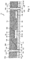
- the picture of the FIG. 1 shows a schematic view of a first non-inventive embodiment, comprising an IC package 10 with a semiconductor body 20 having a top 22 and a bottom 24.
- the semiconductor body 20 has a monolithic integrated circuit, not shown, with a first metallic contact surface 30 and a second metallic contact surface 40 on.
- the two contact surfaces 30 and 40 are formed on the upper side 22 of the semiconductor body 20.
- the integrated circuit is connected by means of printed conductors, not shown, to the two electrical contact surfaces 30 and 40. Furthermore, a carrier substrate 50 having an upper side 52 and a lower side 54 is provided. The semiconductor body 20 is frictionally connected to the underside 24 on the upper side 52 of the carrier substrate 50 by means of an adhesive bond 60 with the carrier substrate 50. Preferably, the adhesive bond 60 is formed as a double-sided adhesive film.
- the carrier substrate 50 has a first metal surface 70 and a first connection contact 80 and a second connection contact 90.
- the two connection contacts 80 and 90 comprise a first through hole 100 formed through the carrier substrate 50 and a second through hole 110 formed through the carrier substrate 50 in the manner of a hole.
- the two Through-holes 100 and 110 have a circular cross-section and are formed in an edge region of the carrier substrate 50.
- a first electronic component 118 is connected to the first metal surface 70 and to the first connection contact 80.
- the first connection contact 80 is connected to the first through-connection 100 and the second connection contact 90 is connected to the second through-connection 110; wherein on the inner sides of the two plated-through holes 100 and 110 of the respective terminal contact 80 and 90 is formed.
- the two connection contacts 80 and 90 form an edge surface 120 at both through-contacts on the upper side 52 of the carrier substrate 50 and an edge surface 130 on the underside 54 of the carrier substrate 50.
- the two edge surfaces 120 and 130 and the inner sides 135 are each formed integrally with the respective terminal contact 80 and 90.
- the two contact surfaces 30 and 40 are each connected by means of a bonding wire 150 to the second terminal contact 90 and the first terminal contact 80.
- the electrical contact surface 40 is connected to the first metal surface 70.
- the first component 118 is connected to the first metal surface 70 and to the first connection contact 80.
- the second contact surface 40 forms a series circuit with that of the first metal surface 70 and the first component 118 and the first connection contact 80.
- a potting compound 200 is formed, so that inter alia the bonding wires 150, the semiconductor body 20 and the first electronic component 118 are covered or encapsulated with potting compound 200.
- the underside 54 of the carrier substrate 50 and on the upper side 52 of the carrier substrate 50, the plated-through holes 100 and 110 are free of the potting compound 200 to ensure electrical contact with other modules.
- assemblies include parts of connectors included.
- the carrier substrate 50 is preferably in the form of a plate made of an electrically insulating material in one piece.
- the plate has a thickness below 2 mm, highest preferably a thickness below 0.5 mm.
- the IC package 10 has a parallelepiped shape.
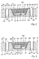
- FIG. 2 is a cross-sectional view of a second non-inventive embodiment of an IC package 10 is shown.
- the carrier substrate 50 has on the upper side 52, preferably in the middle, a trough-shaped formation 300 with a bottom region 310.
- the semiconductor body 20 and the electronic component 118 are arranged next to one another.
- the upper side 22 with the two contact surfaces 30 and 40 of the semiconductor body 20 now points in the direction of the bottom region 310.
- the two contact surfaces 30 and 40 are electrically connected to the second connection contact 90 and the first connection contact 80.
- connection contacts 70 and 80 have conductor track sections, wherein the track track sections extend over the edge of the trough to the first connection contact 100 and to the second connection contacts 110 and in each case to the associated connection contact. 100 and 110 interconnected.
- the trough is filled up with the potting compound 200, ie the remaining upper side 52 of the carrier substrate 50 and the underside 54 of the carrier substrate 50 have no potting compound.
- FIG. 3 is a cross-sectional view of a third non-inventive embodiment of an IC package 10 is shown.
- a further semiconductor body 400 is arranged on an adhesive layer 405 on the first semiconductor body 20, wherein the second semiconductor body 400 is connected to the connection contacts 100 and 110 by means of bond wires 150.
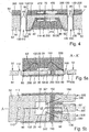
- FIG. 4 is a cross-sectional view of a fourth non-inventive embodiment of an IC package 10 is shown. following Only the differences from the second non-inventive embodiment, shown in the FIG. 2 , explained.
- the second semiconductor body 400 is arranged on the underside 54 of the carrier substrate 50 by means of the conductive adhesive. Furthermore, a second electronic component 410 is arranged on the underside 54 next to the second semiconductor body 400.
- the carrier substrate 50 is covered with the potting compound 200 so that the components 400 and 410 are also covered with potting compound 200 are.
- FIG. 5a Fig. 12 is a cross-sectional view taken along a line A - A 'of an embodiment of an IC package 10 according to the present invention.
- the carrier substrate 50 is now multi-piece and formed from a metal, in particular the first connection contact 80 is arranged on a separate part 500 of the carrier substrate 50.
- the first through-connection 100 is formed on the separate part 500.
- the bonding wire can be connected directly to the first connection contact 80 without the first connection contact 80 being formed as a side wall in the through-connection 100, 110.
- the potting compound 200 on the upper side 52 is arranged only on the region of the first semiconductor body 20 and the bonding wires 150 and likewise on the underside 54 is the central region of the carrier substrate 20.
- FIG. 5b is a plan view of the inventive embodiment of the IC package 10, shown in the FIG. 5a displayed.
- the FIG. 5a displayed on the upper side 22 of the Hableiter stresses 20 now four contact surfaces 30, 40, 501 and 502 and four separate connection contacts 80, 90, 580 and 590 are arranged, wherein all contact surfaces 30, 40, 501 and 502 by means of an associated bonding wire 150 with the individual connection contacts 80, 90, 580 and 590 are connected.
- the separate part 500 comprises the contact surfaces 80, 580 and 590.
- the vias 100 and 110 are provided in the individual connection regions for each pin. A formation of metallic pads on the carrier substrate is unnecessary.
Landscapes
- Engineering & Computer Science (AREA)
- Power Engineering (AREA)
- Computer Hardware Design (AREA)
- Microelectronics & Electronic Packaging (AREA)
- Physics & Mathematics (AREA)
- Condensed Matter Physics & Semiconductors (AREA)
- General Physics & Mathematics (AREA)
- Structures Or Materials For Encapsulating Or Coating Semiconductor Devices Or Solid State Devices (AREA)
- Geometry (AREA)
- Manufacturing & Machinery (AREA)
- Chemical & Material Sciences (AREA)
- Dispersion Chemistry (AREA)
- Wire Bonding (AREA)
- Structures For Mounting Electric Components On Printed Circuit Boards (AREA)
Abstract
IC-Gehäuse mit einem Halbleiterkörper, wobei der Halbleiterkörper eine monolithisch integrierte Schaltung und wenigstens zwei metallische Kontaktflächen aufweist und die integrierte Schaltung mittels Leiterbahnen mit den beiden elektrischen Kontaktflächen verschaltet ist und der Halbleiterkörper auf einem mehrstückigen und aus Metall ausgebildeten Trägersubstrat angeordnet und mit dem Trägersubstrat kraftschlüssig verbunden ist und das Trägersubstrat wenigstens zwei Anschlusskontakte aufweist und die beiden Anschlusskontakte mit den beiden Kontaktflächen verschaltet sind und der Halbleiterkörper und zumindest ein Teil einer Oberseite und einer Unterseite des Trägersubstrat mit einer Vergussmasse bedeckt sind, wobei die Vergussmasse einen Teil des IC Gehäuse ausbildet und jeweils ein Abschnitt der beiden Anschlusskontakte das IC Gehäuse durchdringt, wobei die beiden Anschlusskontakte auf dem Trägersubstrat angeordnet sind und jeder Anschlusskontakte und das unterhalb des jeweiligen Anschlusskontakte liegende Trägersubstrat eine lochartige Ausformung aufweisen, wobei die jeweilige lochartige Ausformung als Durchkontaktierung ausgebildet ist, um eine elektrische Verbindung mit einem weiteren elektrischen Bauteil bereitzustellen, wobei die beiden Anschlusskontakte jeweils auf unterschiedlichen Teilstücken des Trägersubstrats angeordnet sind.

Description
Aus der
Vor diesem Hintergrund besteht die Aufgabe der Erfindung darin, eine Vorrichtung anzugeben, die den Stand der Technik weiterbildet.Against this background, the object of the invention is to provide a device which further develops the prior art.
Die Aufgabe wird durch ein IC-Gehäuse mit den Merkmalen des Patentanspruchs 1 gelöst. Vorteilhafte Ausgestaltungen der Erfindung sind Gegenstand von Unteransprüchen.The object is achieved by an IC package having the features of patent claim 1. Advantageous embodiments of the invention are the subject of dependent claims.
Gemäß dem Gegenstand der Erfindung wird ein IC-Gehäuse mit einem Halbleiterkörper bereitgestellt, wobei der Halbleiterkörper eine monolithisch integrierte Schaltung und wenigstens zwei metallische Kontaktflächen aufweist und die integrierte Schaltung mittels Leiterbahnen mit den beiden elektrischen Kontaktflächen verschaltet ist und der Halbleiterkörper auf einem mehrstückig und aus Metall ausgebildeten Trägersubstrat angeordnet und mit dem Trägersubstrat kraftschlüssig verbunden ist.According to the subject matter of the invention, an IC package with a semiconductor body is provided, wherein the semiconductor body has a monolithically integrated circuit and at least two metallic contact surfaces and the integrated circuit is interconnected by means of conductor tracks to the two electrical contact surfaces and the semiconductor body on a multi-piece and made of metal arranged carrier substrate and is non-positively connected to the carrier substrate.
Das Trägersubstrat weist wenigstens zwei Anschlusskontakte auf und die beiden Anschlusskontakte sind mit den beiden Kontaktflächen verschaltet.The carrier substrate has at least two connection contacts and the two connection contacts are connected to the two contact surfaces.
Der Halbleiterkörper und zumindest ein Teil einer Oberseite und einer Unterseite des Trägersubstrats sind mit einer Vergussmasse bedeckt, wobei die Vergussmasse einen Teil des IC Gehäuses ausbildet und jeweils ein Abschnitt der beiden Anschlusskontakte die Vergussmasse des IC Gehäuses durchdringen, wobei die beiden Anschlusskontakte auf dem Trägersubstrat angeordnet sind.The semiconductor body and at least part of an upper side and a lower side of the carrier substrate are covered with a potting compound, wherein the potting compound forms a part of the IC housing and a respective portion of the two connection contacts penetrate the potting compound of the IC housing, wherein the two connection contacts are arranged on the carrier substrate are.
Jeder Anschlusskontakt bildet mit dem unterhalb des jeweiligen Anschlusskontakts liegenden Trägersubstrat eine lochartige Ausformung aus, wobei die jeweilige lochartige Ausformung als Durchkontaktierung ausgeformt ist, um eine elektrische Verbindung mit einem weiteren elektrischen Bauteil bereitzustellen.Each terminal contact forms with the lying below the respective terminal contact carrier substrate from a hole-like shape, wherein the respective hole-like shape is formed as a via, to provide an electrical connection with another electrical component.
Es sei angemerkt, dass unter dem Begriff lochartig Ausformung eine durchgehende Öffnung in dem Trägersubstrat bezeichnet ist und die Wände in der Öffnung metallisch leitfähig sind, um hierdurch eine elektrisch leitende Durchkontaktierung auszubilden, wobei die beiden Anschlusskontakte jeweils auf unterschiedlichen Teilstücken des Trägersubstrats angeordnet sind. Insbesondere ist die Durchkontaktierung hülsenartig ausgebildet.It should be noted that the term hole-like formation is a through opening in the carrier substrate is designated and the walls in the opening are metallically conductive, thereby forming an electrically conductive via, wherein the two terminal contacts are each arranged on different portions of the carrier substrate. In particular, the plated-through hole is sleeve-shaped.
Es versteht sich, dass es bevorzugt ist, das IC-Gehäuse aus der Vergussmasse und dem Trägersubstrat auszubilden. Alternativ ist auch bevorzugt, das Gehäuse ausschließlich mittels der Vergussmasse auszubilden, anders ausgedrückt die innenliegende Bauteile vollständig mit der Vergussmasse zu umschließen.It is understood that it is preferable to form the IC package from the potting compound and the carrier substrate. Alternatively, it is also preferred to form the housing exclusively by means of the potting compound, in other words to completely enclose the internal components with the potting compound.
Es versteht sich, dass die Tragfähigkeit des Trägersubstrats ausreichend ist, um die Anschlusskontakte und die Durchkontaktierungen aufzunehmen, bevor mittels der Vergussmasse das IC-Gehäuse ausgebildet wird. Es sei angemerkt, dass für das Trägersubstrat auch die Bezeichnung "Lead-frame" gebräuchlich ist, nämlich insbesondere dann, wenn das Trägersubstrat aus einem Metall bzw. aus mehreren Metallstreifen besteht.It is understood that the carrying capacity of the carrier substrate is sufficient to accommodate the terminal contacts and the vias before the IC package is formed by means of the potting compound. It should be noted that the term "lead frame" is also customary for the carrier substrate, namely in particular when the carrier substrate consists of a metal or of a plurality of metal strips.
Ein Vorteil der erfindungsgemäßen Vorrichtung ist es, dass das IC-Gehäuse unmittelbar mit einem weiteren Bauteil mittels einer unmittelbar mit dem IC-Gehäuse ausgebildeten Durchkontaktierung elektrisch verschalten lässt. Eine Montage des IC-Gehäuses auf einer Trägerplatine, wobei die Trägerplatine die Durchkontaktierungen enthält, entfällt. Anders ausgedrückt lässt sich mit der erfindungsgemäßen Vorrichtung eine Verbindungsebene einsparen, indem in die Durchkontaktierungen des IC-Gehäuses vorzugsweise mittels eines Einpressstiftes mit einem übergeordneten System wie beispielsweise einem Stecker oder Kabel unmittelbar verbinden lässt. Hierdurch lässt sich die Ausbeute erhöhen und die Fügungskosten reduzieren.One advantage of the device according to the invention is that the IC housing can be electrically connected directly to a further component by means of a through-connection formed directly with the IC housing. An assembly of the IC package on a carrier board, wherein the carrier board contains the vias omitted. In other words, a connection plane can be saved with the device according to the invention by inserting into the plated-through holes of the IC housing, preferably by means of a press-fit pin with a higher-order system such as a Connect plug or cable directly. This can increase the yield and reduce the costs of assembly.
In einer nicht erfindungsgemäßen Ausführung umfasst oder besteht das Trägersubstrat aus einem elektrisch isolierenden Material. Bevorzugt sind als Material das Trägersubstrat Kunststoffverbindungen oder Metall-Kunststoffverbindungen, beispielsweise in Form von Spritzgussteilen sogenannten "molded interconnect devices". Hierbei sind die Anschlusskontakte als metallische Streifen auf dem Trägersubstrat ausgebildet.In a non-inventive embodiment, the carrier substrate comprises or consists of an electrically insulating material. Preferably, as the material, the carrier substrate plastic compounds or metal-plastic compounds, for example in the form of injection molded parts so-called "molded interconnect devices". Here, the terminal contacts are formed as metallic strips on the carrier substrate.
Bei der erfindungsgemäßen Ausführung des Trägersubstrats erübrigt sich eine Ausbildung von metallischen Streifen auf der Oberfläche des Trägersubstrats, in dem bereits die Anschlusskontakte selbst aus einzelnen metallischen, jedoch zueinander isolierten Streifen ausgebildet sind.In the embodiment of the carrier substrate according to the invention, a formation of metallic strips on the surface of the carrier substrate, in which the terminal contacts themselves are formed of individual metallic but mutually insulated strips, is unnecessary.
Es ist bevorzugt, dass die Durchkontaktierungen einen vorzugsweise kreisförmigen Querschnitt aufweisen. Bevorzugst ist, dass das Aspekt Verhältnis zwischen der Länge und dem Durchmesser der Durchkontaktierung mindestens größer gleich 1 ist.It is preferred that the vias have a preferably circular cross-section. It is preferable that the aspect ratio between the length and the diameter of the via is at least greater than or equal to 1.
In die Durchkontaktierungen lassen sich sowohl Stifte einpressen als auch Stifte verlöten. Untersuchungen haben gezeigt, dass es vorteilhaft ist, in den Durchkontaktierungen an der Lochinnenseite eine metallische Oberfläche auszubilden, wobei die metallische Oberfläche als ein Teil des Außenkontakts ausgebildet ist und vorzugsweise einstückig mit dem Außen kontakt verbunden ist. In einer alternativen AusführungsformIn the vias can both press in pins and solder pins. Studies have shown that it is advantageous to form a metallic surface in the plated-through holes on the inner side of the hole, wherein the metallic surface is formed as a part of the outer contact and is preferably integrally connected to the outer contact. In an alternative embodiment
Bevorzugt ist es des Weiteren die Durchkontaktierungen kraft- und stoffschlüssig mit dem Trägersubstrat zu verbinden. Hierdurch lassen sich besonders haltbare und niederohmige elektrische Verbindungen schaffen.Furthermore, it is preferable for the plated-through holes to be positively and materially connected to the carrier substrate. This makes it possible to create particularly durable and low-resistance electrical connections.
In einer Ausführungsform sind die Kontaktflächen mit einem Leitkleber oder mit einem Bonddraht oder mittels einer Lötverbindung oder mittels Sintern oder mittels eines Thermokompressionsbonds mit den Anschlusskontakten elektrisch verschaltet.In one embodiment, the contact surfaces are with a conductive adhesive or with a bonding wire or by means of a solder joint or by sintering or electrically connected by means of a thermocompression bond with the connection contacts.
Auch ist es bevorzugt auf dem Trägersubstrat ein weiteres von dem Halbleiterkörper beabstandetes elektronisches Bauelement anzuordnen und beide Bauteile In einem Verfahrensschritt mit derselben Vergussmasse zu bedecken. Ein Beispiels für die beiden Bauelemente sind Hallsensoren welche entweder lateral oder stapeiförmig innerhalb des IC-Gehäuses angeordnet sind.It is also preferable to arrange on the carrier substrate another electronic component spaced apart from the semiconductor body and to cover both components in one process step with the same potting compound. An example of the two components are Hall sensors which are arranged either laterally or stapeiförmig within the IC housing.
In einer bevorzugten Weiterbildung ist das Trägersubstrat als eine plane Platte ausgebildet. In einer nicht erfindungsgemäßen Ausführungsform weist das Trägersubstrat an einer Oberseite eine wannenförmige Ausformung auf, wobei der der Halbleiterkörper in einem Bodenbereich der wannenförmigen Ausformung angeordnet ist.In a preferred embodiment, the carrier substrate is formed as a flat plate. In a non-inventive embodiment, the carrier substrate has a trough-shaped formation on an upper side, wherein the semiconductor body is arranged in a bottom region of the trough-shaped formation.
Vorzugsweise sind alle Durchkontaktierungen in einem Randbereich des Trägersubstrats ausgebildet. In einer alternativen Ausführungsform sind sowohl auf als auch unter dem Trägersubstrat ein oder mehrere Halbleiterkörper und / oder ein oder mehrere elektronische Bauteile angeordnet. Hierdurch lassen sich auf einfache und kostengünstige Weise Multichip-Lösungen herstellen ohne dass eine Trägerplatine benötigt wird.Preferably, all vias are formed in an edge region of the carrier substrate. In an alternative embodiment, one or more semiconductor bodies and / or one or more electronic components are arranged both on and under the carrier substrate. As a result, multichip solutions can be produced in a simple and cost-effective manner without the need for a carrier board.
Die Erfindung wird nachfolgend unter Bezugnahme auf die Zeichnungen näher erläutert. Hierbei werden gleichartige Teile mit identischen Bezeichnungen beschriftet. Die dargestellten Ausführungsformen sind stark schematisiert, d.h. die Abstände und die lateralen und die vertikalen Erstreckungen sind nicht maßstäblich und weisen, sofern nicht anders angegeben, auch keine ableitbaren geometrischen Relationen zueinander auf. Darin zeigt:
- Figur 1
- eine Querschnittsansicht auf eine erste nicht erfindungsgemäße Ausführungsform eines IC-Gehäuses,
- Figur 2
- eine Querschnittsansicht auf eine zweite nicht erfindungsgemäße Ausführungsform eines IC-Gehäuses,
- Figur 3
- eine Querschnittsansicht auf eine dritte nicht erfindungsgemäße Ausführungsform eines IC-Gehäuses,
- Figur 4
- eine Querschnittsansicht auf eine vierte nicht erfindungsgemäße Ausführungsform eines IC-Gehäuses,
- Figur 5a
- eine Querschnittsansicht auf eine erste erfindungsgemäße Ausführungsform eines IC-Gehäuses,
- Figur 5b
- eine Draufsicht entlang der Linie A-A' der erfindungsgemäßen Ausführungsform des IC-Gehäuses, dargestellt in der
Figur 5a .
- FIG. 1
- a cross-sectional view of a first non-inventive embodiment of an IC package,
- FIG. 2
- a cross-sectional view of a second non-inventive embodiment of an IC package,
- FIG. 3
- a cross-sectional view of a third non-inventive embodiment of an IC package,
- FIG. 4
- a cross-sectional view of a fourth non-inventive embodiment of an IC package,
- FIG. 5a
- a cross-sectional view of a first embodiment of an IC housing according to the invention,
- FIG. 5b
- a plan view along the line AA 'of the embodiment of the IC housing according to the invention, shown in the
FIG. 5a ,
Die Abbildung der
Die integrierte Schaltung ist mittels nicht dargestellten Leiterbahnen mit den beiden elektrischen Kontaktflächen 30 und 40 verschaltet. Des Weiteren ist ein Trägersubstrat 50 mit einer Oberseite 52 und einer Unterseite 54 vorgesehen. Der Halbleiterkörper 20 ist mit der Unterseite 24 auf der Oberseite 52 des Trägersubstrats 50 mittels einer Klebeverbindung 60 mit dem Trägersubstrat 50 kraftschlüssig verbunden. Vorzugsweise ist die Klebeverbindung 60 als eine doppeltseitig klebende Folie ausgebildet. Das Trägersubstrat 50 weist eine erste Metallfläche 70 und einen ersten Anschlusskontakt 80 und einen zweiten Anschlusskontakt 90 auf. Die beiden Anschlusskontakte 80 und 90 umfassen eine erste lochartig durch das Trägersubstrat 50 ausgebildete Durchkontaktierung 100 und eine zweite lochartig durch das Trägersubstrat 50 ausgebildete Durchkontaktierung 110 auf. Die beiden Durchkontaktierungen 100 und 110 weisen einen kreisförmigen Querschnitt auf und sind in einem Randbereich des Trägersubstrats 50 ausgebildet.The integrated circuit is connected by means of printed conductors, not shown, to the two electrical contact surfaces 30 and 40. Furthermore, a
Ein erstes elektronisches Bauelement 118 ist mit der ersten Metallfläche 70 und mit dem ersten Anschlusskontakt 80 verschaltet. Der erste Anschlusskontakt 80 ist mit der ersten Durchkontaktierung 100 und der zweite Anschlusskontakte 90 mit der zweiten Durchkontaktierung 110 verschaltet; wobei an den Innenseiten der beiden Durchkontaktierungen 100 und 110 der jeweilige Anschlusskontakt 80 und 90 ausgebildet ist. Hierbei bilden die beiden Anschlusskontakte 80 und 90 bei beiden Durchkontaktierungen an der Oberseite 52 des Trägersubstrat 50 eine Randfläche 120 und an der Unterseite 54 des Trägersubstrat 50 eine Randfläche 130 aus. Vorzugsweise sind die beiden Randflächen 120 und 130 und die Innenseiten 135 jeweils einstückig mit dem jeweiligen Anschlusskontakt 80 und 90 ausgebildet.A first
Die beiden Kontaktflächen 30 und 40 sind jeweils mittels eines Bonddrahtes 150 mit dem zweiten Anschlusskontakt 90 und dem ersten Anschlusskontakt 80 verschaltet. Hierbei ist vorliegend die elektrische Kontaktfläche 40 mit der ersten Metallfläche 70 verschaltet. Das erste Bauelement 118 ist mit der ersten Metallfläche 70 und mit dem ersten Anschlusskontakt 80 verschaltet. Anders ausgedrückt bildet die zweite Kontaktfläche 40 mit dem der ersten Metallfläche 70 und dem ersten Bauelement 118 und dem ersten Anschlusskontakt 80 eine Reihenschaltung aus. An der gesamten Oberseite 52 des Trägersubstrats 50 ist eine Vergussmasse 200 ausgebildet, so dass unter anderem die Bonddrähte 150, der Halbleiterkörper 20 und das erste elektronische Bauelement 118 mit Vergussmasse 200 abgedeckt bzw. umschlossen sind. Die Unterseite 54 des Trägersubstrats 50 sowie an der Oberseite 52 des Trägersubstrats 50 die Durchkontaktierungen 100 und 110 sind frei von der Vergussmasse 200, um eine elektrische Kontaktierung mit weiteren Baugruppen zu gewährleisten. Als Baugruppen sind unter anderem Teile von Steckverbindungen umfasst. Das Trägersubstrat 50 ist plattenförmig aus einem elektrisch isolierenden Material vorzugsweise einstückig ausgebildet. Vorzugsweise weist die Platte eine Dicke unterhalb 2 mm, höchst vorzugsweise eine Dicke unterhalb 0,5 mm auf. Ferner ist es bevorzugt, dass das IC-Gehäuse 10 eine quaderförmige Form aufweist.The two
In der
In der
In der
In der
Die Vergussmasse 200 auf der Oberseite 52 ist nur auf den Bereich des ersten Halbleiterkörpers 20 und der Bonddrähte 150 und ebenfalls auch an der Unterseite 54 ist ein den zentralen Bereich des Trägersubstrats 20 angeordnet.The
In der
Claims (8)
die beiden Anschlusskontakte (80, 90) mit den beiden Kontaktflächen (30, 40) verschaltet sind und der Halbleiterkörper (20) und zumindest ein Teil einer Oberseite (52) und einer Unterseite (54) des Trägersubstrats (50) mit einer Vergussmasse (200) bedeckt sind, wobei die Vergussmasse (200) einen Teil des IC Gehäuses (10) ausbildet, und jeweils ein Abschnitt der beiden Anschlusskontakte (80, 90) die Vergussmasse des IC Gehäuses (10) durchdringen
dadurch gekennzeichnet, dass
die beiden Anschlusskontakte (80, 90) auf dem Trägersubstrat (50) angeordnet sind und jeder Anschlusskontakt (80, 90) mit dem unterhalb des jeweiligen Anschlusskontakts (80, 90) liegenden Trägersubstrat (50) eine lochartige Ausformung ausbildet, wobei die jeweilige lochartige Ausformung als Durchkontaktierung (100, 110) ausgebildet ist, um eine elektrische Verbindung mit einem weiteren elektrischen Bauteil bereitzustellen, wobei die beiden Anschlusskontakte (80, 90) jeweils auf unterschiedlichen Teilstücken des Trägersubstrats angeordnet sind.IC package (10) having a semiconductor body (20), wherein the semiconductor body (20) has a monolithic integrated circuit and at least two metallic contact surfaces (30, 40) and the integrated circuit by means of printed conductors with the two electrical contact surfaces (30, 40) is connected and the semiconductor body (20) arranged on a multi-piece and made of metal carrier substrate (50) and non-positively connected to the carrier substrate (50) and the carrier substrate (50) has at least two terminal contacts (80, 90) and
the two connection contacts (80, 90) are connected to the two contact surfaces (30, 40) and the semiconductor body (20) and at least part of an upper side (52) and a lower side (54) of the carrier substrate (50) are provided with a potting compound (200 ), wherein the potting compound (200) forms a part of the IC housing (10), and in each case a portion of the two connection contacts (80, 90) penetrate the potting compound of the IC housing (10)
characterized in that
the two connection contacts (80, 90) are arranged on the carrier substrate (50) and each connection contact (80, 90) forms a hole-like formation with the carrier substrate (50) located below the respective connection contact (80, 90), the respective hole-like formation as a plated-through hole (100, 110) is formed in order to provide an electrical connection with a further electrical component, wherein the two terminal contacts (80, 90) are each arranged on different sections of the carrier substrate.
Applications Claiming Priority (2)
| Application Number | Priority Date | Filing Date | Title |
|---|---|---|---|
| DE102015000063.2A DE102015000063A1 (en) | 2015-01-12 | 2015-01-12 | IC package |
| EP16000047.7A EP3057129A1 (en) | 2015-01-12 | 2016-01-12 | Integrated circuit housing |
Related Parent Applications (1)
| Application Number | Title | Priority Date | Filing Date |
|---|---|---|---|
| EP16000047.7A Division EP3057129A1 (en) | 2015-01-12 | 2016-01-12 | Integrated circuit housing |
Publications (2)
| Publication Number | Publication Date |
|---|---|
| EP3133643A2 true EP3133643A2 (en) | 2017-02-22 |
| EP3133643A3 EP3133643A3 (en) | 2017-03-29 |
Family
ID=55129512
Family Applications (3)
| Application Number | Title | Priority Date | Filing Date |
|---|---|---|---|
| EP16002031.9A Withdrawn EP3133643A3 (en) | 2015-01-12 | 2016-01-12 | Integrated circuit housing |
| EP16002029.3A Withdrawn EP3133642A3 (en) | 2015-01-12 | 2016-01-12 | Integrated circuit housing |
| EP16000047.7A Withdrawn EP3057129A1 (en) | 2015-01-12 | 2016-01-12 | Integrated circuit housing |
Family Applications After (2)
| Application Number | Title | Priority Date | Filing Date |
|---|---|---|---|
| EP16002029.3A Withdrawn EP3133642A3 (en) | 2015-01-12 | 2016-01-12 | Integrated circuit housing |
| EP16000047.7A Withdrawn EP3057129A1 (en) | 2015-01-12 | 2016-01-12 | Integrated circuit housing |
Country Status (4)
| Country | Link |
|---|---|
| US (2) | US9893005B2 (en) |
| EP (3) | EP3133643A3 (en) |
| CN (2) | CN109346417A (en) |
| DE (1) | DE102015000063A1 (en) |
Families Citing this family (3)
| Publication number | Priority date | Publication date | Assignee | Title |
|---|---|---|---|---|
| JP6840466B2 (en) | 2016-03-08 | 2021-03-10 | 株式会社アムコー・テクノロジー・ジャパン | Semiconductor package and manufacturing method of semiconductor package |
| DE102017006406B4 (en) | 2017-07-07 | 2021-04-29 | Tdk-Micronas Gmbh | Packaged IC component |
| DE102020000100B4 (en) | 2020-01-10 | 2024-09-19 | Tdk-Micronas Gmbh | Packaged IC component |
Citations (2)
| Publication number | Priority date | Publication date | Assignee | Title |
|---|---|---|---|---|
| JPH01191455A (en) * | 1988-01-27 | 1989-08-01 | Hitachi Ltd | Semiconductor device |
| DE102007032142A1 (en) | 2007-06-30 | 2009-01-02 | Robert Bosch Gmbh | Electronic module and method for producing an electronic module |
Family Cites Families (26)
| Publication number | Priority date | Publication date | Assignee | Title |
|---|---|---|---|---|
| JPS6057222B2 (en) * | 1980-03-26 | 1985-12-13 | シャープ株式会社 | Film carrier type semiconductor device |
| JPS58158955A (en) | 1982-03-16 | 1983-09-21 | Toshiba Corp | Semiconductor integrated circuit device |
| JPH01196153A (en) * | 1988-02-01 | 1989-08-07 | Oki Electric Ind Co Ltd | Resin-sealed semiconductor device |
| JPH04162656A (en) | 1990-10-26 | 1992-06-08 | Hitachi Ltd | Semiconductor integrated circuit device and packaging structure thereof |
| JPH04280696A (en) * | 1991-03-08 | 1992-10-06 | Hitachi Ltd | High integrated semiconductor device |
| JPH0563138A (en) * | 1991-04-18 | 1993-03-12 | Hitachi Ltd | Semiconductor integrated circuit device |
| US5241454A (en) * | 1992-01-22 | 1993-08-31 | International Business Machines Corporation | Mutlilayered flexible circuit package |
| JPH05343602A (en) * | 1992-06-11 | 1993-12-24 | Hitachi Ltd | High density mounted semiconductor device and semiconductor module using the same |
| US5592025A (en) * | 1992-08-06 | 1997-01-07 | Motorola, Inc. | Pad array semiconductor device |
| KR0147259B1 (en) * | 1994-10-27 | 1998-08-01 | 김광호 | Stack type semiconductor package and method for manufacturing the same |
| DE19515322C2 (en) | 1995-04-20 | 1997-12-04 | Brose Fahrzeugteile | Drive device with an electric motor and a relay that switches the motor current |
| JP2792494B2 (en) * | 1996-01-17 | 1998-09-03 | 日本電気株式会社 | Integrated circuit mounting structure |
| JP2001274324A (en) * | 2000-03-24 | 2001-10-05 | Hitachi Chem Co Ltd | Semiconductor mounting substrate for stacked semiconductor device, semiconductor device, and stacked semiconductor device |
| TW511409B (en) * | 2000-05-16 | 2002-11-21 | Hitachi Aic Inc | Printed wiring board having cavity for mounting electronic parts therein and method for manufacturing thereof |
| US6885093B2 (en) * | 2002-02-28 | 2005-04-26 | Freescale Semiconductor, Inc. | Stacked die semiconductor device |
| US6798074B2 (en) * | 2002-03-04 | 2004-09-28 | Motorola, Inc. | Method of attaching a die to a substrate |
| US6911624B2 (en) * | 2002-08-23 | 2005-06-28 | Micron Technology, Inc. | Component installation, removal, and replacement apparatus and method |
| US20060097385A1 (en) * | 2004-10-25 | 2006-05-11 | Negley Gerald H | Solid metal block semiconductor light emitting device mounting substrates and packages including cavities and heat sinks, and methods of packaging same |
| US7378726B2 (en) * | 2005-12-28 | 2008-05-27 | Intel Corporation | Stacked packages with interconnecting pins |
| US7453154B2 (en) * | 2006-03-29 | 2008-11-18 | Delphi Technologies, Inc. | Carbon nanotube via interconnect |
| US7616451B2 (en) * | 2006-10-13 | 2009-11-10 | Stmicroelectronics S.R.L. | Semiconductor package substrate and method, in particular for MEMS devices |
| KR101424137B1 (en) * | 2007-09-07 | 2014-08-04 | 삼성전자주식회사 | Semiconductor package including resin substrate having recess, and method of fabricating the same |
| JP5341337B2 (en) * | 2007-10-25 | 2013-11-13 | スパンション エルエルシー | Semiconductor device and manufacturing method thereof |
| US8159052B2 (en) * | 2008-04-10 | 2012-04-17 | Semtech Corporation | Apparatus and method for a chip assembly including a frequency extending device |
| TWI414050B (en) * | 2010-10-19 | 2013-11-01 | 聯京光電股份有限公司 | Packaging board and manufacturing method thereof |
| US9337116B2 (en) * | 2010-10-28 | 2016-05-10 | Stats Chippac, Ltd. | Semiconductor device and method of forming stepped interposer for stacking and electrically connecting semiconductor die |
-
2015
- 2015-01-12 DE DE102015000063.2A patent/DE102015000063A1/en not_active Withdrawn
-
2016
- 2016-01-11 CN CN201811144119.0A patent/CN109346417A/en not_active Withdrawn
- 2016-01-11 CN CN201610014083.9A patent/CN105789166B/en active Active
- 2016-01-12 EP EP16002031.9A patent/EP3133643A3/en not_active Withdrawn
- 2016-01-12 US US14/993,299 patent/US9893005B2/en active Active
- 2016-01-12 EP EP16002029.3A patent/EP3133642A3/en not_active Withdrawn
- 2016-01-12 EP EP16000047.7A patent/EP3057129A1/en not_active Withdrawn
-
2018
- 2018-01-05 US US15/863,245 patent/US10026684B2/en active Active
Patent Citations (2)
| Publication number | Priority date | Publication date | Assignee | Title |
|---|---|---|---|---|
| JPH01191455A (en) * | 1988-01-27 | 1989-08-01 | Hitachi Ltd | Semiconductor device |
| DE102007032142A1 (en) | 2007-06-30 | 2009-01-02 | Robert Bosch Gmbh | Electronic module and method for producing an electronic module |
Non-Patent Citations (1)
| Title |
|---|
| ANDREAS VEIGEL ET AL.: "Einpresstechnik - Entwicklung, Anwendung, Qualifizierung", 2009, EUGEN G. LEUZE VERLAG |
Also Published As
| Publication number | Publication date |
|---|---|
| US9893005B2 (en) | 2018-02-13 |
| US20160204055A1 (en) | 2016-07-14 |
| EP3057129A1 (en) | 2016-08-17 |
| US20180130729A1 (en) | 2018-05-10 |
| US10026684B2 (en) | 2018-07-17 |
| CN109346417A (en) | 2019-02-15 |
| EP3133642A2 (en) | 2017-02-22 |
| EP3133642A3 (en) | 2017-04-12 |
| EP3133643A3 (en) | 2017-03-29 |
| CN105789166B (en) | 2018-11-09 |
| CN105789166A (en) | 2016-07-20 |
| DE102015000063A1 (en) | 2016-07-14 |
Similar Documents
| Publication | Publication Date | Title |
|---|---|---|
| DE19930308B4 (en) | Multichip module with silicon carrier substrate | |
| DE69709176T2 (en) | MOLDED VERSIONS FOR FIXING ELECTRONIC COMPONENTS | |
| DE102013201931B4 (en) | Laser component and method for its manufacture | |
| DE102015115805B4 (en) | ELECTRONIC COMPONENT AND METHOD OF MANUFACTURING AN ELECTRONIC COMPONENT | |
| DE102013100701B4 (en) | SEMICONDUCTOR MODULE ARRANGEMENT AND METHOD FOR MANUFACTURING A SEMICONDUCTOR MODULE ARRANGEMENT | |
| DE4430798A1 (en) | Lead frame for connecting electrical components | |
| DE102009000490A1 (en) | current fasteners | |
| DE69216452T2 (en) | Semiconductor device with electromagnetic shielding | |
| DE102010042987A1 (en) | Method for producing an electrical circuit and electrical circuit | |
| EP3133643A2 (en) | Integrated circuit housing | |
| EP3066618B1 (en) | Ic module for different connection technologies | |
| DE112016000586B4 (en) | Circuit arrangement | |
| WO2008017556A2 (en) | Molded housing used in force fit method | |
| DE4321592B4 (en) | Semiconductor devices and a chip support carrier part and a tape carrier housing therefor | |
| WO2018188947A1 (en) | Electrical contact assembly | |
| DE102013203759A1 (en) | Optoelectronic component and electronic device with optoelectronic component | |
| DE102016218970A1 (en) | Electronic module and method for producing an electronic module | |
| EP0995235B1 (en) | Contact for very small liaison contacts and method for producing a contact | |
| DE102017006406B4 (en) | Packaged IC component | |
| DE102015115819A1 (en) | Conductor bridge element and mounting belt and circuit boards with such | |
| DE19914741A1 (en) | Power semiconductor module has several external elements control connections connected with the internal wall of housing and also electrically connected with frame | |
| EP3646678A1 (en) | Electronic module and method for producing an electronic module | |
| DE102016101757A1 (en) | CIRCUIT MODULE WITH SURFACE MOUNTABLE SURFACE BLOCKS FOR CONNECTING A PCB | |
| DE10142118B4 (en) | Electronic component with at least two stacked semiconductor chips and method for its production | |
| DE102020000100B4 (en) | Packaged IC component |
Legal Events
| Date | Code | Title | Description |
|---|---|---|---|
| PUAI | Public reference made under article 153(3) epc to a published international application that has entered the european phase |
Free format text: ORIGINAL CODE: 0009012 |
|
| STAA | Information on the status of an ep patent application or granted ep patent |
Free format text: STATUS: THE APPLICATION HAS BEEN PUBLISHED |
|
| AC | Divisional application: reference to earlier application |
Ref document number: 3057129 Country of ref document: EP Kind code of ref document: P |
|
| AK | Designated contracting states |
Kind code of ref document: A2 Designated state(s): AL AT BE BG CH CY CZ DE DK EE ES FI FR GB GR HR HU IE IS IT LI LT LU LV MC MK MT NL NO PL PT RO RS SE SI SK SM TR |
|
| PUAL | Search report despatched |
Free format text: ORIGINAL CODE: 0009013 |
|
| AK | Designated contracting states |
Kind code of ref document: A3 Designated state(s): AL AT BE BG CH CY CZ DE DK EE ES FI FR GB GR HR HU IE IS IT LI LT LU LV MC MK MT NL NO PL PT RO RS SE SI SK SM TR |
|
| RIC1 | Information provided on ipc code assigned before grant |
Ipc: H01L 23/31 20060101ALI20170221BHEP Ipc: H01L 23/495 20060101AFI20170221BHEP |
|
| RAP1 | Party data changed (applicant data changed or rights of an application transferred) |
Owner name: TDK-MICRONAS GMBH |
|
| STAA | Information on the status of an ep patent application or granted ep patent |
Free format text: STATUS: REQUEST FOR EXAMINATION WAS MADE |
|
| 17P | Request for examination filed |
Effective date: 20170703 |
|
| RBV | Designated contracting states (corrected) |
Designated state(s): AL AT BE BG CH CY CZ DE DK EE ES FI FR GB GR HR HU IE IS IT LI LT LU LV MC MK MT NL NO PL PT RO RS SE SI SK SM TR |
|
| STAA | Information on the status of an ep patent application or granted ep patent |
Free format text: STATUS: EXAMINATION IS IN PROGRESS |
|
| 17Q | First examination report despatched |
Effective date: 20171117 |
|
| STAA | Information on the status of an ep patent application or granted ep patent |
Free format text: STATUS: THE APPLICATION HAS BEEN WITHDRAWN |
|
| 18W | Application withdrawn |
Effective date: 20180424 |