EP3130894B1 - Dispositif de détection d'anomalie de capteur et dispositif de détection - Google Patents
Dispositif de détection d'anomalie de capteur et dispositif de détection Download PDFInfo
- Publication number
- EP3130894B1 EP3130894B1 EP16168388.3A EP16168388A EP3130894B1 EP 3130894 B1 EP3130894 B1 EP 3130894B1 EP 16168388 A EP16168388 A EP 16168388A EP 3130894 B1 EP3130894 B1 EP 3130894B1
- Authority
- EP
- European Patent Office
- Prior art keywords
- operational amplifier
- input terminal
- inverting input
- bridge
- bridge midpoint
- Prior art date
- Legal status (The legal status is an assumption and is not a legal conclusion. Google has not performed a legal analysis and makes no representation as to the accuracy of the status listed.)
- Active
Links
Images


Classifications
-
- G—PHYSICS
- G01—MEASURING; TESTING
- G01D—MEASURING NOT SPECIALLY ADAPTED FOR A SPECIFIC VARIABLE; ARRANGEMENTS FOR MEASURING TWO OR MORE VARIABLES NOT COVERED IN A SINGLE OTHER SUBCLASS; TARIFF METERING APPARATUS; MEASURING OR TESTING NOT OTHERWISE PROVIDED FOR
- G01D18/00—Testing or calibrating apparatus or arrangements provided for in groups G01D1/00 - G01D15/00
-
- G—PHYSICS
- G01—MEASURING; TESTING
- G01D—MEASURING NOT SPECIALLY ADAPTED FOR A SPECIFIC VARIABLE; ARRANGEMENTS FOR MEASURING TWO OR MORE VARIABLES NOT COVERED IN A SINGLE OTHER SUBCLASS; TARIFF METERING APPARATUS; MEASURING OR TESTING NOT OTHERWISE PROVIDED FOR
- G01D3/00—Indicating or recording apparatus with provision for the special purposes referred to in the subgroups
- G01D3/08—Indicating or recording apparatus with provision for the special purposes referred to in the subgroups with provision for safeguarding the apparatus, e.g. against abnormal operation, against breakdown
-
- G—PHYSICS
- G01—MEASURING; TESTING
- G01R—MEASURING ELECTRIC VARIABLES; MEASURING MAGNETIC VARIABLES
- G01R17/00—Measuring arrangements involving comparison with a reference value, e.g. bridge
- G01R17/10—AC or DC measuring bridges
- G01R17/105—AC or DC measuring bridges for measuring impedance or resistance
-
- G—PHYSICS
- G01—MEASURING; TESTING
- G01R—MEASURING ELECTRIC VARIABLES; MEASURING MAGNETIC VARIABLES
- G01R31/00—Arrangements for testing electric properties; Arrangements for locating electric faults; Arrangements for electrical testing characterised by what is being tested not provided for elsewhere
- G01R31/28—Testing of electronic circuits, e.g. by signal tracer
- G01R31/282—Testing of electronic circuits specially adapted for particular applications not provided for elsewhere
- G01R31/2829—Testing of circuits in sensor or actuator systems
Definitions
- the present invention relates to an abnormality detection device that detects an abnormality of a detection signal caused by failure or the like, for example, in a sensor that acquires the detection signal from an output of a bridge circuit configured using sensor elements such as magnetic sensors.
- sensor elements of which impedance changes according to the physical amount of a detection target, such as a magnetic sensor, a temperature sensor, or a humidity sensor.
- the sensor elements are often used in the field of detection.
- a bridge circuit has been known as a circuit scheme for such detection.
- sinusoidal signals having a level corresponding to a rotation angle are output from one bridge midpoint and the other bridge midpoint, respectively. Since the two sinusoidal signals are opposite to each other in a phase, a sinusoidal signal having double amplitude is obtained by calculating a difference between the sinusoidal signals.
- a drift may occur with respect to a center level (offset level) of a fluctuation of the sinusoidal signal according to the rotation angle, for example, due to aging of characteristics, failure, or the like of the magnetic sensors. If the drift occurs, a drift component is included in the difference between the two sinusoidal signals output from the two bridge midpoints of the bridge circuit, in addition to the fluctuation of the sinusoidal signals according to the rotation angle, and exact detection of the rotation angle is not performed.
- An abnormality detection device for a sensor includes a bridge circuit including sensor elements of which the impedance changes according to a change in a physical amount of a detection target, a voltage at a first bridge midpoint and a voltage at a second bridge midpoint exhibiting a change of which the amount of change is equal and the polarity is opposite with respect to a predetermined intermediate voltage according to a change in the impedance of the sensor element; an operational amplifier; a feedback resistor provided between an output terminal and an inverting input terminal of the operational amplifier; a switch circuit that connects the first bridge midpoint to a non-inverting input terminal of the operational amplifier and connects the second bridge midpoint to the inverting input terminal of the operational amplifier in a first connection state, and connects the first bridge midpoint to the inverting input terminal of the operational amplifier and connects the second bridge midpoint to the non-inverting input terminal of the operational amplifier in a second connection state; and a determination unit that determines abnormality of a detection result
- the two bridge midpoints (the first bridge midpoint and the second bridge midpoint) of the bridge circuit and the input terminals (the inverting input terminal and the non-inverting input terminal) of the operational amplifier are connected through the switch circuit, it is possible to omit a buffer circuit for taking out a signal from the two bridge midpoints.
- An abnormality detection device for a sensor includes a bridge circuit including sensor elements of which the impedance changes according to a change in a physical amount of a detection target, a voltage at a first bridge midpoint and a voltage at a second bridge midpoint exhibiting a change of which the amount of change is equal and the polarity is opposite with respect to a predetermined intermediate voltage according to a change in the impedance of the sensor element; a first operational amplifier having a non-inverting input terminal connected to the first bridge midpoint and an inverting input terminal connected to the second bridge midpoint; a first feedback resistor provided between an output terminal and the inverting input terminal of the first operational amplifier; a second operational amplifier having a non-inverting input terminal connected to the second bridge midpoint and an inverting input terminal connected to the first bridge midpoint; a second feedback resistor provided between an output terminal and the inverting input terminal of the second operational amplifier; and a determination unit that determines abnormality of a detection result of the physical
- a sensor device includes a bridge circuit including sensor elements of which the impedance changes according to a change in a physical amount of a detection target, a voltage at a first bridge midpoint and a voltage at a second bridge midpoint exhibiting a change of which the amount of change is equal and the polarity is opposite with respect to a predetermined intermediate voltage according to a change in the impedance of the sensor element; an operational amplifier; a feedback resistor provided between an output terminal and an inverting input terminal of the operational amplifier; a switch circuit that connects the first bridge midpoint to the inverting input terminal of the operational amplifier and connects the second bridge midpoint to a non-inverting input terminal of the operational amplifier in a first connection state, and connects the first bridge midpoint to the non-inverting input terminal of the operational amplifier and connects the second bridge midpoint to the inverting input terminal of the operational amplifier in a second connection state; a detection signal acquisition unit that acquires a detection signal indicating a detection result of the
- a sensor device includes a bridge circuit including sensor elements of which the impedance changes according to a change in a physical amount of a detection target, a voltage at a first bridge midpoint and a voltage at a second bridge midpoint exhibiting a change of which the amount of change is equal and the polarity is opposite with respect to a predetermined intermediate voltage according to a change in the impedance of the sensor element; a first operational amplifier having a non-inverting input terminal connected to the first bridge midpoint and an inverting input terminal connected to the second bridge midpoint; a first feedback resistor provided between an output terminal and the inverting input terminal of the first operational amplifier; a second operational amplifier having a non-inverting input terminal connected to the second bridge midpoint and an inverting input terminal connected to the first bridge midpoint; a second feedback resistor provided between an output terminal and the inverting input terminal of the second operational amplifier; a detection signal acquisition unit that acquires a detection signal indicating a detection result of the physical amount
- the bridge circuit may include a first sensor element provided between a voltage supply line for supplying a predetermined voltage and the first bridge midpoint; a second sensor element provided between the first bridge midpoint and a reference potential; a third sensor element provided between the voltage supply line and the second bridge midpoint; and a fourth sensor element provided between the second bridge midpoint and the reference potential.
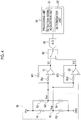
- Fig. 1 is a diagram illustrating an example of a configuration of a sensor device according to a first embodiment of the present invention.
- the sensor device illustrated in Fig. 1 includes a bridge circuit 10, a switch circuit 20, an operational amplifier 30, a feedback resistor Rf, a resistor Rb, an A/D conversion unit 40, and a processing unit 50.
- This sensor device operates as an abnormality detection device that detects an abnormality of a detection signal indicating a detection result of a physical amount due to, for example, generation of drift, in addition to an operation of acquiring the detection signal.
- the bridge circuit 10 includes sensor elements (R1 to R4) of which the impedance changes according to a change in a physical amount (for example, a magnetic field) of a detection target.
- a voltage at the first bridge midpoint and a voltage at the second bridge midpoint exhibit a change of which the amount of change is equal and the polarity is opposite with respect to a predetermined intermediate voltage Vofs according to a change in the impedance of the sensor elements (R1 to R4).
- a voltage at a first bridge midpoint N1 is "Vsp" and a voltage at a second bridge midpoints N2 is "Vsn”
- the voltages Vsp and Vsn are expressed by the following equations, respectively.
- Equations (1) and (2) "A" indicates a constant coefficient, and "sin ⁇ ” indicates a variable with a value from -1 to 1.
- a value of "sin ⁇ ” changes according to the detection result of the physical amount of the sensor elements (R1 to R4).
- the magnet and the sensor elements (R1 to R4) are arranged such that the voltages Vsp and Vsn show changes shown in Equations (1) and (2) according to an angle ⁇ of rotation.
- the bridge circuit 10 illustrated in the example of Fig. 1 includes a first sensor element R1, a second sensor element R2, a third sensor element R3, and a fourth sensor element R4.
- the first sensor element R1 is provided between a voltage supply line for supplying a power supply voltage Vcc and the first bridge midpoint N1.
- the second sensor element R2 is provided between the first bridge midpoint N1 and a reference potential GND.
- the third sensor element R3 is provided between the voltage supply line for the power supply voltage Vcc and the second bridge midpoint N2.
- the fourth sensor element R4 is provided between the second bridge midpoint N2 and the reference potential GND.
- the amounts of change in the impedance of the sensor elements (R1 to R4) according to the change in the physical amount of the detection target are substantially equal.
- Polarities of the change in the impedance according to the change in the physical amount of the detection target are opposite in the first sensor element R1 and the second sensor element R2, opposite in the third sensor element R3 and the fourth sensor element R4, the same in the first sensor element R1 and the fourth sensor element R4, and the same in the second sensor element R2 and the third sensor element R3.
- the impedance of the first sensor element R1 and the impedance of the second sensor element R2 are equal
- the impedance of the third sensor element R3 and the impedance of the fourth sensor element R4 are also equal.
- the voltages Vsp and Vsn become both equal to the intermediate voltage Vofs. Accordingly, the intermediate voltage Vofs becomes equal to a half voltage (Vcc/2) of the power supply voltage Vcc.
- the switch circuit 20 is a circuit for switching a connection between the two bridge midpoints (N1 and N2) of the bridge circuit 10 and two input terminals (an inverting input terminal and a non-inverting input terminal) of the operational amplifier 30, and having a first connection state and a second connection state.
- the switch circuit 20 connects the first bridge midpoint N1 to the non-inverting input terminal of the operational amplifier 30 and connects the second bridge midpoint N2 to the inverting input terminal of the operational amplifier 30 ( Fig. 2 ).
- the switch circuit 20 connects the first bridge midpoint N1 to the inverting input terminal of the operational amplifier 30 and connects the second bridge midpoint N2 to the non-inverting input terminal of the operational amplifier 30 ( Fig. 3 ).
- the feedback resistor Rf is connected between an output terminal of the operational amplifier 30 and the inverting input terminal.
- the resistor Rb is provided in a path of a current flowing between a node to which the switch circuit 20 and one terminal of the feedback resistor Rf are connected and the inverting input terminal of the operational amplifier 30.
- This resistor Rb is intended to reduce an offset voltage of the operational amplifier 30 which is generated due to an influence of a minute input current flowing in the inverting input terminal and the non-inverting input terminal of the operational amplifier 30.
- a resistance value of the resistor Rb is set such that impedance of a circuit connected to the inverting input terminal of the operational amplifier 30 and impedance of a circuit connected to the non-inverting input terminal of the operational amplifier 30 are approximate to each other.
- the A/D conversion unit 40 converts an output signal of the operational amplifier 30 from an analog signal to a digital signal.
- the processing unit 50 is a circuit that generally controls an entire operation of the sensor device.
- the processing unit 50 controls a switching operation of the switch circuit 20 and a conversion operation of the A/D conversion unit 40 so that respective output signals in a first connection state ( Fig. 2 ) and a second connection state ( Fig. 3 ) of the operational amplifier 30 are obtained in a case in which a predetermined command is given from a high-level device (not illustrated) or at a periodic timing set in advance.
- the processing unit 50 includes a computer that executes processing according to an instruction code of a program stored in a memory, or a logic circuit (for example, ASIC) according to dedicated hardware. Entire processing of the processing unit 50 may be executed by the computer or at least a part of the processing may be executed by the logic circuit of hardware.
- the processing unit 50 is a block that processes the output signal of the operational amplifier 30 converted Into the digital signal by the A/D conversion unit 40, and includes a detection signal acquisition unit 51 and a determination unit 52.
- the detection signal acquisition unit 51 acquires a detection signal indicating a detection result of the physical amount based on a difference between the output signal of the operational amplifier 30 in the first connection state ( Fig. 2 ) and the output signal of the operational amplifier 30 in the second connection state ( Fig. 3 ).
- the determination unit 52 determines an abnormality of the detection signal acquired by the detection signal acquisition unit 51 based on a sum of the output signal of the operational amplifier 30 in the first connection state ( Fig. 2 ) and the output signal of the operational amplifier 30 in the second connection state ( Fig. 3 ).
- G1 in Equation (3) indicates a voltage gain determined by the respective resistance values of the sensor elements R1 and R2 of the bridge circuit 10 and the feedback resistor Rf.
- G2 in Equation (4) indicates a voltage gain determined by the respective resistance values of the sensor elements R3 and R4 of the bridge circuit 10 and the feedback resistor Rf. If the resistance values of the sensor elements R1, R2, R3, and R4 are “R1”, “R2”, “R3”, and “R4", respectively, and the resistance value of the feedback resistor Rf is "Rf", the voltage gains G1 and G2 are expressed by the following equations, respectively.
- G 1 Rf ⁇ R 1 + R 2 / R 1 ⁇ R 2
- G 2 Rf ⁇ R 3 + R 4 / R 3 ⁇ R 4
- a signal of a result of subtracting the output signal Vi2 from the output signal Vi1 is a signal which is in proportional to a change "sin ⁇ " in a physical amount detected in the sensor elements (R1 to R4).
- the detection signal acquisition unit 51 acquires the signal of the subtraction result shown in Equation (11) as a detection signal.
- a result of adding the output signal Vi1 and the output signal Vi2 becomes substantially a constant value.
- the determination unit 52 determines whether or not the result of adding the output signal Vi1 and the output signal Vi2 is included in a predetermined normal range having the power supply voltage Vcc as a center value, and determines that the detection signal acquired by the detection signal acquisition unit 51 is normal in a case in which the addition result is included in the normal range.
- Equation (1) of the voltage Vsp is changed as shown in Equation (1A) below.
- Vsp Vofs + A ⁇ sin ⁇ + ⁇
- Equation (11A) an error component derived from the drift voltage ⁇ is included in the detection signal acquired in the detection signal acquisition unit 51. Therefore, the detection signal does not correctly represent a change "sin ⁇ " in the physical amount detected in the sensor elements (R1 to R4).
- the drift voltage ⁇ is included in the output signal Vi1A the result of adding the output signal Vi1 and the output signal Vi2 becomes a voltage separated from the supply voltage Vcc by the drift voltage ⁇ , as compared with the time of normality (Equation (12)). Therefore, if the drift voltage ⁇ increases beyond a certain limit, the result of adding the output signal Vi1 and the output signal Vi2 deviates from a predetermined normal range in which the power supply voltage Vcc is a center value, and the determination unit 52 determines that the detection signal acquired by the detection signal acquisition unit 51 is abnormal.
- the two input terminals (the inverting input terminal and the non-inverting input terminal) of the operational amplifier 30 in which the output voltage is fed back to the inverting input terminal via the feedback resistor Rf, and the two bridge midpoints (N1 and N2) of the bridge circuit 10 are connected via the switch circuit 20.
- the detection signal indicating the detection result of the physical amount of the sensor elements (R1 to R4) is acquired based on the difference between the output signal Vi1 of the operational amplifier 30 in a case in which the switch circuit 20 is in the first connection state ( Fig. 2 ) and the output signal Vi2 of the operational amplifier 30 in a case in which the switch circuit 20 is in the second connection state ( Fig. 3 ), and the abnormality of the detection signal is determined based on the sum of the output signal Vi1 and the output signal Vi2.
- the buffer circuit for taking out the signal from the two bridge midpoints (N1 and N2) of the bridge circuit 10 can be omitted, it is possible to simplify the circuit configuration.
- the sensor device according to the first embodiment described above generates the output signals (Vi1 and Vi2) of two patterns by switching the connection between one operational amplifier 30, in which the output voltage is fed back to the inverting input terminal via the feedback resistor Rf, and the bridge circuit 10 using the switch circuit 20.
- the sensor device according to the second embodiment generates the same output signal of two patterns as that in the first embodiment, using two operational amplifiers.
- Fig. 4 is a diagram illustrating an example of a configuration of a sensor device according to the second embodiment.
- the sensor device illustrated in Fig. 4 includes a bridge circuit 10, a first operational amplifier 31 and a second operational amplifier 32, a first feedback resistor Rf1 and a second feedback resistor Rf2, resistors Rb1 and Rb2, a switch circuit 60, an A/D conversion unit 40, and a processing unit 50.
- a bridge circuit 10 since the bridge circuit 10, the A/D conversion unit 40, and the processing unit 50 are the same as those in the sensor device illustrated in Fig. 1 , other components will be described hereinafter.
- a non-inverting input terminal is connected to a first bridge midpoint N1, and an inverting input terminal is connected to a second bridge midpoint N2.
- a non-inverting input terminal is connected to the second bridge midpoint N2, and an inverting input terminal is connected to the first bridge midpoint N1.
- the first feedback resistor Rf1 is provided between an output terminal and the inverting input terminal of the first operational amplifier 31.
- the second feedback resistor Rf2 is provided between an output terminal and the inverting input terminal of the second operational amplifier 32.
- the first feedback resistor Rf1 and the second feedback resistor Rf2 have a substantially equal resistance value.
- the first feedback resistor Rf1 and the second feedback resistor Rf2 have a resistance value sufficiently greater than those of resistors (R1 to R4) of the bridge circuit 10.
- the resistor Rb1 is provided in a path of a current flowing between a node to which the second bridge midpoint N2 and one terminal of the feedback resistor Rf1 are connected and the inverting input terminal of the first operational amplifier 31.
- the resistor Rb2 is provided in a path of a current flowing between a node to which the first bridge midpoint N1 and one terminal of the feedback resistor Rf2 are connected and the inverting input terminal of the second operational amplifier 32. Functions of the resistors Rb1 and Rb2 are the same as that of the resistor Rb in Fig. 1 .
- the switch circuit 60 selects one of an output signal Vi1 of the first operational amplifier 31 and an output signal Vi2 of the second operational amplifier 32 and inputs the output signal to the A/D conversion unit 40.
- the output signal Vi1 of the first operational amplifier 31 and the output signal Vi2 of the second operational amplifier 32 are input to the A/D conversion unit 40 via the switch circuit 60, are respectively converted into digital signals, and then, are input to a detection signal acquisition unit 51 and a determination unit 52 of the processing unit 50.
- a detection signal is acquired based on a difference between the output signal Vi1 and the output signal Vi2.
- the determination unit 52 abnormality of the detection signal is determined based on a sum of the output signal Vi1 and the output signal Vi2.
- the bridge circuit 10 includes four sensor elements (R1 to R4) has been described in the above-described embodiments, some of the four sensor elements (R1 to R4) may be replaced with resistors having fixed resistance in other embodiments of the present invention.
- A/D conversion units may be provided in the outputs of the two operational amplifiers (31 and 32), respectively, in other embodiments of the present invention.
- the signal processing of the detection signal acquisition unit 51 and the determination unit 52 is performed by a digital circuit in the above-described embodiments, the signal processing may be performed by an analog circuit in other embodiments of the present invention.
Claims (5)
- Dispositif de détection d'anomalie pour capteur, comprenant :un circuit en pont (10) comprenant des éléments capteurs dont l'impédance varie en fonction des variations d'une grandeur physique d'une cible de détection, une tension en un premier point milieu de pont (N1) et une tension en un second point milieu de pont (N2) présentant des variations, dont la quantité de variation est égale et la polarité est opposée, par rapport à une tension intermédiaire prédéterminée, en fonction des variations de l'impédance de l'élément capteur ;un amplificateur opérationnel (30) ;une résistance de rétroaction (Rf) disposée entre une borne de sortie et une borne d'entrée inverseuse de l'amplificateur opérationnel (30) ;un circuit de commutation (20) qui connecte le premier point milieu de pont (N1) à une borne d'entrée non inverseuse de l'amplificateur opérationnel (30) et connecte le second point milieu de pont (N2) à la borne d'entrée inverseuse de l'amplificateur opérationnel (30) dans un premier état de connexion, et connecte le premier point milieu de pont (N1) à la borne d'entrée inverseuse de l'amplificateur opérationnel (30) et connecte le second point milieu de pont (N2) à la borne d'entrée non inverseuse de l'amplificateur opérationnel (30) dans un second état de connexion ; etune unité de détermination (52) qui détermine une anomalie du résultat de détection de la grandeur physique acquis à partir d'une sortie du circuit en pont (10) sur la base d'une somme d'un signal de sortie de l'amplificateur opérationnel (30) dans le premier état de connexion et d'un signal de sortie de l'amplificateur opérationnel (30) dans le second état de connexion.
- Dispositif de détection d'anomalie pour capteur, comprenant :un circuit en pont (10) comprenant des éléments capteurs dont l'impédance varie en fonction des variations d'une grandeur physique d'une cible de détection, une tension en un premier point milieu de pont (N1) et une tension en un second point milieu de pont (N2) présentant des variations, dont la quantité de variation est égale et la polarité est opposée, par rapport à une tension intermédiaire prédéterminée, en fonction des variations de l'impédance de l'élément capteur ;un premier amplificateur opérationnel (31) comportant une borne d'entrée non inverseuse connectée au premier point milieu de pont (N1) et une borne d'entrée inverseuse connectée au second point milieu de pont (N2) ;une première résistance de rétroaction (Rf1) disposée entre une borne de sortie et la borne d'entrée inverseuse du premier amplificateur opérationnel (31) ;un second amplificateur opérationnel (32) comportant une borne d'entrée non inverseuse connectée au second point milieu de pont (N2) et une borne d'entrée inverseuse connectée au premier point milieu de pont (N1) ;une seconde résistance de rétroaction (Rf2) disposée entre une borne de sortie et la borne d'entrée inverseuse du second amplificateur opérationnel (32) ; etune unité de détermination (52) qui détermine une anomalie du résultat de détection de la grandeur physique acquis à partir d'une sortie du circuit en pont (10) sur la base d'une somme d'un signal de sortie du premier amplificateur opérationnel (31) et d'un signal de sortie du second amplificateur opérationnel (32).
- Dispositif capteur, comprenant :un circuit en pont (10) comprenant des éléments capteurs dont l'impédance varie en fonction des variations d'une grandeur physique d'une cible de détection, une tension en un premier point milieu de pont (N1) et une tension en un second point milieu de pont (N2) présentant des variations, dont la quantité de variation est égale et la polarité est opposée, par rapport à une tension intermédiaire prédéterminée, en fonction des variations de l'impédance de l'élément capteur ;un amplificateur opérationnel (30) ;une résistance de rétroaction (Rf) disposée entre une borne de sortie et une borne d'entrée inverseuse de l'amplificateur opérationnel (30) ;un circuit de commutation (20) qui connecte le premier point milieu de pont (N1) à la borne d'entrée inverseuse de l'amplificateur opérationnel (30) et connecte le second point milieu de pont (N2) à une borne d'entrée non inverseuse de l'amplificateur opérationnel (30) dans un premier état de connexion, et connecte le premier point milieu de pont (N1) à la borne d'entrée non inverseuse de l'amplificateur opérationnel (30) et connecte le second point milieu de pont (N2) à la borne d'entrée inverseuse de l'amplificateur opérationnel (30) dans un second état de connexion ;une unité d'acquisition de signal de détection (51) qui acquiert un signal de détection indiquant un résultat de détection de la grandeur physique sur la base d'une différence entre un signal de sortie de l'amplificateur opérationnel (30) dans le premier état de connexion et un signal de sortie de l'amplificateur opérationnel (30) dans le second état de connexion ; etune unité de détermination (52) qui détermine une anomalie du signal de détection sur la base d'une somme du signal de sortie de l'amplificateur opérationnel (30) dans le premier état de connexion et du signal de sortie de l'amplificateur opérationnel (30) dans le second état de connexion.
- Dispositif capteur, comprenant :un circuit en pont (10) comprenant des éléments capteurs dont l'impédance varie en fonction des variations d'une grandeur physique d'une cible de détection, une tension en un premier point milieu de pont (N1) et une tension en un second point milieu de pont (N2) présentant des variations, dont la quantité de variation est égale et la polarité est opposée, par rapport à une tension intermédiaire prédéterminée, en fonction des variations de l'impédance de l'élément capteur ;un premier amplificateur opérationnel (31) comportant une borne d'entrée non inverseuse connectée au premier point milieu de pont (N1) et une borne d'entrée inverseuse connectée au second point milieu de pont (N2) ;une première résistance de rétroaction (Rf1) disposée entre une borne de sortie et la borne d'entrée inverseuse du premier amplificateur opérationnel (31) ;un second amplificateur opérationnel (32) comportant une borne d'entrée non inverseuse connectée au second point milieu de pont (N2) et une borne d'entrée inverseuse connectée au premier point milieu de pont (N1) ;une seconde résistance de rétroaction (Rf2) disposée entre une borne de sortie et la borne d'entrée inverseuse du second amplificateur opérationnel (32) ;une unité d'acquisition de signal de détection (51) qui acquiert un signal de détection indiquant un résultat de détection de la grandeur physique sur la base d'une différence entre un signal de sortie du premier amplificateur opérationnel (31) et un signal de sortie du second amplificateur opérationnel (32) ; etune unité de détermination (52) qui détermine une anomalie du signal de détection sur la base d'une somme du signal de sortie du premier amplificateur opérationnel (31) et du signal de sortie du second amplificateur opérationnel (32).
- Dispositif capteur selon l'une quelconque des revendications 1 à 4,
dans lequel le circuit en pont (10) comprend :un premier élément capteur (R1) disposé entre une ligne d'alimentation en tension destinée à fournir une tension prédéterminée et le premier point milieu de pont(N1);un deuxième élément capteur (R2) disposé entre le premier point milieu de pont (N1) et un potentiel de référence ;un troisième élément capteur (R3) disposé entre la ligne d'alimentation en tension et le second point milieu de pont (N2) ; etun quatrième élément capteur (R4) disposé entre le second point milieu de pont (N2) et le potentiel de référence.
Applications Claiming Priority (1)
| Application Number | Priority Date | Filing Date | Title |
|---|---|---|---|
| JP2015105413A JP6386970B2 (ja) | 2015-05-25 | 2015-05-25 | センサの異常検出装置及びセンサ装置 |
Publications (3)
| Publication Number | Publication Date |
|---|---|
| EP3130894A2 EP3130894A2 (fr) | 2017-02-15 |
| EP3130894A3 EP3130894A3 (fr) | 2017-02-22 |
| EP3130894B1 true EP3130894B1 (fr) | 2017-09-13 |
Family
ID=55953007
Family Applications (1)
| Application Number | Title | Priority Date | Filing Date |
|---|---|---|---|
| EP16168388.3A Active EP3130894B1 (fr) | 2015-05-25 | 2016-05-04 | Dispositif de détection d'anomalie de capteur et dispositif de détection |
Country Status (2)
| Country | Link |
|---|---|
| EP (1) | EP3130894B1 (fr) |
| JP (1) | JP6386970B2 (fr) |
Families Citing this family (1)
| Publication number | Priority date | Publication date | Assignee | Title |
|---|---|---|---|---|
| EP3401646B1 (fr) * | 2017-05-09 | 2020-04-15 | Melexis Technologies SA | Vérification d'erreur de capteur à pont |
Family Cites Families (15)
| Publication number | Priority date | Publication date | Assignee | Title |
|---|---|---|---|---|
| US3976987A (en) * | 1975-08-29 | 1976-08-24 | Square D Company | Dual channel dynamic line isolation monitor |
| JPH0618202A (ja) * | 1992-07-02 | 1994-01-25 | Toshiba Corp | 非接触形変位計測回路 |
| US6422088B1 (en) * | 1999-09-24 | 2002-07-23 | Denso Corporation | Sensor failure or abnormality detecting system incorporated in a physical or dynamic quantity detecting apparatus |
| JP4617545B2 (ja) * | 1999-10-13 | 2011-01-26 | 株式会社デンソー | センサの異常検出回路及び物理量検出装置 |
| JP2005049097A (ja) | 2003-07-29 | 2005-02-24 | Alps Electric Co Ltd | 故障検出回路 |
| DE10347038A1 (de) * | 2003-10-07 | 2005-05-25 | Zentrum Mikroelektronik Dresden Ag | Verfahren und Schaltungsanordnung zur Ermittlung der Alterung von Sensoren |
| JP4749132B2 (ja) * | 2005-11-21 | 2011-08-17 | 富士通セミコンダクター株式会社 | センサ検出装置及びセンサ |
| JP5161433B2 (ja) * | 2006-05-16 | 2013-03-13 | 株式会社東海理化電機製作所 | センサ装置 |
| JP2008175660A (ja) * | 2007-01-18 | 2008-07-31 | Yaskawa Electric Corp | 異常検出装置および異常検出部を備えた位置検出器 |
| JP4675993B2 (ja) * | 2008-08-22 | 2011-04-27 | 株式会社東海理化電機製作所 | 異常検出回路 |
| JP2010048717A (ja) * | 2008-08-22 | 2010-03-04 | Tokai Rika Co Ltd | 位置検出装置 |
| JP5075930B2 (ja) * | 2010-02-19 | 2012-11-21 | 本田技研工業株式会社 | 電荷変化型センサの出力回路 |
| JP5375796B2 (ja) * | 2010-11-05 | 2013-12-25 | 株式会社デンソー | 回転角検出装置、および、これを用いた電動パワーステアリング装置 |
| JP6110639B2 (ja) * | 2012-11-16 | 2017-04-05 | 旭化成エレクトロニクス株式会社 | センサ閾値決定回路 |
| JP6056482B2 (ja) * | 2013-01-08 | 2017-01-11 | 株式会社ジェイテクト | 回転角センサの異常検出装置 |
-
2015
- 2015-05-25 JP JP2015105413A patent/JP6386970B2/ja active Active
-
2016
- 2016-05-04 EP EP16168388.3A patent/EP3130894B1/fr active Active
Non-Patent Citations (1)
| Title |
|---|
| None * |
Also Published As
| Publication number | Publication date |
|---|---|
| JP2016217972A (ja) | 2016-12-22 |
| EP3130894A3 (fr) | 2017-02-22 |
| JP6386970B2 (ja) | 2018-09-05 |
| EP3130894A2 (fr) | 2017-02-15 |
Similar Documents
| Publication | Publication Date | Title |
|---|---|---|
| KR101919256B1 (ko) | 전류 측정 동안 참조 전류에 의한 전류 센서들의 캘리브레이션 | |
| US10156589B2 (en) | Sensor module that switches plural sensors capable of measuring different ranges to extend dynamic range | |
| EP1922554B1 (fr) | Circuit de mesure de courant et procede de diagnostic d'un defaut s'y produisant | |
| EP3022737B1 (fr) | Circuit de détection de courant à étalonnage décalé | |
| US9128127B2 (en) | Sensor device | |
| JP2010060434A (ja) | 電圧検出装置 | |
| EP3139186A1 (fr) | Circuit de capteur | |
| JP2019509491A (ja) | マルチチャネルシステムのためのクロストーク較正 | |
| US20160349132A1 (en) | Physical quantity detector | |
| EP3130894B1 (fr) | Dispositif de détection d'anomalie de capteur et dispositif de détection | |
| AU2012214000A1 (en) | Device and method for evaluating signals of load cells with strain gauges | |
| CN109564139B (zh) | 传感器装置 | |
| JP6718284B2 (ja) | 信号処理回路、クーロンカウンタ回路、電子機器 | |
| JP4840087B2 (ja) | A/d変換方式 | |
| CN108982991B (zh) | 用于电容式加速度传感器的分析处理电路以及用于探测加速度的设备 | |
| US9285809B2 (en) | Current source with active common mode rejection | |
| JP5851316B2 (ja) | 電圧検出装置 | |
| US10393800B2 (en) | Circuit arrangement | |
| US9817034B2 (en) | Measuring device | |
| JP6315273B2 (ja) | 絶縁状態測定装置 | |
| JP4103789B2 (ja) | 保護制御装置 | |
| WO2021205942A1 (fr) | Circuit de traitement de signal et dispositif de détection de charge | |
| US10371723B2 (en) | Current sensor for biomedical measurements | |
| JP6732679B2 (ja) | 電流検出回路 | |
| JPS63271171A (ja) | 電源診断方式 |
Legal Events
| Date | Code | Title | Description |
|---|---|---|---|
| PUAI | Public reference made under article 153(3) epc to a published international application that has entered the european phase |
Free format text: ORIGINAL CODE: 0009012 |
|
| PUAL | Search report despatched |
Free format text: ORIGINAL CODE: 0009013 |
|
| AK | Designated contracting states |
Kind code of ref document: A2 Designated state(s): AL AT BE BG CH CY CZ DE DK EE ES FI FR GB GR HR HU IE IS IT LI LT LU LV MC MK MT NL NO PL PT RO RS SE SI SK SM TR |
|
| AX | Request for extension of the european patent |
Extension state: BA ME |
|
| AK | Designated contracting states |
Kind code of ref document: A3 Designated state(s): AL AT BE BG CH CY CZ DE DK EE ES FI FR GB GR HR HU IE IS IT LI LT LU LV MC MK MT NL NO PL PT RO RS SE SI SK SM TR |
|
| AX | Request for extension of the european patent |
Extension state: BA ME |
|
| RIC1 | Information provided on ipc code assigned before grant |
Ipc: G01D 18/00 20060101ALI20170119BHEP Ipc: G01D 5/18 20060101AFI20170119BHEP |
|
| REG | Reference to a national code |
Ref country code: DE Ref legal event code: R079 Ref document number: 602016000381 Country of ref document: DE Free format text: PREVIOUS MAIN CLASS: G01D0005180000 Ipc: G01D0018000000 |
|
| 17P | Request for examination filed |
Effective date: 20170310 |
|
| GRAP | Despatch of communication of intention to grant a patent |
Free format text: ORIGINAL CODE: EPIDOSNIGR1 |
|
| RBV | Designated contracting states (corrected) |
Designated state(s): AL AT BE BG CH CY CZ DE DK EE ES FI FR GB GR HR HU IE IS IT LI LT LU LV MC MK MT NL NO PL PT RO RS SE SI SK SM TR |
|
| RIC1 | Information provided on ipc code assigned before grant |
Ipc: G01D 3/08 20060101ALI20170329BHEP Ipc: G01D 18/00 20060101AFI20170329BHEP |
|
| INTG | Intention to grant announced |
Effective date: 20170420 |
|
| GRAS | Grant fee paid |
Free format text: ORIGINAL CODE: EPIDOSNIGR3 |
|
| GRAA | (expected) grant |
Free format text: ORIGINAL CODE: 0009210 |
|
| AK | Designated contracting states |
Kind code of ref document: B1 Designated state(s): AL AT BE BG CH CY CZ DE DK EE ES FI FR GB GR HR HU IE IS IT LI LT LU LV MC MK MT NL NO PL PT RO RS SE SI SK SM TR |
|
| REG | Reference to a national code |
Ref country code: GB Ref legal event code: FG4D |
|
| REG | Reference to a national code |
Ref country code: CH Ref legal event code: EP |
|
| REG | Reference to a national code |
Ref country code: IE Ref legal event code: FG4D |
|
| REG | Reference to a national code |
Ref country code: AT Ref legal event code: REF Ref document number: 928610 Country of ref document: AT Kind code of ref document: T Effective date: 20171015 |
|
| REG | Reference to a national code |
Ref country code: DE Ref legal event code: R096 Ref document number: 602016000381 Country of ref document: DE |
|
| REG | Reference to a national code |
Ref country code: NL Ref legal event code: MP Effective date: 20170913 |
|
| REG | Reference to a national code |
Ref country code: LT Ref legal event code: MG4D |
|
| PG25 | Lapsed in a contracting state [announced via postgrant information from national office to epo] |
Ref country code: FI Free format text: LAPSE BECAUSE OF FAILURE TO SUBMIT A TRANSLATION OF THE DESCRIPTION OR TO PAY THE FEE WITHIN THE PRESCRIBED TIME-LIMIT Effective date: 20170913 Ref country code: HR Free format text: LAPSE BECAUSE OF FAILURE TO SUBMIT A TRANSLATION OF THE DESCRIPTION OR TO PAY THE FEE WITHIN THE PRESCRIBED TIME-LIMIT Effective date: 20170913 Ref country code: LT Free format text: LAPSE BECAUSE OF FAILURE TO SUBMIT A TRANSLATION OF THE DESCRIPTION OR TO PAY THE FEE WITHIN THE PRESCRIBED TIME-LIMIT Effective date: 20170913 Ref country code: SE Free format text: LAPSE BECAUSE OF FAILURE TO SUBMIT A TRANSLATION OF THE DESCRIPTION OR TO PAY THE FEE WITHIN THE PRESCRIBED TIME-LIMIT Effective date: 20170913 Ref country code: NO Free format text: LAPSE BECAUSE OF FAILURE TO SUBMIT A TRANSLATION OF THE DESCRIPTION OR TO PAY THE FEE WITHIN THE PRESCRIBED TIME-LIMIT Effective date: 20171213 |
|
| REG | Reference to a national code |
Ref country code: AT Ref legal event code: MK05 Ref document number: 928610 Country of ref document: AT Kind code of ref document: T Effective date: 20170913 |
|
| PG25 | Lapsed in a contracting state [announced via postgrant information from national office to epo] |
Ref country code: ES Free format text: LAPSE BECAUSE OF FAILURE TO SUBMIT A TRANSLATION OF THE DESCRIPTION OR TO PAY THE FEE WITHIN THE PRESCRIBED TIME-LIMIT Effective date: 20170913 Ref country code: BG Free format text: LAPSE BECAUSE OF FAILURE TO SUBMIT A TRANSLATION OF THE DESCRIPTION OR TO PAY THE FEE WITHIN THE PRESCRIBED TIME-LIMIT Effective date: 20171213 Ref country code: LV Free format text: LAPSE BECAUSE OF FAILURE TO SUBMIT A TRANSLATION OF THE DESCRIPTION OR TO PAY THE FEE WITHIN THE PRESCRIBED TIME-LIMIT Effective date: 20170913 Ref country code: RS Free format text: LAPSE BECAUSE OF FAILURE TO SUBMIT A TRANSLATION OF THE DESCRIPTION OR TO PAY THE FEE WITHIN THE PRESCRIBED TIME-LIMIT Effective date: 20170913 Ref country code: GR Free format text: LAPSE BECAUSE OF FAILURE TO SUBMIT A TRANSLATION OF THE DESCRIPTION OR TO PAY THE FEE WITHIN THE PRESCRIBED TIME-LIMIT Effective date: 20171214 |
|
| PG25 | Lapsed in a contracting state [announced via postgrant information from national office to epo] |
Ref country code: NL Free format text: LAPSE BECAUSE OF FAILURE TO SUBMIT A TRANSLATION OF THE DESCRIPTION OR TO PAY THE FEE WITHIN THE PRESCRIBED TIME-LIMIT Effective date: 20170913 |
|
| PG25 | Lapsed in a contracting state [announced via postgrant information from national office to epo] |
Ref country code: CZ Free format text: LAPSE BECAUSE OF FAILURE TO SUBMIT A TRANSLATION OF THE DESCRIPTION OR TO PAY THE FEE WITHIN THE PRESCRIBED TIME-LIMIT Effective date: 20170913 Ref country code: PL Free format text: LAPSE BECAUSE OF FAILURE TO SUBMIT A TRANSLATION OF THE DESCRIPTION OR TO PAY THE FEE WITHIN THE PRESCRIBED TIME-LIMIT Effective date: 20170913 |
|
| REG | Reference to a national code |
Ref country code: FR Ref legal event code: PLFP Year of fee payment: 3 |
|
| PG25 | Lapsed in a contracting state [announced via postgrant information from national office to epo] |
Ref country code: AT Free format text: LAPSE BECAUSE OF FAILURE TO SUBMIT A TRANSLATION OF THE DESCRIPTION OR TO PAY THE FEE WITHIN THE PRESCRIBED TIME-LIMIT Effective date: 20170913 Ref country code: SM Free format text: LAPSE BECAUSE OF FAILURE TO SUBMIT A TRANSLATION OF THE DESCRIPTION OR TO PAY THE FEE WITHIN THE PRESCRIBED TIME-LIMIT Effective date: 20170913 Ref country code: EE Free format text: LAPSE BECAUSE OF FAILURE TO SUBMIT A TRANSLATION OF THE DESCRIPTION OR TO PAY THE FEE WITHIN THE PRESCRIBED TIME-LIMIT Effective date: 20170913 Ref country code: IT Free format text: LAPSE BECAUSE OF FAILURE TO SUBMIT A TRANSLATION OF THE DESCRIPTION OR TO PAY THE FEE WITHIN THE PRESCRIBED TIME-LIMIT Effective date: 20170913 Ref country code: IS Free format text: LAPSE BECAUSE OF FAILURE TO SUBMIT A TRANSLATION OF THE DESCRIPTION OR TO PAY THE FEE WITHIN THE PRESCRIBED TIME-LIMIT Effective date: 20180113 Ref country code: SK Free format text: LAPSE BECAUSE OF FAILURE TO SUBMIT A TRANSLATION OF THE DESCRIPTION OR TO PAY THE FEE WITHIN THE PRESCRIBED TIME-LIMIT Effective date: 20170913 |
|
| REG | Reference to a national code |
Ref country code: DE Ref legal event code: R097 Ref document number: 602016000381 Country of ref document: DE |
|
| PLBE | No opposition filed within time limit |
Free format text: ORIGINAL CODE: 0009261 |
|
| STAA | Information on the status of an ep patent application or granted ep patent |
Free format text: STATUS: NO OPPOSITION FILED WITHIN TIME LIMIT |
|
| PG25 | Lapsed in a contracting state [announced via postgrant information from national office to epo] |
Ref country code: DK Free format text: LAPSE BECAUSE OF FAILURE TO SUBMIT A TRANSLATION OF THE DESCRIPTION OR TO PAY THE FEE WITHIN THE PRESCRIBED TIME-LIMIT Effective date: 20170913 |
|
| 26N | No opposition filed |
Effective date: 20180614 |
|
| REG | Reference to a national code |
Ref country code: BE Ref legal event code: MM Effective date: 20180531 |
|
| PG25 | Lapsed in a contracting state [announced via postgrant information from national office to epo] |
Ref country code: MC Free format text: LAPSE BECAUSE OF FAILURE TO SUBMIT A TRANSLATION OF THE DESCRIPTION OR TO PAY THE FEE WITHIN THE PRESCRIBED TIME-LIMIT Effective date: 20170913 |
|
| REG | Reference to a national code |
Ref country code: DE Ref legal event code: R082 Ref document number: 602016000381 Country of ref document: DE Representative=s name: SCHMITT-NILSON SCHRAUD WAIBEL WOHLFROM PATENTA, DE Ref country code: DE Ref legal event code: R081 Ref document number: 602016000381 Country of ref document: DE Owner name: ALPS ALPINE CO., LTD., JP Free format text: FORMER OWNER: ALPS ELECTRIC CO., LTD., TOKYO, JP |
|
| REG | Reference to a national code |
Ref country code: IE Ref legal event code: MM4A |
|
| PG25 | Lapsed in a contracting state [announced via postgrant information from national office to epo] |
Ref country code: LU Free format text: LAPSE BECAUSE OF NON-PAYMENT OF DUE FEES Effective date: 20180504 |
|
| PG25 | Lapsed in a contracting state [announced via postgrant information from national office to epo] |
Ref country code: IE Free format text: LAPSE BECAUSE OF NON-PAYMENT OF DUE FEES Effective date: 20180504 |
|
| PG25 | Lapsed in a contracting state [announced via postgrant information from national office to epo] |
Ref country code: BE Free format text: LAPSE BECAUSE OF NON-PAYMENT OF DUE FEES Effective date: 20180531 |
|
| REG | Reference to a national code |
Ref country code: CH Ref legal event code: PL |
|
| PG25 | Lapsed in a contracting state [announced via postgrant information from national office to epo] |
Ref country code: LI Free format text: LAPSE BECAUSE OF NON-PAYMENT OF DUE FEES Effective date: 20190531 Ref country code: CH Free format text: LAPSE BECAUSE OF NON-PAYMENT OF DUE FEES Effective date: 20190531 Ref country code: MT Free format text: LAPSE BECAUSE OF NON-PAYMENT OF DUE FEES Effective date: 20180504 |
|
| PG25 | Lapsed in a contracting state [announced via postgrant information from national office to epo] |
Ref country code: TR Free format text: LAPSE BECAUSE OF FAILURE TO SUBMIT A TRANSLATION OF THE DESCRIPTION OR TO PAY THE FEE WITHIN THE PRESCRIBED TIME-LIMIT Effective date: 20170913 |
|
| PG25 | Lapsed in a contracting state [announced via postgrant information from national office to epo] |
Ref country code: PT Free format text: LAPSE BECAUSE OF FAILURE TO SUBMIT A TRANSLATION OF THE DESCRIPTION OR TO PAY THE FEE WITHIN THE PRESCRIBED TIME-LIMIT Effective date: 20170913 |
|
| PG25 | Lapsed in a contracting state [announced via postgrant information from national office to epo] |
Ref country code: CY Free format text: LAPSE BECAUSE OF FAILURE TO SUBMIT A TRANSLATION OF THE DESCRIPTION OR TO PAY THE FEE WITHIN THE PRESCRIBED TIME-LIMIT Effective date: 20170913 Ref country code: RO Free format text: LAPSE BECAUSE OF FAILURE TO SUBMIT A TRANSLATION OF THE DESCRIPTION OR TO PAY THE FEE WITHIN THE PRESCRIBED TIME-LIMIT Effective date: 20170913 Ref country code: HU Free format text: LAPSE BECAUSE OF FAILURE TO SUBMIT A TRANSLATION OF THE DESCRIPTION OR TO PAY THE FEE WITHIN THE PRESCRIBED TIME-LIMIT; INVALID AB INITIO Effective date: 20160504 Ref country code: MK Free format text: LAPSE BECAUSE OF NON-PAYMENT OF DUE FEES Effective date: 20170913 |
|
| PG25 | Lapsed in a contracting state [announced via postgrant information from national office to epo] |
Ref country code: AL Free format text: LAPSE BECAUSE OF FAILURE TO SUBMIT A TRANSLATION OF THE DESCRIPTION OR TO PAY THE FEE WITHIN THE PRESCRIBED TIME-LIMIT Effective date: 20170913 |
|
| PGFP | Annual fee paid to national office [announced via postgrant information from national office to epo] |
Ref country code: FR Payment date: 20200522 Year of fee payment: 5 |
|
| PGFP | Annual fee paid to national office [announced via postgrant information from national office to epo] |
Ref country code: GB Payment date: 20200527 Year of fee payment: 5 |
|
| PG25 | Lapsed in a contracting state [announced via postgrant information from national office to epo] |
Ref country code: SI Free format text: LAPSE BECAUSE OF NON-PAYMENT OF DUE FEES Effective date: 20180504 |
|
| GBPC | Gb: european patent ceased through non-payment of renewal fee |
Effective date: 20210504 |
|
| PG25 | Lapsed in a contracting state [announced via postgrant information from national office to epo] |
Ref country code: GB Free format text: LAPSE BECAUSE OF NON-PAYMENT OF DUE FEES Effective date: 20210504 |
|
| PG25 | Lapsed in a contracting state [announced via postgrant information from national office to epo] |
Ref country code: FR Free format text: LAPSE BECAUSE OF NON-PAYMENT OF DUE FEES Effective date: 20210531 |
|
| PGFP | Annual fee paid to national office [announced via postgrant information from national office to epo] |
Ref country code: DE Payment date: 20230519 Year of fee payment: 8 |