EP3115995B1 - Dispositif de mémoire à semi-conducteur, procédé de réparation de colonne défectueuse et procédé de réglage de ses informations redondantes - Google Patents
Dispositif de mémoire à semi-conducteur, procédé de réparation de colonne défectueuse et procédé de réglage de ses informations redondantes Download PDFInfo
- Publication number
- EP3115995B1 EP3115995B1 EP16178002.8A EP16178002A EP3115995B1 EP 3115995 B1 EP3115995 B1 EP 3115995B1 EP 16178002 A EP16178002 A EP 16178002A EP 3115995 B1 EP3115995 B1 EP 3115995B1
- Authority
- EP
- European Patent Office
- Prior art keywords
- column
- col
- bad
- columns
- redundant
- Prior art date
- Legal status (The legal status is an assumption and is not a legal conclusion. Google has not performed a legal analysis and makes no representation as to the accuracy of the status listed.)
- Active
Links
Images


Classifications
-
- G—PHYSICS
- G11—INFORMATION STORAGE
- G11C—STATIC STORES
- G11C29/00—Checking stores for correct operation ; Subsequent repair; Testing stores during standby or offline operation
- G11C29/70—Masking faults in memories by using spares or by reconfiguring
- G11C29/78—Masking faults in memories by using spares or by reconfiguring using programmable devices
- G11C29/785—Masking faults in memories by using spares or by reconfiguring using programmable devices with redundancy programming schemes
-
- G—PHYSICS
- G11—INFORMATION STORAGE
- G11C—STATIC STORES
- G11C29/00—Checking stores for correct operation ; Subsequent repair; Testing stores during standby or offline operation
- G11C29/70—Masking faults in memories by using spares or by reconfiguring
- G11C29/78—Masking faults in memories by using spares or by reconfiguring using programmable devices
- G11C29/80—Masking faults in memories by using spares or by reconfiguring using programmable devices with improved layout
- G11C29/808—Masking faults in memories by using spares or by reconfiguring using programmable devices with improved layout using a flexible replacement scheme
-
- G—PHYSICS
- G11—INFORMATION STORAGE
- G11C—STATIC STORES
- G11C29/00—Checking stores for correct operation ; Subsequent repair; Testing stores during standby or offline operation
- G11C29/70—Masking faults in memories by using spares or by reconfiguring
- G11C29/76—Masking faults in memories by using spares or by reconfiguring using address translation or modifications
-
- G—PHYSICS
- G11—INFORMATION STORAGE
- G11C—STATIC STORES
- G11C16/00—Erasable programmable read-only memories
- G11C16/02—Erasable programmable read-only memories electrically programmable
- G11C16/06—Auxiliary circuits, e.g. for writing into memory
- G11C16/08—Address circuits; Decoders; Word-line control circuits
-
- G—PHYSICS
- G11—INFORMATION STORAGE
- G11C—STATIC STORES
- G11C16/00—Erasable programmable read-only memories
- G11C16/02—Erasable programmable read-only memories electrically programmable
- G11C16/06—Auxiliary circuits, e.g. for writing into memory
- G11C16/10—Programming or data input circuits
-
- G—PHYSICS
- G11—INFORMATION STORAGE
- G11C—STATIC STORES
- G11C16/00—Erasable programmable read-only memories
- G11C16/02—Erasable programmable read-only memories electrically programmable
- G11C16/06—Auxiliary circuits, e.g. for writing into memory
- G11C16/34—Determination of programming status, e.g. threshold voltage, overprogramming or underprogramming, retention
- G11C16/3404—Convergence or correction of memory cell threshold voltages; Repair or recovery of overerased or overprogrammed cells
-
- G—PHYSICS
- G11—INFORMATION STORAGE
- G11C—STATIC STORES
- G11C16/00—Erasable programmable read-only memories
- G11C16/02—Erasable programmable read-only memories electrically programmable
- G11C16/06—Auxiliary circuits, e.g. for writing into memory
- G11C16/34—Determination of programming status, e.g. threshold voltage, overprogramming or underprogramming, retention
- G11C16/3436—Arrangements for verifying correct programming or erasure
- G11C16/3454—Arrangements for verifying correct programming or for detecting overprogrammed cells
- G11C16/3459—Circuits or methods to verify correct programming of nonvolatile memory cells
-
- G—PHYSICS
- G11—INFORMATION STORAGE
- G11C—STATIC STORES
- G11C29/00—Checking stores for correct operation ; Subsequent repair; Testing stores during standby or offline operation
- G11C29/04—Detection or location of defective memory elements, e.g. cell constructio details, timing of test signals
- G11C29/08—Functional testing, e.g. testing during refresh, power-on self testing [POST] or distributed testing
- G11C29/12—Built-in arrangements for testing, e.g. built-in self testing [BIST] or interconnection details
- G11C29/44—Indication or identification of errors, e.g. for repair
-
- G—PHYSICS
- G11—INFORMATION STORAGE
- G11C—STATIC STORES
- G11C29/00—Checking stores for correct operation ; Subsequent repair; Testing stores during standby or offline operation
- G11C29/70—Masking faults in memories by using spares or by reconfiguring
- G11C29/78—Masking faults in memories by using spares or by reconfiguring using programmable devices
- G11C29/80—Masking faults in memories by using spares or by reconfiguring using programmable devices with improved layout
- G11C29/816—Masking faults in memories by using spares or by reconfiguring using programmable devices with improved layout for an application-specific layout
- G11C29/82—Masking faults in memories by using spares or by reconfiguring using programmable devices with improved layout for an application-specific layout for EEPROMs
-
- G—PHYSICS
- G11—INFORMATION STORAGE
- G11C—STATIC STORES
- G11C16/00—Erasable programmable read-only memories
- G11C16/02—Erasable programmable read-only memories electrically programmable
- G11C16/04—Erasable programmable read-only memories electrically programmable using variable threshold transistors, e.g. FAMOS
- G11C16/0483—Erasable programmable read-only memories electrically programmable using variable threshold transistors, e.g. FAMOS comprising cells having several storage transistors connected in series
Definitions
- the invention relates to a semiconductor memory device, and particularly relates to a semiconductor memory device repairing a bad column by using a redundant memory.
- a redundancy scheme exists to repair apparent physical defect of a memory element occurring during a manufacturing process.
- a redundancy scheme may include an address conversion circuit and a redundant memory region. Wherein the address conversion circuit converts an address of the memory element having the physical defect to an address of a memory element in the redundant memory region. Accordingly, the redundant memory region serves to repair the defective memory element.
- the address information of the defective memory and the memory element in the redundant memory region is stored in a fuse read only memory (ROM) or a register during a test for the memory chip or when the memory chip is shipped.
- ROM read only memory
- An embodiment of the invention provides a semiconductor memory device.
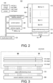
- the semiconductor memory device includes a memory array, a redundant information memory section, and a column selection control circuit.
- the memory array has a memory region including a plurality of memory cells and a redundant memory region including a plurality of memory cells.
- a column address of each column in the memory array corresponds to a set of an even column and an odd column.
- the redundant information memory section stores redundant information, wherein the redundant information includes an address of a bad column, identification information for identifying a failure in which one of the even column or the odd column of the bad column, and an address of a redundant column of the redundant memory region for repairing the bad column.
- the column selection control circuit selects a column of the memory array according to the column address.
- the semiconductor memory device further includes a page buffer, the page buffer keeps data read from the selected page of the memory array or keeps data programmed to the selected page, and the column selection control circuit selects data kept in the odd page or the even page in the page buffer.
- the redundant information includes addresses of a first bad column and a second bad column, when two column addresses of two adjacent columns are consistent with the addresses of the first bad column and the second bad column, one of the even column and the odd column of the first bad column having the failure is converted into the column of the redundant column based on the identification information, and the other one of the even column and the odd column of the first bad column without the failure is not converted into the another column of the redundant column, while one of the even column and the odd column of the second bad column not only having the failure but also adjacent to the column of the first bad column having the failure is converted into the another column of the redundant column.
- An embodiment of the invention provides a method for repairing a bad column of a semiconductor memory device including a memory array and a redundant information memory section.
- the memory array has a memory region including a plurality of memory cells and a redundant memory region including a plurality of memory cells.
- the method for repairing a bad column includes steps as follows: storing redundant information in the redundant information memory section, the redundant information comprises an address of a bad column including an even column and an odd column set as a set, an address of a redundant column in the redundant memory region for repairing the bad column, and identification information identifying a failure in which one of the even column or the odd column of the bad column; and selecting a column of the memory array.
- the step of selecting includes steps as follows: determining whether a column address of the column is consistent with the address of the bad column based on the redundant information; converting a column of the bad column having the failure into a column of the redundant column based on the identification information when the column address and the address of the bad column are consistent, and not converting another column of the bad column without the failure into another column of the redundant column.
- the step of selecting includes determining whether a failure exists in the even column or the odd column based on the identification information during a period of selecting an odd page or an even page.
- An embodiment of the invention provides a setting method for setting redundant information of a semiconductor memory device having a memory array.
- the memory array includes a memory region having a plurality of memory cells and a redundant memory region having a plurality of memory cells.
- the setting method includes steps as follows: detecting an address of a bad column; identifying a failure in one of an even column and an odd column of the bad column, and generating identification information according to a type or a combination of the failure; and setting the identification information and an address of a redundant column used to convert the detected bad column into a redundant column of the redundant memory region in the semiconductor memory device.
- the combination of the failure identifies a failure crossing the even column of a first bad column and the odd column of a second bad column or a failure crossing the odd column of the first bad column and the even column of the second bad column.
- the identification information identifying which one of the even column or the odd column of the bad column has a failure is stored as the redundant information, and the bad column is repaired by using the redundant column based on the identification information.
- unnecessary repair to the even column or the odd column that does not have a failure may be eliminated, so as to improve a repair efficiency of the redundant memory.
- the word line WL0 to the word line WL31, the source side selection line SGS and the drain side selection line SGD are connected to the word line selection circuit 160 through commonly input to a gate of a block selection transistor from a block selection line BSEL.
- the word line selection circuit 160 selects a block through the block selection line BSEL according to the row address information Ax. And based on an operation state, the word line selection circuit 160 suitably drives the source side selection line SGS, the drain side selection line SGD, and the word line WLO to the word line WL31 of the selected block.
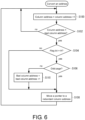
- the redundant information memory section 150 stores address information of a bad column (bad bit line) in the memory region MM or address information of a redundant column that repairs the bad column.
- a bad column is a physical defect in the product to be shipped.
- the bad column includes, for example, a defect such as a short circuit between adjacent columns, an open circuit in a column, or a defect of a memory unit.
- the redundant information includes an address of the bad column, a flag bit for identifying which of the even column or the odd column of the bad column has a failure, and an address of the redundant column for repairing the bad column.
- the redundant information is stored in a fuse ROM or other non-volatile media when the product is shipped, for example.
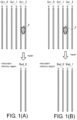
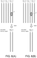
- the flag bit "L” indicates that the failure of the bad column starts from the even column
- the flag bit "H” indicates that the failure of the bad column starts from the odd bit.
- a column address Col_1 has the flag bit "H”, so the failure of the column address Col_1 is at the odd column
- a column address Col_2 has the flag bit "L”, so the failure of the column address Col_2 includes the even column.
- the failures of the column address Col_1 and the column address Col_2 demonstrate the situation of the bad columns of FIG. 1(B) .
- the column selection control circuit 180 determines whether any of column addresses that have increments from a starting column address is consistent with the address of the bad column. If consistent, the address pointer is moved to the column address of the redundant column.
- conversion of the column address differs according to a value of the flag bit that indicates a property of the bad column.
- the flag bit is "L"
- the bad column has a failure that starts from the even column, as shown in FIG.1 (A)
- a set of the even column and the odd column of the redundant column serves to repair a bad column including a set of even column and the odd column.
- the flag bit is "H"
- the control section 140 controls operations of respective parts of the flash memory based on the read command.
- the data kept by the page buffer/sense circuit 170 are continuously read.
- the column selection control circuit 180 makes the address of the starting column provided by the address register 130 increment, while reads the data kept in the page buffer/sense circuit 170 at the same time.
- the increment of the column address may be achieved by moving the address pointer by using software or using an address counter.
- the address of the bad column is converted into a column address of the redundant column (indicated as "R" in the figure) for an operation on the odd page.
- R column address of the redundant column
Landscapes
- For Increasing The Reliability Of Semiconductor Memories (AREA)
- Read Only Memory (AREA)
Claims (8)
- Dispositif de mémoire à semi-conducteur (100), comprenant :un réseau de mémoire (110), ayant une région de mémoire (MM) comprenant une pluralité de cellules de mémoire et une région de mémoire redondante (MR) comprenant une pluralité de cellules de mémoire, dans lequel une adresse de colonne de chaque ensemble de colonnes dans le réseau de mémoire (110) correspond à un ensemble d'une colonne paire (e) et d'une colonne impaire (o),dans lequel un circuit de détection est partagé par l'ensemble d'une colonne paire et d'une colonne impaire, et dans lequel une page paire est sélectionnée par la colonne paire et une page impaire est sélectionnée par la colonne impaire ;une section de mémoire d'informations redondantes (150), stockant des informations redondantes, dans lequel les informations redondantes comprennent une adresse de colonne erronée d'un ensemble de colonnes erronées (Col_1, Col_2), des informations d'identification permettant d'identifier une défaillance dans l'une parmi la colonne paire (e) ou la colonne impaire (o) de l'ensemble de colonnes erronées (Col_1, Col_2), et une adresse de colonne redondante d'un ensemble de colonnes redondantes (Red_0) de la région de mémoire redondante (MR) permettant de réparer l'ensemble de colonnes erronées (Col_1, Col_2) ; etun circuit de commande de sélection de colonne (180), configuré pour :sélectionner un ensemble de colonnes du réseau de mémoire (110) selon l'adresse de colonne,déterminer si l'adresse de colonne est cohérente avec l'adresse de colonne erronée de l'ensemble des colonnes erronées (Col_1, Col_2) en fonction des informations redondantes,déterminer si une défaillance existe dans une colonne impaire (o) ou une colonne paire (e) de l'ensemble de colonnes erronées (Col_1, Col_2) en fonction des informations d'identification lorsque l'adresse de colonne de l'ensemble de colonnes est cohérente avec l'adresse de colonne erronée de l'ensemble de colonnes erronées (Col_1, Col_2),dans lequel, lorsque la défaillance existe dans la colonne impaire (o) d'un premier ensemble de colonnes erronées (Col_1) et dans la colonne paire (e) d'un second ensemble de colonnes erronées (Col_2), dans lequel la colonne paire (e) du second ensemble de colonnes erronées (Col_2) est adjacente à la colonne impaire (o) du premier ensemble de colonnes erronées (Col_1) et la défaillance n'existe pas dans la colonne paire (e) du premier ensemble de colonnes erronées (Col_1) et la défaillance n'existe pas dans la colonne impaire (o) du second ensemble de colonnes erronées (Col_2), convertir la page paire (e) du second ensemble de colonnes erronées (Col_2) ayant la défaillance en une colonne de l'ensemble de colonnes redondantes (Red_0), et convertir la page impaire (o) du premier ensemble de colonnes erronées (Col_1) ayant la défaillance en une autre colonne de l'ensemble de colonnes redondantes (Red_0).
- Dispositif de mémoire à semi-conducteur (100) selon l'une quelconque des revendications 1 à 3, dans lequel, pendant une période pendant laquelle le circuit de commande de sélection de colonne (180) sélectionne la page impaire ou la page paire, le circuit de commande de sélection de colonne (180) détermine si une défaillance existe dans la colonne paire (e) ou la colonne impaire (o) en fonction des informations d'identification.
- Dispositif de mémoire à semi-conducteur (100) selon la revendication 2, dans lequel le dispositif de mémoire à semi-conducteur (100) comprend également un tampon de page (170), le tampon de page (170) conserve des données lues à partir de la page sélectionnée du réseau de mémoire (110) ou conserve des données programmées dans la page sélectionnée, et le circuit de commande de sélection de colonne (180) sélectionne des données conservées dans la page impaire ou la page paire dans le tampon de page (170).
- Dispositif de mémoire à semi-conducteur (100) selon la revendication 1, dans lequel les informations redondantes comprennent des adresses de colonnes erronées du premier ensemble de colonnes erronées (Col_1) et du second ensemble de colonnes erronées (Col_2), lorsque deux adresses de colonnes de deux colonnes adjacentes sont cohérentes avec les adresses du premier ensemble de colonnes erronées (Col_1) et du second ensemble de colonnes erronées (Col_2), l'une parmi la colonne paire (e) et la colonne impaire (o) du premier ensemble de colonnes erronées (Col_1) ayant la défaillance est convertie en la colonne de l'ensemble de colonnes redondantes (Red_0) en fonction des informations d'identification, et l'autre parmi la colonne paire (e) et la colonne impaire (o) du premier ensemble de colonnes erronées (Col_1) sans la défaillance n'est pas convertie en l'autre colonne de l'ensemble de colonnes redondantes (Red_0), tandis que l'une parmi la colonne paire (e) et la colonne impaire (o) du second ensemble de colonnes erronées (Col_2) non seulement ayant la défaillance, mais également adjacente à la colonne du premier ensemble de colonnes erronées ayant la défaillance est convertie en l'autre colonne de l'ensemble des colonnes redondantes (Red_0).
- Procédé de réparation d'une colonne erronée (Col_1, Col_2) d'un dispositif de mémoire à semi-conducteur (100), dans lequel le dispositif de mémoire à semi-conducteur (100) comprend un réseau de mémoire (110) et une section de mémoire d'informations redondantes (150), le réseau de mémoire (110) a une région de mémoire (MM) comprenant une pluralité de cellules de mémoire et une région de mémoire redondante (MR) comprenant une pluralité de cellules de mémoire, le procédé de réparation de la colonne erronée (Col_1, Col_2) comprenant les étapes suivantes :stockage d'informations redondantes dans la section de mémoire d'informations redondantes (150), les informations redondantes comprennent une adresse de colonne erronée d'un ensemble de colonnes erronées (Col_1, Col_2) comportant une colonne paire (e) et une colonne impaire (o) définies en tant qu'ensemble, une adresse de colonne redondante d'un ensemble de colonnes redondantes (Red_0) dans la région de mémoire redondante (MR) pour réparer l'ensemble de colonnes erronées (Col_1, Col_2) et des informations d'identification identifiant une défaillance dans l'une parmi la colonne paire (e) ou la colonne impaire (o) de l'ensemble de colonnes erronées (Col_1, Col_2) ; etsélection (S100) d'un ensemble de colonnes du réseau de mémoire (110), et détermination (S102) établissant si une adresse de colonne de la colonne est cohérente avec l'adresse de colonne erronée de l'ensemble de colonnes erronées (Col_1, Col_2) en fonction des informations redondantes ;détermination établissant si une défaillance existe dans une colonne impaire (o) ou une colonne paire (e) de l'ensemble de colonnes erronées (Col_1, Col_2) en fonction des informations d'identification lorsque l'adresse de colonne de l'ensemble de colonnes est cohérente avec l'adresse de colonne erronée de l'ensemble de colonnes erronées (Col_1, Col_2), dans lequel un circuit de détection est partagé par l'ensemble d'une colonne paire et d'une colonne impaire, et dans lequel une page paire est sélectionnée par la colonne paire et une page impaire est sélectionnée par la colonne impaire ;dans lequel, lorsque la défaillance existe dans la colonne impaire (o) d'un premier ensemble de colonnes erronées (Col_1) et dans la colonne paire (e) d'un ensemble de secondes colonnes erronées (Col_2), dans lequel la colonne paire (e) du second ensemble de colonnes erronées (Col_2) est adjacente à la colonne impaire (o) du premier ensemble de colonnes erronées (Col_1) et la défaillance n'existe pas dans la colonne paire (e) du premier ensemble de colonnes erronées (Col_1) et la défaillance n'existe pas dans la colonne impaire (o) du second ensemble de colonnes erronées (Col_2), conversion de la page paire (e) du second ensemble de colonnes erronées (Col_2) ayant la défaillance en une colonne de l'ensemble de colonnes redondantes (Red_0), et conversion de la page impaire (o) du premier ensemble de colonnes erronées (Col_1) ayant la défaillance en une autre colonne de l'ensemble de colonnes redondantes (Red_0).
- Procédé de réparation de la colonne erronée (Col_1, Col_2) selon la revendication 5, dans lequel les informations redondantes comportent des adresses de colonnes erronées du premier ensemble de colonnes erronées et du second ensemble de colonnes erronées, et l'étape de détermination comprenant la détermination établissant si deux adresses de colonne de deux colonnes adjacentes sont cohérentes avec les adresses du premier ensemble de colonnes erronées (Col_1) et du second ensemble de colonnes erronées (Col_2), et le procédé de réparation de la colonne erronée (Col_1, Col_2) comprend également la conversion d'une colonne du premier ensemble de colonnes erronées (Col_1) ayant la défaillance en une colonne de l'ensemble de colonnes redondantes (Red_0) en fonction des informations d'identification ; et l'absence de conversion de l'autre colonne du premier ensemble de colonnes erronées (Col_1) sans la défaillance en l'autre colonne de l'ensemble de colonnes redondantes (Red_0), mais la conversion d'une colonne de l'ensemble de secondes colonnes erronées (Col_2) non seulement ayant la défaillance mais également adjacente à la colonne du premier ensemble de colonnes erronées ayant la défaillance en l'autre colonne de l'ensemble de colonnes redondantes (Red_0).
- Procédé de définition pour la définition d'informations redondantes d'un dispositif de mémoire à semi-conducteur (100), dans lequel le dispositif de mémoire à semi-conducteur (100) comprend un réseau de mémoire (110), le réseau de mémoire (110) comprend une région de mémoire (MM) ayant une pluralité de cellules de mémoire et une région de mémoire redondante (MR) ayant une pluralité de cellules de mémoire, le procédé comprenant les étapes suivantes :détection (S200) d'une adresse de colonne erronée d'un ensemble de colonnes erronées (Col_1, Col_2) ;identification (S210) d'une défaillance dans l'une d'une colonne paire (e) et d'une colonne impaire (o) de l'ensemble de colonnes erronées (Col_1, Col_2) dans lequel un circuit de détection est partagé par l'ensemble d'une colonne paire et d'une colonne impaire, et dans lequel une page paire est sélectionnée par la colonne paire et une page impaire est sélectionnée par la colonne impaire ;et génération d'informations d'identification selon un type ou une combinaison de la défaillance ; etdéfinition (S220) des informations d'identification et d'une adresse de colonne redondante d'un ensemble de colonnes redondantes (Red_0) utilisées pour convertir l'ensemble détecté de colonnes erronées (Col_1, Col_2) en un ensemble de colonnes redondantes (Red_0) de la région de mémoire redondante (MR) dans le dispositif de mémoire à semi-conducteur (100), dans lequel les informations d'identification indiquent si la défaillance existe dans la colonne impaire (o) ou la colonne paire (e) de l'ensemble de colonnes erronées (Col_1, Col_2),lorsque la défaillance existe dans la colonne impaire (o) d'un premier ensemble de colonnes erronées (Col_1) et dans la colonne paire (e) d'un second ensemble de colonnes erronées (Col_2), dans lequel la colonne paire (e) du second ensemble de colonnes erronées (Col_2) est adjacente à la colonne impaire (o) du premier ensemble de colonnes erronées (Col_1) et la défaillance n'existe pas dans la colonne paire (e) du premier ensemble de colonnes erronées (Col_1) et la défaillance n'existe pas dans la colonne impaire (o) du second ensemble de colonnes erronées (Col_2), conversion de la page paire (e) du second ensemble de colonnes erronées (Col_2) en une colonne de l'ensemble de colonnes redondantes (Red_0), et conversion de la page impaire (o) du premier ensemble de colonnes erronées (Col_1) ayant la défaillance en une autre colonne de l'ensemble de colonnes redondantes (Red_0).
- Procédé de définition selon la revendication 7, dans lequel la combinaison de la défaillance identifie une défaillance croisant la colonne paire (e) du premier ensemble de colonnes erronées (Col_1) et la colonne impaire (o) du second ensemble de colonnes erronées (Col_2) ou une défaillance croisant la colonne impaire (o) du premier ensemble de colonnes erronées (Col_1) et la colonne paire (e) du second ensemble de colonnes erronées (Col_2).
Applications Claiming Priority (1)
| Application Number | Priority Date | Filing Date | Title |
|---|---|---|---|
| JP2015136735A JP6144729B2 (ja) | 2015-07-08 | 2015-07-08 | 半導体記憶装置 |
Publications (3)
| Publication Number | Publication Date |
|---|---|
| EP3115995A1 EP3115995A1 (fr) | 2017-01-11 |
| EP3115995C0 EP3115995C0 (fr) | 2025-04-09 |
| EP3115995B1 true EP3115995B1 (fr) | 2025-04-09 |
Family
ID=56615819
Family Applications (1)
| Application Number | Title | Priority Date | Filing Date |
|---|---|---|---|
| EP16178002.8A Active EP3115995B1 (fr) | 2015-07-08 | 2016-07-05 | Dispositif de mémoire à semi-conducteur, procédé de réparation de colonne défectueuse et procédé de réglage de ses informations redondantes |
Country Status (7)
| Country | Link |
|---|---|
| US (1) | US9627094B2 (fr) |
| EP (1) | EP3115995B1 (fr) |
| JP (1) | JP6144729B2 (fr) |
| KR (1) | KR101771635B1 (fr) |
| CN (1) | CN106340324B (fr) |
| ES (1) | ES3030458T3 (fr) |
| TW (1) | TWI595497B (fr) |
Families Citing this family (12)
| Publication number | Priority date | Publication date | Assignee | Title |
|---|---|---|---|---|
| KR101521258B1 (ko) * | 2013-09-10 | 2015-05-21 | 연세대학교 산학협력단 | 메모리 수리 방법 및 메모리 수리 장치 |
| US10002042B2 (en) * | 2015-10-22 | 2018-06-19 | Sandisk Technologies Llc | Systems and methods of detecting errors during read operations and skipping word line portions |
| KR102384864B1 (ko) * | 2017-11-03 | 2022-04-08 | 삼성전자주식회사 | 불량 스트링을 리페어하는 방법 및 불휘발성 메모리 장치 |
| US10971247B2 (en) * | 2018-03-29 | 2021-04-06 | Samsung Electronics Co., Ltd. | Semiconductor memory devices, memory systems, and methods of operating semiconductor memory devices |
| CN110867205B (zh) * | 2018-08-27 | 2021-10-08 | 华邦电子股份有限公司 | 存储器装置以及存储器周边电路 |
| US10908838B2 (en) | 2018-09-25 | 2021-02-02 | Sandisk Technologies Llc | Column replacement with non-dedicated replacement columns |
| US11373726B2 (en) | 2019-04-03 | 2022-06-28 | Texas Instruments Incorporated | Management of multiple memory in-field self-repair options |
| JP7238171B2 (ja) * | 2019-07-12 | 2023-03-13 | 長江存儲科技有限責任公司 | 不良カラム修復を提供するメモリデバイスおよびその動作方法 |
| KR102578438B1 (ko) * | 2020-10-20 | 2023-09-14 | 한양대학교 산학협력단 | 3차원 플래시 메모리에서의 수직 홀 불량 개선 방법 |
| US12374411B2 (en) | 2020-10-20 | 2025-07-29 | Samsung Electronics Co., Ltd. | Three-dimensional flash memory for improving integration and operation method thereof |
| TWI752704B (zh) * | 2020-11-03 | 2022-01-11 | 華邦電子股份有限公司 | 記憶體儲存裝置及其操作方法 |
| US11815995B1 (en) * | 2022-04-27 | 2023-11-14 | Macronix International Co., Ltd. | Redundancy schemes for repairing column defects |
Citations (1)
| Publication number | Priority date | Publication date | Assignee | Title |
|---|---|---|---|---|
| US20120057419A1 (en) * | 2010-09-06 | 2012-03-08 | Hynix Semiconductor Inc. | Semiconductor memory device and method of operating the same |
Family Cites Families (22)
| Publication number | Priority date | Publication date | Assignee | Title |
|---|---|---|---|---|
| JP2575919B2 (ja) * | 1990-03-22 | 1997-01-29 | 株式会社東芝 | 半導体記憶装置の冗長回路 |
| JP3568265B2 (ja) * | 1995-02-20 | 2004-09-22 | 富士通株式会社 | 半導体メモリ装置 |
| KR100268433B1 (ko) * | 1997-12-29 | 2000-10-16 | 윤종용 | 열 리던던시 구조를 가지는 반도체 메모리 장치 |
| US6199177B1 (en) * | 1998-08-28 | 2001-03-06 | Micron Technology, Inc. | Device and method for repairing a semiconductor memory |
| US6052318A (en) * | 1998-12-22 | 2000-04-18 | Siemens Aktiengesellschaft | Repairable semiconductor memory circuit having parrel redundancy replacement wherein redundancy elements replace failed elements |
| JP2000235800A (ja) | 1999-02-12 | 2000-08-29 | Mitsubishi Electric Corp | 半導体記憶装置 |
| JP2000311496A (ja) | 1999-04-28 | 2000-11-07 | Nec Corp | 冗長アドレス設定回路及びこれを内蔵した半導体記憶装置 |
| JP2002197888A (ja) * | 2000-12-26 | 2002-07-12 | Sanyo Electric Co Ltd | 半導体記憶装置 |
| JP2002208294A (ja) * | 2001-01-12 | 2002-07-26 | Toshiba Corp | リダンダンシーシステムを有する半導体記憶装置 |
| KR100385956B1 (ko) * | 2001-02-14 | 2003-06-02 | 삼성전자주식회사 | 효율적인 칼럼 리던던시 스킴을 갖는 반도체 메모리장치 |
| JP2002288993A (ja) | 2001-03-23 | 2002-10-04 | Mitsubishi Electric Corp | 半導体記憶装置 |
| TW594775B (en) * | 2001-06-04 | 2004-06-21 | Toshiba Corp | Semiconductor memory device |
| US6704228B2 (en) | 2001-12-28 | 2004-03-09 | Samsung Electronics Co., Ltd | Semiconductor memory device post-repair circuit and method |
| KR100563736B1 (ko) | 2004-01-16 | 2006-03-28 | 주식회사 하이닉스반도체 | 반도체 메모리 소자의 리페어 장치 |
| WO2005081260A1 (fr) * | 2004-02-20 | 2005-09-01 | Spansion Llc | Dispositif de stockage a semiconducteur et procede de redondance pour un dispositif de stockage a semiconducteur |
| US7286380B2 (en) * | 2005-09-29 | 2007-10-23 | Intel Corporation | Reconfigurable memory block redundancy to repair defective input/output lines |
| US7949908B2 (en) * | 2006-10-11 | 2011-05-24 | Marvell Israel (M.I.S.L) Ltd. | Memory repair system and method |
| US7996736B2 (en) * | 2008-10-26 | 2011-08-09 | Sandisk 3D Llc | Bad page marking strategy for fast readout in memory |
| US20120075943A1 (en) * | 2010-09-29 | 2012-03-29 | Macronix International Co., Ltd. | Method and Apparatus for Memory Repair With Redundant Columns |
| KR101196907B1 (ko) * | 2010-10-27 | 2012-11-05 | 에스케이하이닉스 주식회사 | 반도체 메모리 장치 및 그의 동작 방법 |
| JP5378574B1 (ja) * | 2012-06-13 | 2013-12-25 | ウィンボンド エレクトロニクス コーポレーション | 半導体記憶装置 |
| JP2014186772A (ja) | 2013-03-22 | 2014-10-02 | Toshiba Corp | 半導体記憶装置、コントローラ、及びメモリシステム |
-
2015
- 2015-07-08 JP JP2015136735A patent/JP6144729B2/ja active Active
-
2016
- 2016-06-16 TW TW105118913A patent/TWI595497B/zh active
- 2016-07-05 ES ES16178002T patent/ES3030458T3/es active Active
- 2016-07-05 EP EP16178002.8A patent/EP3115995B1/fr active Active
- 2016-07-06 US US15/202,578 patent/US9627094B2/en active Active
- 2016-07-06 CN CN201610527692.4A patent/CN106340324B/zh active Active
- 2016-07-06 KR KR1020160085769A patent/KR101771635B1/ko active Active
Patent Citations (1)
| Publication number | Priority date | Publication date | Assignee | Title |
|---|---|---|---|---|
| US20120057419A1 (en) * | 2010-09-06 | 2012-03-08 | Hynix Semiconductor Inc. | Semiconductor memory device and method of operating the same |
Also Published As
| Publication number | Publication date |
|---|---|
| EP3115995C0 (fr) | 2025-04-09 |
| US20170011809A1 (en) | 2017-01-12 |
| KR20170007154A (ko) | 2017-01-18 |
| JP6144729B2 (ja) | 2017-06-07 |
| CN106340324A (zh) | 2017-01-18 |
| TWI595497B (zh) | 2017-08-11 |
| KR101771635B1 (ko) | 2017-08-25 |
| CN106340324B (zh) | 2020-01-21 |
| ES3030458T3 (en) | 2025-06-30 |
| EP3115995A1 (fr) | 2017-01-11 |
| JP2017021872A (ja) | 2017-01-26 |
| TW201715533A (zh) | 2017-05-01 |
| US9627094B2 (en) | 2017-04-18 |
Similar Documents
| Publication | Publication Date | Title |
|---|---|---|
| EP3115995B1 (fr) | Dispositif de mémoire à semi-conducteur, procédé de réparation de colonne défectueuse et procédé de réglage de ses informations redondantes | |
| CN103489486B (zh) | 存储器装置以及冗余方法 | |
| US7525839B2 (en) | Semiconductor memory device capable of correcting a read level properly | |
| US20120257453A1 (en) | Nonvolatile semiconductor memory device | |
| KR101950758B1 (ko) | 반도체 장치 | |
| US8194465B2 (en) | Non-volatile semiconductor storage device | |
| US8605514B2 (en) | Nonvolatile semiconductor memory device | |
| KR101731576B1 (ko) | 반도체 기억장치 및 nand 플래시 메모리의 프로그램 방법 | |
| US10395753B2 (en) | Semiconductor memory device and programming method thereof | |
| KR101699476B1 (ko) | 반도체 기억장치 | |
| US20150121174A1 (en) | Semiconductor storing device and redundancy method thereof | |
| JP5336053B2 (ja) | 不揮発性メモリ装置及びその動作方法 | |
| US10803954B2 (en) | Memory system | |
| US20120063237A1 (en) | Nonvolatile memory device and method of operating the same | |
| US7558118B2 (en) | NAND flash memory device | |
| CN105321566A (zh) | 半导体存储装置及其编程方法 | |
| JP2010108548A (ja) | 不揮発性半導体記憶装置とその制御方法 | |
| KR101651573B1 (ko) | 반도체 기억장치 및 그 프로그래밍 방법 | |
| TWI478170B (zh) | 記憶體裝置以及冗餘方法 | |
| TWI521530B (zh) | 半導體記憶裝置及其編程方法 | |
| JP5710815B1 (ja) | 半導体記憶装置 |
Legal Events
| Date | Code | Title | Description |
|---|---|---|---|
| PUAI | Public reference made under article 153(3) epc to a published international application that has entered the european phase |
Free format text: ORIGINAL CODE: 0009012 |
|
| STAA | Information on the status of an ep patent application or granted ep patent |
Free format text: STATUS: REQUEST FOR EXAMINATION WAS MADE |
|
| 17P | Request for examination filed |
Effective date: 20160705 |
|
| AK | Designated contracting states |
Kind code of ref document: A1 Designated state(s): AL AT BE BG CH CY CZ DE DK EE ES FI FR GB GR HR HU IE IS IT LI LT LU LV MC MK MT NL NO PL PT RO RS SE SI SK SM TR |
|
| AX | Request for extension of the european patent |
Extension state: BA ME |
|
| STAA | Information on the status of an ep patent application or granted ep patent |
Free format text: STATUS: EXAMINATION IS IN PROGRESS |
|
| 17Q | First examination report despatched |
Effective date: 20200701 |
|
| GRAP | Despatch of communication of intention to grant a patent |
Free format text: ORIGINAL CODE: EPIDOSNIGR1 |
|
| STAA | Information on the status of an ep patent application or granted ep patent |
Free format text: STATUS: GRANT OF PATENT IS INTENDED |
|
| INTG | Intention to grant announced |
Effective date: 20241119 |
|
| GRAS | Grant fee paid |
Free format text: ORIGINAL CODE: EPIDOSNIGR3 |
|
| GRAA | (expected) grant |
Free format text: ORIGINAL CODE: 0009210 |
|
| STAA | Information on the status of an ep patent application or granted ep patent |
Free format text: STATUS: THE PATENT HAS BEEN GRANTED |
|
| AK | Designated contracting states |
Kind code of ref document: B1 Designated state(s): AL AT BE BG CH CY CZ DE DK EE ES FI FR GB GR HR HU IE IS IT LI LT LU LV MC MK MT NL NO PL PT RO RS SE SI SK SM TR |
|
| REG | Reference to a national code |
Ref country code: GB Ref legal event code: FG4D |
|
| REG | Reference to a national code |
Ref country code: CH Ref legal event code: EP |
|
| REG | Reference to a national code |
Ref country code: IE Ref legal event code: FG4D |
|
| U01 | Request for unitary effect filed |
Effective date: 20250409 |
|
| U07 | Unitary effect registered |
Designated state(s): AT BE BG DE DK EE FI FR IT LT LU LV MT NL PT RO SE SI Effective date: 20250415 |
|
| REG | Reference to a national code |
Ref country code: ES Ref legal event code: FG2A Ref document number: 3030458 Country of ref document: ES Kind code of ref document: T3 Effective date: 20250630 |
|
| U20 | Renewal fee for the european patent with unitary effect paid |
Year of fee payment: 10 Effective date: 20250725 |
|
| PGFP | Annual fee paid to national office [announced via postgrant information from national office to epo] |
Ref country code: ES Payment date: 20250812 Year of fee payment: 10 |
|
| PG25 | Lapsed in a contracting state [announced via postgrant information from national office to epo] |
Ref country code: NO Free format text: LAPSE BECAUSE OF FAILURE TO SUBMIT A TRANSLATION OF THE DESCRIPTION OR TO PAY THE FEE WITHIN THE PRESCRIBED TIME-LIMIT Effective date: 20250709 Ref country code: GR Free format text: LAPSE BECAUSE OF FAILURE TO SUBMIT A TRANSLATION OF THE DESCRIPTION OR TO PAY THE FEE WITHIN THE PRESCRIBED TIME-LIMIT Effective date: 20250710 |
|
| PG25 | Lapsed in a contracting state [announced via postgrant information from national office to epo] |
Ref country code: PL Free format text: LAPSE BECAUSE OF FAILURE TO SUBMIT A TRANSLATION OF THE DESCRIPTION OR TO PAY THE FEE WITHIN THE PRESCRIBED TIME-LIMIT Effective date: 20250409 |
|
| PGFP | Annual fee paid to national office [announced via postgrant information from national office to epo] |
Ref country code: GB Payment date: 20250722 Year of fee payment: 10 |
|
| PG25 | Lapsed in a contracting state [announced via postgrant information from national office to epo] |
Ref country code: HR Free format text: LAPSE BECAUSE OF FAILURE TO SUBMIT A TRANSLATION OF THE DESCRIPTION OR TO PAY THE FEE WITHIN THE PRESCRIBED TIME-LIMIT Effective date: 20250409 |
|
| PG25 | Lapsed in a contracting state [announced via postgrant information from national office to epo] |
Ref country code: RS Free format text: LAPSE BECAUSE OF FAILURE TO SUBMIT A TRANSLATION OF THE DESCRIPTION OR TO PAY THE FEE WITHIN THE PRESCRIBED TIME-LIMIT Effective date: 20250709 |
|
| PG25 | Lapsed in a contracting state [announced via postgrant information from national office to epo] |
Ref country code: IS Free format text: LAPSE BECAUSE OF FAILURE TO SUBMIT A TRANSLATION OF THE DESCRIPTION OR TO PAY THE FEE WITHIN THE PRESCRIBED TIME-LIMIT Effective date: 20250809 |
|
| PG25 | Lapsed in a contracting state [announced via postgrant information from national office to epo] |
Ref country code: SM Free format text: LAPSE BECAUSE OF FAILURE TO SUBMIT A TRANSLATION OF THE DESCRIPTION OR TO PAY THE FEE WITHIN THE PRESCRIBED TIME-LIMIT Effective date: 20250409 |
|
| PG25 | Lapsed in a contracting state [announced via postgrant information from national office to epo] |
Ref country code: CZ Free format text: LAPSE BECAUSE OF FAILURE TO SUBMIT A TRANSLATION OF THE DESCRIPTION OR TO PAY THE FEE WITHIN THE PRESCRIBED TIME-LIMIT Effective date: 20250409 |
|
| PG25 | Lapsed in a contracting state [announced via postgrant information from national office to epo] |
Ref country code: SK Free format text: LAPSE BECAUSE OF FAILURE TO SUBMIT A TRANSLATION OF THE DESCRIPTION OR TO PAY THE FEE WITHIN THE PRESCRIBED TIME-LIMIT Effective date: 20250409 |
|
| PLBE | No opposition filed within time limit |
Free format text: ORIGINAL CODE: 0009261 |
|
| STAA | Information on the status of an ep patent application or granted ep patent |
Free format text: STATUS: NO OPPOSITION FILED WITHIN TIME LIMIT |
|
| REG | Reference to a national code |
Ref country code: CH Ref legal event code: L10 Free format text: ST27 STATUS EVENT CODE: U-0-0-L10-L00 (AS PROVIDED BY THE NATIONAL OFFICE) Effective date: 20260218 |
|
| REG | Reference to a national code |
Ref country code: CH Ref legal event code: H13 Free format text: ST27 STATUS EVENT CODE: U-0-0-H10-H13 (AS PROVIDED BY THE NATIONAL OFFICE) Effective date: 20260224 |
|
| 26N | No opposition filed |
Effective date: 20260112 |
|
| PG25 | Lapsed in a contracting state [announced via postgrant information from national office to epo] |
Ref country code: CH Free format text: LAPSE BECAUSE OF NON-PAYMENT OF DUE FEES Effective date: 20250731 |