EP3109908A2 - Lichtemittierende vorrichtung und herstellungsverfahren dafür - Google Patents
Lichtemittierende vorrichtung und herstellungsverfahren dafür Download PDFInfo
- Publication number
- EP3109908A2 EP3109908A2 EP16176228.1A EP16176228A EP3109908A2 EP 3109908 A2 EP3109908 A2 EP 3109908A2 EP 16176228 A EP16176228 A EP 16176228A EP 3109908 A2 EP3109908 A2 EP 3109908A2
- Authority
- EP
- European Patent Office
- Prior art keywords
- fluorescent
- light emitting
- resin
- emitting device
- layer
- Prior art date
- Legal status (The legal status is an assumption and is not a legal conclusion. Google has not performed a legal analysis and makes no representation as to the accuracy of the status listed.)
- Withdrawn
Links
Images


Classifications
-
- H—ELECTRICITY
- H10—SEMICONDUCTOR DEVICES; ELECTRIC SOLID-STATE DEVICES NOT OTHERWISE PROVIDED FOR
- H10H—INORGANIC LIGHT-EMITTING SEMICONDUCTOR DEVICES HAVING POTENTIAL BARRIERS
- H10H20/00—Individual inorganic light-emitting semiconductor devices having potential barriers, e.g. light-emitting diodes [LED]
- H10H20/80—Constructional details
- H10H20/85—Packages
- H10H20/851—Wavelength conversion means
- H10H20/8511—Wavelength conversion means characterised by their material, e.g. binder
- H10H20/8512—Wavelength conversion materials
- H10H20/8513—Wavelength conversion materials having two or more wavelength conversion materials
-
- H—ELECTRICITY
- H10—SEMICONDUCTOR DEVICES; ELECTRIC SOLID-STATE DEVICES NOT OTHERWISE PROVIDED FOR
- H10H—INORGANIC LIGHT-EMITTING SEMICONDUCTOR DEVICES HAVING POTENTIAL BARRIERS
- H10H20/00—Individual inorganic light-emitting semiconductor devices having potential barriers, e.g. light-emitting diodes [LED]
- H10H20/01—Manufacture or treatment
- H10H20/034—Manufacture or treatment of coatings
-
- H—ELECTRICITY
- H10—SEMICONDUCTOR DEVICES; ELECTRIC SOLID-STATE DEVICES NOT OTHERWISE PROVIDED FOR
- H10H—INORGANIC LIGHT-EMITTING SEMICONDUCTOR DEVICES HAVING POTENTIAL BARRIERS
- H10H20/00—Individual inorganic light-emitting semiconductor devices having potential barriers, e.g. light-emitting diodes [LED]
- H10H20/01—Manufacture or treatment
- H10H20/036—Manufacture or treatment of packages
- H10H20/0361—Manufacture or treatment of packages of wavelength conversion means
-
- H—ELECTRICITY
- H10—SEMICONDUCTOR DEVICES; ELECTRIC SOLID-STATE DEVICES NOT OTHERWISE PROVIDED FOR
- H10H—INORGANIC LIGHT-EMITTING SEMICONDUCTOR DEVICES HAVING POTENTIAL BARRIERS
- H10H20/00—Individual inorganic light-emitting semiconductor devices having potential barriers, e.g. light-emitting diodes [LED]
- H10H20/80—Constructional details
- H10H20/81—Bodies
- H10H20/822—Materials of the light-emitting regions
- H10H20/824—Materials of the light-emitting regions comprising only Group III-V materials, e.g. GaP
- H10H20/825—Materials of the light-emitting regions comprising only Group III-V materials, e.g. GaP containing nitrogen, e.g. GaN
-
- H—ELECTRICITY
- H10—SEMICONDUCTOR DEVICES; ELECTRIC SOLID-STATE DEVICES NOT OTHERWISE PROVIDED FOR
- H10H—INORGANIC LIGHT-EMITTING SEMICONDUCTOR DEVICES HAVING POTENTIAL BARRIERS
- H10H20/00—Individual inorganic light-emitting semiconductor devices having potential barriers, e.g. light-emitting diodes [LED]
- H10H20/80—Constructional details
- H10H20/83—Electrodes
- H10H20/831—Electrodes characterised by their shape
-
- H—ELECTRICITY
- H10—SEMICONDUCTOR DEVICES; ELECTRIC SOLID-STATE DEVICES NOT OTHERWISE PROVIDED FOR
- H10H—INORGANIC LIGHT-EMITTING SEMICONDUCTOR DEVICES HAVING POTENTIAL BARRIERS
- H10H20/00—Individual inorganic light-emitting semiconductor devices having potential barriers, e.g. light-emitting diodes [LED]
- H10H20/80—Constructional details
- H10H20/84—Coatings, e.g. passivation layers or antireflective coatings
-
- H—ELECTRICITY
- H10—SEMICONDUCTOR DEVICES; ELECTRIC SOLID-STATE DEVICES NOT OTHERWISE PROVIDED FOR
- H10H—INORGANIC LIGHT-EMITTING SEMICONDUCTOR DEVICES HAVING POTENTIAL BARRIERS
- H10H20/00—Individual inorganic light-emitting semiconductor devices having potential barriers, e.g. light-emitting diodes [LED]
- H10H20/80—Constructional details
- H10H20/85—Packages
- H10H20/851—Wavelength conversion means
- H10H20/8514—Wavelength conversion means characterised by their shape, e.g. plate or foil
-
- H—ELECTRICITY
- H10—SEMICONDUCTOR DEVICES; ELECTRIC SOLID-STATE DEVICES NOT OTHERWISE PROVIDED FOR
- H10H—INORGANIC LIGHT-EMITTING SEMICONDUCTOR DEVICES HAVING POTENTIAL BARRIERS
- H10H20/00—Individual inorganic light-emitting semiconductor devices having potential barriers, e.g. light-emitting diodes [LED]
- H10H20/80—Constructional details
- H10H20/85—Packages
- H10H20/852—Encapsulations
- H10H20/854—Encapsulations characterised by their material, e.g. epoxy or silicone resins
-
- H—ELECTRICITY
- H10—SEMICONDUCTOR DEVICES; ELECTRIC SOLID-STATE DEVICES NOT OTHERWISE PROVIDED FOR
- H10H—INORGANIC LIGHT-EMITTING SEMICONDUCTOR DEVICES HAVING POTENTIAL BARRIERS
- H10H20/00—Individual inorganic light-emitting semiconductor devices having potential barriers, e.g. light-emitting diodes [LED]
- H10H20/80—Constructional details
- H10H20/85—Packages
- H10H20/855—Optical field-shaping means, e.g. lenses
- H10H20/856—Reflecting means
-
- H—ELECTRICITY
- H10—SEMICONDUCTOR DEVICES; ELECTRIC SOLID-STATE DEVICES NOT OTHERWISE PROVIDED FOR
- H10H—INORGANIC LIGHT-EMITTING SEMICONDUCTOR DEVICES HAVING POTENTIAL BARRIERS
- H10H20/00—Individual inorganic light-emitting semiconductor devices having potential barriers, e.g. light-emitting diodes [LED]
- H10H20/80—Constructional details
- H10H20/85—Packages
- H10H20/857—Interconnections, e.g. lead-frames, bond wires or solder balls
-
- H—ELECTRICITY
- H10—SEMICONDUCTOR DEVICES; ELECTRIC SOLID-STATE DEVICES NOT OTHERWISE PROVIDED FOR
- H10H—INORGANIC LIGHT-EMITTING SEMICONDUCTOR DEVICES HAVING POTENTIAL BARRIERS
- H10H20/00—Individual inorganic light-emitting semiconductor devices having potential barriers, e.g. light-emitting diodes [LED]
- H10H20/01—Manufacture or treatment
- H10H20/036—Manufacture or treatment of packages
-
- H10W72/01515—
-
- H10W72/075—
-
- H10W74/00—
-
- H10W90/726—
Definitions
- the present invention relates to a light emitting device having an LED chip.
- a fluorescent material is generally disposed on LED chip by means of dispensing, molding, spray coating and so on.
- these conventional methods have problems concerning process control and costs due to their processing properties.
- dispensing tends to see precipitation of the fluorescent material that in turn brings about the yellow-halo problem, leading to inconsistent color temperature and a wide range of bins.
- Molding has distribution of the fluorescent material vary with distribution of pressure, and also tends to have inconsistent color temperature and a wide range of bins.
- Spray coating is less subject to problems related to inconsistent color temperature and a wide range of bins, but the process requires repeated spray coating and tests, making it a time-consuming and low-material-utilization approach.
- anisotropic conductive adhesive is also used in the industry for binding before molding is performed to install a translucent layer.
- ACA anisotropic conductive adhesive
- FIG. 1 electrodes 208a, 208b of the chip 206 are bound to electrode pads 202a, 202b in the substrate 200 by means of anisotropic conductive adhesive (ACA) 204.
- ACA anisotropic conductive adhesive
- a light emitting device of the present invention comprises: a substrate; an LED chip, disposed on the substrate; and a fluorescent layer, the fluorescent layer being at least partially and conformally coated on the LED chip and the substrate.
- the light emitting device further comprises a reflective portion, surrounding the LED chip and/or the fluorescent layer.
- the light emitting device comprises a translucent layer coated on the fluorescent layer.
- the present invention uses semi-cured fluorescent resin to form the fluorescent layer, and this approach has at least the following advantages:
- the disclosed packaging scheme is suitable for various LED devices from and processes for all types of chips, making it of great industrial applicability.
- the disclosed packaging method conformally disposes the fluorescent layer on the LED chip.
- the encapsulation resin suitable has its moisture permeability below 11 g/m 2 /24Hr and has its oxygen permeability below 400 cm 3 /m 2 /24Hr so as to reduce impact of moisture/oxygen on the fluorescent material.
- the encapsulation resin with specific physical properties, reliability of the fluorescent material can be effectively improved.
- tetravalent-manganese-activated red fluorescent material is subject to hydrolysis when affected by moisture and has its luminous efficacy and reliability degraded.
- the red fluorescent material has a chemical formula of A 2 [MF 6 ]:Mn 4+ , wherein A is selected from Li, Na, K, Rb, Cs, NH 4 and any combination thereof and M is selected from Ge, Si, Sn, Ti, Zr and any combination thereof.
- fluorescent materials of other color may be used for further expanding the color gamut of the resultant light emitting device.
- the encapsulation resin refers to any resin covering the LED chip for packaging the chip.
- it may solely refer to a fluorescent layer (where there is no translucent layer), or a combination of a fluorescent layer and a translucent layer (where there is a translucent layer).
- dispensing resin In a dispensing process, it may refer to dispensing resin. Such dispensing process will be described in detail later.
- FIG. 3 shows a light emitting device 30 of the present invention, which comprises a substrate 300, an LED chip 302 disposed on substrate 300, and a fluorescent layer 304.
- the fluorescent layer 304 is at least partially and conformally coated on LED chip 302 and the substrate 300. While some details of the LED chip such as electrodes, substrate electrodes and die bonding material are omitted from FIG. 3 , people skilled in the art would understand, by referring to the present invention, that these details are not intended to be limited in the present invention and various embodiments of these components shall be within the scope of the present invention.
- the fluorescent layer 304 contains fluorescent material at a concentration that the fluorescent material is distributed evenly across the fluorescent layer 304, so as to prevent inconsistent color temperature. However, distribution of the fluorescent material may be alternatively distributed in an uneven way, such as in a gradient, according to the practical needs.
- a carrier forms substrates after cutting.
- the substrate/carrier may be a board made of any suitable material, such as a metal leadframe, a printed circuit board, a ceramic board, a glass board, a plastic board and a flexible board.
- the metal leadframe has its internal space filled with a space filler, so as to enhance the overall mechanical strength of the leadframe.
- the carrier may be removed after a later singulation step, so as to produce a light emitting device without substrate.
- the carrier is preferably one with release film on it, so it can be easily removed from the light emitting device when the final singulation step has been done.
- any suitable LED chip may be used.
- the LED chip may be one made of any GaN-based semiconductors, e.g. an InGaN chip. More preferably, the LED chip has a peak wavelength between 450 nm and 460 nm.
- the LED chip may be one of any of various designs, e.g. a horizontal chip, a vertical chip and a flip chip. It is to be specially noted that both horizontal and vertical chips require a conductive wire for connection with external electrodes. Such conductive wire and other components as well as their assembly will be detailed by means of some embodiments provided later.
- the fluorescent material may be one or more selected from the group consisting of: Sr 5 (PO 4 );Cl:Eu 2+ , (Sr,Ba)MgAl 10 O 17 :Eu 2+ , (Sr,Ba) 3 MgSi 2 O 8 :Eu 2+ , SrAl 2 O 4 :Eu 2+ , SrBaSiO 4 :Eu 2+ , CdS:In, CaS:Ce 3+ , Y 3 (Al,Gd) 5 O 12 :Ce 2+ , Ca 3 Sc 2 Si 3 O 12 :Ce 3+ , SrSiON:Eu 2+ , ZnS:Al 3+ ,Cu + , CaS:Sn 2+ , CaS:Sn 2+ ,F, CaSO 4 :Ce 3+ ,Mn 2+ , LiAlO 2 :M
- red fluorescent material activated by tetravalent manganese may be used in the present invention.
- red fluorescent material has a chemical formula of:
- A is selected from Li, Na, K, Rb, Cs, NH 4 and any combination thereof and M is selected from Ge, Si, Sn, Ti, Zr and any combination thereof.
- the red fluorescent material has an average particle size (d50) preferably between 18 ⁇ m and 41 ⁇ m.
- red fluorescent material examples include: K 2 SiF 6 :Mn 4+ , K 2 TiF 6 :Mn 4+ and K 2 GeF 6 :Mn 4+ in which K 2 SiF 6 :Mn 4+ is preferable.
- These red fluorescent materials when excited by a light source having a peak in a wavelength range between 450nm and 460nm can emit light having a primary peak in a wavelength range between 600nm and 650nm. It is to be noted that the primary peak mentioned herein refers to the wavelength at which point the fluorescent materials reach the greatest luminous intensity thereof.
- the present invention is not limited to use of a single red fluorescent material, and two or more fluorescent materials recited previously can be used together.
- an oxynitride fluorescent material as a green light source. More preferably, the green fluorescent material has a chemical formula selected from the group consisting of:
- the red fluorescent material and the green fluorescent material have a weight ratio of 1:1 ⁇ 3:1 because such ratio endows the resultant light emitting device with better color rendering.
- the fluorescent layer is formed by curing and cutting semi-cured fluorescent resin.
- the semi-cured fluorescent resin referred to herein is a B-stage resin composition. Under this state, the resin composition has good shape-retaining ability, yet is capable of deforming under external force, and it softens when heated and swells when contacting a solvent, without being fully melted or dissolved.
- the semi-cured fluorescent resin comprises a fluorescent material, a siloxane resin, a catalyst and a solvent. Based on the weight of the fluorescent layer, the weight of the fluorescent material is 10% to 60%; the weight of the siloxane resin is 28% to 89.3%; the weight of the catalyst is 0.1% to 2%; and the weight of the solvent is 0.1% to 2%.
- the semi-cured fluorescent resin may also comprise a softening agent.
- the weight of the softening agent is 0.5% to 8%.
- the solvent evaporates therefrom.
- the weight of the fluorescent material is 10% to 61.2%; the weight of the siloxane resin is 28% to 91.1%; and the weight of the catalyst is 0.1% to 2%.
- the weight of the softening agent is 0.5% to 8.2%.
- the fluorescent layer may be made of resin having its moisture permeability below 11 g/m 2 /24Hr and having its oxygen permeability below 400 cm 3 /m 2 /24Hr.
- the resin us such selected that its moisture permeability is below 10.5 g/m 2 /24Hr, and oxygen permeability is below 382 cm 3 /m 2 /24Hr, so as to reduce hydrolysis or degradation of the fluorescent material and in turn improve the overall reliability of the light emitting device.
- Such selection of the resin improves the reliability of the tetravalent-manganese-activated red fluorescent material significantly.
- moisture permeability refers to measured values obtained using TSY-TH1 Water Vapor Permeability Tester
- oxygen permeability refers to measured values obtained using i-Oxtra 7600 Oxygen Permeation Analyzer.
- the present invention may further comprise a reflective portion.
- the reflective portion is formed by curing and cutting reflective resin.
- the reflective resin is a resin composition containing reflective particles.
- the reflective particles contribute to high light convergence and may be selected form TiO 2 , SiO 2 , ZrO, MgO, BaSO 4 and any combination thereof, in which TiO 2 is preferable.
- the resin may be epoxide-based resin or siloxane-based resin, in which siloxane-based resin is preferable.
- the translucent layer is made by curing and cutting translucent resin and may comprise light-diffusing particles for further enhanced uniformity of light.
- the light-diffusing particles may be selected from BN, SiO 2 and the combination thereof.
- the translucent layer and the semi-cured fluorescent resin have the same basic resin and are formed into translucent layers through similar processes, with the only difference relying on addition of the fluorescent material.
- the translucent layer is also conformal, and the cured translucent layer serves to protect the fluorescent layer by preventing moisture from entering the fluorescent layer, so as to improve endurance of the light emitting device.
- the translucent layer has its moisture permeability and oxygen permeability preferably lower than those of the fluorescent layer, making it more protective.
- the translucent layer is made of resin having its moisture permeability below 11 g/m 2 /24Hr and having its oxygen permeability below 400 cm 3 /m 2 /24Hr.
- the resin has its moisture permeability below 10.5 g/m 2 /24Hr, and has its oxygen permeability below 382 cm 3 /m 2 /24Hr.
- a first embodiment is herein described in detail to illustrate the fluorescent layer of the present invention in regards of process and characteristic.
- a siloxane resin, a fluorescent material, a catalyst, a solvent and optionally a softening agent are mixed to form a mixture with the contents of the components as defined previously.
- the solvent may be any organic solvent that can be melting blended/mixed with the foregoing materials, preferably toluene.
- the fluorescent material is selected as described above.
- the present invention has no limitation to the method of mixing, as long as the practice makes the fluorescent material, the catalyst, the solvent and the optional softening agent well mixed. In the embodiments mentioned below, a vacuum deaearation mixer is used as an example.
- the present invention has no limitation to the method of applying, and the method may be rotary coating, spin coating, knife coating, and dipping coating.
- the thin layer is such made that its thickness is 50 ⁇ m to 250 ⁇ m, more preferably 70 ⁇ m to 185 ⁇ m.
- knife coating is used for forming the thin layer as an example.
- the thickness is below 45 ⁇ m, the fluorescent resin tends to have weakened strength, and the fluorescent material tends to have uneven distribution and in turn poor color uniformity.
- a thickness greater than 250 ⁇ m is too thick and thus leads to unnecessary high material costs. Besides, the excessive thickness thickens the final light emitting device, and is against the prevailing trend toward microminiaturization.
- the thin layer After being formed, the thin layer is processed into a semi-cured state.
- the method for making the thin layer a semi-cured one may be any suitable technologies without limitation, and preferably baking.
- the baking temperature is preferably performed for 1 to 4 hours at 65°C to 75°C so as to endow the fluorescent layer with acceptable shape-retaining ability and ability to deform under external force.
- the thin layer may be put aside for a while or performs centrifugal treatment to let the fluorescent material deposit at the bottom of the thin layer.
- thin layers each having different concentrations of the fluorescent material or having different types of fluorescent materials may be stacked and baked together, so as to form a laminated semi-cured fluorescent layer.
- the semi-cured thin layer is cut into pieces of semi-cured fluorescent resin.
- the cutting may be performed in any manner without limitation.
- the present invention may include measuring color temperature of the cut pieces of semi-cured fluorescent resin, so as to sort the cut pieces by color temperature.
- the thin layer was baked for 2 hours in an oven of 70°C, so that the resin was partially cured and became B-stage/semi-cured fluorescent resin.
- the semi-cured fluorescent resin was at last cut into a predetermined size.
- a blue light emitting diode having a wavelength of 460 nm was used for measuring color temperature so as to sort the cut pieces of the semi-cured fluorescent resin by color temperature.
- the semi-cured fluorescent resin can be used to make the disclosed light emitting device.
- the process for making the light emitting device of the present invention is herein explained with reference to the accompanying drawings.
- a carrier 500 is provided.
- the carrier 500 is selected as described previously.
- the light emitting device has a substrate, there is an electrically conductive pattern (not shown) in the substrate in addition to the metal leadframe.
- the electrically conductive pattern allows the LED chip 502 after packaged to have electrical connection with an external circuit.
- the carrier 500 of FIG. 5A may be any carrying body, and preferably one provided with release film. The release film facilitates removal of the carrier from the light emitting device after the last step, namely singulation. Afterward, the LED chip 502 is deposited on the carrier 500.
- the LED chip 502 may be permanently fixed to the carrier 500 using solder, die bond paste or similar materials. Where there is no substrate, the chip 502 can be temporarily fixed to the carrier 500 via release film or other less adhesive materials. In addition, where the LED chip 502 is a vertical chip or a horizontal chip, a conductive wire has to be connected to the electric pattern of the carrier 500, and this will be discussed later with a particular embodiment.
- semi-cured fluorescent resin 504 as made in the first embodiment is deposited to the carrier 500 having the LED chip 502, as shown in FIG. 5B .
- laminating operation is performed, as shown in FIG. 5C .
- laminating operation is thermal compressing performed in a vacuum environment, so as to conformally coat the semi-cured fluorescent resin 504 on the LED chip 502 and the carrier 500.
- the semi-cured fluorescent resin 504 is then further cured for enhancing mechanical strength.
- the laminating chamber is held at 100°C to 250°C and at the vacuum preferably 5pa to 40pa.
- the laminating chamber may be preheated with temperature preferably smaller than 50°C.
- the last step is singulation.
- This step involves subsequently or simultaneously cutting cured fluorescent resin 504 together with the carrier 500 into the fluorescent layer 304 and the substrate 300 in the light emitting device 30 of FIG. 3 .
- the present invention puts no limitation to how singulation is performed, and tool cutting and laser cutting are both feasible ways.
- FIG. 5D exemplarily shows a tool 506 used for cutting.
- the laminating operation depicted in FIG. 5C may be performed as continuous, batch processing. The following description will be explained below with reference to FIG. 6A through FIG. 6D .
- the carrier 500 carrying the chip 502 and the semi-cured fluorescent resin 504 are placed on a hot-compressing cushion 600 (made of PTFE or PET) and fed into the laminating chambers 602a, 602b (Step 1; FIG. 6A ).
- the chambers 602a, 602b are then closed and vacuuming 606 is started (Step 2; FIG. 6B ).
- the heating stage 604 is lifted and heated to 100°C to 250°C for thermal laminating (Step 3; FIG. 6C ).
- the laminating chambers 602a, 602b are opened for removal of the processed batch before the next batch of the carrier 500 carrying the LED chip 502 and the fluorescent resin 504 for thermal press bonding ( FIG. 6D ).
- atmospheric baking may be performed at preferably 120°C to 170°C, and more preferably 130°C to 160°C.
- baking may be performed using a gradient temperature-elevating method.
- the light emitting device comprises a reflective portion, and the fluorescent layer is coated on the reflective portion, as shown in FIG. 7A and FIG. 7B .
- the reflective material 700 is such formed on the carrier 500 at the parts not covered by the chip 502 and contacts the chip 502 ( FIG. 7A ).
- semi-cured fluorescent resin 702 is provided, followed by perfoming the lamination step ( FIG. 7B ) and the singulation step.
- the reflective material 700 may be cured before, after or at the same time as the semi-cured fluorescent resin 702 receives thermal compressing. Then during singulation, the cured fluorescent resin 702, the cured reflective material 700 and the carrier 500 are cut subsequently or simultaneously, so as to form the light emitting device ( FIG. 7C ).
- the light emitting device comprises a substrate 510, an LED chip 502 disposed on the substrate 510, a fluorescent layer 712 and a reflective portion 710.
- the reflective portion 710 surrounds lateral surface of the LED chip 502 and contacts the LED chip 502.
- the fluorescent layer 712 is at least partially and conformally coated on LED chip 502. Particularly, the reflective material 700 is cured and cut to form the reflective portion 710.
- the reflective portion 710 is level with the LED chip 502.
- the present invention is not limited to this configuration and the reflective portion 710 may be higher or lower than the LED chip 502.
- the fluorescent layer 712 may be conformally coated on the upper surface of the reflective portion. It is to be noted that what shown in FIG. 7C is one embodiment of the arrangement between the reflective portion and the LED chip, and the present invention is not limited to this configuration. Alternatively, the reflective portion may have no contact with the LED chip.
- the light emitting device comprises a translucent layer 810.
- the translucent layer 810 is conformally coated on the fluorescent layer 514, as shown in FIG. 8A and FIG. 8B .
- a layer of translucent resin 800 is provided on the semi-cured fluorescent resin 504 and laminating is performed once more.
- the semi-cured fluorescent resin 504 and the translucent resin 800 are stacked and backed in the step of making the thin layer, and then all of them are provided to the carrier 500 carrying the LED chip 502.
- Such operation forms a stacked structure as shown in FIG. 8A .
- the singulation step the cured translucent resin 800, the semi-cured fluorescent resin 504 and the carrier 500 are cut subsequently or simultaneously, so as to form a light emitting device having the translucent layer 810, the fluorescent layer 514, the substrate 510 and the LED chip 502.
- multiple layers of semi-cured fluorescent resin are stacked to form multilayer fluorescent resin, and finally form stacked fluorescent layers.
- different layers of the semi-cured fluorescent resin may be arranged according to the concentrations of the fluorescent material therein so as to provide desired light emission pattern and color uniformity.
- the layers with higher fluorescent material concentrations are arranged lower (closer to the LED chip after laminated), while those with lower fluorescent material concentrations are stacked thereon, so that the fluorescent material concentrations are reduced upward as the fluorescent resin/fluorescent resin layers are stacked.
- the layers of the semi-cured fluorescent resin having lower fluorescent material concentrations may be arranged lower, and those with higher fluorescent material concentrations may be put thereon in order, so that the material concentrations are increased upward as the layers are stacked.
- the fluorescent resins with different fluorescent materials may be orderly stacked. For instance, the layers are such arranged that yellow/green fluorescent materials are close to the LED chip, and red fluorescent materials are arranged on the yellow/green fluorescent materials.
- the translucent layer and the fluorescent layer are made of materials with different characteristics. Since the fluorescent layer directly covers the chip, the conductive wire and the substrate, it serves to not only keep the relative position of the three components, but also to some extent buffer the pressure generated when the translucent layer is applied.
- the translucent layer is subject to its optical and protective purposes, and may thus have its shape designed for better light diffusion.
- the translucent layer is usually made of a material having relatively high mechanical strength and relatively low moisture permeability and oxygen permeability.
- it may be made of the same basic resin as the fluorescent layer. In this case the translucent layer and the fluorescent layer are substantially the same.
- the translucent layer is formed by laminated layers of semi-cured resin.
- the translucent layer may be formed by means of molding, rotary coating, or knife coating so as to have an even upper surface, and its material may be resin of relative high rigidity, e.g. epoxy resin.
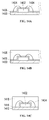
- FIG. 9A and FIG. 9B the translucent layer 900 is made by molding epoxy resin to form a flat surface, as shown in FIG. 9A .
- translucent layer 900 also has a flat surface as shown in FIG. 9B .
- the fluorescent layer and the translucent layer may have their lateral surface provided with reflective portions, as shown in FIG. 10A through FIG. 10C .
- a tool 1000 is used to cut the semi-cured fluorescent resin 504 and the translucent resin 900, so as to create grooves 1002, as shown in FIG. 10A . Then the grooves 1002 are filled with the reflective material 1004, as shown in FIG. 10B . Afterward, curing is performed as an optional step. At last, the reflective material 1004 and the carrier 500 are cut in a subsequent or simultaneous manner, thereby forming the light emitting device as shown in FIG. 10C .
- the light emitting device has the LED chip 502 deposited on the substrate 510, the fluorescent layer 514 conformally coated thereon, and the translucent layer 910 with a flat surface, while the reflective portions 1014 are formed at the opposite lateral surfaces of the fluorescent layer 514 and the opposite lateral surface of the translucent layer 910.
- the fluorescent layer 304 extends to the edges of the substrate 510 and is level with the edges of the substrate 510. However, in some variant examples, the fluorescent layer does not extend to the edges of the substrate, as shown in FIG. 11A and FIG. 11B .
- the fluorescent layer 1110 does not extend to edges to the substrate 510, so the surface of the substrate 510 is partially exposed. This reduces the risk that the fluorescent layer 1110 may be lifted at the edges of the substrate 510.
- a translucent layer 1112 may be provided outside the fluorescent layer 1110. In this case the translucent layer 1112 fully covers the fluorescent layer 1110, so as to further enhance resistance of the fluorescent material 1110 to moisture and oxygen.
- lateral surfaces of the translucent layer 1112 are level with lateral surface of the substrate 510.
- the present invention is not limited to this configuration, and the lateral surface of the translucent layer 1112 may be not level with that of the substrate 510.
- the present invention has no limitation to the method that prevents the fluorescent layer from extending to the edges of the substrate.
- the fluorescent layer may be precut after laminated in the step of FIG. 5C so that grooves are formed to expose parts of the carrier surface. Subsequently, as shown in FIG. 5D , singulation is performed on the carrier along these grooves. In another embodiment, after the singulation step as depicted in FIG. 5D , cutting is performed to single light emitting device for removing the parts of fluorescent layer that cover the edges of the substrate so as to expose the substrate surface at its edges.
- a precut semi-cured fluorescent resin is provided in the step of FIG. 5B . The fluorescent resin is such precut that traces instead of grooves are formed thereon. Later, when the laminating step of FIG. 5C is performed, the fluorescent resin separates into pieces along the traces under stress. Thus, during later singulation, there is no need to cut the fluorescent layer performed, thereby eliminating the risk of separation between the fluorescent layer and the substrate.
- the fluorescent layer is conformally coated on the LED chip and the substrate, its thickness is unnecessarily uniform.
- the fluorescent layer has a variable thickness, as shown in FIG. 12 .
- the fluorescent layer 1210 has v cuts 1212a, 1212b formed above the chip 502 and above the substrate 510, respectively, for providing varied light emitting effects.
- the present invention has no limitation to variation of thickness.
- cuts or bulges of various shapes as local shape modifications may be formed in the fluorescent layer 1210.
- its surface may be locally roughened.
- the number and locations of the shape modifications may be adapted to practical needs.
- the present invention has no limitation to the method for forming these local shape modifications and any suitable approaches may be implemented.
- a tool may be used to form cuts on the cured fluorescent layer.
- the mixture is applied to a plane having a rough surface at the stage of formation of the thin layer, so that the formed semi-cured fluorescent layer has a corresponded rough surface.
- the encapsulation resin for minimizing degradation of the fluorescent material, it is preferable to use a resin composition having its moisture permeability below 11 g/m 2 /24Hr and having its oxygen permeability below 400 cm 3 /m 2 /24Hr as the encapsulation resin (referred to the fluorescent layer and/or the translucent layer with the conformal process).
- a resin composition having its moisture permeability below 11 g/m 2 /24Hr and having its oxygen permeability below 400 cm 3 /m 2 /24Hr
- such encapsulation resin provides excellent protection to tetravalent-manganese-activated fluorescent materials. The following experiment is discussed for explaining the benefits of the encapsulation resin.
- FIG. 17 shows an encapsulating experiment.
- the light emitting device 1700 includes a light emitting chip 1702, a dispensing resin 1704 and a red fluorescent material 1706.
- the dispensing resin 1704 covers the light emitting chip 1702, and the red fluorescent material 1706 is distributed within the encapsulation resin 1704.
- the red fluorescent material may be a tetravalent-manganese-activated fluorescent material, with its chemical structure as described previously.
- the support 1708 may be formed with a structure different from that shown in FIG. 17 according to the actual design of the light emitting device.
- a substrate/carrier as described previously may be used as the support and the resin composition having those characteristics as described previously may be used to form the fluorescent layer, so as to protect the tetravalent-manganese-activated fluorescent material mixed therein.
- the aforementioned resin composition may be used to form the translucent layer and applied to the fluorescent layer having the tetravalent-manganese-activated fluorescent material. This make the translucent layer have its moisture permeability and oxygen permeability smaller than or equal to those of the fluorescent layer, thereby endowing the translucent layer with equal or even better ability to prevent permeation or absorption of moisture/oxygen.
- the light emitting chip 1702 is configured to emit a first light beam 1703, which excites the red fluorescent material 1706 to emit a second light beam 1707.
- an oxynitride fluorescent material may be further added, as shown in FIG. 18 .
- an oxynitride fluorescent material 1802 added into the dispensing resin 1704.
- the oxynitride fluorescent material 1802 has its chemical formula as that described previously.
- the dispensing resin may be a phenyl siloxane resin composition or a methyl siloxane resin composition.
- the dispensing resin has its refractive index above for example 1.5, and preferably between 1.5 and 1.6.
- the dispensing resin may contain the foregoing fluorescent material, and may additionally contain a staining agent, a light diffusion agent, a filler and/or other additives.
- a 450 nm-light beam was selected to identify the emission spectrum of a red fluorescent material of CaAlSiN 3 :Eu 2+ (acquired from NEMOTO Company, Japan), and the result is shown in FIG. 19 .
- a 450 nm-light beam was selected to identify the emission spectrum of a red fluorescent material K 2 Si 0.95 F 6 :Mn 4+ 0.05 of the present invention, and the result is shown in FIG. 19 .
- Comparative Example 1 has a wide emission spectrum extending to 750 nm. It emitted red light of low purity and low luminous intensity, which would in turn have adverse impact on luminous efficacy of white light.
- the red fluorescent material K 2 Si 0.95 F 6 :Mn 4+ 0.05 compound of the present invention had its emission mainly within the range of 600nm ⁇ 650 nm, so it overcomes the defects of commercial red fluorescent materials.
- Encapsulation Resin A phenyl-based silicone, moisture permeability of 10.5 g/m 2 /24Hr; oxygen permeability of 382 cm 3 /m 2 /24Hr) that a ratio between the weight of the resin and the total weight of the powder came to 1: 0.8.
- the encapsulation resin contained the fluorescent material was then used to encapsulate an InGaN chip.
- FIG. 21 is a chromaticity diagram of Experimental Example 3, the light after a color filter has an NTSC color gamut value of 84%.
- Sr 7 (Si,Al) 12 (O,N,C) 25 : Eu 2+ and K 2 Si 0.95 F 6 :Mn 4+ 0.05 were mixed at a weight ratio of 1: 1 and then added into Encapsulation Resin B (phenyl-based silicone, having moisture permeability of 15 g/m 2 /24Hr and oxygen permeability of 726 cm 3 /m 2 /24Hr) so the weight of the resin and the total weight of the powder came to a ratio at 1: 0.8.
- the encapsulation resin contained the fluorescent material was then used to encapsulate an InGaN chip.
- Term #2 driving current of 150 mA, temperature of 25°C, in atmosphere.
- Term #3 driving current of 150 mA, temperature of 25°C, in atmosphere.
- Term #4 driving current of 45 mA, temperature of 85°C, in atmosphere.
- ⁇ IV reduction in brightness as compared to initial brightness, expressed in percentage.
- ⁇ X CIE X coordinate deviation from initial brightness.
- ⁇ Y CIE Y coordinate deviation from initial brightness.
- the present invention can not only expand the color gamut of a TV backlight source, but also prevent the red fluorescent material from hydrolysis and degradation, thereby improving overall reliability of the disclosed light emitting device.
- fluorescent materials of other colors may be used additionally to further expand the color gamut of a backlight source.
- the following description is directed to a case where the chip of the light emitting device requires wiring, namely the case where a horizontal chip or a vertical chip is used in the disclosed light emitting device.
- a conductive wire has to be provided to connect the upper surface of the chip with the circuit pattern of the substrate.
- a conventional approach of applying rigid resin onto the conductive wire is likely to break the wire.
- the present invention differently uses the semi-cured fluorescent resin as the precursor of the fluorescent layer, so the semi-cured fluorescent resin conforms its own shape to the conductive wire.
- the conductive wire may run through, so as to not break due to application of the resin.
- the cured fluorescent layer then serves as a buffer between the subsequently applied translucent layer or other external material and the conductive wire for absorbing stress so as to protect the conductive wire, or protect the connection between the chip and the electrodes.
- the fluorescent layer is conformally coated on the conductive wire.
- a void portion may be formed below the conductive wire.
- the fluorescent layer flanks the conductive wire from two sides of the void portion.
- no void portion is formed below the conductive wire, and thus the fluorescent layer can fully embrace conductive wire.
- the conductive wire has its highest point, or its apogee, passing through the fluorescent layer. In this case the ends of the conductive wire that are connected to the chip are embraced by the fluorescent layer.
- FIG. 13 and FIG. 14 are provided for illustrating various embodiments involving such conductive wire.
- wire bonding is performed to connect one end of at least one conductive wire 1304 with the upper surface of the LED chip 1302, and connect an opposite end of the conductive wire 1304 with a conductive pattern (not shown) of the carrier 1300, as shown in FIG. 13A .
- a semi-cured fluorescent resin 1306 is provided and laminating operation is performed. After lamination, the semi-cured fluorescent resin 1306 conformally covers the conductive wire 1304, meaning that in a top view of the assembly the semi-cured fluorescent resin 1306 flasks the conductive wire 1304 from two sides thereof.
- a void portion may be formed below the conductive wire, as shown in FIG. 13B .
- the void portion 1308 below conductive wire 1304 acts as a stress buffer inside the light emitting device, for dealing with the bulk stress generated when the resin 1306 expands under heat. While in FIG.
- a translucent resin 1309 is applied onto the semi-cured fluorescent resin 1306 and cured, as shown in FIG. 13C .
- the translucent resin 1309 is preferably a rigid resin layer, such as epoxy resin.
- singulation is performed to subsequently or simultaneously cut the cured translucent resin 1309, the fluorescent resin 1306 and the carrier 1300, thereby forming the light emitting device as shown in FIG. 13D .
- the translucent layer 1319 covers the fluorescent layer 1316, and the fluorescent layer 1316 conformally covers the conductive wire 1304, while the void portion 1308 is formed below the conductive wire 1304. While FIG.
- 13D depicts a light emitting device having the void portion 1308, the present invention in some embodiments however has no such void portion and is so made that the fluorescent layer fully embraces the conductive wire.
- reflective portions as shown in FIG. 10C may be added to improve light convergence.
- the conductive wire may pass through the fluorescent layer.
- the conductive wire has its highest point, or its apogee, passing through the fluorescent layer, and the two ends of the conductive wire that are connected to the LED chip and the light emitting device, respectively, may be embraced by the fluorescent layer, as shown in FIG. 14A through FIG. 14C .
- a semi-cured fluorescent resin 1406 is provided and laminating operation is performed.
- the conductive wire 1404 runs through the semi-cured fluorescent resin 1406, meaning that in a lateral view of the assembly the semi-cured fluorescent resin 1406 is conformally coated on the surface of the LED chip 1402 and embrace both the two ends of the conductive wire 1404, as shown in FIG. 14A .
- a translucent resin 1408 is provided on the semi-cured fluorescent resin 1406 before curing is performed, as shown in FIG. 14B .
- the resin 1408 is preferably a rigid one, e.g. epoxide.
- singulation is performed by subsequently or simultaneously cutting the cured translucent layer 1418 and the substrate 1410, so as to form the light emitting device as shown in FIG. 14C .
- the conductive wire 1404 runs through the fluorescent layer 1416, and has parts, namely two ends thereof, covered by the fluorescent layer 1416.
- reflective portions as shown in FIG. 10C may be added to improve light concentration.
- a wired chip may be used in the embodiment as shown in FIG. 7B .
- the reflective portion and the light emitting diode chip are level with each other, or the reflective portion is higher than the LED chip while the fluorescent layer is coated on the reflective portion.
- the light emitting device further includes at least one conductive wire for connecting the LED chip with the electrodes in the light emitting device.
- the fluorescent layer embraces a part of the conductive wire, and the reflective portion embraces another part of the conductive wire.
- a light emitting device made using anisotropic conductive adhesive (ACA) and a molding process according to the present invention is now discussed. Reference is first made to FIG. 15 for the discussed manufacturing process. It is to be noted that while the metal leadframe is herein used as the carrier/substrate, implementation of the present invention is not limited thereto, and a PCBs or other materials may be used instead.
- ACA anisotropic conductive adhesive
- Step 1 a metal leadframe 1500 is provided on the release film, wherein the lateral surfaces of the metal leadframe 1500 may partially or fully embedded in the release film ( FIG. 15A ).
- Step 2 ACA 1502 is deposited on the metal leadframe 1500 ( FIG. 15B ).
- Step 3 the ACA 1502 fixes the LED chip 1504 to the metal leadframe 1500 ( FIG. 15C ).
- semi-cured fluorescent resin 1506 that can be placed on the surface of the LED chip 1504 is provided as a conformal pattern.
- the semi-cured fluorescent resin 1506 may extend to cover the lateral surface of the ACA 1502 and the lateral surface of the metal leadframe 1500 if necessary ( FIG. 15D ). Additionally, the semi-cured fluorescent resin 1506 contains the fluorescent material.
- Step 5 translucent resin 1508 is provided on the semi-cured fluorescent resin 1506 ( FIG. 15E ).
- Step 6 singulation is performed to form a plurality of light emitting devices ( FIG. 15F ).
- the light emitting device comprises a substrate that includes a pair of electrode pads 1600, 1602, preferably the substrate is constructed from a pair of electrode pads; an LED chip 1604, the fluorescent layer 1616, the translucent layer 1618 and the anisotropic conductive adhesive (ACA) 1610, 1612.
- the LED chip 1604 is exemplarily a flip chip and is bonded to the electrode pads 1600, 1602 by means of die bonding. That is the LED chip 1604 is directly electrically connected to the electrode pads 1600, 1602, without using conductive wire.
- the ACA 1610 on the electrode pad 1600 and the ACA 1612 on the electrode pad 1602 are separated from each other.
- the fluorescent layer 1616 conformally covers the LED chip 1604, the ACA 1610, 1612 and the electrode pads 1600, 1602, and extends to cover parts of the lateral surface 1600a, 1602a of the electrode pads 1600, 1602.
- the translucent layer 1618 covers the fluorescent layer 1616, with its lateral surface 1618a level with the lateral surface 1616a of the fluorescent layer 1616.
- the metal leadframe is not fully embedded in the release film (not shown), but only has parts of the electrode pads 1600, 1602 embedded. Thus, parts of the electrode pads 1600, 1602 are covered by the release film, while the other parts are covered by the fluorescent layer 1616. After removal of the release film, the parts previously covered by the release film are exposed and free from the fluorescent layer 1616 and the translucent layer 1618.
- the lateral surface 1616a of the fluorescent layer 1616 and the lateral surface 1618a of the translucent layer 1618 are not level with lateral surface 1600a, 1602a of the electrode pads 1600, 1602.
- ACA 1606 continues to cover both the P-type electrode pad 1600 and the N-type electrode pad 1602, thereby reflecting light at the bottom of the chip 1604 well without the risk of short circuit. It is to be noted that because of the characteristics of ACA, although the ACA 1606 in this variant example is in a continuous form, electric conduction is limited to the regions between the electrodes 1614 of the chip 1604 and the electrode pads 1600, 1602 and anywhere else remains electric insulation. This secures the light emitting device from short circuit.
- the electrode pads 1600, 1602 are fully embedded into the release film.
- the lateral surface 1600a and the bottom 1600b of the electrode pad 1600 and the lateral 1602a and the bottom 1602b of the electrode pad 1602 are fully exposed outside the fluorescent layer 1616 and the translucent layer 1618.
- the fluorescent layer 1616 extends over the electrode pads 1602 and 1612, as shown in FIG. 16C .
- ACA 1610, 1612 may be of any structure without limitation, and may be what shown in FIG. 16A or FIG. 16B .
- the lateral surface 1600a, 1602a of the electrode pads 1600, 1602 are level with the lateral surface 1616a of the fluorescent layer 1616 and the lateral 1618a of the translucent layer 1618, respectively, as shown in FIG. 16D .
- the fluorescent layer 1616 contains the fluorescent material
- the translucent layer 1618 and the fluorescent layer 1616 have their lateral surfaces level with each other, some converted light would be directly emitted from the lateral surface of the fluorescent layer 1616, leading to inconsistent light color.
- the translucent layer 1618 extends to cover the lateral surface 1616a of the fluorescent layer 1616 and is not level with the bottoms of the electrode pads 1600, 1602, as shown in FIG. 16E .
- the fluorescent layer 1616 may extend into the space 1608 between the P-type electrode pad 1600 and the N-type electrode pad 1602, as shown in FIG. 16F .
- the fluorescent layer 1616 may extend to entirely cover the lateral surface 1600a, 1602a of the electrode pads 1600, 1602. Additional application of the resin thus helps to enhance the mechanical strength of the light emitting device.
- external force may be used to make the fluorescent layer 1616 enter the space between the electrode pads 1600, 1602 or extend to cover the electrode pads 1600, 1602, so that after cured the fluorescent layer contributes to improve the mechanical strength of the light emitting device and protect the ACA 1610, 1612.
- a space filler 1620 may be provided at the lateral surface 1600a, 1602a of the electrode pads 1600, 1602 and filled into the space 1608. Referring to FIG. 16H , the lateral surface 1600a, 1602a and the space 1608 all have the space filler 1620 therewith. The lateral surface 1616a of the fluorescent layer 1616 and the lateral surface 1618a of the translucent layer 1618 are level with the lateral surface 1620a of the space filler 1620.
- the ACF 1622 may be formed in various ways, such as printing or coating.
- the ACF 1622 may comprise the reflective particles named above for better reflectivity. Where the applied area of the ACF 1622 is greater than the combined area of the LED chip 1604 and the electrode pads 1600, 1602, light extraction efficiency is further enhanced.
- the area of the ACF 1622 mat be of the same size as the area of the electrode 1614 of the chip 1604, as shown in FIG. 16I . However, for simplifying operation, the area of the ACF 1622 may be slightly greater than that of the electrode 1614 of the chip 1604, or even equal to the area of the electrode pads 1600, 1602, as shown in FIG. 16J . In the latter case, the lateral surface of the ACF 1622 are level with lateral surfaces of the light emitting layer 1618, the fluorescent layer 1616 and the electrode pads 1600, 1602. In addition, ACF is unnecessarily consistent with that of the P-type electrode pad or the N-type electrode pad (e.g. being square), and may be of any shape as long as it provides enough combining area.
- the light emitting device as shown in FIG. 16A through FIG. 16J uses ACA, it may use ACF instead of ACA and has the same appearance and form.
- a method for manufacturing a light emitting device using ACF comprises the following steps:
- the exemplary process described previously relates to use of a chip already having ACF (Step 2), it is apparent to people with ordinary skill in the art that the present invention is not limited thereto.
- the ACF may be applied to the electrode pad/support before die bonding is performed thereon for the LED chip.
Landscapes
- Led Device Packages (AREA)
Applications Claiming Priority (3)
| Application Number | Priority Date | Filing Date | Title |
|---|---|---|---|
| TW104120755 | 2015-06-26 | ||
| US201562211002P | 2015-08-28 | 2015-08-28 | |
| US201562248313P | 2015-10-30 | 2015-10-30 |
Publications (2)
| Publication Number | Publication Date |
|---|---|
| EP3109908A2 true EP3109908A2 (de) | 2016-12-28 |
| EP3109908A3 EP3109908A3 (de) | 2017-03-22 |
Family
ID=56263561
Family Applications (1)
| Application Number | Title | Priority Date | Filing Date |
|---|---|---|---|
| EP16176228.1A Withdrawn EP3109908A3 (de) | 2015-06-26 | 2016-06-24 | Lichtemittierende vorrichtung und herstellungsverfahren dafür |
Country Status (6)
| Country | Link |
|---|---|
| US (1) | US20160380162A1 (de) |
| EP (1) | EP3109908A3 (de) |
| JP (1) | JP2017034237A (de) |
| KR (1) | KR20170001637A (de) |
| CN (1) | CN106299080A (de) |
| TW (1) | TW201725763A (de) |
Families Citing this family (13)
| Publication number | Priority date | Publication date | Assignee | Title |
|---|---|---|---|---|
| US10256218B2 (en) * | 2017-07-11 | 2019-04-09 | Samsung Electronics Co., Ltd. | Light emitting device package |
| JP2019029603A (ja) * | 2017-08-03 | 2019-02-21 | 日亜化学工業株式会社 | 発光装置 |
| CN107629791B (zh) * | 2017-09-11 | 2020-09-25 | 苏州美纳福健康科技有限公司 | 一种Mn4+离子掺杂的红色荧光粉、制备方法及应用 |
| US10720554B2 (en) * | 2017-09-20 | 2020-07-21 | General Electric Company | Green-emitting phosphors and devices thereof |
| CN109904301A (zh) * | 2017-12-11 | 2019-06-18 | 深圳市聚飞光电股份有限公司 | 芯片级封装多面发光led及其封装方法、背光模组 |
| CN108417683A (zh) * | 2018-01-22 | 2018-08-17 | 东莞中之光电股份有限公司 | 一种倒裝led汽车灯的封装方法 |
| JP7002665B2 (ja) * | 2018-02-12 | 2022-02-04 | シグニファイ ホールディング ビー ヴィ | フッ化物蛍光体を有するled光源 |
| CN110322782B (zh) * | 2018-03-28 | 2021-12-07 | 英属开曼群岛商镎创科技股份有限公司 | 显示基板与显示面板 |
| TWI662521B (zh) * | 2018-03-28 | 2019-06-11 | PlayNitride Inc. | 顯示基板與顯示面板 |
| JP7243330B2 (ja) * | 2019-03-15 | 2023-03-22 | 市光工業株式会社 | 発光素子及び車両用灯具、並びに発光素子の製造方法 |
| TWI720785B (zh) * | 2020-01-15 | 2021-03-01 | 東貝光電科技股份有限公司 | 微型led發光裝置及其製造方法 |
| CN113087946B (zh) * | 2021-04-07 | 2021-12-14 | 昆明理工大学 | 一种基于应力发光材料的可重复记忆型应力薄膜的制备方法 |
| US12426423B2 (en) | 2022-05-09 | 2025-09-23 | Hefei BOE Ruisheng Technology Co., Ltd. | Light-emitting substrate, backlight module and display apparatus |
Citations (1)
| Publication number | Priority date | Publication date | Assignee | Title |
|---|---|---|---|---|
| US20140239328A1 (en) * | 2013-02-22 | 2014-08-28 | Samsung Electronics Co., Ltd. | Light emitting device package |
Family Cites Families (31)
| Publication number | Priority date | Publication date | Assignee | Title |
|---|---|---|---|---|
| US7157745B2 (en) * | 2004-04-09 | 2007-01-02 | Blonder Greg E | Illumination devices comprising white light emitting diodes and diode arrays and method and apparatus for making them |
| JP2007134376A (ja) * | 2005-11-08 | 2007-05-31 | Akita Denshi Systems:Kk | 発光ダイオード装置及びその製造方法 |
| US20070215998A1 (en) * | 2006-03-20 | 2007-09-20 | Chi Lin Technology Co., Ltd. | LED package structure and method for manufacturing the same |
| JP2008071955A (ja) * | 2006-09-14 | 2008-03-27 | Nichia Chem Ind Ltd | 発光装置 |
| US8940561B2 (en) * | 2008-01-15 | 2015-01-27 | Cree, Inc. | Systems and methods for application of optical materials to optical elements |
| TWI381556B (zh) * | 2009-03-20 | 2013-01-01 | 億光電子工業股份有限公司 | 發光二極體封裝結構及其製作方法 |
| WO2011093454A1 (ja) * | 2010-01-29 | 2011-08-04 | シチズン電子株式会社 | 発光装置の製造方法及び発光装置 |
| JP5442554B2 (ja) * | 2010-07-22 | 2014-03-12 | シチズンホールディングス株式会社 | 発光ダイオードの製造方法 |
| JP5519440B2 (ja) * | 2010-08-03 | 2014-06-11 | 日東電工株式会社 | 発光装置 |
| TW201216526A (en) * | 2010-08-20 | 2012-04-16 | Koninkl Philips Electronics Nv | Lamination process for LEDs |
| US9166126B2 (en) * | 2011-01-31 | 2015-10-20 | Cree, Inc. | Conformally coated light emitting devices and methods for providing the same |
| US20120236529A1 (en) * | 2011-03-15 | 2012-09-20 | Avago Technologies Ecbu Ip(Singapore) Pte. Ltd. | Method And Apparatus For A Light Source |
| JP5962102B2 (ja) * | 2011-03-24 | 2016-08-03 | 日亜化学工業株式会社 | 発光装置及びその製造方法 |
| US8957430B2 (en) * | 2011-06-15 | 2015-02-17 | Cree, Inc. | Gel underfill layers for light emitting diodes |
| JP6207402B2 (ja) * | 2012-02-02 | 2017-10-04 | シチズン時計株式会社 | 発光装置 |
| CN103311380A (zh) * | 2012-03-08 | 2013-09-18 | 展晶科技(深圳)有限公司 | 半导体封装制程及其封装结构 |
| JP2014036083A (ja) * | 2012-08-08 | 2014-02-24 | Toshiba Corp | 半導体発光装置 |
| KR20140095395A (ko) * | 2013-01-24 | 2014-08-01 | 삼성전자주식회사 | 반도체 발광소자 및 발광장치 |
| DE112014002056B4 (de) * | 2013-04-20 | 2023-06-01 | Mtek-Smart Corp. | Aufbring- oder Abgebeverfahren für Pulver oder körniges Material |
| CN203205458U (zh) * | 2013-04-22 | 2013-09-18 | 华中科技大学 | 一种led封装基板 |
| DE102013207611A1 (de) * | 2013-04-25 | 2014-10-30 | Osram Gmbh | Beleuchtungsvorrichtung mit optoelektronischem Bauelement |
| US9923132B2 (en) * | 2013-05-24 | 2018-03-20 | Cree, Inc. | Solid state lighting component package with conformal reflective coating |
| DE102013107862A1 (de) * | 2013-07-23 | 2015-01-29 | Osram Opto Semiconductors Gmbh | Oberflächenmontierbares optoelektronisches Halbleiterbauteil und Verfahren zur Herstellung zumindest eines oberflächenmontierbaren optoelektronischen Halbleiterbauteils |
| CN203406327U (zh) * | 2013-07-30 | 2014-01-22 | 简稚文 | 发光二极管的封装结构 |
| JP6209949B2 (ja) * | 2013-11-13 | 2017-10-11 | 日亜化学工業株式会社 | 発光装置及び発光装置の製造方法 |
| JP6237181B2 (ja) * | 2013-12-06 | 2017-11-29 | 日亜化学工業株式会社 | 発光装置の製造方法 |
| US20150226385A1 (en) * | 2014-02-11 | 2015-08-13 | Cree, Inc. | Systems and Methods for Application of Coatings Including Thixotropic Agents onto Optical Elements, and Optical Elements Having Coatings Including Thixotropic Agents |
| KR20150106488A (ko) * | 2014-03-11 | 2015-09-22 | 삼성디스플레이 주식회사 | 백라이트 유닛 및 이의 제조 방법 |
| JP6540026B2 (ja) * | 2014-12-26 | 2019-07-10 | 日亜化学工業株式会社 | 発光装置 |
| US20160276546A1 (en) * | 2015-03-18 | 2016-09-22 | Genesis Photonics Inc. | Chip package structure and method of manufacturing the same |
| KR20160130919A (ko) * | 2015-05-04 | 2016-11-15 | 삼성전자주식회사 | 발광다이오드 패키지 |
-
2016
- 2016-06-23 TW TW105119706A patent/TW201725763A/zh unknown
- 2016-06-23 US US15/190,214 patent/US20160380162A1/en not_active Abandoned
- 2016-06-24 JP JP2016125954A patent/JP2017034237A/ja active Pending
- 2016-06-24 KR KR1020160079213A patent/KR20170001637A/ko not_active Withdrawn
- 2016-06-24 CN CN201610472120.0A patent/CN106299080A/zh active Pending
- 2016-06-24 EP EP16176228.1A patent/EP3109908A3/de not_active Withdrawn
Patent Citations (1)
| Publication number | Priority date | Publication date | Assignee | Title |
|---|---|---|---|---|
| US20140239328A1 (en) * | 2013-02-22 | 2014-08-28 | Samsung Electronics Co., Ltd. | Light emitting device package |
Also Published As
| Publication number | Publication date |
|---|---|
| CN106299080A (zh) | 2017-01-04 |
| US20160380162A1 (en) | 2016-12-29 |
| EP3109908A3 (de) | 2017-03-22 |
| KR20170001637A (ko) | 2017-01-04 |
| TW201725763A (zh) | 2017-07-16 |
| JP2017034237A (ja) | 2017-02-09 |
Similar Documents
| Publication | Publication Date | Title |
|---|---|---|
| EP3109908A2 (de) | Lichtemittierende vorrichtung und herstellungsverfahren dafür | |
| US10588184B2 (en) | Light emitting device and LED package structure | |
| JP4667803B2 (ja) | 発光装置 | |
| JP4451178B2 (ja) | 発光デバイス | |
| JP5123466B2 (ja) | 発光装置 | |
| JP7727121B2 (ja) | 異なる色度のledを有する照明デバイス | |
| JP5329060B2 (ja) | 発光体およびこれを用いた光デバイス | |
| JP6396295B2 (ja) | 光源装置および発光装置 | |
| JP4337574B2 (ja) | 発光装置およびその形成方法 | |
| JP4350183B2 (ja) | 半導体発光装置 | |
| CN102044622B (zh) | 发光二极管及其制作方法 | |
| JP4650378B2 (ja) | 発光装置の製造方法 | |
| US20120001214A1 (en) | Phosphor ceramic and light-emitting device | |
| JP4591071B2 (ja) | 半導体装置 | |
| JP4855869B2 (ja) | 発光装置の製造方法 | |
| JP2017188592A (ja) | 発光装置 | |
| KR20180090260A (ko) | 형광체 시트, 그것을 사용한 발광체, 광원 유닛, 디스플레이 및 발광체의 제조 방법 | |
| JP5315607B2 (ja) | 発光装置及びその製造方法 | |
| JP5619533B2 (ja) | 発光装置 | |
| TW200814379A (en) | Luminescent light source and method for manufacturing the same | |
| JP2018191015A (ja) | 発光装置の製造方法 | |
| CN114361142A (zh) | 一种高亮led组件及其加工工艺与应用 | |
| JP2017220530A (ja) | 発光装置の製造方法 |
Legal Events
| Date | Code | Title | Description |
|---|---|---|---|
| PUAI | Public reference made under article 153(3) epc to a published international application that has entered the european phase |
Free format text: ORIGINAL CODE: 0009012 |
|
| STAA | Information on the status of an ep patent application or granted ep patent |
Free format text: STATUS: THE APPLICATION HAS BEEN PUBLISHED |
|
| AK | Designated contracting states |
Kind code of ref document: A2 Designated state(s): AL AT BE BG CH CY CZ DE DK EE ES FI FR GB GR HR HU IE IS IT LI LT LU LV MC MK MT NL NO PL PT RO RS SE SI SK SM TR |
|
| AX | Request for extension of the european patent |
Extension state: BA ME |
|
| PUAL | Search report despatched |
Free format text: ORIGINAL CODE: 0009013 |
|
| AK | Designated contracting states |
Kind code of ref document: A3 Designated state(s): AL AT BE BG CH CY CZ DE DK EE ES FI FR GB GR HR HU IE IS IT LI LT LU LV MC MK MT NL NO PL PT RO RS SE SI SK SM TR |
|
| AX | Request for extension of the european patent |
Extension state: BA ME |
|
| RIC1 | Information provided on ipc code assigned before grant |
Ipc: H01L 33/60 20100101ALI20170215BHEP Ipc: H01L 33/62 20100101ALI20170215BHEP Ipc: H01L 33/50 20100101AFI20170215BHEP |
|
| STAA | Information on the status of an ep patent application or granted ep patent |
Free format text: STATUS: REQUEST FOR EXAMINATION WAS MADE |
|
| 17P | Request for examination filed |
Effective date: 20170920 |
|
| RBV | Designated contracting states (corrected) |
Designated state(s): AL AT BE BG CH CY CZ DE DK EE ES FI FR GB GR HR HU IE IS IT LI LT LU LV MC MK MT NL NO PL PT RO RS SE SI SK SM TR |
|
| STAA | Information on the status of an ep patent application or granted ep patent |
Free format text: STATUS: EXAMINATION IS IN PROGRESS |
|
| 17Q | First examination report despatched |
Effective date: 20200330 |
|
| STAA | Information on the status of an ep patent application or granted ep patent |
Free format text: STATUS: THE APPLICATION IS DEEMED TO BE WITHDRAWN |
|
| 18D | Application deemed to be withdrawn |
Effective date: 20200811 |