EP3092501B1 - Compensation technique for amplifiers in a current sensing circuit for a battery - Google Patents
Compensation technique for amplifiers in a current sensing circuit for a battery Download PDFInfo
- Publication number
- EP3092501B1 EP3092501B1 EP15701441.6A EP15701441A EP3092501B1 EP 3092501 B1 EP3092501 B1 EP 3092501B1 EP 15701441 A EP15701441 A EP 15701441A EP 3092501 B1 EP3092501 B1 EP 3092501B1
- Authority
- EP
- European Patent Office
- Prior art keywords
- amplifier
- offset error
- phase
- during
- erramp2
- Prior art date
- Legal status (The legal status is an assumption and is not a legal conclusion. Google has not performed a legal analysis and makes no representation as to the accuracy of the status listed.)
- Not-in-force
Links
Images


Classifications
-
- G—PHYSICS
- G01—MEASURING; TESTING
- G01R—MEASURING ELECTRIC VARIABLES; MEASURING MAGNETIC VARIABLES
- G01R31/00—Arrangements for testing electric properties; Arrangements for locating electric faults; Arrangements for electrical testing characterised by what is being tested not provided for elsewhere
- G01R31/36—Arrangements for testing, measuring or monitoring the electrical condition of accumulators or electric batteries, e.g. capacity or state of charge [SoC]
- G01R31/374—Arrangements for testing, measuring or monitoring the electrical condition of accumulators or electric batteries, e.g. capacity or state of charge [SoC] with means for correcting the measurement for temperature or ageing
-
- G—PHYSICS
- G01—MEASURING; TESTING
- G01R—MEASURING ELECTRIC VARIABLES; MEASURING MAGNETIC VARIABLES
- G01R31/00—Arrangements for testing electric properties; Arrangements for locating electric faults; Arrangements for electrical testing characterised by what is being tested not provided for elsewhere
- G01R31/36—Arrangements for testing, measuring or monitoring the electrical condition of accumulators or electric batteries, e.g. capacity or state of charge [SoC]
- G01R31/382—Arrangements for monitoring battery or accumulator variables, e.g. SoC
- G01R31/3842—Arrangements for monitoring battery or accumulator variables, e.g. SoC combining voltage and current measurements
-
- G—PHYSICS
- G01—MEASURING; TESTING
- G01R—MEASURING ELECTRIC VARIABLES; MEASURING MAGNETIC VARIABLES
- G01R19/00—Arrangements for measuring currents or voltages or for indicating presence or sign thereof
- G01R19/0046—Arrangements for measuring currents or voltages or for indicating presence or sign thereof characterised by a specific application or detail not covered by any other subgroup of G01R19/00
-
- G—PHYSICS
- G01—MEASURING; TESTING
- G01R—MEASURING ELECTRIC VARIABLES; MEASURING MAGNETIC VARIABLES
- G01R19/00—Arrangements for measuring currents or voltages or for indicating presence or sign thereof
- G01R19/32—Compensating for temperature change
-
- H—ELECTRICITY
- H01—ELECTRIC ELEMENTS
- H01M—PROCESSES OR MEANS, e.g. BATTERIES, FOR THE DIRECT CONVERSION OF CHEMICAL ENERGY INTO ELECTRICAL ENERGY
- H01M10/00—Secondary cells; Manufacture thereof
- H01M10/42—Methods or arrangements for servicing or maintenance of secondary cells or secondary half-cells
- H01M10/48—Accumulators combined with arrangements for measuring, testing or indicating the condition of cells, e.g. the level or density of the electrolyte
-
- H—ELECTRICITY
- H03—ELECTRONIC CIRCUITRY
- H03F—AMPLIFIERS
- H03F3/00—Amplifiers with only discharge tubes or only semiconductor devices as amplifying elements
- H03F3/45—Differential amplifiers
- H03F3/45071—Differential amplifiers with semiconductor devices only
- H03F3/45076—Differential amplifiers with semiconductor devices only characterised by the way of implementation of the active amplifying circuit in the differential amplifier
- H03F3/45179—Differential amplifiers with semiconductor devices only characterised by the way of implementation of the active amplifying circuit in the differential amplifier using MOSFET transistors as the active amplifying circuit
-
- H—ELECTRICITY
- H03—ELECTRONIC CIRCUITRY
- H03F—AMPLIFIERS
- H03F3/00—Amplifiers with only discharge tubes or only semiconductor devices as amplifying elements
- H03F3/45—Differential amplifiers
- H03F3/45071—Differential amplifiers with semiconductor devices only
- H03F3/45076—Differential amplifiers with semiconductor devices only characterised by the way of implementation of the active amplifying circuit in the differential amplifier
- H03F3/45475—Differential amplifiers with semiconductor devices only characterised by the way of implementation of the active amplifying circuit in the differential amplifier using IC blocks as the active amplifying circuit
-
- H—ELECTRICITY
- H03—ELECTRONIC CIRCUITRY
- H03F—AMPLIFIERS
- H03F2203/00—Indexing scheme relating to amplifiers with only discharge tubes or only semiconductor devices as amplifying elements covered by H03F3/00
- H03F2203/45—Indexing scheme relating to differential amplifiers
- H03F2203/45048—Calibrating and standardising a dif amp
-
- H—ELECTRICITY
- H03—ELECTRONIC CIRCUITRY
- H03F—AMPLIFIERS
- H03F2203/00—Indexing scheme relating to amplifiers with only discharge tubes or only semiconductor devices as amplifying elements covered by H03F3/00
- H03F2203/45—Indexing scheme relating to differential amplifiers
- H03F2203/45138—Two or more differential amplifiers in IC-block form are combined, e.g. measuring amplifiers
-
- Y—GENERAL TAGGING OF NEW TECHNOLOGICAL DEVELOPMENTS; GENERAL TAGGING OF CROSS-SECTIONAL TECHNOLOGIES SPANNING OVER SEVERAL SECTIONS OF THE IPC; TECHNICAL SUBJECTS COVERED BY FORMER USPC CROSS-REFERENCE ART COLLECTIONS [XRACs] AND DIGESTS
- Y02—TECHNOLOGIES OR APPLICATIONS FOR MITIGATION OR ADAPTATION AGAINST CLIMATE CHANGE
- Y02E—REDUCTION OF GREENHOUSE GAS [GHG] EMISSIONS, RELATED TO ENERGY GENERATION, TRANSMISSION OR DISTRIBUTION
- Y02E60/00—Enabling technologies; Technologies with a potential or indirect contribution to GHG emissions mitigation
- Y02E60/10—Energy storage using batteries
Definitions
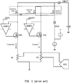
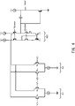
- FIG. 1 shows an example of a battery monitoring system or fuel gauge system.
- Battery current flows between a system node VSYS and a battery terminal VBATT through a main transistor (e.g., a transistor BATFET).
- a main transistor e.g., a transistor BATFET
- replica devices e.g., replica transistors Replica1 and Replica2
- the replica transistors Replica1 and Replica2 produce replica currents (e.g., a charging current I CHARGE and a discharge current I DISCHARGE ) that are a scaled down version of the battery current.
- the charging current I CHARGE and the discharge current I DISCHARGE flow through sensing resistors R1 and R2, respectively.
- An analog to digital converter (ADC) samples the voltage across resistors R1 and R2 to determine the charge across the battery.
- the battery monitoring system uses the output of the ADC to monitor the battery.
- the system may use a feedback loop to control the voltage.
- amplifiers AMP1 and AMP2 control the voltage across control transistors M1 and M2, respectively.
- the inputs of amplifier AMP1 are coupled to the system node VSYS and the gate and source of replica transistor Replica2 and the output is coupled to a control transistor M1.
- the inputs of amplifier AMP2 are coupled to the system node VBATT and the drain of replica transistor Replica1 and the output is coupled to a control transistor M2.
- Amplifiers AMP1 and AMP2 control the voltage at the gate of control transistors M1 and M2, respectively, to produce the replica currents.
- a circuit in one embodiment, includes a first amplifier having a first differential input, a second differential input, and an output.
- the first differential input is coupled to a replica device and a voltage of a battery and the output is coupled to a control device.
- the replica device is configured to generate a replica current of a current flowing through the battery where the first amplifier controls the control device to control the replica current.
- the circuit also includes a second amplifier having a third differential input, a fourth differential input, and an output.
- the second amplifier is configured to compensate for a first offset error of the first amplifier and a second offset error of the second amplifier based on selectively coupling the third differential input to the output of the first amplifier during a first phase, selectively coupling the output of the second amplifier to the second differential input during the first phase, and selectively coupling the output of the second amplifier to the fourth differential input during a second phase.
- the second amplifier stores the second offset error of the second amplifier on a first set of storage elements coupled to the fourth differential input of the second amplifier for use in compensating for the second offset error of the second amplifier during the first phase.
- the second amplifier stores the first offset error of the first amplifier on a second set of storage elements coupled to the second differential input of the first amplifier for use in compensating for the first offset error of the first amplifier during a subsequent second phase.
- a gain of the second amplifier is used to compensate for the first offset error during the first phase.
- the output of the second amplifier is a differential output
- the circuit further includes a common mode feedback circuit coupled to the differential output and configured to maintain a common mode portion of the differential output at a fixed value different from the voltage of the battery.
- the circuit further includes a resistor configured to receive the replica current, wherein a voltage across the resistor is sensed to monitor the voltage across the battery.
- a method includes: during a first phase, storing, by a second amplifier, a first offset error of a first amplifier on a first set of storage elements coupled to a differential input of the first amplifier for use in compensating for the first offset error of the first amplifier during a second phase; during the second phase, storing, by the second amplifier, a second offset error of the second amplifier on a second set of storage elements coupled to a differential input of the second amplifier for use in compensating for the second offset error of the second amplifier during a subsequent first phase; during the second phase, controlling, by the first amplifier, a control device to control a replica current generated by the replica device, the replica current being a replica of a current flowing through the battery, wherein the first offset error is compensated for using the first offset error stored during the first phase; and during the subsequent first phase, controlling, by the first amplifier, the control device to control the replica current, wherein a gain of the second amplifier is used to compensate for the first offset error and the second offset error is compensated for using the second offset error stored during
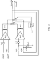
- FIG. 2 depicts an example of a battery monitoring system 200 according to one embodiment.
- Battery monitoring system 200 may monitor battery currents (e.g., discharging and charging currents) for a battery (BATT) 202 flowing through a transistor BATFET from a node VSYS to a node VBATT.
- BATT battery
- FIG. 2 only the charging current is shown, but a person skilled in the art will appreciate how to implement the battery monitoring system to monitor the discharging current.
- Battery monitoring system 200 may monitor the battery current using an internal (e.g., on chip) current-sensing resistor R 1 . Although an internal resistor is discussed, external (e.g., off chip) resistors may be used.
- System 200 uses a replica transistor Replica1 to generate a replica current of a battery current I B that flows through battery transistor BATFET and battery 202 through a node VBATT.
- transistors BATFET and replica1 may be N-channel MOSFET devices with their gate and sources coupled together. As shown, the replica current I CHARGE flows through transistor Replica1 and may be a scaled-down version of the battery current I B .
- Amplifiers ErrAmp1 and ErrAmp2 form a feedback loop that controls the voltage across a replica device, such as a control transistor M c , which operates in different operating regions (saturation or linear) depending on the mode of operation of a linear charger for battery 202.
- amplifier ErrAmp1 controls a gate voltage of control transistor M c to control the replica current I CHARGE through sensing resistor R 1 .
- the control of control transistor M c may regulate the replica current I CHARGE to be proportional to the battery current I B .
- an ADC (not shown) may measure the voltage across sensing resistor R 1 , where the output of the ADC is used by a battery management system or fuel gauge measurement algorithm.
- the offset error of the amplifiers may affect the performance of battery monitoring system 200.
- the replica current I CHARGE may be small and the voltage across sensing resistor R 1 may be as low as hundreds of microvolts.
- the offset error of amplifiers ErrAmp1 and ErrAmp2 may affect the measured voltage.
- Particular embodiments compensate for the amplifier offset error and also employ a technique to reduce the effect of temperature variations on resistor R 1 .
- amplifier ErrAmp1 may include a first differential input and a second differential input along with an output coupled to transistor M c .
- Amplifier ErrAmp2 may include a first differential input, a second differential input, and a differential output. Accordingly, amplifier ErrAmp1 and amplifier ErrAmp2 have two gain stages as will be described in more detail below. Although amplifier ErrAmp2 is described as having a differential output, amplifier ErrAmp2 may have a single output. As will be discussed in more detail below, the differential output allows system 200 the compensation to be performed at a different voltage than VBATT or a rail voltage of the system.
- Amplifier ErrAmp2 may be a nulling amplifier that is used to compensate for the offset error in the main amplifier ErrAmp1. Further, Amplifier ErrAmp2 also compensates for its own offset error. As will be discussed in more detail below, the technique may be used continuously to track changes in the offset error and effectively compensate for the changes in the offset error. Thus, amplifiers ErrAmp2 and ErrAmp1 can track any shift in the offset errors due to operating conditions and compensate for the errors (e.g., null or zero the errors). Thus, the compensation may be better than a one-time compensation.
- Battery monitoring system 200 may use multiple clock phases, such as a clock phase ⁇ 1 and a clock phase ⁇ 2, to compensate for the offset errors of amplifier ErrAmp1 and amplifier ErrAmp2.
- clock phase ⁇ 1 amplifier ErrAmp2 stores the offset error of amplifier ErrAmp1 on capacitors C1. This value will be used to compensate for the offset error of amplifier ErrAmp1 in a subsequent clock phase ⁇ 2.
- clock phase ⁇ 2 system 200 stores the offset error of amplifier ErrAmp2 on capacitors C2. This compensates for the offset error of amplifier ErrAmp2 in a subsequent clock phase ⁇ 1 as the stored offset error makes sure the offset error of amplifier ErrAmp2 does not affect the storing of the offset error of amplifier ErrAmp1 on capacitors C1.
- switches S1 and S2 may be open or closed based on the clock phase. For example, switches S1 are closed during clock phase ⁇ 1 and open during clock phase ⁇ 2, and switches S2 are closed during clock phase ⁇ 2, and open during clock phase ⁇ 1.
- the use of switches S1 and S2 couples the inputs and outputs of amplifiers ErrAmp1 and ErrAmp2 differently depending on the clock phase.
- FIG. 3 depicts an example of amplifier ErrAmp2 during clock phase ⁇ 2 according to one embodiment.
- switches S2 are closed and switches S1 are open, which isolate the input and output of amplifier ErrAmp2 from the input and output of amplifier ErrAmp1.
- amplifier ErrAmp2 may be in an open loop gain configuration.
- amplifier ErrAmp2 stores the offset error of amplifier ErrAmp2 on capacitors C2 during this clock phase.
- Amplifier ErrAmp2 includes a first amplifier An1 and a second amplifier An2 that receive a first differential input and a second differential input, respectively. Both inputs of the differential input of amplifier An1 are coupled to battery 102.
- the offset error of amplifier An1 is shown as an offset error voltage Von1 at the input of one of the differential inputs.
- a feedback path from the output of amplifier ErrAmp2 to the differential input of amplifier An2 is used.
- the output of amplifier ErrAmp2 e.g., differential output VonullN and VonullP
- capacitors C2 which can store the offset error during clock phase ⁇ 2.
- the offset error stored on capacitors C2 includes an inferred offset error voltage Von2 on one input of the differential input of amplifier An2 and the offset error voltage Von1.
- CMFB common mode feedback circuit
- the differential output may be the combination of vn1 + vn2, which reflect the offset errors Von1 and Von2.
- the outputs VonullN and VonullP are then stored on capacitors C2 during clock phase ⁇ 2.
- V ocm A CMFB 1 + A CMFB V ref
- V onullP V ocm + 1 2 v n 1 + v n 2
- the voltage of the common mode amplifier Acm is based on the gain of amplifier Acm and a voltage Vref. Voltage Vref may be different from the voltage of the battery or rail, such as Vdd/2.
- Equation 1 shows the calculation for output VonullP and equation 2 shows the calculation for output VonullN.
- output VonullP is the common mode output voltage Vocm plus half of the differential output of vn1 and vn2.
- Output VonullN is equal to the common mode voltage Vocm minus half of the differential output of vn1 and vn2.
- Equation 3 shows the calculation of the differential between outputs VonullN and VonullP and equations 4 and 5 show the calculation of the amplifier outputs of vn2 and vn1.
- equation 3 shows that the differential output ⁇ Vonull is equal to the amplifier outputs vn1 and vn2 as the common mode voltage Vocm cancels.
- Output vn2 is equal to the gain of amplifier An2 and the offset error of amplifier An2 minus the differential output.
- Output vn1 is equal to the gain of amplifier An1 and the offset error of amplifier An1.
- the differential output voltage ⁇ Vonull may be determined based on equations 3, 4, and 5. Equation 6 shows that the differential output of amplifier ErrAmp2 is based on the offset errors Von1 and Von2 of amplifiers An1 and An2 and the gain of error amplifiers An1 and An2. These values are stored on capacitors C2 during clock phase ⁇ 2. As will be discussed in the next figure, the values stored on capacitors C2 are used to cancel the offset errors Von1 and Von2 during the next clock phrase ⁇ 1.
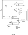
- FIG. 4 depicts an example of amplifiers ErrAmp1 (amplifiers A1 and A2) and ErrAmp2 (amplifiers An1 and An2) during clock phase ⁇ 1 according to one embodiment.
- switches S1 are closed and switches S2 are open.
- This couples the differential output of ErrAmp2 to a differential input of ErrAmp1.
- This stores the offset error for amplifier ErrAmp1 on capacitors C1 via amplifier ErrAmp2.
- the offset error of amplifier ErrAmp2 is canceled via the previous stored values on capacitors C2 in clock phase ⁇ 2 so that the amplifier ErrAmp2 offset error does not affect the storing of the values on capacitors C1.
- the following will now discuss the offset compensation in more detail.
- the inputs of amplifier A1 are coupled to the output Vout of amplifier ErrAmp1 and the voltage of battery 102.
- the offset error of amplifier A1 is shown as an offset error voltage Vo1 on one of the inputs of amplifier A1.
- the differential input of amplifier A2 is coupled to the differential output of amplifier ErrAmp2.
- the offset error of amplifier A2 is shown as an offset error voltage Vo2 on one of the inputs of amplifier A2.
- the differential output voltage of amplifier ErrAmp2 is equal to the gain of amplifier An1 times the difference between the battery voltage VBATT and the output voltage of amplifier ErrAmp1.
- the offset errors Von1 and Von2 of amplifiers An1 and An2 have been canceled in this case via the values stored on capacitors C2. That is, amplifier An2 cancels offset error Von2 and outputs offset error Von1 (e.g., Von1 times the gain of An2). This outputted offset error Von1 cancels the offset error from amplifier An1.
- equation 8 can be approximated to: V out ⁇ VBATT + A 1 A 1 + A 2 ⁇ A n 1 ⁇ v 01 + A 2 A 1 + A 2 ⁇ A n 1 ⁇ v 02 ⁇ VBATT
- FIG. 5 depicts an example of amplifier ErrAmp1 in clock phase ⁇ 2 according to one embodiment.
- the inputs of amplifier A1 are coupled to the output Vout of amplifier ErrAmp1 and to the battery voltage VBATT.
- the offset error voltage Vo1 is also shown at an input of amplifier A1.
- the inputs of amplifier A2 are coupled to capacitors C1.
- the offset error voltage Vo2 is also shown at an input of amplifier A2.
- capacitors C1 hold the differential voltage ⁇ Vonull1, which is based on the gain of amplifiers A1 and A2 and the offset errors of amplifiers A1 and A2 of Vo1 and Vo2.
- the differential output voltage of amplifier ErrAmp2 is equal to the gain of Amplifier An1 times the difference of VBATT and Vout.
- the values stored on capacitors C1 are a function of the gain of amplifiers A1 and A2 and the offset errors Vo1 and Vo2.
- Equation 11 represents the determination of the output voltage Vout of ErrAmp1, which shows the cancellation of offset errors Vo1 and Vo2 as follows:
- the offset errors Vo1 and Vo2 are cancelled and the output voltage Vout of amplifier ErrAmp1 approximately equals the battery voltage VBATT, Vout ⁇ VBATT.
- the values stored on capacitors C1 include offset errors Vo1 and Vo2.
- the offset error Vo2 stored on capacitor C1 cancels the offset error Vo2 of amplifier A2.
- amplifier A2 outputs offset error Vo1 amplified by the gain A2 of amplifier A2.
- amplifier A1 outputs offset error Vo1 amplified by the gain A1 of amplifier A1.
- the outputs of amplifiers A1 and A2 are of the opposite polarity and thus cancel offset error Vo1 when combined. Accordingly, the offset errors of Vo1 and Vo2 are cancelled in clock phase ⁇ 2 and output voltage Vout substantially equals the battery voltage VBATT.
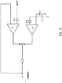
- FIGs. 6 and 7 show examples of implementations of ErrAmp1 and ErrAmp2, respectively. However, it will be understood that other implementations may be appreciated.
- differential amplifiers A1 and A2 are shown as a differential pair of transistors M A1 and a differential pair of transistors M A2 .
- Amplifiers A1 and A2 are coupled to a shared output stage 602.
- Shared output stage 602 provides a resistor gain that converts a current output of differential amplifiers A1 and A2 into a voltage output. Different variations of shared output stage 602 may be appreciated.
- differential amplifiers An1 and An2 are shown as a differential pair of transistors M AN2 and a differential pair of transistors M AN1 , respectively.
- the output of amplifiers An1 and An2 are coupled to a shared output stage 702.
- Shared output stage 702 also converts a current output of amplifiers An1 and An2 to a voltage, but the output of shared output stage 702 is a differential output Out- and Out+.
- a common mode feedback circuit 704 is coupled to the differential output and maintains an average value of the differential output at a fixed level based on a voltage Vref, which may be at a different level than the rail voltage, such as 1 ⁇ 2(Vdd).
- common mode feedback circuit 704 the differential voltage measurement is moved away from the rail voltage or battery voltage VBATT. For example, if the differential voltage measurement is close to the rail, then it might be hard to measure the differential voltage accurately. Thus, setting the common mode differential output voltage to a value, such as 1 ⁇ 2 of the rail voltage, makes calculating the offset at the average value more accurate. That is, outputs Out+ and Out- are both set at a common mode voltage. Then, the differential of outputs Out+ and Out- can be calculated based on that common mode value that is different from the rail voltage. The common mode voltage drops out while the differential voltage is output on outputs Out+ and Out-. Using the common mode voltage at around half the battery voltage VBATT may simplify the output stage 702.
- FIG. 8 shows an example of a battery monitoring system 800 using a single output of amplifier ErrAmp2 according to one embodiment.
- a single output of amplifier ErrAmp2 is coupled to amplifier ErrAmp1.
- the single output of amplifier ErrAmp2 is coupled to an input of amplifier ErrAmp2 in a feedback configuration.
- Another input of amplifier ErrAmp2 and another input of amplifier ErrAmp1 are coupled to a voltage Vref, which may be a voltage different from the rail voltage.
- the voltage stored across capacitors C2 includes the offset errors Von1 and Von2. In clock phase ⁇ 1, these stored offset errors compensate for the offset errors of amplifier ErrAmp2. Also, in clock phase ⁇ 1, Vout ⁇ VBATT due to the gain of amplifier An2 (not shown) of amplifier ErrAmp2 substantially canceling the offset errors of amplifier ErrAmp1. Further, in clock phase ⁇ 2, the offset error stored on capacitors C1 cancels the error of amplifier ErrAmp1.
- FIG. 9 depicts a simplified flowchart 900 of a method for compensating for offset error according to one embodiment.
- amplifier ErrAm2 stores a first offset error of amplifier ErrAmp 1 on capacitors C1 for use in compensating for the offset error of amplifier ErrAmplduring a second phase.
- amplifier ErrAmp2 stores an offset error of amplifier ErrAmp2 on capacitors C2 for use in compensating for the offset error of amplifier ErrAmp2 during a subsequent first phase.
- amplifier ErrAmp1 controls control transistor M C to control a replica current generated by the replica device.
- the first offset error is compensated for using the first offset error stored during the first phase.
- amplifier ErrAmp 1 controls control transistor M C to control the replica current where a gain of the second amplifier is used to compensate for the offset error of amplifier ErrAmp1 and the offset error of amplifier ErrAmp2 is compensated for using the offset error of amplifier ErrAmp2 stored on capacitors C2 during the second phase.
- sensing resistor R 1 may be located on chip and thus may be sensitive to temperature variations of the chip.
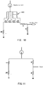
- FIG. 10 shows an example implementation of resistor R 1 to compensate for temperature variations according to one embodiment. The temperature variations may be compensated for during the current voltage conversion using two types of resistors.
- the first type of resistor R is a poly resistor with P+ doping having a negative temperature coefficient.
- the second type of resistors rsp are silicided and having a positive temperature coefficient. The opposite temperature coefficients can be used to compensate for temperature variations.
- the size of resistor rsp (e.g., rsp 1, rsp 2, rsp 3, ..., rsp N) can be adjusted via taps 1002. Different tap settings may be used to adjust for the temperature variation by opening or closing different taps to couple various resistors rsp to the replica current. The size of resistors rsp may then compensate for the temperature variation. For example, the size of resistors rsp will determine the final slope of the resistance with respect to temperatures.
- FIG. 11 depicts an example of the temperature correction using resistor rsp1 according to one embodiment.
- Resistor RSP in FIG. 10 represents the combination of resistors rsp1 - rspN that are coupled to the replica current based on the tap settings.
- Vout may be determined as follows: Vout ⁇ I / 2 R + 1 / 2 rsp .
- the output voltage Vout across sensing resistor R 1 is equal to the resistance of R that is compensated by the resistance of resistor rsp.
- internal resistors are discussed as being used, particular embodiments may also use external resistors that are off-chip and thus do not need temperature compensation.
Landscapes
- Physics & Mathematics (AREA)
- General Physics & Mathematics (AREA)
- Engineering & Computer Science (AREA)
- Power Engineering (AREA)
- Manufacturing & Machinery (AREA)
- Chemical & Material Sciences (AREA)
- Chemical Kinetics & Catalysis (AREA)
- Electrochemistry (AREA)
- General Chemical & Material Sciences (AREA)
- Amplifiers (AREA)
- Measurement Of Current Or Voltage (AREA)
Applications Claiming Priority (2)
| Application Number | Priority Date | Filing Date | Title |
|---|---|---|---|
| US14/149,739 US9217780B2 (en) | 2014-01-07 | 2014-01-07 | Compensation technique for amplifiers in a current sensing circuit for a battery |
| PCT/US2015/010529 WO2015105915A1 (en) | 2014-01-07 | 2015-01-07 | Compensation technique for amplifiers in a current sensing circuit for a battery |
Publications (2)
| Publication Number | Publication Date |
|---|---|
| EP3092501A1 EP3092501A1 (en) | 2016-11-16 |
| EP3092501B1 true EP3092501B1 (en) | 2017-09-13 |
Family
ID=52424124
Family Applications (1)
| Application Number | Title | Priority Date | Filing Date |
|---|---|---|---|
| EP15701441.6A Not-in-force EP3092501B1 (en) | 2014-01-07 | 2015-01-07 | Compensation technique for amplifiers in a current sensing circuit for a battery |
Country Status (6)
| Country | Link |
|---|---|
| US (1) | US9217780B2 (ko) |
| EP (1) | EP3092501B1 (ko) |
| JP (1) | JP6602766B2 (ko) |
| KR (1) | KR101740581B1 (ko) |
| CN (1) | CN105899958B (ko) |
| WO (1) | WO2015105915A1 (ko) |
Families Citing this family (5)
| Publication number | Priority date | Publication date | Assignee | Title |
|---|---|---|---|---|
| CN111344949B (zh) * | 2017-11-13 | 2023-04-18 | 三菱电机株式会社 | Ab级放大器以及运算放大器 |
| US11422168B2 (en) | 2020-09-16 | 2022-08-23 | Nxp Usa, Inc. | On-chip, low-voltage, current sensing circuit |
| WO2022170335A1 (en) * | 2021-02-04 | 2022-08-11 | Semiconductor Components Industries, Llc | Precision operational amplifier with a floating input stage |
| EP4170906B1 (en) | 2021-10-20 | 2024-06-19 | STMicroelectronics S.r.l. | Current sensing in switched electronic devices |
| JP2023121617A (ja) * | 2022-02-21 | 2023-08-31 | 富士電機株式会社 | 半導体装置 |
Family Cites Families (27)
| Publication number | Priority date | Publication date | Assignee | Title |
|---|---|---|---|---|
| NL8503394A (nl) * | 1985-12-10 | 1987-07-01 | Philips Nv | Stroomaftastschakeling voor een vermogenshalfgeleiderinrichting, in het bijzonder geintegreerde intelligente vermogenshalfgeleiderschakelaar voor met name automobieltoepassingen. |
| JP3102020B2 (ja) * | 1990-08-15 | 2000-10-23 | 日本電気株式会社 | 演算増幅回路 |
| US5495154A (en) * | 1993-04-29 | 1996-02-27 | Sgs-Thomson Microelectronics, Inc. | Method and apparatus for Kelvin current sensing in a multi-phase driver for a polyphase DC motor |
| US5498984A (en) | 1994-09-30 | 1996-03-12 | Maxim Integrated Products | High side, current sense amplifier using a symmetric amplifier |
| DE19706946C2 (de) * | 1997-02-21 | 2000-06-21 | Daimler Chrysler Ag | Battierüberwachungseinheit |
| JPH10300798A (ja) | 1997-04-24 | 1998-11-13 | Sanyo Electric Co Ltd | オフセットの自動補正回路を備える電流検出回路 |
| JP2000004129A (ja) * | 1998-06-17 | 2000-01-07 | Toshiba Ave Co Ltd | Cmosアナログ回路 |
| US6621259B2 (en) | 2001-05-30 | 2003-09-16 | Texas Instruments Incorporated | Current sense amplifier and method |
| US6914425B2 (en) * | 2003-04-29 | 2005-07-05 | Teradyne, Inc. | Measurement circuit with improved accuracy |
| US7382183B2 (en) * | 2006-07-18 | 2008-06-03 | Microchip Technology Incorporated | Minimizing switching noise and its effects in auto-zeroed amplifiers |
| JP2009081749A (ja) * | 2007-09-27 | 2009-04-16 | Hitachi Ltd | 低オフセット入力回路 |
| US7869769B2 (en) * | 2007-11-28 | 2011-01-11 | Motorola, Inc. | Method and apparatus for reconfigurable frequency generation |
| US8476890B2 (en) | 2008-02-05 | 2013-07-02 | Qualcomm Incorporated | Circuits and methods for controlling a switching regulator based on a derived input current |
| JP4976323B2 (ja) * | 2008-03-06 | 2012-07-18 | 株式会社リコー | 充電制御回路 |
| DE102008032556B3 (de) * | 2008-07-10 | 2009-09-10 | Infineon Technologies Austria Ag | Leistungsschalter mit einer Überstromschutzvorrichtung |
| US8350597B2 (en) * | 2008-10-15 | 2013-01-08 | Nxp B.V. | Low voltage self calibrated CMOS peak detector |
| US8901891B2 (en) * | 2009-02-25 | 2014-12-02 | Panasonic Corporation | Voltage polarity determination circuit and charge amount measurement circuit |
| TWI388113B (zh) | 2010-02-04 | 2013-03-01 | Richtek Technology Corp | 減輕相電流之拍頻振盪的多相交錯式電壓調節器 |
| US9106226B2 (en) * | 2010-05-21 | 2015-08-11 | Freescale Semiconductor, Inc. | Power switching apparatus and method for improving current sense accuracy |
| CN103081359B (zh) * | 2010-09-15 | 2015-09-09 | 三美电机株式会社 | 差动电路 |
| US20130009655A1 (en) * | 2011-03-01 | 2013-01-10 | Sendyne Corporation | Current sensor |
| US8698556B2 (en) | 2011-03-30 | 2014-04-15 | Microchip Technology Incorporated | Low switching error, small capacitors, auto-zero offset buffer amplifier |
| KR101896412B1 (ko) | 2011-08-01 | 2018-09-07 | 페어차일드코리아반도체 주식회사 | 폴리 실리콘 저항, 이를 포함하는 기준 전압 회로, 및 폴리 실리콘 저항 제조 방법 |
| US8653829B2 (en) * | 2011-11-30 | 2014-02-18 | Standard Microsystems Corporation | Method and system for high gain auto-zeroing arrangement for electronic circuits |
| JP5926081B2 (ja) * | 2012-03-22 | 2016-05-25 | エスアイアイ・セミコンダクタ株式会社 | センサ装置 |
| JP6180752B2 (ja) * | 2012-04-27 | 2017-08-16 | エスアイアイ・セミコンダクタ株式会社 | センサ装置 |
| US9213351B2 (en) * | 2013-11-22 | 2015-12-15 | Analog Devices, Inc. | Bi-directional current sensor |
-
2014
- 2014-01-07 US US14/149,739 patent/US9217780B2/en active Active
-
2015
- 2015-01-07 JP JP2016542735A patent/JP6602766B2/ja active Active
- 2015-01-07 KR KR1020167021298A patent/KR101740581B1/ko active IP Right Grant
- 2015-01-07 CN CN201580003828.5A patent/CN105899958B/zh not_active Expired - Fee Related
- 2015-01-07 EP EP15701441.6A patent/EP3092501B1/en not_active Not-in-force
- 2015-01-07 WO PCT/US2015/010529 patent/WO2015105915A1/en active Application Filing
Non-Patent Citations (1)
| Title |
|---|
| None * |
Also Published As
| Publication number | Publication date |
|---|---|
| US9217780B2 (en) | 2015-12-22 |
| KR101740581B1 (ko) | 2017-05-26 |
| CN105899958A (zh) | 2016-08-24 |
| EP3092501A1 (en) | 2016-11-16 |
| JP6602766B2 (ja) | 2019-11-06 |
| CN105899958B (zh) | 2018-11-23 |
| WO2015105915A1 (en) | 2015-07-16 |
| US20150192642A1 (en) | 2015-07-09 |
| JP2017503416A (ja) | 2017-01-26 |
| KR20160098518A (ko) | 2016-08-18 |
Similar Documents
| Publication | Publication Date | Title |
|---|---|---|
| EP3092501B1 (en) | Compensation technique for amplifiers in a current sensing circuit for a battery | |
| US9444414B2 (en) | Current sense circuit using a single opamp having DC offset auto-zeroing | |
| CN110366820B (zh) | 功率放大器自发热补偿电路 | |
| US8717051B2 (en) | Method and apparatus for accurately measuring currents using on chip sense resistors | |
| US9217777B2 (en) | Current sense circuit for measuring a charge level of a battery | |
| CN107076786B (zh) | 使用漏-源电压的高电流感测方案 | |
| US10429483B2 (en) | Internal integrated circuit resistance calibration | |
| US8796998B2 (en) | Bidirectional current sense | |
| US7084700B2 (en) | Differential voltage amplifier circuit | |
| US8717033B2 (en) | Integrated MOSFET current sensing for fuel-gauging | |
| EP2520942B1 (en) | Switched capacitance voltage differential sensing circuit with near infinite input impedance | |
| CN107003268B (zh) | 与传感器一起使用的控制电路以及包括该控制电路的测量系统 | |
| IT9068063A1 (it) | Circuito per il trattamento del segnale fornito da un sensore di ossigeno del tipo allo zirconio. | |
| CN104458034A (zh) | 温度检测方法和温度检测装置 | |
| US9733276B2 (en) | Precise current measurement with chopping technique for high power driver | |
| US9568518B2 (en) | Power measuring device with internal calibration of diode detectors | |
| JP6489081B2 (ja) | センサ装置 | |
| US7692476B2 (en) | Temperature compensating circuit | |
| Merlino et al. | A Very Low Offset Preamplifier for Voltage Measurements in the $\mu\hbox {V} $ Range | |
| US9768794B1 (en) | Analog-to-digital converter having a switched capacitor circuit | |
| CN115248340A (zh) | 电流感测电路 | |
| CN103647555A (zh) | 一种动态误差补偿的跟踪和保持电路 | |
| ITMI20120656A1 (it) | Circuito elettronico, in particolare per un sistema di gestione di una batteria |
Legal Events
| Date | Code | Title | Description |
|---|---|---|---|
| PUAI | Public reference made under article 153(3) epc to a published international application that has entered the european phase |
Free format text: ORIGINAL CODE: 0009012 |
|
| 17P | Request for examination filed |
Effective date: 20160803 |
|
| AK | Designated contracting states |
Kind code of ref document: A1 Designated state(s): AL AT BE BG CH CY CZ DE DK EE ES FI FR GB GR HR HU IE IS IT LI LT LU LV MC MK MT NL NO PL PT RO RS SE SI SK SM TR |
|
| AX | Request for extension of the european patent |
Extension state: BA ME |
|
| REG | Reference to a national code |
Ref country code: DE Ref legal event code: R079 Ref document number: 602015004774 Country of ref document: DE Free format text: PREVIOUS MAIN CLASS: G01R0019000000 Ipc: G01R0031360000 |
|
| GRAP | Despatch of communication of intention to grant a patent |
Free format text: ORIGINAL CODE: EPIDOSNIGR1 |
|
| RIC1 | Information provided on ipc code assigned before grant |
Ipc: G01R 19/32 20060101ALI20170301BHEP Ipc: H03F 3/45 20060101ALI20170301BHEP Ipc: G01R 19/00 20060101ALI20170301BHEP Ipc: G01R 31/36 20060101AFI20170301BHEP |
|
| DAX | Request for extension of the european patent (deleted) | ||
| INTG | Intention to grant announced |
Effective date: 20170329 |
|
| GRAS | Grant fee paid |
Free format text: ORIGINAL CODE: EPIDOSNIGR3 |
|
| GRAA | (expected) grant |
Free format text: ORIGINAL CODE: 0009210 |
|
| AK | Designated contracting states |
Kind code of ref document: B1 Designated state(s): AL AT BE BG CH CY CZ DE DK EE ES FI FR GB GR HR HU IE IS IT LI LT LU LV MC MK MT NL NO PL PT RO RS SE SI SK SM TR |
|
| REG | Reference to a national code |
Ref country code: GB Ref legal event code: FG4D |
|
| REG | Reference to a national code |
Ref country code: CH Ref legal event code: EP |
|
| REG | Reference to a national code |
Ref country code: FR Ref legal event code: PLFP Year of fee payment: 4 |
|
| REG | Reference to a national code |
Ref country code: IE Ref legal event code: FG4D |
|
| REG | Reference to a national code |
Ref country code: AT Ref legal event code: REF Ref document number: 928688 Country of ref document: AT Kind code of ref document: T Effective date: 20171015 |
|
| REG | Reference to a national code |
Ref country code: DE Ref legal event code: R096 Ref document number: 602015004774 Country of ref document: DE |
|
| REG | Reference to a national code |
Ref country code: NL Ref legal event code: MP Effective date: 20170913 |
|
| REG | Reference to a national code |
Ref country code: LT Ref legal event code: MG4D |
|
| PG25 | Lapsed in a contracting state [announced via postgrant information from national office to epo] |
Ref country code: NO Free format text: LAPSE BECAUSE OF FAILURE TO SUBMIT A TRANSLATION OF THE DESCRIPTION OR TO PAY THE FEE WITHIN THE PRESCRIBED TIME-LIMIT Effective date: 20171213 Ref country code: HR Free format text: LAPSE BECAUSE OF FAILURE TO SUBMIT A TRANSLATION OF THE DESCRIPTION OR TO PAY THE FEE WITHIN THE PRESCRIBED TIME-LIMIT Effective date: 20170913 Ref country code: SE Free format text: LAPSE BECAUSE OF FAILURE TO SUBMIT A TRANSLATION OF THE DESCRIPTION OR TO PAY THE FEE WITHIN THE PRESCRIBED TIME-LIMIT Effective date: 20170913 Ref country code: LT Free format text: LAPSE BECAUSE OF FAILURE TO SUBMIT A TRANSLATION OF THE DESCRIPTION OR TO PAY THE FEE WITHIN THE PRESCRIBED TIME-LIMIT Effective date: 20170913 Ref country code: FI Free format text: LAPSE BECAUSE OF FAILURE TO SUBMIT A TRANSLATION OF THE DESCRIPTION OR TO PAY THE FEE WITHIN THE PRESCRIBED TIME-LIMIT Effective date: 20170913 |
|
| REG | Reference to a national code |
Ref country code: AT Ref legal event code: MK05 Ref document number: 928688 Country of ref document: AT Kind code of ref document: T Effective date: 20170913 |
|
| PG25 | Lapsed in a contracting state [announced via postgrant information from national office to epo] |
Ref country code: BG Free format text: LAPSE BECAUSE OF FAILURE TO SUBMIT A TRANSLATION OF THE DESCRIPTION OR TO PAY THE FEE WITHIN THE PRESCRIBED TIME-LIMIT Effective date: 20171213 Ref country code: ES Free format text: LAPSE BECAUSE OF FAILURE TO SUBMIT A TRANSLATION OF THE DESCRIPTION OR TO PAY THE FEE WITHIN THE PRESCRIBED TIME-LIMIT Effective date: 20170913 Ref country code: RS Free format text: LAPSE BECAUSE OF FAILURE TO SUBMIT A TRANSLATION OF THE DESCRIPTION OR TO PAY THE FEE WITHIN THE PRESCRIBED TIME-LIMIT Effective date: 20170913 Ref country code: GR Free format text: LAPSE BECAUSE OF FAILURE TO SUBMIT A TRANSLATION OF THE DESCRIPTION OR TO PAY THE FEE WITHIN THE PRESCRIBED TIME-LIMIT Effective date: 20171214 Ref country code: LV Free format text: LAPSE BECAUSE OF FAILURE TO SUBMIT A TRANSLATION OF THE DESCRIPTION OR TO PAY THE FEE WITHIN THE PRESCRIBED TIME-LIMIT Effective date: 20170913 |
|
| PG25 | Lapsed in a contracting state [announced via postgrant information from national office to epo] |
Ref country code: NL Free format text: LAPSE BECAUSE OF FAILURE TO SUBMIT A TRANSLATION OF THE DESCRIPTION OR TO PAY THE FEE WITHIN THE PRESCRIBED TIME-LIMIT Effective date: 20170913 |
|
| PG25 | Lapsed in a contracting state [announced via postgrant information from national office to epo] |
Ref country code: PL Free format text: LAPSE BECAUSE OF FAILURE TO SUBMIT A TRANSLATION OF THE DESCRIPTION OR TO PAY THE FEE WITHIN THE PRESCRIBED TIME-LIMIT Effective date: 20170913 Ref country code: CZ Free format text: LAPSE BECAUSE OF FAILURE TO SUBMIT A TRANSLATION OF THE DESCRIPTION OR TO PAY THE FEE WITHIN THE PRESCRIBED TIME-LIMIT Effective date: 20170913 |
|
| PG25 | Lapsed in a contracting state [announced via postgrant information from national office to epo] |
Ref country code: SM Free format text: LAPSE BECAUSE OF FAILURE TO SUBMIT A TRANSLATION OF THE DESCRIPTION OR TO PAY THE FEE WITHIN THE PRESCRIBED TIME-LIMIT Effective date: 20170913 Ref country code: SK Free format text: LAPSE BECAUSE OF FAILURE TO SUBMIT A TRANSLATION OF THE DESCRIPTION OR TO PAY THE FEE WITHIN THE PRESCRIBED TIME-LIMIT Effective date: 20170913 Ref country code: IS Free format text: LAPSE BECAUSE OF FAILURE TO SUBMIT A TRANSLATION OF THE DESCRIPTION OR TO PAY THE FEE WITHIN THE PRESCRIBED TIME-LIMIT Effective date: 20180113 Ref country code: AT Free format text: LAPSE BECAUSE OF FAILURE TO SUBMIT A TRANSLATION OF THE DESCRIPTION OR TO PAY THE FEE WITHIN THE PRESCRIBED TIME-LIMIT Effective date: 20170913 Ref country code: EE Free format text: LAPSE BECAUSE OF FAILURE TO SUBMIT A TRANSLATION OF THE DESCRIPTION OR TO PAY THE FEE WITHIN THE PRESCRIBED TIME-LIMIT Effective date: 20170913 Ref country code: IT Free format text: LAPSE BECAUSE OF FAILURE TO SUBMIT A TRANSLATION OF THE DESCRIPTION OR TO PAY THE FEE WITHIN THE PRESCRIBED TIME-LIMIT Effective date: 20170913 |
|
| REG | Reference to a national code |
Ref country code: DE Ref legal event code: R097 Ref document number: 602015004774 Country of ref document: DE |
|
| PLBE | No opposition filed within time limit |
Free format text: ORIGINAL CODE: 0009261 |
|
| STAA | Information on the status of an ep patent application or granted ep patent |
Free format text: STATUS: NO OPPOSITION FILED WITHIN TIME LIMIT |
|
| PG25 | Lapsed in a contracting state [announced via postgrant information from national office to epo] |
Ref country code: DK Free format text: LAPSE BECAUSE OF FAILURE TO SUBMIT A TRANSLATION OF THE DESCRIPTION OR TO PAY THE FEE WITHIN THE PRESCRIBED TIME-LIMIT Effective date: 20170913 |
|
| 26N | No opposition filed |
Effective date: 20180614 |
|
| REG | Reference to a national code |
Ref country code: CH Ref legal event code: PL |
|
| PG25 | Lapsed in a contracting state [announced via postgrant information from national office to epo] |
Ref country code: LU Free format text: LAPSE BECAUSE OF NON-PAYMENT OF DUE FEES Effective date: 20180107 |
|
| REG | Reference to a national code |
Ref country code: IE Ref legal event code: MM4A |
|
| REG | Reference to a national code |
Ref country code: BE Ref legal event code: MM Effective date: 20180131 |
|
| PG25 | Lapsed in a contracting state [announced via postgrant information from national office to epo] |
Ref country code: LI Free format text: LAPSE BECAUSE OF NON-PAYMENT OF DUE FEES Effective date: 20180131 Ref country code: CH Free format text: LAPSE BECAUSE OF NON-PAYMENT OF DUE FEES Effective date: 20180131 Ref country code: SI Free format text: LAPSE BECAUSE OF FAILURE TO SUBMIT A TRANSLATION OF THE DESCRIPTION OR TO PAY THE FEE WITHIN THE PRESCRIBED TIME-LIMIT Effective date: 20170913 Ref country code: BE Free format text: LAPSE BECAUSE OF NON-PAYMENT OF DUE FEES Effective date: 20180131 |
|
| PG25 | Lapsed in a contracting state [announced via postgrant information from national office to epo] |
Ref country code: IE Free format text: LAPSE BECAUSE OF NON-PAYMENT OF DUE FEES Effective date: 20180107 |
|
| PG25 | Lapsed in a contracting state [announced via postgrant information from national office to epo] |
Ref country code: MC Free format text: LAPSE BECAUSE OF FAILURE TO SUBMIT A TRANSLATION OF THE DESCRIPTION OR TO PAY THE FEE WITHIN THE PRESCRIBED TIME-LIMIT Effective date: 20170913 |
|
| PG25 | Lapsed in a contracting state [announced via postgrant information from national office to epo] |
Ref country code: MT Free format text: LAPSE BECAUSE OF NON-PAYMENT OF DUE FEES Effective date: 20180107 |
|
| PG25 | Lapsed in a contracting state [announced via postgrant information from national office to epo] |
Ref country code: TR Free format text: LAPSE BECAUSE OF FAILURE TO SUBMIT A TRANSLATION OF THE DESCRIPTION OR TO PAY THE FEE WITHIN THE PRESCRIBED TIME-LIMIT Effective date: 20170913 |
|
| PG25 | Lapsed in a contracting state [announced via postgrant information from national office to epo] |
Ref country code: PT Free format text: LAPSE BECAUSE OF FAILURE TO SUBMIT A TRANSLATION OF THE DESCRIPTION OR TO PAY THE FEE WITHIN THE PRESCRIBED TIME-LIMIT Effective date: 20170913 |
|
| PG25 | Lapsed in a contracting state [announced via postgrant information from national office to epo] |
Ref country code: RO Free format text: LAPSE BECAUSE OF FAILURE TO SUBMIT A TRANSLATION OF THE DESCRIPTION OR TO PAY THE FEE WITHIN THE PRESCRIBED TIME-LIMIT Effective date: 20170913 Ref country code: CY Free format text: LAPSE BECAUSE OF FAILURE TO SUBMIT A TRANSLATION OF THE DESCRIPTION OR TO PAY THE FEE WITHIN THE PRESCRIBED TIME-LIMIT Effective date: 20170913 Ref country code: HU Free format text: LAPSE BECAUSE OF FAILURE TO SUBMIT A TRANSLATION OF THE DESCRIPTION OR TO PAY THE FEE WITHIN THE PRESCRIBED TIME-LIMIT; INVALID AB INITIO Effective date: 20150107 Ref country code: MK Free format text: LAPSE BECAUSE OF NON-PAYMENT OF DUE FEES Effective date: 20170913 |
|
| PG25 | Lapsed in a contracting state [announced via postgrant information from national office to epo] |
Ref country code: AL Free format text: LAPSE BECAUSE OF FAILURE TO SUBMIT A TRANSLATION OF THE DESCRIPTION OR TO PAY THE FEE WITHIN THE PRESCRIBED TIME-LIMIT Effective date: 20170913 |
|
| PGFP | Annual fee paid to national office [announced via postgrant information from national office to epo] |
Ref country code: GB Payment date: 20201231 Year of fee payment: 7 Ref country code: FR Payment date: 20201223 Year of fee payment: 7 |
|
| PGFP | Annual fee paid to national office [announced via postgrant information from national office to epo] |
Ref country code: DE Payment date: 20201218 Year of fee payment: 7 |
|
| REG | Reference to a national code |
Ref country code: DE Ref legal event code: R119 Ref document number: 602015004774 Country of ref document: DE |
|
| GBPC | Gb: european patent ceased through non-payment of renewal fee |
Effective date: 20220107 |
|
| PG25 | Lapsed in a contracting state [announced via postgrant information from national office to epo] |
Ref country code: GB Free format text: LAPSE BECAUSE OF NON-PAYMENT OF DUE FEES Effective date: 20220107 Ref country code: DE Free format text: LAPSE BECAUSE OF NON-PAYMENT OF DUE FEES Effective date: 20220802 |
|
| PG25 | Lapsed in a contracting state [announced via postgrant information from national office to epo] |
Ref country code: FR Free format text: LAPSE BECAUSE OF NON-PAYMENT OF DUE FEES Effective date: 20220131 |