US9217780B2 - Compensation technique for amplifiers in a current sensing circuit for a battery - Google Patents

Compensation technique for amplifiers in a current sensing circuit for a battery Download PDF

Info

Publication number
US9217780B2
US9217780B2 US14/149,739 US201414149739A US9217780B2 US 9217780 B2 US9217780 B2 US 9217780B2 US 201414149739 A US201414149739 A US 201414149739A US 9217780 B2 US9217780 B2 US 9217780B2
Authority
US
United States
Prior art keywords
amplifier
offset error
phase
during
output
Prior art date
Legal status (The legal status is an assumption and is not a legal conclusion. Google has not performed a legal analysis and makes no representation as to the accuracy of the status listed.)
Active, expires
Application number
US14/149,739
Other versions
US20150192642A1 (en
Inventor
Aniruddha Bashar
Current Assignee (The listed assignees may be inaccurate. Google has not performed a legal analysis and makes no representation or warranty as to the accuracy of the list.)
Qualcomm Inc
Original Assignee
Qualcomm Inc
Priority date (The priority date is an assumption and is not a legal conclusion. Google has not performed a legal analysis and makes no representation as to the accuracy of the date listed.)
Filing date
Publication date
Application filed by Qualcomm Inc filed Critical Qualcomm Inc
Priority to US14/149,739 priority Critical patent/US9217780B2/en
Assigned to QUALCOMM INCORPORATED reassignment QUALCOMM INCORPORATED ASSIGNMENT OF ASSIGNORS INTEREST (SEE DOCUMENT FOR DETAILS). Assignors: BASHAR, ANIRUDDHA
Priority to PCT/US2015/010529 priority patent/WO2015105915A1/en
Priority to KR1020167021298A priority patent/KR101740581B1/en
Priority to JP2016542735A priority patent/JP6602766B2/en
Priority to EP15701441.6A priority patent/EP3092501B1/en
Priority to CN201580003828.5A priority patent/CN105899958B/en
Publication of US20150192642A1 publication Critical patent/US20150192642A1/en
Publication of US9217780B2 publication Critical patent/US9217780B2/en
Application granted granted Critical
Active legal-status Critical Current
Adjusted expiration legal-status Critical

Links

Images

Classifications

    • GPHYSICS
    • G01MEASURING; TESTING
    • G01RMEASURING ELECTRIC VARIABLES; MEASURING MAGNETIC VARIABLES
    • G01R31/00Arrangements for testing electric properties; Arrangements for locating electric faults; Arrangements for electrical testing characterised by what is being tested not provided for elsewhere
    • G01R31/36Arrangements for testing, measuring or monitoring the electrical condition of accumulators or electric batteries, e.g. capacity or state of charge [SoC]
    • G01R31/374Arrangements for testing, measuring or monitoring the electrical condition of accumulators or electric batteries, e.g. capacity or state of charge [SoC] with means for correcting the measurement for temperature or ageing
    • G01R31/3624
    • GPHYSICS
    • G01MEASURING; TESTING
    • G01RMEASURING ELECTRIC VARIABLES; MEASURING MAGNETIC VARIABLES
    • G01R31/00Arrangements for testing electric properties; Arrangements for locating electric faults; Arrangements for electrical testing characterised by what is being tested not provided for elsewhere
    • G01R31/36Arrangements for testing, measuring or monitoring the electrical condition of accumulators or electric batteries, e.g. capacity or state of charge [SoC]
    • G01R31/382Arrangements for monitoring battery or accumulator variables, e.g. SoC
    • G01R31/3842Arrangements for monitoring battery or accumulator variables, e.g. SoC combining voltage and current measurements
    • GPHYSICS
    • G01MEASURING; TESTING
    • G01RMEASURING ELECTRIC VARIABLES; MEASURING MAGNETIC VARIABLES
    • G01R19/00Arrangements for measuring currents or voltages or for indicating presence or sign thereof
    • G01R19/0046Arrangements for measuring currents or voltages or for indicating presence or sign thereof characterised by a specific application or detail not covered by any other subgroup of G01R19/00
    • GPHYSICS
    • G01MEASURING; TESTING
    • G01RMEASURING ELECTRIC VARIABLES; MEASURING MAGNETIC VARIABLES
    • G01R19/00Arrangements for measuring currents or voltages or for indicating presence or sign thereof
    • G01R19/32Compensating for temperature change
    • G01R31/3655
    • HELECTRICITY
    • H01ELECTRIC ELEMENTS
    • H01MPROCESSES OR MEANS, e.g. BATTERIES, FOR THE DIRECT CONVERSION OF CHEMICAL ENERGY INTO ELECTRICAL ENERGY
    • H01M10/00Secondary cells; Manufacture thereof
    • H01M10/42Methods or arrangements for servicing or maintenance of secondary cells or secondary half-cells
    • H01M10/48Accumulators combined with arrangements for measuring, testing or indicating the condition of cells, e.g. the level or density of the electrolyte
    • HELECTRICITY
    • H03ELECTRONIC CIRCUITRY
    • H03FAMPLIFIERS
    • H03F3/00Amplifiers with only discharge tubes or only semiconductor devices as amplifying elements
    • H03F3/45Differential amplifiers
    • H03F3/45071Differential amplifiers with semiconductor devices only
    • H03F3/45076Differential amplifiers with semiconductor devices only characterised by the way of implementation of the active amplifying circuit in the differential amplifier
    • H03F3/45179Differential amplifiers with semiconductor devices only characterised by the way of implementation of the active amplifying circuit in the differential amplifier using MOSFET transistors as the active amplifying circuit
    • HELECTRICITY
    • H03ELECTRONIC CIRCUITRY
    • H03FAMPLIFIERS
    • H03F3/00Amplifiers with only discharge tubes or only semiconductor devices as amplifying elements
    • H03F3/45Differential amplifiers
    • H03F3/45071Differential amplifiers with semiconductor devices only
    • H03F3/45076Differential amplifiers with semiconductor devices only characterised by the way of implementation of the active amplifying circuit in the differential amplifier
    • H03F3/45475Differential amplifiers with semiconductor devices only characterised by the way of implementation of the active amplifying circuit in the differential amplifier using IC blocks as the active amplifying circuit
    • HELECTRICITY
    • H03ELECTRONIC CIRCUITRY
    • H03FAMPLIFIERS
    • H03F2203/00Indexing scheme relating to amplifiers with only discharge tubes or only semiconductor devices as amplifying elements covered by H03F3/00
    • H03F2203/45Indexing scheme relating to differential amplifiers
    • H03F2203/45048Calibrating and standardising a dif amp
    • HELECTRICITY
    • H03ELECTRONIC CIRCUITRY
    • H03FAMPLIFIERS
    • H03F2203/00Indexing scheme relating to amplifiers with only discharge tubes or only semiconductor devices as amplifying elements covered by H03F3/00
    • H03F2203/45Indexing scheme relating to differential amplifiers
    • H03F2203/45138Two or more differential amplifiers in IC-block form are combined, e.g. measuring amplifiers
    • YGENERAL TAGGING OF NEW TECHNOLOGICAL DEVELOPMENTS; GENERAL TAGGING OF CROSS-SECTIONAL TECHNOLOGIES SPANNING OVER SEVERAL SECTIONS OF THE IPC; TECHNICAL SUBJECTS COVERED BY FORMER USPC CROSS-REFERENCE ART COLLECTIONS [XRACs] AND DIGESTS
    • Y02TECHNOLOGIES OR APPLICATIONS FOR MITIGATION OR ADAPTATION AGAINST CLIMATE CHANGE
    • Y02EREDUCTION OF GREENHOUSE GAS [GHG] EMISSIONS, RELATED TO ENERGY GENERATION, TRANSMISSION OR DISTRIBUTION
    • Y02E60/00Enabling technologies; Technologies with a potential or indirect contribution to GHG emissions mitigation
    • Y02E60/10Energy storage using batteries

Definitions

  • FIG. 1 shows an example of a battery monitoring system or fuel gauge system.
  • Battery current flows between a system node VSYS and a battery terminal VBATT through a main transistor (e.g., a transistor BATFET).
  • a main transistor e.g., a transistor BATFET
  • replica devices e.g., replica transistors Replica 1 and Replica 2
  • the replica transistors Replica 1 and Replica 2 produce replica currents (e.g., a charging current I CHARGE and a discharge current I DISCHARGE ) that are a scaled down version of the battery current.
  • the charging current I CHARGE and the discharge current I DISCHARGE flow through sensing resistors R 1 and R 2 , respectively.
  • An analog to digital converter (ADC) samples the voltage across resistors R 1 and R 2 to determine the charge across the battery.
  • the battery monitoring system uses the output of the ADC to monitor the battery.
  • the system may use a feedback loop to control the voltage.
  • amplifiers AMP 1 and AMP 2 control the voltage across control transistors M 1 and M 2 , respectively.
  • the inputs of amplifier AMP 1 are coupled to the system node VSYS and the gate and source of replica transistor Replica 2 and the output is coupled to a control transistor M 1 .
  • the inputs of amplifier AMP 2 are coupled to the system node VBATT and the drain of replica transistor Replica 1 and the output is coupled to a control transistor M 2 .
  • Amplifiers AMP 1 and AMP 2 control the voltage at the gate of control transistors M 1 and M 2 , respectively, to produce the replica currents.
  • offset error within each amplifier may cause errors in the replica currents.
  • the resistor used to measure the voltage can cause errors across process and temperature variations.
  • a circuit in one embodiment, includes a first amplifier having a first differential input, a second differential input, and an output.
  • the first differential input is coupled to a replica device and a voltage of a battery and the output is coupled to a control device.
  • the replica device is configured to generate a replica current of a current flowing through the battery where the first amplifier controls the control device to control the replica current.
  • the circuit also includes a second amplifier having a third differential input, a fourth differential input, and an output.
  • the second amplifier is configured to compensate for a first offset error of the first amplifier and a second offset error of the second amplifier based on selectively coupling the third differential input to the output of the first amplifier during a first phase, selectively coupling the output of the second amplifier to the second differential input during the first phase, and selectively coupling the output of the second amplifier to the fourth differential input during a second phase.
  • the second amplifier stores the second offset error of the second amplifier on a first set of storage elements coupled to the fourth differential input of the second amplifier for use in compensating for the second offset error of the second amplifier during the first phase.
  • the second amplifier stores the first offset error of the first amplifier on a second set of storage elements coupled to the second differential input of the first amplifier for use in compensating for the first offset error of the first amplifier during a subsequent second phase.
  • a gain of the second amplifier is used to compensate for the first offset error during the first phase.
  • the output of the second amplifier is a differential output
  • the circuit further includes a common mode feedback circuit coupled to the differential output and configured to maintain a common mode portion of the differential output at a fixed value different from the voltage of the battery.
  • the circuit further includes a resistor configured to receive the replica current, wherein a voltage across the resistor is sensed to monitor the voltage across the battery.
  • a method includes: during a first phase, storing, by a second amplifier, a first offset error of a first amplifier on a first set of storage elements coupled to a differential input of the first amplifier for use in compensating for the first offset error of the first amplifier during a second phase; during the second phase, storing, by the second amplifier, a second offset error of the second amplifier on a second set of storage elements coupled to a differential input of the second amplifier for use in compensating for the second offset error of the second amplifier during a subsequent first phase; during the second phase, controlling, by the first amplifier, a control device to control a replica current generated by the replica device, the replica current being a replica of a current flowing through the battery, wherein the first offset error is compensated for using the first offset error stored during the first phase; and during the subsequent first phase, controlling, by the first amplifier, the control device to control the replica current, wherein a gain of the second amplifier is used to compensate for the first offset error and the second offset error is compensated for using the second offset error stored during
  • FIG. 1 shows an example of a battery monitoring system or fuel gauge system.
  • FIG. 2 depicts an example of a battery monitoring system according to one embodiment.
  • FIG. 3 depicts an example of amplifier ErrAmp 2 during clock phase ⁇ 2 according to one embodiment.
  • FIG. 4 depicts an example of amplifiers ErrAmp 1 (amplifiers A 1 and A 2 ) and ErrAmp 2 (amplifiers An 1 and An 2 ) during clock phase ⁇ 1 according to one embodiment.
  • FIG. 5 depicts an example of amplifier ErrAmp 1 in clock phase ⁇ 2 according to one embodiment.
  • FIGS. 6 and 7 show examples of implementations of ErrAmp 1 and ErrAmp 2 , respectively.
  • FIG. 8 shows an example of a battery monitoring system using a single output of amplifier ErrAmp 2 according to one embodiment.
  • FIG. 9 depicts a simplified flowchart of a method for compensating for offset error according to one embodiment.
  • FIG. 10 shows an example implementation of resistor R 1 to compensate for temperature variations according to one embodiment.
  • FIG. 11 depicts an example of the temperature correction using resistor rsp 1 according to one embodiment.
  • FIG. 2 depicts an example of a battery monitoring system 200 according to one embodiment.
  • Battery monitoring system 200 may monitor battery currents (e.g., discharging and charging currents) for a battery (BATT) 202 flowing through a transistor BATFET from a node VSYS to a node VBATT.
  • BATT battery
  • FIG. 2 only the charging current is shown, but a person skilled in the art will appreciate how to implement the battery monitoring system to monitor the discharging current.
  • Battery monitoring system 200 may monitor the battery current using an internal (e.g., on chip) current-sensing resistor R 1 . Although an internal resistor is discussed, external (e.g., off chip) resistors may be used.
  • System 200 uses a replica transistor Replica 1 to generate a replica current of a battery current I B that flows through battery transistor BATFET and battery 202 through a node VBATT.
  • transistors BATFET and replica 1 may be N-channel MOSFET devices with their gate and sources coupled together. As shown, the replica current I CHARGE flows through transistor Replica 1 and may be a scaled-down version of the battery current I B .
  • Amplifiers ErrAmp 1 and ErrAmp 2 form a feedback loop that controls the voltage across a replica device, such as a control transistor M, which operates in different operating regions (saturation or linear) depending on the mode of operation of a linear charger for battery 202 .
  • amplifier ErrAmp 1 controls a gate voltage of control transistor M c to control the replica current I CHARGE through sensing resistor R 1 .
  • the control of control transistor M c may regulate the replica current I CHARGE to be proportional to the battery current I B .
  • an ADC (not shown) may measure the voltage across sensing resistor R 1 , where the output of the ADC is used by a battery management system or fuel gauge measurement algorithm.
  • the offset error of the amplifiers may affect the performance of battery monitoring system 200 .
  • the replica current I CHARGE may be small and the voltage across sensing resistor R 1 may be as low as hundreds of microvolts.
  • the offset error of amplifiers ErrAmp 1 and ErrAmp 2 may affect the measured voltage.
  • Particular embodiments compensate for the amplifier offset error and also employ a technique to reduce the effect of temperature variations on resistor R 1 .
  • amplifier ErrAmp 1 may include a first differential input and a second differential input along with an output coupled to transistor M c .
  • Amplifier ErrAmp 2 may include a first differential input, a second differential input, and a differential output. Accordingly, amplifier ErrAmp 1 and amplifier ErrAmp 2 have two gain stages as will be described in more detail below. Although amplifier ErrAmp 2 is described as having a differential output, amplifier ErrAmp 2 may have a single output. As will be discussed in more detail below, the differential output allows system 200 the compensation to be performed at a different voltage than VBATT or a rail voltage of the system.
  • Amplifier ErrAmp 2 may be a nulling amplifier that is used to compensate for the offset error in the main amplifier ErrAmp 1 . Further, Amplifier ErrAmp 2 also compensates for its own offset error. As will be discussed in more detail below, the technique may be used continuously to track changes in the offset error and effectively compensate for the changes in the offset error. Thus, amplifiers ErrAmp 2 and ErrAmp 1 can track any shift in the offset errors due to operating conditions and compensate for the errors (e.g., null or zero the errors). Thus, the compensation may be better than a one-time compensation.
  • Battery monitoring system 200 may use multiple clock phases, such as a clock phase ⁇ 1 and a clock phase ⁇ 2 , to compensate for the offset errors of amplifier ErrAmp 1 and amplifier ErrAmp 2 .
  • clock phase ⁇ 1 amplifier ErrAmp 2 stores the offset error of amplifier ErrAmp 1 on capacitors C 1 . This value will be used to compensate for the offset error of amplifier ErrAmp 1 in a subsequent clock phase ⁇ 2 .
  • system 200 stores the offset error of amplifier ErrAmp 2 on capacitors C 2 .
  • switches S 1 and S 2 may be open or closed based on the clock phase. For example, switches S 1 are closed during clock phase ⁇ 1 and open during clock phase ⁇ 2 , and switches S 2 are closed during clock phase ⁇ 2 , and open during clock phase ⁇ 1 .
  • the use of switches S 1 and S 2 couples the inputs and outputs of amplifiers ErrAmp 1 and ErrAmp 2 differently depending on the clock phase.
  • FIG. 3 depicts an example of amplifier ErrAmp 2 during clock phase ⁇ 2 according to one embodiment.
  • switches S 2 are closed and switches S 1 are open, which isolate the input and output of amplifier ErrAmp 2 from the input and output of amplifier ErrAmp 1 .
  • amplifier ErrAmp 2 may be in an open loop gain configuration.
  • amplifier ErrAmp 2 stores the offset error of amplifier ErrAmp 2 on capacitors C 2 during this clock phase.
  • Amplifier ErrAmp 2 includes a first amplifier An 1 and a second amplifier An 2 that receive a first differential input and a second differential input, respectively. Both inputs of the differential input of amplifier An 1 are coupled to battery 102 .
  • the offset error of amplifier An 1 is shown as an offset error voltage Von 1 at the input of one of the differential inputs.
  • a feedback path from the output of amplifier ErrAmp 2 to the differential input of amplifier An 2 is used.
  • the output of amplifier ErrAmp 2 (e.g., differential output VonullN and VonullP) is coupled to capacitors C 2 , which can store the offset error during clock phase ⁇ 2 .
  • the offset error stored on capacitors C 2 includes an inferred offset error voltage Von 2 on one input of the differential input of amplifier An 2 and the offset error voltage Von 1 .
  • CMFB common mode feedback circuit
  • the differential output may be the combination of vn 1 +vn 2 , which reflect the offset errors Von 1 and Von 2 .
  • the outputs VonullN and VonullP are then stored on capacitors C 2 during clock phase ⁇ 2 .
  • V ocm A CMFB 1 + A CMFB ⁇ V ref
  • V onullP V ocm + 1 2 ⁇ ( v n ⁇ ⁇ 1 + v n ⁇ ⁇ 2 ) ( 1 )
  • V onullN V ocm - 1 2 ⁇ ( v n ⁇ ⁇ 1 + v n ⁇ ⁇ 2 ) ( 2 )
  • v n ⁇ ⁇ 2 A n ⁇ ⁇ 2 ⁇ ( v on ⁇ ⁇ 2 - ⁇ ⁇ ⁇ V onull ) ( 4 )
  • v n ⁇ ⁇ 1 A n ⁇ ⁇ 1 ⁇ ( VBATT - VBATT + v on ⁇ ⁇ 1 ) ( 5 ) ⁇ ⁇
  • the voltage of the common mode amplifier Acm is based on the gain of amplifier Acm and a voltage Vref. Voltage Vref may be different from the voltage of the battery or rail, such as Vdd/2.
  • Equation 1 shows the calculation for output VonullP and equation 2 shows the calculation for output VonullN.
  • output VonullP is the common mode output voltage Vocm plus half of the differential output of vn 1 and vn 2 .
  • Output VonullN is equal to the common mode voltage Vocm minus half of the differential output of vn 1 and vn 2 .
  • Equation 3 shows the calculation of the differential between outputs VonullN and VonullP and equations 4 and 5 show the calculation of the amplifier outputs of vn 2 and vn 1 .
  • equation 3 shows that the differential output ⁇ Vonull is equal to the amplifier outputs vn 1 and vn 2 as the common mode voltage Vocm cancels.
  • Output vn 2 is equal to the gain of amplifier An 2 and the offset error of amplifier An 2 minus the differential output.
  • Output vn 1 is equal to the gain of amplifier An 1 and the offset error of amplifier An 1 .
  • the differential output voltage ⁇ Vonull may be determined based on equations 3, 4, and 5. Equation 6 shows that the differential output of amplifier ErrAmp 2 is based on the offset errors Von 1 and Von 2 of amplifiers An 1 and An 2 and the gain of error amplifiers An 1 and An 2 . These values are stored on capacitors C 2 during clock phase ⁇ 2 . As will be discussed in the next figure, the values stored on capacitors C 2 are used to cancel the offset errors Von 1 and Von 2 during the next clock phase ⁇ 1 .
  • FIG. 4 depicts an example of amplifiers ErrAmp 1 (amplifiers A 1 and A 2 ) and ErrAmp 2 (amplifiers An 1 and An 2 ) during clock phase ⁇ 1 according to one embodiment.
  • switches S 1 are closed and switches S 2 are open.
  • This couples the differential output of ErrAmp 2 to a differential input of ErrAmp 1 .
  • This stores the offset error for amplifier ErrAmp 1 on capacitors C 1 via amplifier ErrAmp 2 .
  • the offset error of amplifier ErrAmp 2 is canceled via the previous stored values on capacitors C 2 in clock phase ⁇ 2 so that the amplifier ErrAmp 2 offset error does not affect the storing of the values on capacitors C 1 .
  • the following will now discuss the offset compensation in more detail.
  • amplifier ErrAmp 1 the inputs of amplifier A 1 are coupled to the output Vout of amplifier ErrAmp 1 and the voltage of battery 102 .
  • the offset error of amplifier A 1 is shown as an offset error voltage Vo 1 on one of the inputs of amplifier A 1 .
  • the differential input of amplifier A 2 is coupled to the differential output of amplifier ErrAmp 2 .
  • the offset error of amplifier A 2 is shown as an offset error voltage Vo 2 on one of the inputs of amplifier A 2 .
  • Equation 7 shows the differential voltage across capacitors C 1 :
  • the differential output voltage of amplifier ErrAmp 2 is equal to the gain of amplifier An 1 times the difference between the battery voltage VBATT and the output voltage of amplifier ErrAmp 1 .
  • the offset errors Von 1 and Von 2 of amplifiers An 1 and An 2 have been canceled in this case via the values stored on capacitors C 2 . That is, amplifier An 2 cancels offset error Von 2 and outputs offset error Von 1 (e.g., Von 1 times the gain of An 2 ). This outputted offset error Von 1 cancels the offset error from amplifier An 1 .
  • Equation 8 shows the output of amplifier ErrAmp 1 as follows:
  • equation 8 can be approximated to:
  • FIG. 5 depicts an example of amplifier ErrAmp 1 in clock phase ⁇ 2 according to one embodiment.
  • the inputs of amplifier A 1 are coupled to the output Vout of amplifier ErrAmp 1 and to the battery voltage VBATT.
  • the offset error voltage Vo 1 is also shown at an input of amplifier A 1 .
  • the inputs of amplifier A 2 are coupled to capacitors C 1 .
  • the offset error voltage Vo 2 is also shown at an input of amplifier A 2 .
  • capacitors C 1 hold the differential voltage ⁇ Vonull 1 , which is based on the gain of amplifiers A 1 and A 2 and the offset errors of amplifiers A 1 and A 2 of Vo 1 and Vo 2 .
  • the differential output voltage of amplifier ErrAmp 2 is equal to the gain of Amplifier An 1 times the difference of VBATT and Vout.
  • the values stored on capacitors C 1 are a function of the gain of amplifiers A 1 and A 2 and the offset errors Vo 1 and Vo 2 . Equation 10 summarizes these values:
  • Equation 11 represents the determination of the output voltage Vout of ErrAmp 1 , which shows the cancellation of offset errors Vo 1 and Vo 2 as follows:
  • the offset errors Vo 1 and Vo 2 are cancelled and the output voltage Vout of amplifier ErrAmp 1 approximately equals the battery voltage VBATT, Vout ⁇ VBATT.
  • the values stored on capacitors C 1 include offset errors Vo 1 and Vo 2 .
  • the offset error Vo 2 stored on capacitor C 1 cancels the offset error Vo 2 of amplifier A 2 .
  • amplifier A 2 outputs offset error Vo 1 amplified by the gain A 2 of amplifier A 2 .
  • amplifier A 1 outputs offset error Vo 1 amplified by the gain A 1 of amplifier A 1 .
  • the outputs of amplifiers A 1 and A 2 are of the opposite polarity and thus cancel offset error Vo 1 when combined. Accordingly, the offset errors of Vo 1 and Vo 2 are cancelled in clock phase ⁇ 2 and output voltage Vout substantially equals the battery voltage VBATT.
  • FIGS. 6 and 7 show examples of implementations of ErrAmp 1 and ErrAmp 2 , respectively. However, it will be understood that other implementations may be appreciated.
  • differential amplifiers A 1 and A 2 are shown as a differential pair of transistors M A1 and a differential pair of transistors M A2 .
  • Amplifiers A 1 and A 2 are coupled to a shared output stage 602 .
  • Shared output stage 602 provides a resistor gain that converts a current output of differential amplifiers A 1 and A 2 into a voltage output. Different variations of shared output stage 602 may be appreciated.
  • differential amplifiers An 1 and An 2 are shown as a differential pair of transistors M AN2 and a differential pair of transistors M AN1 , respectively.
  • the output of amplifiers An 1 and An 2 are coupled to a shared output stage 702 .
  • Shared output stage 702 also converts a current output of amplifiers An 1 and An 2 to a voltage, but the output of shared output stage 702 is a differential output Out ⁇ and Out+.
  • a common mode feedback circuit 704 is coupled to the differential output and maintains an average value of the differential output at a fixed level based on a voltage Vref, which may be at a different level than the rail voltage, such as 1 ⁇ 2(Vdd).
  • common mode feedback circuit 704 the differential voltage measurement is moved away from the rail voltage or battery voltage VBATT. For example, if the differential voltage measurement is close to the rail, then it might be hard to measure the differential voltage accurately. Thus, setting the common mode differential output voltage to a value, such as 1 ⁇ 2 of the rail voltage, makes calculating the offset at the average value more accurate. That is, outputs Out+ and Out ⁇ are both set at a common mode voltage. Then, the differential of outputs Out+ and Out ⁇ can be calculated based on that common mode value that is different from the rail voltage. The common mode voltage drops out while the differential voltage is output on outputs Out+ and Out ⁇ . Using the common mode voltage at around half the battery voltage VBATT may simplify the output stage 702 .
  • FIG. 8 shows an example of a battery monitoring system 800 using a single output of amplifier ErrAmp 2 according to one embodiment. As shown, a single output of amplifier ErrAmp 2 is coupled to amplifier ErrAmp 1 . Also, the single output of amplifier ErrAmp 2 is coupled to an input of amplifier ErrAmp 2 in a feedback configuration. Another input of amplifier ErrAmp 2 and another input of amplifier ErrAmp 1 are coupled to a voltage Vref, which may be a voltage different from the rail voltage.
  • the voltage stored across capacitors C 2 includes the offset errors Von 1 and Von 2 .
  • these stored offset errors compensate for the offset errors of amplifier ErrAmp 2 .
  • Vout VBATT due to the gain of amplifier An 2 (not shown) of amplifier ErrAmp 2 substantially canceling the offset errors of amplifier ErrAmp 1 .
  • the offset error stored on capacitors C 1 cancels the error of amplifier ErrAmp 1 .
  • FIG. 9 depicts a simplified flowchart 900 of a method for compensating for offset error according to one embodiment.
  • amplifier ErrAm 2 stores a first offset error of amplifier ErrAmp 1 on capacitors C 1 for use in compensating for the offset error of amplifier ErrAmp 1 during a second phase.
  • amplifier ErrAmp 2 stores an offset error of amplifier ErrAmp 2 on capacitors C 2 for use in compensating for the offset error of amplifier ErrAmp 2 during a subsequent first phase.
  • amplifier ErrAmp 1 controls control transistor M C to control a replica current generated by the replica device.
  • the first offset error is compensated for using the first offset error stored during the first phase.
  • amplifier ErrAmp 1 controls control transistor M C to control the replica current where a gain of the second amplifier is used to compensate for the offset error of amplifier ErrAmp 1 and the offset error of amplifier ErrAmp 2 is compensated for using the offset error of amplifier ErrAmp 2 stored on capacitors C 2 during the second phase.
  • sensing resistor R 1 may be located on chip and thus may be sensitive to temperature variations of the chip.
  • FIG. 10 shows an example implementation of resistor R 1 to compensate for temperature variations according to one embodiment. The temperature variations may be compensated for during the current voltage conversion using two types of resistors.
  • the first type of resistor R is a poly resistor with P+ doping having a negative temperature coefficient.
  • the second type of resistors rsp are silicided and having a positive temperature coefficient. The opposite temperature coefficients can be used to compensate for temperature variations.
  • the size of resistor rsp (e.g., rsp 1 , rsp 2 , rsp 3 , . . . rsp N) can be adjusted via taps 1002 . Different tap settings may be used to adjust for the temperature variation by opening or closing different taps to couple various resistors rsp to the replica current. The size of resistors rsp may then compensate for the temperature variation. For example, the size of resistors rsp will determine the final slope of the resistance with respect to temperatures.
  • FIG. 11 depicts an example of the temperature correction using resistor rsp 1 according to one embodiment.
  • Resistor RSP in FIG. 10 represents the combination of resistors rsp 1 -rspN that are coupled to the replica current based on the tap settings.
  • Vout may be determined as follows: V out ⁇ 1 ⁇ 2( R+ 1 ⁇ 2 rsp ).
  • the output voltage Vout across sensing resistor R 1 is equal to the resistance of R that is compensated by the resistance of resistor rsp.
  • internal resistors are discussed as being used, particular embodiments may also use external resistors that are off-chip and thus do not need temperature compensation.

Landscapes

  • Physics & Mathematics (AREA)
  • General Physics & Mathematics (AREA)
  • Engineering & Computer Science (AREA)
  • Power Engineering (AREA)
  • Manufacturing & Machinery (AREA)
  • Chemical & Material Sciences (AREA)
  • Chemical Kinetics & Catalysis (AREA)
  • Electrochemistry (AREA)
  • General Chemical & Material Sciences (AREA)
  • Amplifiers (AREA)
  • Measurement Of Current Or Voltage (AREA)

Abstract

In one embodiment, a circuit includes a first amplifier having a first differential input, a second differential input, and an output. The replica device is configured to generate a replica current of a current flowing through the battery where the first amplifier controls the control device to control the replica current. The circuit also includes a second amplifier having a third differential input, a fourth differential input, and an output. The second amplifier is configured to compensate for a first offset error of the first amplifier and a second offset error of the second amplifier based on selectively coupling the third differential input to the output of the first amplifier during a first phase, selectively coupling the output of the second amplifier to the second differential input during the first phase, and selectively coupling the output of the second amplifier to the fourth differential input during a second phase.

Description

BACKGROUND
Battery operated systems require accurate measurement of current flowing into and out of the system during charging and discharging of the battery. FIG. 1 shows an example of a battery monitoring system or fuel gauge system. Battery current flows between a system node VSYS and a battery terminal VBATT through a main transistor (e.g., a transistor BATFET). One technique for measuring the battery current is to use replica devices (e.g., replica transistors Replica1 and Replica2) in parallel with the main transistor BATFET. The replica transistors Replica1 and Replica2 produce replica currents (e.g., a charging current ICHARGE and a discharge current IDISCHARGE) that are a scaled down version of the battery current. The charging current ICHARGE and the discharge current IDISCHARGE flow through sensing resistors R1 and R2, respectively. An analog to digital converter (ADC) samples the voltage across resistors R1 and R2 to determine the charge across the battery. The battery monitoring system then uses the output of the ADC to monitor the battery.
For accuracy, it is important to control the voltage across control transistors M1 and M2 for the replica device. The system may use a feedback loop to control the voltage. For example, amplifiers AMP1 and AMP2 control the voltage across control transistors M1 and M2, respectively. In this case, the inputs of amplifier AMP1 are coupled to the system node VSYS and the gate and source of replica transistor Replica2 and the output is coupled to a control transistor M1. Also, the inputs of amplifier AMP2 are coupled to the system node VBATT and the drain of replica transistor Replica1 and the output is coupled to a control transistor M2. Amplifiers AMP1 and AMP2 control the voltage at the gate of control transistors M1 and M2, respectively, to produce the replica currents. One problem with this approach is that offset error within each amplifier may cause errors in the replica currents. Also, the resistor used to measure the voltage can cause errors across process and temperature variations.
SUMMARY
In one embodiment, a circuit includes a first amplifier having a first differential input, a second differential input, and an output. The first differential input is coupled to a replica device and a voltage of a battery and the output is coupled to a control device. The replica device is configured to generate a replica current of a current flowing through the battery where the first amplifier controls the control device to control the replica current. The circuit also includes a second amplifier having a third differential input, a fourth differential input, and an output. The second amplifier is configured to compensate for a first offset error of the first amplifier and a second offset error of the second amplifier based on selectively coupling the third differential input to the output of the first amplifier during a first phase, selectively coupling the output of the second amplifier to the second differential input during the first phase, and selectively coupling the output of the second amplifier to the fourth differential input during a second phase.
In one embodiment, during the second phase, the second amplifier stores the second offset error of the second amplifier on a first set of storage elements coupled to the fourth differential input of the second amplifier for use in compensating for the second offset error of the second amplifier during the first phase.
In one embodiment, during the first phase, the second amplifier stores the first offset error of the first amplifier on a second set of storage elements coupled to the second differential input of the first amplifier for use in compensating for the first offset error of the first amplifier during a subsequent second phase.
In one embodiment, a gain of the second amplifier is used to compensate for the first offset error during the first phase.
In one embodiment, the output of the second amplifier is a differential output, and the circuit further includes a common mode feedback circuit coupled to the differential output and configured to maintain a common mode portion of the differential output at a fixed value different from the voltage of the battery.
In one embodiment, the circuit further includes a resistor configured to receive the replica current, wherein a voltage across the resistor is sensed to monitor the voltage across the battery.
In one embodiment, a method includes: during a first phase, storing, by a second amplifier, a first offset error of a first amplifier on a first set of storage elements coupled to a differential input of the first amplifier for use in compensating for the first offset error of the first amplifier during a second phase; during the second phase, storing, by the second amplifier, a second offset error of the second amplifier on a second set of storage elements coupled to a differential input of the second amplifier for use in compensating for the second offset error of the second amplifier during a subsequent first phase; during the second phase, controlling, by the first amplifier, a control device to control a replica current generated by the replica device, the replica current being a replica of a current flowing through the battery, wherein the first offset error is compensated for using the first offset error stored during the first phase; and during the subsequent first phase, controlling, by the first amplifier, the control device to control the replica current, wherein a gain of the second amplifier is used to compensate for the first offset error and the second offset error is compensated for using the second offset error stored during the second phase.
The following detailed description and accompanying drawings provide a better understanding of the nature and advantages of the present disclosure.
BRIEF DESCRIPTION OF THE DRAWINGS
FIG. 1 shows an example of a battery monitoring system or fuel gauge system.
FIG. 2 depicts an example of a battery monitoring system according to one embodiment.
FIG. 3 depicts an example of amplifier ErrAmp2 during clock phase Φ2 according to one embodiment.
FIG. 4 depicts an example of amplifiers ErrAmp1 (amplifiers A1 and A2) and ErrAmp2 (amplifiers An1 and An2) during clock phase Φ1 according to one embodiment.
FIG. 5 depicts an example of amplifier ErrAmp1 in clock phase Φ2 according to one embodiment.
FIGS. 6 and 7 show examples of implementations of ErrAmp1 and ErrAmp2, respectively.
FIG. 8 shows an example of a battery monitoring system using a single output of amplifier ErrAmp2 according to one embodiment.
FIG. 9 depicts a simplified flowchart of a method for compensating for offset error according to one embodiment.
FIG. 10 shows an example implementation of resistor R1 to compensate for temperature variations according to one embodiment.
FIG. 11 depicts an example of the temperature correction using resistor rsp1 according to one embodiment.
DETAILED DESCRIPTION
The present disclosure pertains to battery monitoring system. In the following description, for purposes of explanation, numerous examples and specific details are set forth in order to provide a thorough understanding of the present disclosure. It will be evident, however, to one skilled in the art that the present disclosure as expressed in the claims may include some or all of the features in these examples alone or in combination with other features described below, and may further include modifications and equivalents of the features and concepts described herein.
FIG. 2 depicts an example of a battery monitoring system 200 according to one embodiment. Battery monitoring system 200 may monitor battery currents (e.g., discharging and charging currents) for a battery (BATT) 202 flowing through a transistor BATFET from a node VSYS to a node VBATT. In FIG. 2, only the charging current is shown, but a person skilled in the art will appreciate how to implement the battery monitoring system to monitor the discharging current.
Battery monitoring system 200 may monitor the battery current using an internal (e.g., on chip) current-sensing resistor R1. Although an internal resistor is discussed, external (e.g., off chip) resistors may be used. System 200 uses a replica transistor Replica1 to generate a replica current of a battery current IB that flows through battery transistor BATFET and battery 202 through a node VBATT. In one embodiment, transistors BATFET and replica1 may be N-channel MOSFET devices with their gate and sources coupled together. As shown, the replica current ICHARGE flows through transistor Replica1 and may be a scaled-down version of the battery current IB.
Amplifiers ErrAmp1 and ErrAmp2 form a feedback loop that controls the voltage across a replica device, such as a control transistor M, which operates in different operating regions (saturation or linear) depending on the mode of operation of a linear charger for battery 202. In one embodiment, amplifier ErrAmp1 controls a gate voltage of control transistor Mc to control the replica current ICHARGE through sensing resistor R1. The control of control transistor Mc may regulate the replica current ICHARGE to be proportional to the battery current IB. As discussed above, an ADC (not shown) may measure the voltage across sensing resistor R1, where the output of the ADC is used by a battery management system or fuel gauge measurement algorithm.
As discussed above in the Background, the offset error of the amplifiers may affect the performance of battery monitoring system 200. For example, the replica current ICHARGE may be small and the voltage across sensing resistor R1 may be as low as hundreds of microvolts. Thus, the offset error of amplifiers ErrAmp1 and ErrAmp2 may affect the measured voltage. Particular embodiments compensate for the amplifier offset error and also employ a technique to reduce the effect of temperature variations on resistor R1.
In one embodiment, amplifier ErrAmp1 may include a first differential input and a second differential input along with an output coupled to transistor Mc. Amplifier ErrAmp2 may include a first differential input, a second differential input, and a differential output. Accordingly, amplifier ErrAmp1 and amplifier ErrAmp2 have two gain stages as will be described in more detail below. Although amplifier ErrAmp2 is described as having a differential output, amplifier ErrAmp2 may have a single output. As will be discussed in more detail below, the differential output allows system 200 the compensation to be performed at a different voltage than VBATT or a rail voltage of the system.
Amplifier ErrAmp2 may be a nulling amplifier that is used to compensate for the offset error in the main amplifier ErrAmp1. Further, Amplifier ErrAmp2 also compensates for its own offset error. As will be discussed in more detail below, the technique may be used continuously to track changes in the offset error and effectively compensate for the changes in the offset error. Thus, amplifiers ErrAmp2 and ErrAmp1 can track any shift in the offset errors due to operating conditions and compensate for the errors (e.g., null or zero the errors). Thus, the compensation may be better than a one-time compensation.
Battery monitoring system 200 may use multiple clock phases, such as a clock phase Φ1 and a clock phase Φ2, to compensate for the offset errors of amplifier ErrAmp1 and amplifier ErrAmp2. In clock phase Φ1, amplifier ErrAmp2 stores the offset error of amplifier ErrAmp1 on capacitors C1. This value will be used to compensate for the offset error of amplifier ErrAmp1 in a subsequent clock phase Φ2. Also, in clock phase Φ2, system 200 stores the offset error of amplifier ErrAmp2 on capacitors C2. This compensates for the offset error of amplifier ErrAmp2 in a subsequent clock phase Φ1 as the stored offset error makes sure the offset error of amplifier ErrAmp2 does not affect the storing of the offset error of amplifier ErrAmp1 on capacitors C1. As shown in FIG. 2, switches S1 and S2 may be open or closed based on the clock phase. For example, switches S1 are closed during clock phase Φ1 and open during clock phase Φ2, and switches S2 are closed during clock phase Φ2, and open during clock phase Φ1. The use of switches S1 and S2 couples the inputs and outputs of amplifiers ErrAmp1 and ErrAmp2 differently depending on the clock phase. These configurations will now be described in more detail.
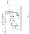
FIG. 3 depicts an example of amplifier ErrAmp2 during clock phase Φ2 according to one embodiment. In clock phase Φ2, switches S2 are closed and switches S1 are open, which isolate the input and output of amplifier ErrAmp2 from the input and output of amplifier ErrAmp1. In this case, amplifier ErrAmp2 may be in an open loop gain configuration. As discussed above, amplifier ErrAmp2 stores the offset error of amplifier ErrAmp2 on capacitors C2 during this clock phase.
Amplifier ErrAmp2 includes a first amplifier An1 and a second amplifier An2 that receive a first differential input and a second differential input, respectively. Both inputs of the differential input of amplifier An1 are coupled to battery 102. The offset error of amplifier An1 is shown as an offset error voltage Von1 at the input of one of the differential inputs.
To store the offset error of amplifier ErrAmp2, a feedback path from the output of amplifier ErrAmp2 to the differential input of amplifier An2 is used. In the feedback path, the output of amplifier ErrAmp2 (e.g., differential output VonullN and VonullP) is coupled to capacitors C2, which can store the offset error during clock phase Φ2. The offset error stored on capacitors C2 includes an inferred offset error voltage Von2 on one input of the differential input of amplifier An2 and the offset error voltage Von1.
In operation, the differential output vn1 of amplifier An1 and the differential output vn2 of amplifier An2 are added together to generate a differential output VonullN and VonullP. As will be discussed in more detail below, a common mode feedback circuit CMFB may shift the differential output calculation to a common mode voltage based on Vref. The differential output may be the combination of vn1+vn2, which reflect the offset errors Von1 and Von2. The outputs VonullN and VonullP are then stored on capacitors C2 during clock phase Φ2.
The following represents the calculation of the two control paths of the common mode and differential.
V ocm = A CMFB 1 + A CMFB V ref V onullP = V ocm + 1 2 ( v n 1 + v n 2 ) ( 1 ) V onullN = V ocm - 1 2 ( v n 1 + v n 2 ) ( 2 ) Δ V onull = V onullP - V onullN = ( v n 1 + v n 2 ) ( 3 ) v n 2 = A n 2 × ( v on 2 - Δ V onull ) ( 4 ) v n 1 = A n 1 × ( VBATT - VBATT + v on 1 ) ( 5 ) Δ V onull = V onullP - V onullN = ( v n 1 + v n 2 ) = A n 2 × ( v on 2 - Δ V onull ) + A n 1 × ( v on 1 ) = A n 2 1 + A n 2 ( v on 2 ) + A n 1 1 + A n 2 ( v on 1 ) ( 6 )
The voltage of the common mode amplifier Acm is based on the gain of amplifier Acm and a voltage Vref. Voltage Vref may be different from the voltage of the battery or rail, such as Vdd/2.
Equation 1 shows the calculation for output VonullP and equation 2 shows the calculation for output VonullN. In this case, output VonullP is the common mode output voltage Vocm plus half of the differential output of vn1 and vn2. Output VonullN is equal to the common mode voltage Vocm minus half of the differential output of vn1 and vn2. Equation 3 shows the calculation of the differential between outputs VonullN and VonullP and equations 4 and 5 show the calculation of the amplifier outputs of vn2 and vn1. As shown, equation 3 shows that the differential output ΔVonull is equal to the amplifier outputs vn1 and vn2 as the common mode voltage Vocm cancels. Output vn2 is equal to the gain of amplifier An2 and the offset error of amplifier An2 minus the differential output. Output vn1 is equal to the gain of amplifier An1 and the offset error of amplifier An1.
In equation 6, the differential output voltage ΔVonull may be determined based on equations 3, 4, and 5. Equation 6 shows that the differential output of amplifier ErrAmp2 is based on the offset errors Von1 and Von2 of amplifiers An1 and An2 and the gain of error amplifiers An1 and An2. These values are stored on capacitors C2 during clock phase Φ2. As will be discussed in the next figure, the values stored on capacitors C2 are used to cancel the offset errors Von1 and Von2 during the next clock phase Φ1.
FIG. 4 depicts an example of amplifiers ErrAmp1 (amplifiers A1 and A2) and ErrAmp2 (amplifiers An1 and An2) during clock phase Φ1 according to one embodiment. During clock phase Φ1, switches S1 are closed and switches S2 are open. This couples the differential output of ErrAmp2 to a differential input of ErrAmp1. This stores the offset error for amplifier ErrAmp1 on capacitors C1 via amplifier ErrAmp2. Further, the offset error of amplifier ErrAmp2 is canceled via the previous stored values on capacitors C2 in clock phase Φ2 so that the amplifier ErrAmp2 offset error does not affect the storing of the values on capacitors C1. The following will now discuss the offset compensation in more detail.
In amplifier ErrAmp1, the inputs of amplifier A1 are coupled to the output Vout of amplifier ErrAmp1 and the voltage of battery 102. The offset error of amplifier A1 is shown as an offset error voltage Vo1 on one of the inputs of amplifier A1. The differential input of amplifier A2 is coupled to the differential output of amplifier ErrAmp2. Also, the offset error of amplifier A2 is shown as an offset error voltage Vo2 on one of the inputs of amplifier A2.
In this clock phase, amplifier ErrAmp2 stores outputs VonullN and VonullP on capacitors C1. Equation 7 shows the differential voltage across capacitors C1:
Δ V onull 1 = V onull P 1 - V onull N 2 = A n 2 × [ v on 2 - A n 2 1 + A n 2 ( v on 2 ) - A n 1 1 + A n 2 ( v on 1 ) ] + A n 1 × ( v on 1 + VBATT - V out ) ( A n 2 × v on 2 ) - ( A n 2 × v on 2 ) - ( A n 1 × v on 1 ) + ( A n 1 × v on 1 ) + ( A n 1 × VBATT ) - ( A n 1 × V out ) A n 1 × ( VBATT - V out ) ( 7 )
As shown in equation 7, the differential output voltage of amplifier ErrAmp2 is equal to the gain of amplifier An1 times the difference between the battery voltage VBATT and the output voltage of amplifier ErrAmp1. The offset errors Von1 and Von2 of amplifiers An1 and An2 have been canceled in this case via the values stored on capacitors C2. That is, amplifier An2 cancels offset error Von2 and outputs offset error Von1 (e.g., Von1 times the gain of An2). This outputted offset error Von1 cancels the offset error from amplifier An1.
Now turning to amplifier ErrAmp1, the output Vout of amplifier ErrAmp1 substantially equals the battery voltage VBATT. Equation 8 shows the output of amplifier ErrAmp1 as follows:
V out = A 1 × ( VBATT - V out + v o 1 ) + A 2 × ( Δ V onuli 1 + v o 2 ) = A 1 × ( VBATT - V out + v o 1 ) + A 2 × [ ( A n 1 × ( VBATT - V out ) + v o 2 ] yields V out × [ 1 + A 1 + A 2 × A n 1 ] = [ VBATT × ( A 1 + A 2 × A n 1 ) ] + ( A 1 × v 01 ) + ( A 2 × v 0 2 ) yields V out × [ 1 + 1 A 1 + A 2 × A n 1 ] = VBATT + ( A 1 A 1 + A 2 × A n 1 × v 01 ) + ( A 2 A 1 + A 2 × A n 1 × v 02 ) ( 8 )
Because all open loop gain values are large (at least in the order of 1000), equation 8 can be approximated to:
V out VBATT + ( A 1 A 1 + A 2 × A n 1 × v 01 ) + ( A 2 A 1 + A 2 × A n 1 × v 02 ) VBATT
In the above, there is an effective cancellation of the offset errors Vo1 and Vo2, because the gain of amplifier An1 is large, which minimizes the values of Vo1 and Vo2 compared to the value of the battery voltage VBATT. Thus, the gain of amplifier An1 has been used to compensate for the offset errors of amplifiers An1 and An2.
In the above discussion of clock phase Φ2, amplifier ErrAmp2 was discussed. In this clock phase, amplifier ErrAmp1 also operates in an open loop gain configuration where the values stored on capacitors C1 are used to compensate for the offset errors of amplifiers A1 and A2. FIG. 5 depicts an example of amplifier ErrAmp1 in clock phase Φ2 according to one embodiment. The inputs of amplifier A1 are coupled to the output Vout of amplifier ErrAmp1 and to the battery voltage VBATT. The offset error voltage Vo1 is also shown at an input of amplifier A1. Also, the inputs of amplifier A2 are coupled to capacitors C1. The offset error voltage Vo2 is also shown at an input of amplifier A2.
As shown in equation 10 below, capacitors C1 hold the differential voltage ΔVonull1, which is based on the gain of amplifiers A1 and A2 and the offset errors of amplifiers A1 and A2 of Vo1 and Vo2. In equation 7 above, the differential output voltage of amplifier ErrAmp2 is equal to the gain of Amplifier An1 times the difference of VBATT and Vout. In this case, the values stored on capacitors C1 are a function of the gain of amplifiers A1 and A2 and the offset errors Vo1 and Vo2. Equation 10 summarizes these values:
Δ V onull 1 = - ( 1 1 A n 1 + A 2 A 1 × v 01 ) - ( 1 A 1 A 2 × A n 1 + 1 × v 02 ) - A 1 A 2 × v 01 - v 02 ( 10 )
The following shows the cancellation of the offset errors of amplifiers A1 and A2 based on the values stored in capacitors C1. That is, the offset errors stored on capacitors C1 compensate for the offset error of amplifiers Vo1 and Vo2 during this clock phase. Equation 11 represents the determination of the output voltage Vout of ErrAmp1, which shows the cancellation of offset errors Vo1 and Vo2 as follows:
V out = A 1 × ( VBATT - V out + v o 1 ) + A 2 × ( Δ V onull 1 + v o 2 ) = A 1 × ( VBATT - V out + v o 1 ) + A 2 × [ - A 1 A 2 × v 01 - v 02 + v o 2 ] V out = A 1 × ( VBATT - V out + v o 1 ) + A 2 × ( Δ V onull 1 + v o 2 ) = A 1 × ( VBATT - V out + v o 1 ) + A 2 × [ - A 1 A 2 × v 01 - v 02 + v o 2 ] = A 1 × ( VBATT - V out ) + ( A 1 × v o 1 - A 1 × v o 1 ) yields V out × [ 1 + A 1 ] A 1 × VBATT yields V out = A 1 1 + A 1 × VBATT yields V out VBATT ( 11 )
As seen in equation 11, the offset errors Vo1 and Vo2 are cancelled and the output voltage Vout of amplifier ErrAmp1 approximately equals the battery voltage VBATT, Vout≈VBATT. In this case, as seen in equation 10, the values stored on capacitors C1 include offset errors Vo1 and Vo2. The offset error Vo2 stored on capacitor C1 cancels the offset error Vo2 of amplifier A2. Then, amplifier A2 outputs offset error Vo1 amplified by the gain A2 of amplifier A2. Also, amplifier A1 outputs offset error Vo1 amplified by the gain A1 of amplifier A1. The outputs of amplifiers A1 and A2 are of the opposite polarity and thus cancel offset error Vo1 when combined. Accordingly, the offset errors of Vo1 and Vo2 are cancelled in clock phase Φ2 and output voltage Vout substantially equals the battery voltage VBATT.
Different implementations of amplifiers ErrAmp1 and ErrAmp2 may be appreciated. FIGS. 6 and 7 show examples of implementations of ErrAmp1 and ErrAmp2, respectively. However, it will be understood that other implementations may be appreciated.
In FIG. 6, differential amplifiers A1 and A2 are shown as a differential pair of transistors MA1 and a differential pair of transistors MA2. Amplifiers A1 and A2 are coupled to a shared output stage 602. Shared output stage 602 provides a resistor gain that converts a current output of differential amplifiers A1 and A2 into a voltage output. Different variations of shared output stage 602 may be appreciated.
In FIG. 7, differential amplifiers An1 and An2 are shown as a differential pair of transistors MAN2 and a differential pair of transistors MAN1, respectively. The output of amplifiers An1 and An2 are coupled to a shared output stage 702. Shared output stage 702 also converts a current output of amplifiers An1 and An2 to a voltage, but the output of shared output stage 702 is a differential output Out− and Out+. Also, a common mode feedback circuit 704 is coupled to the differential output and maintains an average value of the differential output at a fixed level based on a voltage Vref, which may be at a different level than the rail voltage, such as ½(Vdd). Using common mode feedback circuit 704, the differential voltage measurement is moved away from the rail voltage or battery voltage VBATT. For example, if the differential voltage measurement is close to the rail, then it might be hard to measure the differential voltage accurately. Thus, setting the common mode differential output voltage to a value, such as ½ of the rail voltage, makes calculating the offset at the average value more accurate. That is, outputs Out+ and Out− are both set at a common mode voltage. Then, the differential of outputs Out+ and Out− can be calculated based on that common mode value that is different from the rail voltage. The common mode voltage drops out while the differential voltage is output on outputs Out+ and Out−. Using the common mode voltage at around half the battery voltage VBATT may simplify the output stage 702.
Although a differential output of amplifier ErrAmp2 was discussed above, a single output may be used. In this case, the differential output voltage at the output of amplifier ErrAmp2 is not performed at the common mode level. This may decrease the accuracy, but offset error compensation is still performed as described above. FIG. 8 shows an example of a battery monitoring system 800 using a single output of amplifier ErrAmp2 according to one embodiment. As shown, a single output of amplifier ErrAmp2 is coupled to amplifier ErrAmp1. Also, the single output of amplifier ErrAmp2 is coupled to an input of amplifier ErrAmp2 in a feedback configuration. Another input of amplifier ErrAmp2 and another input of amplifier ErrAmp1 are coupled to a voltage Vref, which may be a voltage different from the rail voltage.
In clock phase Φ2, the voltage stored across capacitors C2 includes the offset errors Von1 and Von2. In clock phase Φ1, these stored offset errors compensate for the offset errors of amplifier ErrAmp2. Also, in clock phase Φ1, Vout VBATT due to the gain of amplifier An2 (not shown) of amplifier ErrAmp2 substantially canceling the offset errors of amplifier ErrAmp1. Further, in clock phase Φ2, the offset error stored on capacitors C1 cancels the error of amplifier ErrAmp1.
FIG. 9 depicts a simplified flowchart 900 of a method for compensating for offset error according to one embodiment. At 902, during a first phase, amplifier ErrAm2 stores a first offset error of amplifier ErrAmp1 on capacitors C1 for use in compensating for the offset error of amplifier ErrAmp1 during a second phase. At 904, during the second phase, amplifier ErrAmp2 stores an offset error of amplifier ErrAmp2 on capacitors C2 for use in compensating for the offset error of amplifier ErrAmp2 during a subsequent first phase. At 906, during the second phase, amplifier ErrAmp1 controls control transistor MC to control a replica current generated by the replica device. During this phase, the first offset error is compensated for using the first offset error stored during the first phase. At 908, during a subsequent first phase, amplifier ErrAmp1 controls control transistor MC to control the replica current where a gain of the second amplifier is used to compensate for the offset error of amplifier ErrAmp1 and the offset error of amplifier ErrAmp2 is compensated for using the offset error of amplifier ErrAmp2 stored on capacitors C2 during the second phase.
Temperature Variation Offset
As discussed above, sensing resistor R1 may be located on chip and thus may be sensitive to temperature variations of the chip. FIG. 10 shows an example implementation of resistor R1 to compensate for temperature variations according to one embodiment. The temperature variations may be compensated for during the current voltage conversion using two types of resistors. The first type of resistor R is a poly resistor with P+ doping having a negative temperature coefficient. The second type of resistors rsp are silicided and having a positive temperature coefficient. The opposite temperature coefficients can be used to compensate for temperature variations.
As shown, the size of resistor rsp (e.g., rsp 1, rsp 2, rsp 3, . . . rsp N) can be adjusted via taps 1002. Different tap settings may be used to adjust for the temperature variation by opening or closing different taps to couple various resistors rsp to the replica current. The size of resistors rsp may then compensate for the temperature variation. For example, the size of resistors rsp will determine the final slope of the resistance with respect to temperatures.
FIG. 11 depicts an example of the temperature correction using resistor rsp1 according to one embodiment. Resistor RSP in FIG. 10 represents the combination of resistors rsp1-rspN that are coupled to the replica current based on the tap settings. In this case, Vout may be determined as follows:
Vout≈½(R+½rsp).
As shown, the output voltage Vout across sensing resistor R1 is equal to the resistance of R that is compensated by the resistance of resistor rsp. Although internal resistors are discussed as being used, particular embodiments may also use external resistors that are off-chip and thus do not need temperature compensation.
The above description illustrates various embodiments of the present disclosure along with examples of how aspects of the particular embodiments may be implemented. The above examples should not be deemed to be the only embodiments, and are presented to illustrate the flexibility and advantages of the particular embodiments as defined by the following claims. Based on the above disclosure and the following claims, other arrangements, embodiments, implementations and equivalents may be employed without departing from the scope of the present disclosure as defined by the claims.

Claims (20)

What is claimed is:
1. A circuit comprising:
a first amplifier comprising a first differential input, a second differential input, and an output, the first differential input coupled to a replica device and a voltage of a battery and the output coupled to a control device, the replica device configured to generate a replica current of a current flowing through the battery where the first amplifier controls the control device to control the replica current; and
a second amplifier comprising a third differential input, a fourth differential input, and an output, wherein the second amplifier is configured to compensate for a first offset error of the first amplifier and a second offset error of the second amplifier based on selectively coupling the third differential input to the output of the first amplifier during a first phase, selectively coupling the output of the second amplifier to the second differential input during the first phase, and selectively coupling the output of the second amplifier to the fourth differential input during a second phase.
2. The circuit of claim 1, wherein during the second phase, the second amplifier stores the second offset error of the second amplifier on a first set of storage elements coupled to the fourth differential input of the second amplifier for use in compensating for the second offset error of the second amplifier during the first phase.
3. The circuit of claim 2, wherein during the first phase, the second amplifier stores the first offset error of the first amplifier on a second set of storage elements coupled to the second differential input of the first amplifier for use in compensating for the first offset error of the first amplifier during a subsequent second phase.
4. The circuit of claim 3, wherein a gain of the second amplifier is used to compensate for the first offset error during the first phase.
5. The circuit of claim 1, wherein the second amplifier includes a third amplifier including the third differential input and a fourth amplifier including the fourth differential input, and wherein during the second phase:
a first input and a second input of the third differential input are coupled to the voltage of the battery, wherein the third amplifier includes a third amplifier offset error of the second offset error, and
a first input of the fourth differential input is coupled to the output of the second amplifier, wherein the fourth amplifier includes a fourth amplifier offset error of the second offset error.
6. The circuit of claim 5, wherein:
a first set of storage elements are coupled to the fourth differential input and the output of the second amplifier during the second phase, and
the first set of storage elements is configured to store the third amplifier offset error and the fourth amplifier offset error during the second phase.
7. The circuit of claim 6, wherein:
the third amplifier offset error and the fourth amplifier offset error stored during the second phase are used to compensate for the third amplifier offset error and the fourth amplifier offset error during a subsequent first phase.
8. The circuit of claim 5, wherein:
the first input of the fourth differential input is coupled to a first differential output of the second amplifier, and
a second input of the fourth differential input is coupled to a second differential output of the second amplifier.
9. The circuit of claim 5, wherein the first amplifier includes a fifth amplifier including the first differential input and a sixth amplifier including the second differential input, and wherein during the first phase:
a first input of the first differential input is coupled to the output of the first amplifier and a second input of the first differential input is coupled to the voltage of the battery, the fifth amplifier including a fifth amplifier offset error of the first offset error, and
a first input of the second differential input is coupled to the output of the second amplifier, the sixth amplifier including a sixth amplifier offset error of the first offset error.
10. The circuit of claim 9, wherein:
a gain of the second amplifier is used to compensate for the fifth amplifier offset error and the sixth amplifier offset error during the first phase.
11. The circuit of claim 10, wherein:
the second set of storage elements are coupled to the second differential input and the output of the second amplifier during the first phase, and
the second set of storage elements is configured to store the fifth amplifier offset error and the sixth amplifier offset error during the first phase.
12. The circuit of claim 11, wherein:
the fifth amplifier offset error and the sixth amplifier offset error stored during the second phase are used to compensate for the fifth amplifier offset error and the sixth amplifier offset error during a subsequent second phase.
13. The circuit of claim 9, wherein:
the first input of the second differential input is coupled to a first differential output of the second amplifier, and
a second input of the second differential input is coupled to a second differential output of the second amplifier.
14. The circuit of claim 1, wherein the output of the second amplifier is a differential output, the circuit further comprising:
a common mode feedback circuit coupled to the differential output and configured to maintain a common mode portion of the differential output at a fixed value different from the voltage of the battery.
15. The circuit of claim 1, further comprising:
a resistor configured to receive the replica current, wherein a voltage across the resistor is sensed to monitor the voltage across the battery.
16. The circuit of claim 15, wherein the resistor is configured to compensate for temperature changes.
17. The circuit of claim 16, wherein:
the resistor comprises a first set of resistors and a second set of resistors,
the first set of resistors have a first temperature coefficient and a second set of resistors have a second temperature coefficient that is opposite of the first temperature coefficient,
the first set of resistors are selectively coupled to a plurality of taps, and
taps in the plurality of taps selective connect resistors in the first set of resistors to compensate for temperature variations.
18. A method comprising:
during a first phase, storing, by a second amplifier, a first offset error of a first amplifier on a first set of storage elements coupled to a differential input of the first amplifier for use in compensating for the first offset error of the first amplifier during a second phase;
during the second phase, storing, by the second amplifier, a second offset error of the second amplifier on a second set of storage elements coupled to a differential input of the second amplifier for use in compensating for the second offset error of the second amplifier during a subsequent first phase;
during the second phase, controlling, by the first amplifier, a control device to control a replica current generated by the replica device, the replica current being a replica of a current flowing through the battery, wherein the first offset error is compensated for using the first offset error stored during the first phase; and
during the subsequent first phase, controlling, by the first amplifier, the control device to control the replica current, wherein a gain of the second amplifier is used to compensate for the first offset error and the second offset error is compensated for using the second offset error stored during the second phase.
19. The method of claim 18, further comprising maintaining a common mode portion of a differential output of the second amplifier at a fixed value different from a voltage of the battery.
20. The method of claim 18, further comprising coupling a resistor configured to receive the replica current to the control device, wherein a voltage across the resistor is sensed to monitor a voltage across the battery and the resistor is configured to compensate for temperature variations.
US14/149,739 2014-01-07 2014-01-07 Compensation technique for amplifiers in a current sensing circuit for a battery Active 2034-08-09 US9217780B2 (en)

Priority Applications (6)

Application Number Priority Date Filing Date Title
US14/149,739 US9217780B2 (en) 2014-01-07 2014-01-07 Compensation technique for amplifiers in a current sensing circuit for a battery
EP15701441.6A EP3092501B1 (en) 2014-01-07 2015-01-07 Compensation technique for amplifiers in a current sensing circuit for a battery
KR1020167021298A KR101740581B1 (en) 2014-01-07 2015-01-07 Compensation technique for amplifiers in a current sensing circuit for a battery
JP2016542735A JP6602766B2 (en) 2014-01-07 2015-01-07 Compensation techniques for amplifiers in battery current sensing circuits.
PCT/US2015/010529 WO2015105915A1 (en) 2014-01-07 2015-01-07 Compensation technique for amplifiers in a current sensing circuit for a battery
CN201580003828.5A CN105899958B (en) 2014-01-07 2015-01-07 For the compensation technique for the amplifier in the current sensing circuit of battery

Applications Claiming Priority (1)

Application Number Priority Date Filing Date Title
US14/149,739 US9217780B2 (en) 2014-01-07 2014-01-07 Compensation technique for amplifiers in a current sensing circuit for a battery

Publications (2)

Publication Number Publication Date
US20150192642A1 US20150192642A1 (en) 2015-07-09
US9217780B2 true US9217780B2 (en) 2015-12-22

Family

ID=52424124

Family Applications (1)

Application Number Title Priority Date Filing Date
US14/149,739 Active 2034-08-09 US9217780B2 (en) 2014-01-07 2014-01-07 Compensation technique for amplifiers in a current sensing circuit for a battery

Country Status (6)

Country Link
US (1) US9217780B2 (en)
EP (1) EP3092501B1 (en)
JP (1) JP6602766B2 (en)
KR (1) KR101740581B1 (en)
CN (1) CN105899958B (en)
WO (1) WO2015105915A1 (en)

Cited By (2)

* Cited by examiner, † Cited by third party
Publication number Priority date Publication date Assignee Title
US11422168B2 (en) 2020-09-16 2022-08-23 Nxp Usa, Inc. On-chip, low-voltage, current sensing circuit
US12068743B2 (en) * 2022-02-21 2024-08-20 Fuji Electric Co., Ltd. Semiconductor device

Families Citing this family (3)

* Cited by examiner, † Cited by third party
Publication number Priority date Publication date Assignee Title
JP6338807B1 (en) * 2017-11-13 2018-06-06 三菱電機株式会社 Class AB amplifier and operational amplifier
US20240056044A1 (en) * 2021-02-04 2024-02-15 Semiconductor Components Industries, Llc Precision operational amplifier using floating input stage
EP4170906B1 (en) 2021-10-20 2024-06-19 STMicroelectronics S.r.l. Current sensing in switched electronic devices

Citations (15)

* Cited by examiner, † Cited by third party
Publication number Priority date Publication date Assignee Title
US5498984A (en) 1994-09-30 1996-03-12 Maxim Integrated Products High side, current sense amplifier using a symmetric amplifier
US5945853A (en) 1997-04-24 1999-08-31 Sanyo Electric Co., Ltd. Current sensing circuit with automatic offset compensation
US20020180418A1 (en) 2001-05-30 2002-12-05 Texas Instruments Incorporated Current sense amplifier and method
US20090137211A1 (en) * 2007-11-28 2009-05-28 Motorola, Inc. Method and apparatus for reconfigurable frequency generation
WO2012117275A2 (en) 2011-03-01 2012-09-07 Sendyne Corp. Current sensor
US20120249243A1 (en) 2011-03-30 2012-10-04 Microchip Technology Incorporated Low switching error, small capacitors, auto-zero offset buffer amplifier
US20130033309A1 (en) 2011-08-01 2013-02-07 Jung-Hyun Choi Poly silicon resistor, reference voltage circuit comprising the same, and manufacturing method of poly silicon resistor
US20130120027A1 (en) * 2010-09-15 2013-05-16 Fumihiro Inoue Differential circuit
US20130134988A1 (en) * 2011-11-30 2013-05-30 Standard Microsystems Corporation Method and system for high gain auto-zeroing arrangement for electronic circuits
US8476890B2 (en) 2008-02-05 2013-07-02 Qualcomm Incorporated Circuits and methods for controlling a switching regulator based on a derived input current
US8525497B2 (en) 2010-02-04 2013-09-03 Rickhtek Tecnology Corp. Using offset cancellation circuit to mitigate beat-frequency oscillation of phase currents in a multiphase interleaved voltage regulator
US8901891B2 (en) * 2009-02-25 2014-12-02 Panasonic Corporation Voltage polarity determination circuit and charge amount measurement circuit
US20150022241A1 (en) * 2012-03-22 2015-01-22 Seiko Instruments Inc. Sensor device
US20150040687A1 (en) * 2012-04-27 2015-02-12 Seiko Instruments Inc. Sensor device
US20150145588A1 (en) * 2013-11-22 2015-05-28 Analog Devices, Inc. Bi-directional current sensor

Family Cites Families (12)

* Cited by examiner, † Cited by third party
Publication number Priority date Publication date Assignee Title
NL8503394A (en) * 1985-12-10 1987-07-01 Philips Nv CURRENT SCREENING FOR A POWER SEMICONDUCTOR DEVICE, PARTICULARLY INTEGRATED INTELLIGENT POWER SEMICONDUCTOR SWITCH FOR PARTICULAR AUTOMOTIVE APPLICATIONS.
JP3102020B2 (en) * 1990-08-15 2000-10-23 日本電気株式会社 Operational amplifier circuit
US5495154A (en) * 1993-04-29 1996-02-27 Sgs-Thomson Microelectronics, Inc. Method and apparatus for Kelvin current sensing in a multi-phase driver for a polyphase DC motor
DE19706946C2 (en) * 1997-02-21 2000-06-21 Daimler Chrysler Ag Battier monitoring unit
JP2000004129A (en) * 1998-06-17 2000-01-07 Toshiba Ave Co Ltd Cmos analog circuit
US6914425B2 (en) * 2003-04-29 2005-07-05 Teradyne, Inc. Measurement circuit with improved accuracy
US7382183B2 (en) * 2006-07-18 2008-06-03 Microchip Technology Incorporated Minimizing switching noise and its effects in auto-zeroed amplifiers
JP2009081749A (en) * 2007-09-27 2009-04-16 Hitachi Ltd Low offset input circuit
JP4976323B2 (en) * 2008-03-06 2012-07-18 株式会社リコー Charge control circuit
DE102008032556B3 (en) * 2008-07-10 2009-09-10 Infineon Technologies Austria Ag Power circuit breaker e.g. high side circuit breaker, has coupling transistors for dividing signal current into internal and external signal currents, and measuring device for determining whether evaluation device is coupled to breaker
WO2010044012A1 (en) * 2008-10-15 2010-04-22 Nxp B.V. Low-voltage self-calibrated cmos peak detector
WO2011145970A1 (en) * 2010-05-21 2011-11-24 Freescale Semiconductor, Inc. Power switching apparatus and method for improving current sense accuracy

Patent Citations (16)

* Cited by examiner, † Cited by third party
Publication number Priority date Publication date Assignee Title
US5498984A (en) 1994-09-30 1996-03-12 Maxim Integrated Products High side, current sense amplifier using a symmetric amplifier
US5945853A (en) 1997-04-24 1999-08-31 Sanyo Electric Co., Ltd. Current sensing circuit with automatic offset compensation
US20020180418A1 (en) 2001-05-30 2002-12-05 Texas Instruments Incorporated Current sense amplifier and method
US20090137211A1 (en) * 2007-11-28 2009-05-28 Motorola, Inc. Method and apparatus for reconfigurable frequency generation
US8476890B2 (en) 2008-02-05 2013-07-02 Qualcomm Incorporated Circuits and methods for controlling a switching regulator based on a derived input current
US8901891B2 (en) * 2009-02-25 2014-12-02 Panasonic Corporation Voltage polarity determination circuit and charge amount measurement circuit
US8525497B2 (en) 2010-02-04 2013-09-03 Rickhtek Tecnology Corp. Using offset cancellation circuit to mitigate beat-frequency oscillation of phase currents in a multiphase interleaved voltage regulator
US20130120027A1 (en) * 2010-09-15 2013-05-16 Fumihiro Inoue Differential circuit
US20130009655A1 (en) * 2011-03-01 2013-01-10 Sendyne Corporation Current sensor
WO2012117275A2 (en) 2011-03-01 2012-09-07 Sendyne Corp. Current sensor
US20120249243A1 (en) 2011-03-30 2012-10-04 Microchip Technology Incorporated Low switching error, small capacitors, auto-zero offset buffer amplifier
US20130033309A1 (en) 2011-08-01 2013-02-07 Jung-Hyun Choi Poly silicon resistor, reference voltage circuit comprising the same, and manufacturing method of poly silicon resistor
US20130134988A1 (en) * 2011-11-30 2013-05-30 Standard Microsystems Corporation Method and system for high gain auto-zeroing arrangement for electronic circuits
US20150022241A1 (en) * 2012-03-22 2015-01-22 Seiko Instruments Inc. Sensor device
US20150040687A1 (en) * 2012-04-27 2015-02-12 Seiko Instruments Inc. Sensor device
US20150145588A1 (en) * 2013-11-22 2015-05-28 Analog Devices, Inc. Bi-directional current sensor

Non-Patent Citations (1)

* Cited by examiner, † Cited by third party
Title
International Search Report and Written Opinion-PCT/US2015/010529-ISA/EPO-Apr. 2, 2015.

Cited By (2)

* Cited by examiner, † Cited by third party
Publication number Priority date Publication date Assignee Title
US11422168B2 (en) 2020-09-16 2022-08-23 Nxp Usa, Inc. On-chip, low-voltage, current sensing circuit
US12068743B2 (en) * 2022-02-21 2024-08-20 Fuji Electric Co., Ltd. Semiconductor device

Also Published As

Publication number Publication date
CN105899958B (en) 2018-11-23
EP3092501A1 (en) 2016-11-16
KR20160098518A (en) 2016-08-18
CN105899958A (en) 2016-08-24
US20150192642A1 (en) 2015-07-09
KR101740581B1 (en) 2017-05-26
EP3092501B1 (en) 2017-09-13
JP2017503416A (en) 2017-01-26
JP6602766B2 (en) 2019-11-06
WO2015105915A1 (en) 2015-07-16

Similar Documents

Publication Publication Date Title
US9217780B2 (en) Compensation technique for amplifiers in a current sensing circuit for a battery
US9444414B2 (en) Current sense circuit using a single opamp having DC offset auto-zeroing
CN110366820B (en) Self-heating compensation circuit of power amplifier
US8796998B2 (en) Bidirectional current sense
US10523166B2 (en) Differential amplifier with modified common mode rejection, and to a circuit with an improved common mode rejection ratio
US9671438B2 (en) High-current sensing scheme using drain-source voltage
US7656233B2 (en) Apparatus for high power amplifier in wireless communication system
US9217777B2 (en) Current sense circuit for measuring a charge level of a battery
US8717033B2 (en) Integrated MOSFET current sensing for fuel-gauging
WO2007007765A1 (en) Current-voltage conversion circuit and power consumption detection circuit and electronic device using the same
US9182428B2 (en) Switched capacitance voltage differential sensing circuit with near infinite input impedance
JPH1169635A (en) Charge and discharge control circuit with detecting function of charging and discharging currents / and rechargeable power supply
CN107003268B (en) Control circuit for use with a sensor and measurement system comprising the control circuit
CN104458034A (en) Temperature measuring method and device
IT9068063A1 (en) CIRCUIT FOR THE TREATMENT OF THE SIGNAL SUPPLIED BY AN OXYGEN SENSOR OF THE ZIRCONIUM TYPE.
US6400225B1 (en) Differential difference amplifier for amplifying small signals close to zero volts
US9568518B2 (en) Power measuring device with internal calibration of diode detectors
US20100045383A1 (en) Variable gain circuit
US7126423B1 (en) Differential difference amplifier for amplifying small signals close to zero volts
CN114152797A (en) Current sensor capable of automatically adjusting offset voltage
US10679938B2 (en) Power transistor coupled to multiple sense transistors
Galliana et al. High accuracy transportable selectable-Value High Dc Voltage Standard

Legal Events

Date Code Title Description
AS Assignment

Owner name: QUALCOMM INCORPORATED, CALIFORNIA

Free format text: ASSIGNMENT OF ASSIGNORS INTEREST;ASSIGNOR:BASHAR, ANIRUDDHA;REEL/FRAME:033590/0458

Effective date: 20140121

FEPP Fee payment procedure

Free format text: PAYOR NUMBER ASSIGNED (ORIGINAL EVENT CODE: ASPN); ENTITY STATUS OF PATENT OWNER: LARGE ENTITY

STCF Information on status: patent grant

Free format text: PATENTED CASE

MAFP Maintenance fee payment

Free format text: PAYMENT OF MAINTENANCE FEE, 4TH YEAR, LARGE ENTITY (ORIGINAL EVENT CODE: M1551); ENTITY STATUS OF PATENT OWNER: LARGE ENTITY

Year of fee payment: 4

MAFP Maintenance fee payment

Free format text: PAYMENT OF MAINTENANCE FEE, 8TH YEAR, LARGE ENTITY (ORIGINAL EVENT CODE: M1552); ENTITY STATUS OF PATENT OWNER: LARGE ENTITY

Year of fee payment: 8