EP3050122B1 - Metallization of solar cells using metal foils - Google Patents
Metallization of solar cells using metal foils Download PDFInfo
- Publication number
- EP3050122B1 EP3050122B1 EP14847743.3A EP14847743A EP3050122B1 EP 3050122 B1 EP3050122 B1 EP 3050122B1 EP 14847743 A EP14847743 A EP 14847743A EP 3050122 B1 EP3050122 B1 EP 3050122B1
- Authority
- EP
- European Patent Office
- Prior art keywords
- metal
- solar cell
- metal foil
- metal layer
- cell structure
- Prior art date
- Legal status (The legal status is an assumption and is not a legal conclusion. Google has not performed a legal analysis and makes no representation as to the accuracy of the status listed.)
- Active
Links
- 229910052751 metal Inorganic materials 0.000 title claims description 215
- 239000002184 metal Substances 0.000 title claims description 215
- 239000011888 foil Substances 0.000 title claims description 108
- 238000001465 metallisation Methods 0.000 title description 4
- 238000000034 method Methods 0.000 claims description 44
- 125000006850 spacer group Chemical group 0.000 claims description 41
- 238000000059 patterning Methods 0.000 claims description 18
- 238000004519 manufacturing process Methods 0.000 claims description 12
- 238000003466 welding Methods 0.000 claims description 9
- 238000000151 deposition Methods 0.000 claims description 8
- 230000008021 deposition Effects 0.000 claims description 7
- XAGFODPZIPBFFR-UHFFFAOYSA-N aluminium Chemical compound [Al] XAGFODPZIPBFFR-UHFFFAOYSA-N 0.000 claims description 6
- 229910052782 aluminium Inorganic materials 0.000 claims description 5
- 238000000608 laser ablation Methods 0.000 description 14
- 239000000758 substrate Substances 0.000 description 6
- 230000005855 radiation Effects 0.000 description 4
- 238000005530 etching Methods 0.000 description 3
- 229910021420 polycrystalline silicon Inorganic materials 0.000 description 3
- 229920005591 polysilicon Polymers 0.000 description 3
- 238000002679 ablation Methods 0.000 description 2
- 238000010586 diagram Methods 0.000 description 2
- 239000002019 doping agent Substances 0.000 description 2
- 230000000873 masking effect Effects 0.000 description 2
- 239000000463 material Substances 0.000 description 2
- 238000007650 screen-printing Methods 0.000 description 2
- 238000004528 spin coating Methods 0.000 description 2
- 239000004642 Polyimide Substances 0.000 description 1
- GWEVSGVZZGPLCZ-UHFFFAOYSA-N Titan oxide Chemical compound O=[Ti]=O GWEVSGVZZGPLCZ-UHFFFAOYSA-N 0.000 description 1
- 239000006096 absorbing agent Substances 0.000 description 1
- 238000010521 absorption reaction Methods 0.000 description 1
- 230000015572 biosynthetic process Effects 0.000 description 1
- 238000005229 chemical vapour deposition Methods 0.000 description 1
- 239000011248 coating agent Substances 0.000 description 1
- 238000000576 coating method Methods 0.000 description 1
- 239000003989 dielectric material Substances 0.000 description 1
- 238000011065 in-situ storage Methods 0.000 description 1
- 229910021421 monocrystalline silicon Inorganic materials 0.000 description 1
- 230000003287 optical effect Effects 0.000 description 1
- 238000007747 plating Methods 0.000 description 1
- 229920001721 polyimide Polymers 0.000 description 1
- 238000003825 pressing Methods 0.000 description 1
- 238000000926 separation method Methods 0.000 description 1
- 238000004544 sputter deposition Methods 0.000 description 1
- 239000000126 substance Substances 0.000 description 1
- OGIDPMRJRNCKJF-UHFFFAOYSA-N titanium oxide Inorganic materials [Ti]=O OGIDPMRJRNCKJF-UHFFFAOYSA-N 0.000 description 1
Images


Classifications
-
- H—ELECTRICITY
- H01—ELECTRIC ELEMENTS
- H01L—SEMICONDUCTOR DEVICES NOT COVERED BY CLASS H10
- H01L31/00—Semiconductor devices sensitive to infrared radiation, light, electromagnetic radiation of shorter wavelength or corpuscular radiation and specially adapted either for the conversion of the energy of such radiation into electrical energy or for the control of electrical energy by such radiation; Processes or apparatus specially adapted for the manufacture or treatment thereof or of parts thereof; Details thereof
- H01L31/02—Details
- H01L31/0224—Electrodes
- H01L31/022408—Electrodes for devices characterised by at least one potential jump barrier or surface barrier
- H01L31/022425—Electrodes for devices characterised by at least one potential jump barrier or surface barrier for solar cells
- H01L31/022441—Electrode arrangements specially adapted for back-contact solar cells
-
- H—ELECTRICITY
- H01—ELECTRIC ELEMENTS
- H01L—SEMICONDUCTOR DEVICES NOT COVERED BY CLASS H10
- H01L31/00—Semiconductor devices sensitive to infrared radiation, light, electromagnetic radiation of shorter wavelength or corpuscular radiation and specially adapted either for the conversion of the energy of such radiation into electrical energy or for the control of electrical energy by such radiation; Processes or apparatus specially adapted for the manufacture or treatment thereof or of parts thereof; Details thereof
- H01L31/02—Details
- H01L31/0236—Special surface textures
- H01L31/02366—Special surface textures of the substrate or of a layer on the substrate, e.g. textured ITO/glass substrate or superstrate, textured polymer layer on glass substrate
-
- H—ELECTRICITY
- H01—ELECTRIC ELEMENTS
- H01L—SEMICONDUCTOR DEVICES NOT COVERED BY CLASS H10
- H01L31/00—Semiconductor devices sensitive to infrared radiation, light, electromagnetic radiation of shorter wavelength or corpuscular radiation and specially adapted either for the conversion of the energy of such radiation into electrical energy or for the control of electrical energy by such radiation; Processes or apparatus specially adapted for the manufacture or treatment thereof or of parts thereof; Details thereof
- H01L31/04—Semiconductor devices sensitive to infrared radiation, light, electromagnetic radiation of shorter wavelength or corpuscular radiation and specially adapted either for the conversion of the energy of such radiation into electrical energy or for the control of electrical energy by such radiation; Processes or apparatus specially adapted for the manufacture or treatment thereof or of parts thereof; Details thereof adapted as photovoltaic [PV] conversion devices
- H01L31/06—Semiconductor devices sensitive to infrared radiation, light, electromagnetic radiation of shorter wavelength or corpuscular radiation and specially adapted either for the conversion of the energy of such radiation into electrical energy or for the control of electrical energy by such radiation; Processes or apparatus specially adapted for the manufacture or treatment thereof or of parts thereof; Details thereof adapted as photovoltaic [PV] conversion devices characterised by potential barriers
- H01L31/068—Semiconductor devices sensitive to infrared radiation, light, electromagnetic radiation of shorter wavelength or corpuscular radiation and specially adapted either for the conversion of the energy of such radiation into electrical energy or for the control of electrical energy by such radiation; Processes or apparatus specially adapted for the manufacture or treatment thereof or of parts thereof; Details thereof adapted as photovoltaic [PV] conversion devices characterised by potential barriers the potential barriers being only of the PN homojunction type, e.g. bulk silicon PN homojunction solar cells or thin film polycrystalline silicon PN homojunction solar cells
- H01L31/0682—Semiconductor devices sensitive to infrared radiation, light, electromagnetic radiation of shorter wavelength or corpuscular radiation and specially adapted either for the conversion of the energy of such radiation into electrical energy or for the control of electrical energy by such radiation; Processes or apparatus specially adapted for the manufacture or treatment thereof or of parts thereof; Details thereof adapted as photovoltaic [PV] conversion devices characterised by potential barriers the potential barriers being only of the PN homojunction type, e.g. bulk silicon PN homojunction solar cells or thin film polycrystalline silicon PN homojunction solar cells back-junction, i.e. rearside emitter, solar cells, e.g. interdigitated base-emitter regions back-junction cells
-
- Y—GENERAL TAGGING OF NEW TECHNOLOGICAL DEVELOPMENTS; GENERAL TAGGING OF CROSS-SECTIONAL TECHNOLOGIES SPANNING OVER SEVERAL SECTIONS OF THE IPC; TECHNICAL SUBJECTS COVERED BY FORMER USPC CROSS-REFERENCE ART COLLECTIONS [XRACs] AND DIGESTS
- Y02—TECHNOLOGIES OR APPLICATIONS FOR MITIGATION OR ADAPTATION AGAINST CLIMATE CHANGE
- Y02E—REDUCTION OF GREENHOUSE GAS [GHG] EMISSIONS, RELATED TO ENERGY GENERATION, TRANSMISSION OR DISTRIBUTION
- Y02E10/00—Energy generation through renewable energy sources
- Y02E10/50—Photovoltaic [PV] energy
- Y02E10/547—Monocrystalline silicon PV cells
Definitions
- Embodiments of the subject matter described herein relate generally to solar cells. More particularly, embodiments of the subject matter relate to solar cell fabrication processes and structures.
- Solar cells are well known devices for converting solar radiation to electrical energy.
- a solar cell has a front side that faces the sun during normal operation to collect solar radiation and a backside opposite the front side. Solar radiation impinging on the solar cell creates electrical charges that may be harnessed to power an external electrical circuit, such as a load.
- the external electrical circuit may receive electrical current from the solar cell by way of metal fingers that are connected to doped regions of the solar cell.
- US 2011/053312 A1 relates to a method for a contact separation of electrically-conducting layers on a back contact of a solar cell.
- US 2010/051085 A1 relates to a back contact solar cell module.
- a dielectric spacer is formed on a surface of a solar cell structure.
- a metal layer is formed on the dielectric spacer and on the surface of the solar cell structure that is exposed by the dielectric spacer.
- a metal foil is placed on the metal layer.
- a laser beam is used to weld the metal foil to the metal layer.
- a laser beam is also used to pattern the metal foil. The laser beam ablates portions of the metal foil and the metal layer that are over the dielectric spacer. The laser ablation of the metal foil cuts the metal foil into separate P-type and N-type metal fingers.
- FIGS. 1-7 are cross-sectional views that schematically illustrate a method of fabricating a solar cell in accordance with an embodiment of the present disclosure.
- the solar cell being fabricated is an all back contact solar cell in that the N-type and P-type doped regions and the metal fingers coupled to the N-type and P-type doped regions are on the backside of the solar cell.
- the solar cell structure 100 comprises a plurality of alternating N-type doped regions and P-type doped regions that may be formed within a solar cell substrate 101 or external to the solar cell substrate 101.
- the N-type and P-type doped regions may be formed by diffusing N-type and P-type dopants, respectively, into the solar cell substrate 101.
- the N-type and P-type doped regions are formed in a separate layer of material, such as polysilicon, that is formed on the solar cell substrate 101.
- N-type and P-type dopants are diffused into the polysilicon (which may or may not be trenched) to form N-type and P-type doped regions in the polysilicon, instead of in the solar cell substrate 101.
- the solar cell substrate 101 may comprise a monocrystalline silicon wafer, for example.
- the labels "N” and “P” schematically represent the N-type and P-type doped regions or electrical connections to the N-type and P-type doped regions. More particularly, the labels “N” schematically represent exposed N-type doped regions or exposed metal connections to the N-type doped regions. Similarly, the labels “P” schematically represent exposed P-type doped regions or exposed metal connections to the P-type doped regions.
- the solar cell structure 100 may thus represent the structure of a solar cell being fabricated after contact holes to the N-type and P-type doped regions have been formed, but before the metallization process to form metal contact fingers to the N-type and P-type doped regions.
- the N-type and P-type doped regions are on the backside of the solar cell structure 100.
- the backside of the solar cell structure 100 is opposite the front side, which is directed towards the sun to collect solar radiation during normal operation.
- a plurality of dielectric spacers 103 are formed on the surface of the solar cell structure 100.
- a dielectric spacer 103 is formed on a region on the surface of the solar cell structure 100 that is over an interface between adjacent P-type and N-type doped regions.
- the dielectric spacers 103 may be also formed on other regions depending on the particulars of the solar cell structure 100.
- the dielectric spacers 103 are printed on the solar cell structure 100 by screen printing.
- the dielectric spacers 103 may also be formed using other dielectric formation processes, including by spin coating and by deposition (e.g., chemical vapor deposition) followed by patterning (e.g., masking and etching).
- the dielectric spacers 103 may comprise a dielectric material with optical absorbers, a fireable dieletric, etc.
- the dielectric spacers 103 may comprise polyimide (e.g., with titanium oxide filters) that is screen printed on the solar cell structure 100 to a thickness of 1-10 microns.
- the dielectric spacers 103 may be configured to have a thickness and composition that will block (e.g., by absorption or reflection) the laser beam employed in the patterning of the metal foil 105 (see FIG. 5 ), and are compatible with the process employed to form the overlying metal layer (e.g., FIG. 3 , metal layer 104).
- each of the dielectric spacers 103 is formed over an N-type doped region and a P-type doped region of the solar cell structure 100.
- a metal foil is patterned using a laser while the metal foil is on the solar cell structure 100.
- the dielectric spacers 103 advantageously block laser beams that may penetrate to the solar cell structure 100 during patterning of the metal foil 105.
- a metal layer 104 is formed on the solar cell structure 100.
- the metal layer 104 provides electrical connection to the N-type and P-type doped regions for the subsequently formed metal fingers.
- the metal layer 104 comprises a continuous blanket metal coating that is conformal over the dielectric spacers 103.
- the metal layer 104 may comprise aluminum that is formed on the dielectric spacers 103, the N-type doped regions, and the P-type doped regions by sputtering, deposition, or some other process to a thickness of 100 Angstroms to 5 microns (e.g., 0.3 micron to 1 micron).
- the metal layer 104 comprises a material that can be bonded to the metal foil 105.
- the metal layer 104 may comprise aluminum to facilitate welding to an aluminum metal foil 105.
- the metal layer 104 still electrically connects the N-type doped regions to the P-type doped regions in FIG. 3 .
- the metal layer 104 is subsequently patterned to separate the N-type doped regions from the P-type doped regions during patterning of the metal foil 105.
- the metal foil 105 is roughly located above the solar cell structure 100.
- the metal foil 105 is a "metal foil" in that it comprises a pre-fabricated thin sheet of metal.
- FIG. 8 is a plan view of the metal foil 105 at this stage of the fabrication process. As shown in FIG. 8 , the metal foil 105 is unpatterned. As will be more apparent below, the metal foil 105 is subsequently patterned to form metal fingers of the solar cell after the metal foil 105 has been fitted to the metal layer 104.
- the metal foil 105 is placed on the solar cell structure 100. Unlike metal that is deposited or coated on the solar cell structure 100, the metal foil 105 is a pre-fabricated sheet. In one embodiment, the metal foil 105 comprises a sheet of aluminum. The metal foil 105 is placed on the solar cell structure 100 in that it is not formed on the solar cell structure 100. In one embodiment, the metal foil 105 is placed on the solar cell structure 100 by fitting to the metal layer 104. The fitting process may include pressing the metal foil 105 to the metal layer 104 such that the metal foil 105 makes intimate contact with the metal layer 104. The fitting process may result in the metal foil 105 being conformal over features (e.g., bumps) of the metal layer 104.
- features e.g., bumps
- Vacuum may be used to press the metal foil 105 against the metal layer 104 to obtain a gap of less than 10 microns between them during welding.
- a pressure plate may also be used to press the metal foil 105 against the metal layer 104 during welding; the pressure plate is removed for laser ablation.
- FIG. 6 shows the solar cell structure 100 after the metal foil 105 is electrically bonded to the metal layer 104.
- the metal foil 105 is welded to the metal layer 104 by directing a laser beam on the metal foil 105 while the metal foil 105 is pressed against the metal layer 104.
- the laser welding process creates weld joints 106 that electrically bond the metal foil 105 to the metal layer 104. Because the metal foil 105 is unpatterned at this stage of the fabrication process, the metal foil 105 still electrically connects the N-type and P-type doped regions of the solar cell structure 100.
- the metal foil 105 is patterned to form metal fingers 108 and 109.
- the metal foil 105 is patterned by ablating portions of the metal foil 105 and metal layer 104 that are over the dielectric spacers 103.
- the metal foil 105 and the metal layer 104 may be ablated using a laser beam.
- the laser ablation process may cut (see 107) the metal foil 105 into at least two separate pieces, with one piece being a metal finger 108 that is electrically connected to the N-type doped regions and another piece being a metal finger 109 that is electrically connected to the P-type doped regions.
- the laser ablation process breaks the electrical connection of the N-type and P-type doped regions through the metal layer 104 and the metal foil 105.
- the metal foil 105 and the metal layer 104 are thus patterned in the same step, advantageously reducing fabrication cost.
- FIG. 9 is a plan view of the patterned metal foil 105 of FIG. 7 in accordance with an embodiment of the present disclosure.
- FIG. 9 shows that the cut 107 physically separates the metal finger 108 from the metal finger 109.
- the metal foil 105 is patterned to form interdigitated metal fingers 108 and 109.
- Other metal finger designs may also be employed depending on the solar cell.
- the laser ablation process uses a laser beam that cuts the metal foil 105 and the metal layer 104 all the way through.
- the laser beam may also cut portions of, but not through, the dielectric spacer 103.
- the dielectric spacers 103 advantageously block laser beams that may otherwise reach and damage the solar cell structure 100.
- the dielectric spacers 103 also advantageously protect the solar cell structure 100 from mechanical damage, such as during fitting of the metal foil 105 to the metal layer 104.
- the dielectric spacers 103 can be left in the completed solar cell, so their use does not necessarily involve an additional removal step after patterning of the metal foil 105.
- metal foils to form metal fingers are relatively cost-effective compared to metallization processes that involve deposition or plating of the metal fingers.
- the dielectric spacers 103 allow for a laser welding process and a laser ablation process to be performed in-situ, i.e., one after another in the same processing station.
- the dielectric spacers 103 also enable use of a laser beam to pattern the metal foil 105 while the metal foil 105 is on the solar cell structure 100.
- placing and aligning a sheet of metal foil is much easier compared to placing and aligning separate strips of metal fingers with accuracy in the order of microns.
- patterning the metal foil 105 using a laser minimizes the amount of residue that may form on the solar cell being fabricated.
- the metal layer 104 is patterned simultaneously with the metal foil 105. This advantageously eliminates extraneous steps to pattern the metal layer 104 to separate the P-type and N-type doped regions before laser welding and ablation.
- FIG. 10 shows a flow diagram of a method of fabricating a solar cell in accordance with an embodiment of the present disclosure.
- the method of FIG. 10 may be performed on a solar cell structure with N-type and P-type doped regions.
- the method of FIG. 10 may be performed at the cell level during fabrication of the solar cell or at the module level when the solar cell is connected and packaged with other solar cells. Note that in various embodiments, the method of FIG. 10 may include additional or fewer blocks than illustrated.
- a plurality of dielectric spacers is formed on a surface of the solar cell structure (step 201).
- Each of the dielectric spacers may be formed over an N-type doped region and a P-type doped region of the solar cell structure.
- the dielectric spacers may be formed by screen printing, spin coating, or by deposition and patterning, for example.
- a metal layer is thereafter formed on the dielectric spacers and on the surface of the solar cell structure that is exposed between the dielectric spacers (step 202). In one embodiment, the metal layer is a continuous and conformal layer that is formed by blanket deposition.
- a metal foil is fitted to the metal layer (step 203). In one embodiment, the metal foil is welded to the metal layer using a laser beam (step 204).
- non-laser based welding techniques may also be employed to weld the metal foil to the metal layer.
- a laser beam may also be used to ablate portions of the metal foil and the metal layer that are over the dielectric spacer (step 205). The laser ablation process patterns the metal foil into separate metal fingers, and patterns the metal layer to separate the P-type and N-type doped regions.
- the patterning of the metal foil 105 is performed at the module level when the solar cell being manufactured is packaged with other solar cells.
- the metal foil 105 may be fitted to metal layers 104 of a plurality of solar cell structures 100. This is schematically illustrated in FIG. 11 , where a metal foil 105A is fitted to metal layers 104 of two or more solar cell structures 100.
- the metal foil 105A is the same as the previously discussed metal foil 105 except that the metal foil 105A spans more than one solar cell structure 100.
- the metal foil 105A may be patterned by laser ablation while on the solar cell structures 100. The laser ablation process may pattern the metal foil 105A into metal fingers 108 and 109 as previously discussed. After patterning, portions of the metal foil 105A are left in place to string together adjacent solar cell structures 100.
- the laser ablation of the metal foil 105A leaves a connection between opposite type metal fingers of adjacent solar cell structures 100.
- This is schematically illustrated in the example of FIG. 12 , where the metal foil 105 is patterned such that a P-type metal finger 109 of one solar cell structure 100 is left connected to the N-type metal finger 108 of an adjacent solar cell structure 100, thereby electrically connecting the solar cell structures 100 in series.
- This advantageously saves fabrication steps at the module level because the patterning of the metal foil 105A may be combined with the stringing of the solar cell structures 100.
- the metal layer 104 may be formed as a blanket layer of metal that electrically connects the P-type and N-type doped regions and thereafter patterned to separate the P-type and N-type doped regions during patterning of the metal foil 105.
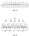
- the metal layer 104 may be patterned before laser welding and ablation. This is schematically illustrated in FIG. 13 , where the metal layer 104 is formed on the P-type and N-type doped regions without electrically connecting them.
- the metal layer 104 may be deposited by blanket deposition over the dielectric spacers 103, the N-type doped regions, and the P-type doped regions, and then patterned (e.g., by masking and etching) to separate the N-type doped regions from the P-type doped regions as shown in FIG. 13 .
- the metal foil 105 may then be placed on the patterned metal layer 104 and dielectric spacers 103, laser welded to the metal layer 104, and patterned by laser ablation as previously described.
- FIG. 14 schematically shows the N-type metal fingers 108 and P-type metal fingers 109 after the laser ablation process in that embodiment. The laser ablation process cuts through the metal foil 105 but stops at the dielectric spacers 103.
Landscapes
- Engineering & Computer Science (AREA)
- Sustainable Development (AREA)
- Life Sciences & Earth Sciences (AREA)
- Physics & Mathematics (AREA)
- Microelectronics & Electronic Packaging (AREA)
- Condensed Matter Physics & Semiconductors (AREA)
- Electromagnetism (AREA)
- General Physics & Mathematics (AREA)
- Power Engineering (AREA)
- Computer Hardware Design (AREA)
- Sustainable Energy (AREA)
- Crystallography & Structural Chemistry (AREA)
- Chemical & Material Sciences (AREA)
- Photovoltaic Devices (AREA)
- Electrodes Of Semiconductors (AREA)
- Laminated Bodies (AREA)
- Manufacturing & Machinery (AREA)
Applications Claiming Priority (2)
| Application Number | Priority Date | Filing Date | Title |
|---|---|---|---|
| US14/040,047 US9437756B2 (en) | 2013-09-27 | 2013-09-27 | Metallization of solar cells using metal foils |
| PCT/US2014/056794 WO2015047952A1 (en) | 2013-09-27 | 2014-09-22 | Metallization of solar cells using metal foils |
Publications (3)
| Publication Number | Publication Date |
|---|---|
| EP3050122A1 EP3050122A1 (en) | 2016-08-03 |
| EP3050122A4 EP3050122A4 (en) | 2016-09-21 |
| EP3050122B1 true EP3050122B1 (en) | 2020-06-17 |
Family
ID=52738910
Family Applications (1)
| Application Number | Title | Priority Date | Filing Date |
|---|---|---|---|
| EP14847743.3A Active EP3050122B1 (en) | 2013-09-27 | 2014-09-22 | Metallization of solar cells using metal foils |
Country Status (14)
| Country | Link |
|---|---|
| US (3) | US9437756B2 (ja) |
| EP (1) | EP3050122B1 (ja) |
| JP (1) | JP6526020B2 (ja) |
| KR (1) | KR102313263B1 (ja) |
| CN (2) | CN105474412B (ja) |
| AU (1) | AU2014327036B2 (ja) |
| BR (1) | BR112016006585B1 (ja) |
| CL (1) | CL2016000712A1 (ja) |
| MX (1) | MX356833B (ja) |
| MY (1) | MY175353A (ja) |
| SA (1) | SA516370630B1 (ja) |
| SG (1) | SG11201601079QA (ja) |
| TW (1) | TWI633677B (ja) |
| WO (1) | WO2015047952A1 (ja) |
Families Citing this family (36)
| Publication number | Priority date | Publication date | Assignee | Title |
|---|---|---|---|---|
| KR101620431B1 (ko) * | 2014-01-29 | 2016-05-12 | 엘지전자 주식회사 | 태양 전지 및 이의 제조 방법 |
| US9911874B2 (en) * | 2014-05-30 | 2018-03-06 | Sunpower Corporation | Alignment free solar cell metallization |
| CN106687617B (zh) * | 2014-07-15 | 2020-04-07 | 奈特考尔技术公司 | 激光转印ibc太阳能电池 |
| US9461192B2 (en) | 2014-12-16 | 2016-10-04 | Sunpower Corporation | Thick damage buffer for foil-based metallization of solar cells |
| US9620661B2 (en) | 2014-12-19 | 2017-04-11 | Sunpower Corporation | Laser beam shaping for foil-based metallization of solar cells |
| US9997651B2 (en) | 2015-02-19 | 2018-06-12 | Sunpower Corporation | Damage buffer for solar cell metallization |
| US20160380120A1 (en) | 2015-06-26 | 2016-12-29 | Akira Terao | Metallization and stringing for back-contact solar cells |
| US9722103B2 (en) * | 2015-06-26 | 2017-08-01 | Sunpower Corporation | Thermal compression bonding approaches for foil-based metallization of solar cells |
| US9634178B1 (en) * | 2015-12-16 | 2017-04-25 | Sunpower Corporation | Method of using laser welding to ohmic contact of metallic thermal and diffusion barrier layer for foil-based metallization of solar cells |
| US9831377B2 (en) | 2016-02-29 | 2017-11-28 | Sunpower Corporation | Die-cutting approaches for foil-based metallization of solar cells |
| US11424373B2 (en) | 2016-04-01 | 2022-08-23 | Sunpower Corporation | Thermocompression bonding approaches for foil-based metallization of non-metal surfaces of solar cells |
| DE102016107802A1 (de) | 2016-04-27 | 2017-11-02 | Universität Stuttgart | Verfahren zur Herstellung rückseitenkontaktierter Solarzellen aus kristallinem Silizium |
| US20180006172A1 (en) * | 2016-07-01 | 2018-01-04 | Sunpower Corporation | Metallization structures for solar cells |
| US9871150B1 (en) * | 2016-07-01 | 2018-01-16 | Sunpower Corporation | Protective region for metallization of solar cells |
| US9882071B2 (en) * | 2016-07-01 | 2018-01-30 | Sunpower Corporation | Laser techniques for foil-based metallization of solar cells |
| USD822890S1 (en) | 2016-09-07 | 2018-07-10 | Felxtronics Ap, Llc | Lighting apparatus |
| US10115855B2 (en) * | 2016-09-30 | 2018-10-30 | Sunpower Corporation | Conductive foil based metallization of solar cells |
| US10775030B2 (en) | 2017-05-05 | 2020-09-15 | Flex Ltd. | Light fixture device including rotatable light modules |
| USD833061S1 (en) | 2017-08-09 | 2018-11-06 | Flex Ltd. | Lighting module locking endcap |
| USD862777S1 (en) | 2017-08-09 | 2019-10-08 | Flex Ltd. | Lighting module wide distribution lens |
| USD872319S1 (en) | 2017-08-09 | 2020-01-07 | Flex Ltd. | Lighting module LED light board |
| USD846793S1 (en) | 2017-08-09 | 2019-04-23 | Flex Ltd. | Lighting module locking mechanism |
| USD877964S1 (en) | 2017-08-09 | 2020-03-10 | Flex Ltd. | Lighting module |
| USD832494S1 (en) | 2017-08-09 | 2018-10-30 | Flex Ltd. | Lighting module heatsink |
| USD832495S1 (en) | 2017-08-18 | 2018-10-30 | Flex Ltd. | Lighting module locking mechanism |
| USD862778S1 (en) | 2017-08-22 | 2019-10-08 | Flex Ltd | Lighting module lens |
| USD888323S1 (en) | 2017-09-07 | 2020-06-23 | Flex Ltd | Lighting module wire guard |
| WO2019195806A2 (en) | 2018-04-06 | 2019-10-10 | Sunpower Corporation | Local patterning and metallization of semiconductor structures using a laser beam |
| WO2019195793A1 (en) * | 2018-04-06 | 2019-10-10 | Sunpower Corporation | Laser assisted metallization process for solar cell stringing |
| CN112424956A (zh) * | 2018-04-06 | 2021-02-26 | 太阳能公司 | 使用激光束对半导体基板进行局部金属化 |
| US11276785B2 (en) | 2018-04-06 | 2022-03-15 | Sunpower Corporation | Laser assisted metallization process for solar cell fabrication |
| US11646387B2 (en) * | 2018-04-06 | 2023-05-09 | Maxeon Solar Pte. Ltd. | Laser assisted metallization process for solar cell circuit formation |
| CN108873172A (zh) * | 2018-06-29 | 2018-11-23 | 中国科学院上海光学精密机械研究所 | 一种片上电可调高品质薄膜微光学器件的制备方法 |
| EP3588584A1 (en) | 2018-06-29 | 2020-01-01 | Total SA | Solar cells and metallization process and device |
| WO2020205983A1 (en) * | 2019-04-01 | 2020-10-08 | Stinger Advanced Manufacturing Corporation | Systems and methods for non-continuous deposition of a component |
| US11527611B2 (en) | 2020-11-09 | 2022-12-13 | The Aerospace Corporation | Method of forming nanowire connects on (photovoltiac) PV cells |
Family Cites Families (110)
| Publication number | Priority date | Publication date | Assignee | Title |
|---|---|---|---|---|
| US4058418A (en) | 1974-04-01 | 1977-11-15 | Solarex Corporation | Fabrication of thin film solar cells utilizing epitaxial deposition onto a liquid surface to obtain lateral growth |
| US3993533A (en) | 1975-04-09 | 1976-11-23 | Carnegie-Mellon University | Method for making semiconductors for solar cells |
| US4318938A (en) | 1979-05-29 | 1982-03-09 | The University Of Delaware | Method for the continuous manufacture of thin film solar cells |
| DE3036260A1 (de) | 1980-09-26 | 1982-04-29 | Licentia Patent-Verwaltungs-Gmbh, 6000 Frankfurt | Verfahren zur herstellung von elektrischen kontakten an einer silizium-solarzelle |
| US4400577A (en) | 1981-07-16 | 1983-08-23 | Spear Reginald G | Thin solar cells |
| US4433200A (en) | 1981-10-02 | 1984-02-21 | Atlantic Richfield Company | Roll formed pan solar module |
| US4482780A (en) | 1982-11-30 | 1984-11-13 | The United States Of America As Represented By The United States Department Of Energy | Solar cells with low cost substrates and process of making same |
| US4461922A (en) | 1983-02-14 | 1984-07-24 | Atlantic Richfield Company | Solar cell module |
| US4511600A (en) | 1984-02-10 | 1985-04-16 | Solarex Corporation | Solar cell metal spray process |
| US4957601A (en) | 1984-09-04 | 1990-09-18 | Texas Instruments Incorporated | Method of forming an array of apertures in an aluminum foil |
| US4691076A (en) | 1984-09-04 | 1987-09-01 | Texas Instruments Incorporated | Solar array with aluminum foil matrix |
| US4917752A (en) | 1984-09-04 | 1990-04-17 | Texas Instruments Incorporated | Method of forming contacts on semiconductor members |
| US4581103A (en) | 1984-09-04 | 1986-04-08 | Texas Instruments Incorporated | Method of etching semiconductor material |
| US4582588A (en) | 1984-09-04 | 1986-04-15 | Texas Instruments Incorporated | Method of anodizing and sealing aluminum |
| US4697041A (en) | 1985-02-15 | 1987-09-29 | Teijin Limited | Integrated solar cells |
| US4617421A (en) | 1985-04-01 | 1986-10-14 | Sovonics Solar Systems | Photovoltaic cell having increased active area and method for producing same |
| US4695674A (en) | 1985-08-30 | 1987-09-22 | The Standard Oil Company | Preformed, thin-film front contact current collector grid for photovoltaic cells |
| DE3725269A1 (de) | 1987-07-30 | 1989-02-09 | Messerschmitt Boelkow Blohm | Verfahren zum einkapseln von mikroelektronischen halbleiter- und schichtschaltungen |
| US5010040A (en) | 1988-12-30 | 1991-04-23 | Mobil Solar Energy Corporation | Method of fabricating solar cells |
| US5091319A (en) | 1989-07-31 | 1992-02-25 | Hotchkiss Gregory B | Method of affixing silicon spheres to a foil matrix |
| US5011567A (en) | 1989-12-06 | 1991-04-30 | Mobil Solar Energy Corporation | Method of fabricating solar cells |
| US5032233A (en) | 1990-09-05 | 1991-07-16 | Micron Technology, Inc. | Method for improving step coverage of a metallization layer on an integrated circuit by use of a high melting point metal as an anti-reflective coating during laser planarization |
| US5093279A (en) | 1991-02-01 | 1992-03-03 | International Business Machines Corporation | Laser ablation damascene process |
| AU651486B2 (en) | 1991-08-30 | 1994-07-21 | Canon Kabushiki Kaisha | Photoelectric conversion element and fabrication method thereof |
| US5472772A (en) | 1994-04-18 | 1995-12-05 | General Electric Company | Method for welding stacker laminations and article therefrom |
| US6141497A (en) | 1995-06-09 | 2000-10-31 | Marotta Scientific Controls, Inc. | Multilayer micro-gas rheostat with electrical-heater control of gas flow |
| US6387803B2 (en) | 1997-01-29 | 2002-05-14 | Ultratech Stepper, Inc. | Method for forming a silicide region on a silicon body |
| WO1998037740A1 (en) | 1997-02-21 | 1998-08-27 | Koninklijke Philips Electronics N.V. | A method of selectively metallizing a substrate using a hot foil embossing technique |
| US5951786A (en) | 1997-12-19 | 1999-09-14 | Sandia Corporation | Laminated photovoltaic modules using back-contact solar cells |
| JPH11243224A (ja) | 1997-12-26 | 1999-09-07 | Canon Inc | 光起電力素子モジュール及びその製造方法並びに非接触処理方法 |
| EP1051885A1 (en) | 1998-02-06 | 2000-11-15 | FLEXcon Company, Inc. | Thin film transferable electric components |
| US6159832A (en) | 1998-03-18 | 2000-12-12 | Mayer; Frederick J. | Precision laser metallization |
| US6175075B1 (en) | 1998-04-21 | 2001-01-16 | Canon Kabushiki Kaisha | Solar cell module excelling in reliability |
| DE60034840T3 (de) | 1999-03-23 | 2011-02-24 | Kaneka Corp., Osaka-shi | Photovoltaisches Modul |
| JP2001007362A (ja) | 1999-06-17 | 2001-01-12 | Canon Inc | 半導体基材および太陽電池の製造方法 |
| US6825550B2 (en) | 1999-09-02 | 2004-11-30 | Micron Technology, Inc. | Board-on-chip packages with conductive foil on the chip surface |
| AU2001282581A1 (en) | 2000-09-01 | 2002-03-13 | Showa Denko K K | Apparatus for producing capacitor element member |
| AU2002238953B2 (en) | 2001-03-19 | 2007-03-29 | Shin-Etsu Chemical Co., Ltd | Solar cell and its manufacturing method |
| WO2003032957A2 (en) | 2001-06-28 | 2003-04-24 | Microchips, Inc. | Methods for hermetically sealing microchip reservoir devices |
| JP3809353B2 (ja) | 2001-08-02 | 2006-08-16 | キヤノン株式会社 | Id付き加工物の製造方法 |
| US7106939B2 (en) | 2001-09-19 | 2006-09-12 | 3M Innovative Properties Company | Optical and optoelectronic articles |
| US6635307B2 (en) | 2001-12-12 | 2003-10-21 | Nanotek Instruments, Inc. | Manufacturing method for thin-film solar cells |
| US20060166023A1 (en) | 2002-09-06 | 2006-07-27 | Dai Nippon Printing Co., Ltd. | Backside protective sheet for solar battery module and solar battery module using the same |
| JP2004103959A (ja) | 2002-09-11 | 2004-04-02 | Matsushita Electric Ind Co Ltd | 太陽電池およびその製造方法 |
| DE10245928B4 (de) | 2002-09-30 | 2006-03-23 | Infineon Technologies Ag | Verfahren zur strukturierten, selektiven Matallisierung einer Oberfläche eines Substrats |
| US8222072B2 (en) * | 2002-12-20 | 2012-07-17 | The Trustees Of Princeton University | Methods of fabricating devices by low pressure cold welding |
| US7388147B2 (en) * | 2003-04-10 | 2008-06-17 | Sunpower Corporation | Metal contact structure for solar cell and method of manufacture |
| EP1634673A4 (en) | 2003-04-25 | 2009-04-08 | Nitto Denko Corp | METHOD FOR PRODUCING A LASER-TREATED PRODUCT AND AN ADHESIVE SHEET FOR A LASER TREATMENT USED FOR THIS PRODUCT |
| US7494896B2 (en) | 2003-06-12 | 2009-02-24 | International Business Machines Corporation | Method of forming magnetic random access memory (MRAM) devices on thermally-sensitive substrates using laser transfer |
| DE10349749B3 (de) | 2003-10-23 | 2005-05-25 | Infineon Technologies Ag | Anti-Fuse-Verbindung für integrierte Schaltungen sowie Verfahren zur Herstellung von Anti-Fuse-Verbindungen |
| JP4059842B2 (ja) * | 2003-12-05 | 2008-03-12 | シャープ株式会社 | 太陽電池セルおよび太陽電池モジュール |
| KR100610462B1 (ko) | 2004-02-20 | 2006-08-08 | 엔이씨 도낀 가부시끼가이샤 | 고체 전해 커패시터, 전송선로장치, 그 제조방법 및 그것을이용하는 복합 전자부품 |
| KR100594277B1 (ko) * | 2004-05-25 | 2006-06-30 | 삼성전자주식회사 | 포토 다이오드 및 그 제조방법 |
| JP2006040938A (ja) | 2004-07-22 | 2006-02-09 | Nec Tokin Corp | 固体電解コンデンサ、それを用いた積層コンデンサおよびその製造方法 |
| US20080223429A1 (en) | 2004-08-09 | 2008-09-18 | The Australian National University | Solar Cell (Sliver) Sub-Module Formation |
| DE102004050269A1 (de) * | 2004-10-14 | 2006-04-20 | Institut Für Solarenergieforschung Gmbh | Verfahren zur Kontakttrennung elektrisch leitfähiger Schichten auf rückkontaktierten Solarzellen und Solarzelle |
| US7358151B2 (en) | 2004-12-21 | 2008-04-15 | Sony Corporation | Microelectromechanical system microphone fabrication including signal processing circuitry on common substrate |
| US7554055B2 (en) | 2005-05-03 | 2009-06-30 | Hitachi Global Storage Technologies Netherlands B.V. | Method for making ohmic contact to silicon structures with low thermal loads |
| JP2006324555A (ja) | 2005-05-20 | 2006-11-30 | Nec Tokin Corp | 積層型コンデンサ及びその製造方法 |
| DE102005041099A1 (de) | 2005-08-30 | 2007-03-29 | Osram Opto Semiconductors Gmbh | LED-Chip mit Glasbeschichtung und planarer Aufbau- und Verbindungstechnik |
| US20070295399A1 (en) * | 2005-12-16 | 2007-12-27 | Bp Corporation North America Inc. | Back-Contact Photovoltaic Cells |
| JP4842118B2 (ja) | 2006-01-24 | 2011-12-21 | ルネサスエレクトロニクス株式会社 | 半導体装置の製造方法 |
| US7795600B2 (en) | 2006-03-24 | 2010-09-14 | Goldeneye, Inc. | Wavelength conversion chip for use with light emitting diodes and method for making same |
| DE102006040352B3 (de) | 2006-08-29 | 2007-10-18 | Fraunhofer-Gesellschaft zur Förderung der angewandten Forschung e.V. | Verfahren zum Aufbringen von elektrischen Kontakten auf halbleitende Substrate, halbleitendes Substrat und Verwendung des Verfahrens |
| DE102006044936B4 (de) | 2006-09-22 | 2008-08-07 | Fraunhofer-Gesellschaft zur Förderung der angewandten Forschung e.V. | Verfahren zur Metallisierung von Solarzellen und dessen Verwendung |
| US20080128019A1 (en) | 2006-12-01 | 2008-06-05 | Applied Materials, Inc. | Method of metallizing a solar cell substrate |
| WO2008069456A1 (en) | 2006-12-05 | 2008-06-12 | Electronics And Telecommunications Research Institute | Planar lightwave circuit(plc) device, wavelength tunable light source comprising the same device and wavelength division multiplexing-passive optical network(wdm-pon) using the same light source |
| EP2100336A4 (en) | 2006-12-22 | 2013-04-10 | Applied Materials Inc | INTERCONNECTION TECHNOLOGIES FOR REAR CONTACT SOLAR CELLS AND MODULES |
| US7755292B1 (en) | 2007-01-22 | 2010-07-13 | The United States Of America As Represented By The Administrator Of The National Aeronautics And Space Administration | Ultraminiature broadband light source and method of manufacturing same |
| US8066840B2 (en) * | 2007-01-22 | 2011-11-29 | Solopower, Inc. | Finger pattern formation for thin film solar cells |
| US7804022B2 (en) | 2007-03-16 | 2010-09-28 | Sunpower Corporation | Solar cell contact fingers and solder pad arrangement for enhanced efficiency |
| CN101689580B (zh) | 2007-03-16 | 2012-09-05 | Bp北美公司 | 太阳能电池 |
| US8471141B2 (en) * | 2007-05-07 | 2013-06-25 | Nanosolar, Inc | Structures for low cost, reliable solar roofing |
| US8866150B2 (en) | 2007-05-31 | 2014-10-21 | Cree, Inc. | Silicon carbide power devices including P-type epitaxial layers and direct ohmic contacts |
| TWI450401B (zh) | 2007-08-28 | 2014-08-21 | Mosel Vitelic Inc | 太陽能電池及其製造方法 |
| JP5252472B2 (ja) | 2007-09-28 | 2013-07-31 | シャープ株式会社 | 太陽電池、太陽電池の製造方法、太陽電池モジュールの製造方法および太陽電池モジュール |
| US20120125256A1 (en) | 2007-10-06 | 2012-05-24 | Solexel, Inc. | Apparatus and method for repeatedly fabricating thin film semiconductor substrates using a template |
| JP2009130116A (ja) | 2007-11-22 | 2009-06-11 | Sharp Corp | 素子間配線部材、光電変換素子およびこれらを用いた光電変換素子接続体ならびに光電変換モジュール |
| EP2239788A4 (en) * | 2008-01-30 | 2017-07-12 | Kyocera Corporation | Solar battery element and solar battery element manufacturing method |
| JP4870100B2 (ja) | 2008-01-30 | 2012-02-08 | 日清紡ホールディングス株式会社 | テープ状体の配設装置 |
| US8481845B2 (en) | 2008-02-05 | 2013-07-09 | Gtat Corporation | Method to form a photovoltaic cell comprising a thin lamina |
| DE102008013446A1 (de) * | 2008-02-15 | 2009-08-27 | Ersol Solar Energy Ag | Verfahren zur Herstellung monokristalliner n-Silizium-Solarzellen sowie Solarzelle, hergestellt nach einem derartigen Verfahren |
| US20110192445A1 (en) | 2008-03-13 | 2011-08-11 | Florian Solzbacher | High precision, high speed solar cell arrangement to a concentrator lens array and methods of making the same |
| US8309388B2 (en) | 2008-04-25 | 2012-11-13 | Texas Instruments Incorporated | MEMS package having formed metal lid |
| DE102008021167B3 (de) | 2008-04-28 | 2010-01-21 | Siemens Aktiengesellschaft | Verfahren zur Erzeugung einer hermetisch dichten, elektrischen Durchführung mittels exothermer Nanofolie und damit hergestellte Vorrichtung |
| US7851698B2 (en) * | 2008-06-12 | 2010-12-14 | Sunpower Corporation | Trench process and structure for backside contact solar cells with polysilicon doped regions |
| JP2010028017A (ja) | 2008-07-24 | 2010-02-04 | Fuji Electric Device Technology Co Ltd | 薄型インダクタおよびその製造方法と、この薄型インダクタを用いた超小型電力変換装置 |
| DE102008062591A1 (de) | 2008-08-08 | 2010-03-04 | Deutsche Cell Gmbh | Halbleiter-Bauelement |
| US7951637B2 (en) * | 2008-08-27 | 2011-05-31 | Applied Materials, Inc. | Back contact solar cells using printed dielectric barrier |
| WO2010025269A1 (en) | 2008-08-27 | 2010-03-04 | Applied Materials, Inc. | Back contact solar cell modules |
| KR101639786B1 (ko) | 2009-01-14 | 2016-07-15 | 코닌클리케 필립스 엔.브이. | 기판 상에 적어도 하나의 전기 전도성 막을 퇴적하는 방법 |
| US8207443B2 (en) | 2009-01-27 | 2012-06-26 | Applied Materials, Inc. | Point contacts for polysilicon emitter solar cell |
| EP2412030A2 (en) | 2009-03-26 | 2012-02-01 | BP Corporation North America Inc. | Apparatus and method for solar cells with laser fired contacts in thermally diffused doped regions |
| US8021919B2 (en) | 2009-03-31 | 2011-09-20 | Infineon Technologies Ag | Method of manufacturing a semiconductor device |
| JP2011054831A (ja) | 2009-09-03 | 2011-03-17 | Sharp Corp | バックコンタクト型太陽電池セル、太陽電池ストリングおよび太陽電池モジュール |
| KR20110047861A (ko) * | 2009-10-30 | 2011-05-09 | 삼성전자주식회사 | 태양 전지 및 이의 제조 방법 |
| FR2957479B1 (fr) | 2010-03-12 | 2012-04-27 | Commissariat Energie Atomique | Procede de traitement d'un contact metallique realise sur un substrat |
| MY158500A (en) | 2010-08-05 | 2016-10-14 | Solexel Inc | Backplane reinforcement and interconnects for solar cells |
| KR101172195B1 (ko) | 2010-09-16 | 2012-08-07 | 엘지이노텍 주식회사 | 태양광 발전장치 및 이의 제조방법 |
| US8975510B2 (en) | 2011-03-25 | 2015-03-10 | Cellink Corporation | Foil-based interconnect for rear-contact solar cells |
| US20130137244A1 (en) | 2011-05-26 | 2013-05-30 | Solexel, Inc. | Method and apparatus for reconditioning a carrier wafer for reuse |
| DE102011104159A1 (de) | 2011-06-14 | 2012-12-20 | Institut Für Solarenergieforschung Gmbh | Verfahren zum elektrischen verbinden mehrerer solarzellen und photovoltaikmodul |
| US20130228221A1 (en) | 2011-08-05 | 2013-09-05 | Solexel, Inc. | Manufacturing methods and structures for large-area thin-film solar cells and other semiconductor devices |
| US8563364B2 (en) | 2011-09-29 | 2013-10-22 | Infineon Technologies Ag | Method for producing a power semiconductor arrangement |
| US20130160825A1 (en) | 2011-12-22 | 2013-06-27 | E I Du Pont De Nemours And Company | Back contact photovoltaic module with glass back-sheet |
| WO2013106225A1 (en) | 2012-01-12 | 2013-07-18 | Applied Materials, Inc. | Methods of manufacturing solar cell devices |
| US8513045B1 (en) * | 2012-01-31 | 2013-08-20 | Sunpower Corporation | Laser system with multiple laser pulses for fabrication of solar cells |
| CN104170095B (zh) * | 2012-03-14 | 2016-10-19 | Imec非营利协会 | 用于制造具有镀敷触点的光伏电池的方法 |
| US8859322B2 (en) | 2012-03-19 | 2014-10-14 | Rec Solar Pte. Ltd. | Cell and module processing of semiconductor wafers for back-contacted solar photovoltaic module |
| US9040409B2 (en) | 2013-03-15 | 2015-05-26 | Applied Materials, Inc. | Methods of forming solar cells and solar cell modules |
-
2013
- 2013-09-27 US US14/040,047 patent/US9437756B2/en active Active
-
2014
- 2014-09-22 EP EP14847743.3A patent/EP3050122B1/en active Active
- 2014-09-22 CN CN201480046849.0A patent/CN105474412B/zh active Active
- 2014-09-22 BR BR112016006585-9A patent/BR112016006585B1/pt active IP Right Grant
- 2014-09-22 MY MYPI2016000345A patent/MY175353A/en unknown
- 2014-09-22 MX MX2016003561A patent/MX356833B/es active IP Right Grant
- 2014-09-22 JP JP2016545766A patent/JP6526020B2/ja active Active
- 2014-09-22 WO PCT/US2014/056794 patent/WO2015047952A1/en active Application Filing
- 2014-09-22 SG SG11201601079QA patent/SG11201601079QA/en unknown
- 2014-09-22 AU AU2014327036A patent/AU2014327036B2/en active Active
- 2014-09-22 CN CN201711214605.0A patent/CN108039380B/zh active Active
- 2014-09-22 KR KR1020167010446A patent/KR102313263B1/ko active IP Right Grant
- 2014-09-23 TW TW103132752A patent/TWI633677B/zh active
-
2016
- 2016-02-27 SA SA516370630A patent/SA516370630B1/ar unknown
- 2016-03-24 CL CL2016000712A patent/CL2016000712A1/es unknown
- 2016-08-05 US US15/230,163 patent/US9865753B2/en active Active
-
2017
- 2017-12-05 US US15/832,447 patent/US10930804B2/en active Active
Non-Patent Citations (1)
| Title |
|---|
| None * |
Also Published As
| Publication number | Publication date |
|---|---|
| MX2016003561A (es) | 2016-06-02 |
| WO2015047952A1 (en) | 2015-04-02 |
| CN105474412A (zh) | 2016-04-06 |
| AU2014327036B2 (en) | 2018-07-05 |
| EP3050122A4 (en) | 2016-09-21 |
| CL2016000712A1 (es) | 2016-12-16 |
| TWI633677B (zh) | 2018-08-21 |
| MX356833B (es) | 2018-06-15 |
| US9865753B2 (en) | 2018-01-09 |
| KR102313263B1 (ko) | 2021-10-14 |
| BR112016006585A2 (pt) | 2017-08-01 |
| CN108039380B (zh) | 2020-07-10 |
| US10930804B2 (en) | 2021-02-23 |
| EP3050122A1 (en) | 2016-08-03 |
| US20150090329A1 (en) | 2015-04-02 |
| US20180097129A1 (en) | 2018-04-05 |
| SA516370630B1 (ar) | 2019-04-11 |
| TW201521220A (zh) | 2015-06-01 |
| CN105474412B (zh) | 2018-01-02 |
| SG11201601079QA (en) | 2016-03-30 |
| BR112016006585B1 (pt) | 2021-08-03 |
| AU2014327036A1 (en) | 2015-12-17 |
| US20160343888A1 (en) | 2016-11-24 |
| MY175353A (en) | 2020-06-22 |
| CN108039380A (zh) | 2018-05-15 |
| JP6526020B2 (ja) | 2019-06-05 |
| US9437756B2 (en) | 2016-09-06 |
| KR20160061368A (ko) | 2016-05-31 |
| JP2016536808A (ja) | 2016-11-24 |
Similar Documents
| Publication | Publication Date | Title |
|---|---|---|
| EP3050122B1 (en) | Metallization of solar cells using metal foils | |
| US11784264B2 (en) | Single-step metal bond and contact formation for solar cells | |
| KR20160024973A (ko) | 광기전 전지 및 라미네이트 금속화 | |
| KR20140015247A (ko) | 태양전지용 백플레인 보강 및 상호연결부 | |
| KR20140027188A (ko) | 박형 실리콘 태양 전지용 활성 후면판 | |
| CN112136218A (zh) | 用于太阳能电池电路形成的激光辅助金属化工艺 | |
| CN107466427B (zh) | 用于太阳能电池金属化的损伤缓冲结构 | |
| JP2010062186A (ja) | 光電変換装置およびその製造方法 | |
| US9171989B2 (en) | Metal bond and contact formation for solar cells | |
| TWI645575B (zh) | 太陽能電池之單步驟金屬接合及接觸形成 |
Legal Events
| Date | Code | Title | Description |
|---|---|---|---|
| PUAI | Public reference made under article 153(3) epc to a published international application that has entered the european phase |
Free format text: ORIGINAL CODE: 0009012 |
|
| 17P | Request for examination filed |
Effective date: 20160226 |
|
| AK | Designated contracting states |
Kind code of ref document: A1 Designated state(s): AL AT BE BG CH CY CZ DE DK EE ES FI FR GB GR HR HU IE IS IT LI LT LU LV MC MK MT NL NO PL PT RO RS SE SI SK SM TR |
|
| AX | Request for extension of the european patent |
Extension state: BA ME |
|
| A4 | Supplementary search report drawn up and despatched |
Effective date: 20160819 |
|
| RIC1 | Information provided on ipc code assigned before grant |
Ipc: H01L 31/042 20060101AFI20160815BHEP Ipc: H01L 31/18 20060101ALI20160815BHEP Ipc: H01L 31/0224 20060101ALI20160815BHEP |
|
| DAX | Request for extension of the european patent (deleted) | ||
| STAA | Information on the status of an ep patent application or granted ep patent |
Free format text: STATUS: EXAMINATION IS IN PROGRESS |
|
| 17Q | First examination report despatched |
Effective date: 20190521 |
|
| REG | Reference to a national code |
Ref country code: DE Ref legal event code: R079 Ref document number: 602014066819 Country of ref document: DE Free format text: PREVIOUS MAIN CLASS: H01L0031042000 Ipc: H01L0031050000 |
|
| GRAP | Despatch of communication of intention to grant a patent |
Free format text: ORIGINAL CODE: EPIDOSNIGR1 |
|
| STAA | Information on the status of an ep patent application or granted ep patent |
Free format text: STATUS: GRANT OF PATENT IS INTENDED |
|
| RIC1 | Information provided on ipc code assigned before grant |
Ipc: H01L 31/18 20060101ALI20191212BHEP Ipc: H01L 31/0224 20060101ALI20191212BHEP Ipc: H01L 31/042 20140101ALI20191212BHEP Ipc: H01L 31/05 20140101AFI20191212BHEP |
|
| INTG | Intention to grant announced |
Effective date: 20200107 |
|
| GRAS | Grant fee paid |
Free format text: ORIGINAL CODE: EPIDOSNIGR3 |
|
| GRAA | (expected) grant |
Free format text: ORIGINAL CODE: 0009210 |
|
| STAA | Information on the status of an ep patent application or granted ep patent |
Free format text: STATUS: THE PATENT HAS BEEN GRANTED |
|
| AK | Designated contracting states |
Kind code of ref document: B1 Designated state(s): AL AT BE BG CH CY CZ DE DK EE ES FI FR GB GR HR HU IE IS IT LI LT LU LV MC MK MT NL NO PL PT RO RS SE SI SK SM TR |
|
| REG | Reference to a national code |
Ref country code: GB Ref legal event code: FG4D |
|
| REG | Reference to a national code |
Ref country code: CH Ref legal event code: EP |
|
| REG | Reference to a national code |
Ref country code: IE Ref legal event code: FG4D |
|
| REG | Reference to a national code |
Ref country code: DE Ref legal event code: R096 Ref document number: 602014066819 Country of ref document: DE |
|
| REG | Reference to a national code |
Ref country code: AT Ref legal event code: REF Ref document number: 1282394 Country of ref document: AT Kind code of ref document: T Effective date: 20200715 |
|
| PG25 | Lapsed in a contracting state [announced via postgrant information from national office to epo] |
Ref country code: SE Free format text: LAPSE BECAUSE OF FAILURE TO SUBMIT A TRANSLATION OF THE DESCRIPTION OR TO PAY THE FEE WITHIN THE PRESCRIBED TIME-LIMIT Effective date: 20200617 Ref country code: LT Free format text: LAPSE BECAUSE OF FAILURE TO SUBMIT A TRANSLATION OF THE DESCRIPTION OR TO PAY THE FEE WITHIN THE PRESCRIBED TIME-LIMIT Effective date: 20200617 Ref country code: FI Free format text: LAPSE BECAUSE OF FAILURE TO SUBMIT A TRANSLATION OF THE DESCRIPTION OR TO PAY THE FEE WITHIN THE PRESCRIBED TIME-LIMIT Effective date: 20200617 Ref country code: NO Free format text: LAPSE BECAUSE OF FAILURE TO SUBMIT A TRANSLATION OF THE DESCRIPTION OR TO PAY THE FEE WITHIN THE PRESCRIBED TIME-LIMIT Effective date: 20200917 Ref country code: GR Free format text: LAPSE BECAUSE OF FAILURE TO SUBMIT A TRANSLATION OF THE DESCRIPTION OR TO PAY THE FEE WITHIN THE PRESCRIBED TIME-LIMIT Effective date: 20200918 |
|
| REG | Reference to a national code |
Ref country code: LT Ref legal event code: MG4D |
|
| REG | Reference to a national code |
Ref country code: NL Ref legal event code: MP Effective date: 20200617 |
|
| PG25 | Lapsed in a contracting state [announced via postgrant information from national office to epo] |
Ref country code: LV Free format text: LAPSE BECAUSE OF FAILURE TO SUBMIT A TRANSLATION OF THE DESCRIPTION OR TO PAY THE FEE WITHIN THE PRESCRIBED TIME-LIMIT Effective date: 20200617 Ref country code: RS Free format text: LAPSE BECAUSE OF FAILURE TO SUBMIT A TRANSLATION OF THE DESCRIPTION OR TO PAY THE FEE WITHIN THE PRESCRIBED TIME-LIMIT Effective date: 20200617 Ref country code: BG Free format text: LAPSE BECAUSE OF FAILURE TO SUBMIT A TRANSLATION OF THE DESCRIPTION OR TO PAY THE FEE WITHIN THE PRESCRIBED TIME-LIMIT Effective date: 20200917 Ref country code: HR Free format text: LAPSE BECAUSE OF FAILURE TO SUBMIT A TRANSLATION OF THE DESCRIPTION OR TO PAY THE FEE WITHIN THE PRESCRIBED TIME-LIMIT Effective date: 20200617 |
|
| REG | Reference to a national code |
Ref country code: AT Ref legal event code: MK05 Ref document number: 1282394 Country of ref document: AT Kind code of ref document: T Effective date: 20200617 |
|
| PG25 | Lapsed in a contracting state [announced via postgrant information from national office to epo] |
Ref country code: NL Free format text: LAPSE BECAUSE OF FAILURE TO SUBMIT A TRANSLATION OF THE DESCRIPTION OR TO PAY THE FEE WITHIN THE PRESCRIBED TIME-LIMIT Effective date: 20200617 Ref country code: AL Free format text: LAPSE BECAUSE OF FAILURE TO SUBMIT A TRANSLATION OF THE DESCRIPTION OR TO PAY THE FEE WITHIN THE PRESCRIBED TIME-LIMIT Effective date: 20200617 |
|
| PG25 | Lapsed in a contracting state [announced via postgrant information from national office to epo] |
Ref country code: CZ Free format text: LAPSE BECAUSE OF FAILURE TO SUBMIT A TRANSLATION OF THE DESCRIPTION OR TO PAY THE FEE WITHIN THE PRESCRIBED TIME-LIMIT Effective date: 20200617 Ref country code: IT Free format text: LAPSE BECAUSE OF FAILURE TO SUBMIT A TRANSLATION OF THE DESCRIPTION OR TO PAY THE FEE WITHIN THE PRESCRIBED TIME-LIMIT Effective date: 20200617 Ref country code: RO Free format text: LAPSE BECAUSE OF FAILURE TO SUBMIT A TRANSLATION OF THE DESCRIPTION OR TO PAY THE FEE WITHIN THE PRESCRIBED TIME-LIMIT Effective date: 20200617 Ref country code: SM Free format text: LAPSE BECAUSE OF FAILURE TO SUBMIT A TRANSLATION OF THE DESCRIPTION OR TO PAY THE FEE WITHIN THE PRESCRIBED TIME-LIMIT Effective date: 20200617 Ref country code: EE Free format text: LAPSE BECAUSE OF FAILURE TO SUBMIT A TRANSLATION OF THE DESCRIPTION OR TO PAY THE FEE WITHIN THE PRESCRIBED TIME-LIMIT Effective date: 20200617 Ref country code: AT Free format text: LAPSE BECAUSE OF FAILURE TO SUBMIT A TRANSLATION OF THE DESCRIPTION OR TO PAY THE FEE WITHIN THE PRESCRIBED TIME-LIMIT Effective date: 20200617 Ref country code: ES Free format text: LAPSE BECAUSE OF FAILURE TO SUBMIT A TRANSLATION OF THE DESCRIPTION OR TO PAY THE FEE WITHIN THE PRESCRIBED TIME-LIMIT Effective date: 20200617 Ref country code: PT Free format text: LAPSE BECAUSE OF FAILURE TO SUBMIT A TRANSLATION OF THE DESCRIPTION OR TO PAY THE FEE WITHIN THE PRESCRIBED TIME-LIMIT Effective date: 20201019 |
|
| PG25 | Lapsed in a contracting state [announced via postgrant information from national office to epo] |
Ref country code: SK Free format text: LAPSE BECAUSE OF FAILURE TO SUBMIT A TRANSLATION OF THE DESCRIPTION OR TO PAY THE FEE WITHIN THE PRESCRIBED TIME-LIMIT Effective date: 20200617 Ref country code: PL Free format text: LAPSE BECAUSE OF FAILURE TO SUBMIT A TRANSLATION OF THE DESCRIPTION OR TO PAY THE FEE WITHIN THE PRESCRIBED TIME-LIMIT Effective date: 20200617 Ref country code: IS Free format text: LAPSE BECAUSE OF FAILURE TO SUBMIT A TRANSLATION OF THE DESCRIPTION OR TO PAY THE FEE WITHIN THE PRESCRIBED TIME-LIMIT Effective date: 20201017 |
|
| REG | Reference to a national code |
Ref country code: DE Ref legal event code: R097 Ref document number: 602014066819 Country of ref document: DE |
|
| PLBE | No opposition filed within time limit |
Free format text: ORIGINAL CODE: 0009261 |
|
| STAA | Information on the status of an ep patent application or granted ep patent |
Free format text: STATUS: NO OPPOSITION FILED WITHIN TIME LIMIT |
|
| PG25 | Lapsed in a contracting state [announced via postgrant information from national office to epo] |
Ref country code: MC Free format text: LAPSE BECAUSE OF FAILURE TO SUBMIT A TRANSLATION OF THE DESCRIPTION OR TO PAY THE FEE WITHIN THE PRESCRIBED TIME-LIMIT Effective date: 20200617 Ref country code: DK Free format text: LAPSE BECAUSE OF FAILURE TO SUBMIT A TRANSLATION OF THE DESCRIPTION OR TO PAY THE FEE WITHIN THE PRESCRIBED TIME-LIMIT Effective date: 20200617 |
|
| REG | Reference to a national code |
Ref country code: CH Ref legal event code: PL |
|
| 26N | No opposition filed |
Effective date: 20210318 |
|
| GBPC | Gb: european patent ceased through non-payment of renewal fee |
Effective date: 20200922 |
|
| PG25 | Lapsed in a contracting state [announced via postgrant information from national office to epo] |
Ref country code: SI Free format text: LAPSE BECAUSE OF FAILURE TO SUBMIT A TRANSLATION OF THE DESCRIPTION OR TO PAY THE FEE WITHIN THE PRESCRIBED TIME-LIMIT Effective date: 20200617 |
|
| REG | Reference to a national code |
Ref country code: BE Ref legal event code: MM Effective date: 20200930 |
|
| PG25 | Lapsed in a contracting state [announced via postgrant information from national office to epo] |
Ref country code: LU Free format text: LAPSE BECAUSE OF NON-PAYMENT OF DUE FEES Effective date: 20200922 |
|
| PG25 | Lapsed in a contracting state [announced via postgrant information from national office to epo] |
Ref country code: FR Free format text: LAPSE BECAUSE OF NON-PAYMENT OF DUE FEES Effective date: 20200930 |
|
| REG | Reference to a national code |
Ref country code: DE Ref legal event code: R082 Ref document number: 602014066819 Country of ref document: DE Representative=s name: KRAUS & LEDERER PARTGMBB, DE Ref country code: DE Ref legal event code: R082 Ref document number: 602014066819 Country of ref document: DE Representative=s name: LEDERER & KELLER PATENTANWAELTE PARTNERSCHAFT , DE |
|
| PG25 | Lapsed in a contracting state [announced via postgrant information from national office to epo] |
Ref country code: IE Free format text: LAPSE BECAUSE OF NON-PAYMENT OF DUE FEES Effective date: 20200922 Ref country code: GB Free format text: LAPSE BECAUSE OF NON-PAYMENT OF DUE FEES Effective date: 20200922 Ref country code: LI Free format text: LAPSE BECAUSE OF NON-PAYMENT OF DUE FEES Effective date: 20200930 Ref country code: BE Free format text: LAPSE BECAUSE OF NON-PAYMENT OF DUE FEES Effective date: 20200930 Ref country code: CH Free format text: LAPSE BECAUSE OF NON-PAYMENT OF DUE FEES Effective date: 20200930 |
|
| REG | Reference to a national code |
Ref country code: DE Ref legal event code: R081 Ref document number: 602014066819 Country of ref document: DE Owner name: MAXEON SOLAR PTE. LTD., SG Free format text: FORMER OWNER: SUNPOWER CORPORATION, SAN JOSE, CALIF., US |
|
| PG25 | Lapsed in a contracting state [announced via postgrant information from national office to epo] |
Ref country code: TR Free format text: LAPSE BECAUSE OF FAILURE TO SUBMIT A TRANSLATION OF THE DESCRIPTION OR TO PAY THE FEE WITHIN THE PRESCRIBED TIME-LIMIT Effective date: 20200617 Ref country code: MT Free format text: LAPSE BECAUSE OF FAILURE TO SUBMIT A TRANSLATION OF THE DESCRIPTION OR TO PAY THE FEE WITHIN THE PRESCRIBED TIME-LIMIT Effective date: 20200617 Ref country code: CY Free format text: LAPSE BECAUSE OF FAILURE TO SUBMIT A TRANSLATION OF THE DESCRIPTION OR TO PAY THE FEE WITHIN THE PRESCRIBED TIME-LIMIT Effective date: 20200617 |
|
| PG25 | Lapsed in a contracting state [announced via postgrant information from national office to epo] |
Ref country code: MK Free format text: LAPSE BECAUSE OF FAILURE TO SUBMIT A TRANSLATION OF THE DESCRIPTION OR TO PAY THE FEE WITHIN THE PRESCRIBED TIME-LIMIT Effective date: 20200617 |
|
| PGFP | Annual fee paid to national office [announced via postgrant information from national office to epo] |
Ref country code: DE Payment date: 20230822 Year of fee payment: 10 |
|
| REG | Reference to a national code |
Ref country code: DE Ref legal event code: R082 Ref document number: 602014066819 Country of ref document: DE Representative=s name: KRAUS & LEDERER PARTGMBB, DE |