EP3046717B1 - Method for ultrasonic welding with particles trapping - Google Patents
Method for ultrasonic welding with particles trapping Download PDFInfo
- Publication number
- EP3046717B1 EP3046717B1 EP14720125.5A EP14720125A EP3046717B1 EP 3046717 B1 EP3046717 B1 EP 3046717B1 EP 14720125 A EP14720125 A EP 14720125A EP 3046717 B1 EP3046717 B1 EP 3046717B1
- Authority
- EP
- European Patent Office
- Prior art keywords
- welding
- trapping material
- components
- foam
- particles
- Prior art date
- Legal status (The legal status is an assumption and is not a legal conclusion. Google has not performed a legal analysis and makes no representation as to the accuracy of the status listed.)
- Active
Links
Images
Classifications
-
- B—PERFORMING OPERATIONS; TRANSPORTING
- B23—MACHINE TOOLS; METAL-WORKING NOT OTHERWISE PROVIDED FOR
- B23K—SOLDERING OR UNSOLDERING; WELDING; CLADDING OR PLATING BY SOLDERING OR WELDING; CUTTING BY APPLYING HEAT LOCALLY, e.g. FLAME CUTTING; WORKING BY LASER BEAM
- B23K1/00—Soldering, e.g. brazing, or unsoldering
- B23K1/06—Soldering, e.g. brazing, or unsoldering making use of vibrations, e.g. supersonic vibrations
-
- B—PERFORMING OPERATIONS; TRANSPORTING
- B23—MACHINE TOOLS; METAL-WORKING NOT OTHERWISE PROVIDED FOR
- B23K—SOLDERING OR UNSOLDERING; WELDING; CLADDING OR PLATING BY SOLDERING OR WELDING; CUTTING BY APPLYING HEAT LOCALLY, e.g. FLAME CUTTING; WORKING BY LASER BEAM
- B23K20/00—Non-electric welding by applying impact or other pressure, with or without the application of heat, e.g. cladding or plating
- B23K20/002—Non-electric welding by applying impact or other pressure, with or without the application of heat, e.g. cladding or plating specially adapted for particular articles or work
-
- B—PERFORMING OPERATIONS; TRANSPORTING
- B23—MACHINE TOOLS; METAL-WORKING NOT OTHERWISE PROVIDED FOR
- B23K—SOLDERING OR UNSOLDERING; WELDING; CLADDING OR PLATING BY SOLDERING OR WELDING; CUTTING BY APPLYING HEAT LOCALLY, e.g. FLAME CUTTING; WORKING BY LASER BEAM
- B23K20/00—Non-electric welding by applying impact or other pressure, with or without the application of heat, e.g. cladding or plating
- B23K20/10—Non-electric welding by applying impact or other pressure, with or without the application of heat, e.g. cladding or plating making use of vibrations, e.g. ultrasonic welding
-
- B—PERFORMING OPERATIONS; TRANSPORTING
- B23—MACHINE TOOLS; METAL-WORKING NOT OTHERWISE PROVIDED FOR
- B23K—SOLDERING OR UNSOLDERING; WELDING; CLADDING OR PLATING BY SOLDERING OR WELDING; CUTTING BY APPLYING HEAT LOCALLY, e.g. FLAME CUTTING; WORKING BY LASER BEAM
- B23K20/00—Non-electric welding by applying impact or other pressure, with or without the application of heat, e.g. cladding or plating
- B23K20/26—Auxiliary equipment
-
- B—PERFORMING OPERATIONS; TRANSPORTING
- B23—MACHINE TOOLS; METAL-WORKING NOT OTHERWISE PROVIDED FOR
- B23K—SOLDERING OR UNSOLDERING; WELDING; CLADDING OR PLATING BY SOLDERING OR WELDING; CUTTING BY APPLYING HEAT LOCALLY, e.g. FLAME CUTTING; WORKING BY LASER BEAM
- B23K37/00—Auxiliary devices or processes, not specially adapted for a procedure covered by only one of the other main groups of this subclass
-
- B—PERFORMING OPERATIONS; TRANSPORTING
- B29—WORKING OF PLASTICS; WORKING OF SUBSTANCES IN A PLASTIC STATE IN GENERAL
- B29C—SHAPING OR JOINING OF PLASTICS; SHAPING OF MATERIAL IN A PLASTIC STATE, NOT OTHERWISE PROVIDED FOR; AFTER-TREATMENT OF THE SHAPED PRODUCTS, e.g. REPAIRING
- B29C35/00—Heating, cooling or curing, e.g. crosslinking or vulcanising; Apparatus therefor
- B29C35/02—Heating or curing, e.g. crosslinking or vulcanizing during moulding, e.g. in a mould
- B29C35/0261—Heating or curing, e.g. crosslinking or vulcanizing during moulding, e.g. in a mould using ultrasonic or sonic vibrations
-
- B—PERFORMING OPERATIONS; TRANSPORTING
- B23—MACHINE TOOLS; METAL-WORKING NOT OTHERWISE PROVIDED FOR
- B23K—SOLDERING OR UNSOLDERING; WELDING; CLADDING OR PLATING BY SOLDERING OR WELDING; CUTTING BY APPLYING HEAT LOCALLY, e.g. FLAME CUTTING; WORKING BY LASER BEAM
- B23K2101/00—Articles made by soldering, welding or cutting
- B23K2101/36—Electric or electronic devices
- B23K2101/40—Semiconductor devices
Definitions
- the present invention relates to a method of connecting two components by welding, in particular by ultrasonic welding, in particular for producing a power semiconductor module.
- the method according to the invention provides a measure for reducing contamination due to metal particles produced at a welding step.
- Power semiconductor modules are known in the art.
- power semiconductor modules comprise a baseplate, on which baseplate electrical conductors such as metallizations are provided which serve as a location for power semiconductor devices, or chips, respectively. Said chips are connected to terminals, such as control terminals.
- additional circuit boards may be provided which are positioned in a distance from the power semiconductor devices and arranged above said power semiconductor devices.
- the above defined arrangement is generally located in a housing which is filled with an insulating gel, such as silicon gel.
- Ultrasonic welding (US welding) is known in the power semiconductor industry for the welding of terminals to metalized ceramic substrate.
- the ultrasonic welding is advantageous in terms of reliability and production throughput when compared to traditional joining techniques such as soldering.
- JP2010040615 A describes a semiconductor device which includes a wiring pattern formed on an insulating substrate, a semiconductor element mounted on the wiring pattern and a lead frame mounted on the wiring pattern by ultrasonic bonding. A resin is applied around the ultrasonic bonded lead frame. According to this document, scattering of scrap metal generated in connection of the substrate wiring with the external connection lead by ultrasonic bonding should be prevented.
- the present invention provides a method of connecting two components by welding, in particular by ultrasonic welding, in particular for producing a power semiconductor module, said method comprising the steps of:
- Such a method of connecting two components by welding provides an improved confinement behavior with regard to scattered particles and is further especially cost-saving to perform.
- steps a) to d) like defined above and like defined in claim 1 may generally be performed not strictly in the order as chronologically mentioned, but these steps may be performed in any order which is appropriate. Advantages of respectively exemplary deviating orders are described in detail down below.
- the method according to the present invention is thereby generally applicable for welding processes.
- the use of a trapping material like described above may particularly be advantageous for ultrasonic welding due to the fact that in most cases it may not be completely avoided that particles of the components to be connected, or joined, respectively, are scattered and thus spread to the vicinity of the welding region.
- the method according to the present invention is applied in the field of power semiconductor modules.
- metallic components have to be connected to each other or to plastic materials.
- Ultrasonic welding may thereby be used for connecting a terminal to a metallization located on a baseplate, for example.
- a negative influence of scattered particles may have a significant influence, which is avoided according to the present invention like will be described in detail down below.
- the method according to the invention comprises step a) according to which the components to be welded are aligned to form a welding interface.
- the two components to be connected, or joined, respectively, by welding are aligned such, that they are in close vicinity to each other and preferably are touching each other at the position at which they should be welded together.
- the touching position thereby forms an interface at which the welding procedure should take place and thus a welding interface.
- a terminal may be transported to its position on a metallization, which position may be located on a substrate. The terminal may thus contact the metallization and may thus form a welding interface at the touching position.
- the components to be welded may thereby be pressed together via an application of pressure in order to achieve a superb welded connection.
- the method comprises the step of aligning a welding tool to the aligned components.
- the tool which is used for performing the welding step is aligned such, that a welding process may start.
- the welding tool may thus be a sonotrode which may be generally known in the art.
- the sonotrode may create ultrasonic vibrations and may in turn apply this vibrational energy to the components to be connected, or welded, respectively.
- the welding tool such as the sonotrode may thus contact one of the components to be connected and my thus apply the energy to the components and thus to the welding interface.
- the components to be connected may be aligned between an anvil and the welding tool, such as the sonotrode, for example.
- the method comprises the step of removably arranging a trapping material at least partly encompassing the welding interface.
- the method is thus based on providing a particle confinement using a trapping material, or trapping compound, respectively, around the welding zone in which all or at least a major plurality of ejected particles are trapped.
- the trapping compound may be be applied after the alignment of the components according to step a), for example, such as a terminal block on substrate baseplate assembly, and especially before the welding process starts.
- the usage of a trapping material thereby has significant advantages with regard to cleaning the vicinity of the welding interface in order to remove the scattered particles like will be described down below.
- the method according to the invention is superior compared to cleaning processes such as air suction methods or blow methods and thus non-contact cleaning methods due to the fact that it is very difficult and complex to ensure that all scattered particles are removed either by pre- or post- or in-situ cleaning processes. This may be due to the fact that hot particles with high velocity may scatter in a non-defined region and embed themselves into organic materials such as polyimide. In addition, small particles adhere readily to surfaces due to strong electrostatic forces. Therefore non-contact methods such as using air suction or air blow do not completely ensure particle free modules. Further increasing the air flow can also alter the operational frequency range of the sonotrode.
- a particle confinement strategy has many advantages over the cleaning methods known from prior art.
- the trapping material is thereby arranged such that it at least partly encompasses the welding interface. Accordingly, it may be assured that all particles may securely be trapped in the trapping material so that a contamination of respective surfaces with the scattered particles is not to be expected.
- at least partially, preferably completely, encompassing the welding interface leads to preferably no contact of the scattered particles to the respective surfaces.
- a trapping material at least partly encompassing the welding interface thereby shall particularly mean that the trapping material surrounds the compounds to be welded or advantageously is positioned in direct contact to the welding interface, or its edge, respectively, and may potentially completely surround the welding interface, or its borders being formed from the components to be joined, respectively.
- a trapping material is removably arranged further allows the advantage that even though an effective trapping procedure of scattered particles may be achieved like stated above, the material does not deteriorate the working conditions of the generated module such as the generated power semiconductor module.
- the trapping material together with the trapped particles may not remain in the generated structure but in contrast thereto it may be subjected to an appropriate and easy cleaning procedure in order to optionally remove the trapping material after the welding process and thus to leave a well-defined surface.
- an optional post cleaning procedure may, if at all, focus on removing the trapping material which is much less demanding compared to post-cleaning procedure referring to removing particles sticking to surfaces of the generated structure.
- the method comprises the step of connecting the components by activating the welding tool.
- the welding tool such as the sonotrode, may thereby guide ultrasonic vibrations into one component and thereby further to the welding interface leading to the welding interface, or the respective regions of the components, to diffuse and thus to form a stable connection afterwards.
- the frequency which is used for ultrasonic welding may thereby be chosen in dependence of the components to be welded.
- ultrasonic welding uses frequencies in the range of 16kHz to 1 MHz, for example.
- the method like described above may provide an effective and economical particle confinement method allowing preventing a particle contamination which provides diverse advantages.
- an improved performance of the generated device may be achieved.
- a metal particle in an unfavorable position could lead to an electrical short or an insulation breakdown, or unsatisfactory partial discharge (PD) behavior may occur.
- PD partial discharge
- This may be disadvantages, for example, when thinking about particle-sensitive products where a high voltage is applied under operation, such as power electronic modules such IGBT modules with a blocking voltage up to 6.5 kV.
- the devices a generated by a method according to the invention leads to the devices to be produced in a much more stable arrangement.
- scattered particles obtained by ultrasonic welding may as well lead to a negative health impact to persons which are present in the circumference of a welding tool, such as operating personnel, so that by using the present invention, a health risk for operating personal, for example, may significantly be improved.
- the method like described above provides an easy and cost-saving measure in order to prevent particle contamination when performing a welding process such as particularly an ultrasonic welding process sue to scattered particles.
- the trapping material is a foam, such as a fluid based foam or a solid foam.
- a foam according to the present invention may particularly be a substance that is formed by pockets of a volume, for example filled by a gas, or a liquid, which pockets may be defined and thus encompassed by liquid or solid material.
- the fluid-based foam may thus be a foam which pockets are defined by a liquid, whereas a solid foam may be a foam which pockets are defined by a solid.
- the fluid-based foam may for example be formed by a liquid, such as water or an alcohol which liquid may comprise a foam forming material, such as a detergent and/or a surfactant.
- the one or more detergents may generally comprise any detergent known in the art, such as an anionic, cationic, non-ionic, zwitterionic, amphoteric, alkaline, and/or caustic detergent.
- the foam may comprise one or more surfactants, such as with or without polymers and/or with or without acids. This could include detergent/soap based foams encountered in daily life such as shaving foam or industrial cleaning foams.
- Non-limiting examples of fluid based foams comprise anionic detergents such as sodium dodecyl sulphate (SDS), sodium lauryl sulphate (SLS) whereas examples of cationic detergents comprise dodecyl trimethyl ammonium chloride (DTAC).
- anionic detergents such as sodium dodecyl sulphate (SDS), sodium lauryl sulphate (SLS)
- examples of cationic detergents comprise dodecyl trimethyl ammonium chloride (DTAC).
- foams may be solid foams which may be formed, for example, from polyurethane materials. Further, they may be produced according to a preform, which may be formed by casting, moulding or spinning or any other process route.
- the solid foam may be arranged sponge-like. They may be high or low temperature foams. High temperature foams normally may comprise materials like polyimide or silicon rubber. Low temperature foams are typically polyurethane based foams used in building industry for having noise, temperature and fire isolation.
- the pockets of the foam may be filled with suitable liquid or gas or solid in order to increase the stability of the trapping material that results in efficient particle entrapment during or after welding process. Examples for such materials comprise deionized water, for example, which at temperatures above 50°C may result in better foam quality and stability than hard water which consists of salts and other mineral traces.
- step c) is performed before step b).
- the trapping material may be easily arranged thereby fully encompassing the welding interface. Additionally, due to the fact that according to this embodiment the trapping material may be arranged between the welding tool and the components to be connected, the welding tool may as well very effectively be secured from being contaminated due to the fact that the trapping material may trap essentially all particles which are scattered. This embodiment may particularly be suitable in case the trapping material is a gel or a liquid-based foam. It may thereby be noted that lots of used trapping materials are capable of effectively transferring ultrasonic energy to the welding partners because of which the welding force may under circumstances be not significantly lowered.
- step c) is performed after step b).
- the welding tool may effect a well-defined influence on the components to be welded and may thus exert a well-defined welding force.
- this embodiment may be particularly suitable in case a very high quality welding has to be achieved for example in case an electrical power supply line which may formed by the welding partners may have an especially low electrical resistance due to the fact that step c) is as well performed after step a).
- This embodiment may particularly be suitable in case the trapping material is a textile or a solid foam.
- the method comprises the further step e) of performing a cleaning procedure after the welding step.
- the trapping material may be removed after the welding procedure, for example, and may thus ensure that no trapping material is left in the generated structure. Thereby, even though depending on the used trapping material, it may be appropriate to leave the trapping material in place under circumstances, according to this embodiment the danger of a deteriorating effect on the working performance of the generated device, such as on a power semiconductor device, may completely be avoided.
- the cleaning performance may thereby be focused on removing the trapping material along with particles trapped or stuck in the trapping material, allowing a less demanding, cost-saving, gentle as well as effective cleaning performance to allow a well-defined and clean device to be produced.
- the cleaning procedure may thereby comprise application of a solvent, application of defoaming agents, wet cleaning, air sucking, air blowing, evaporating and/or burning, particularly in order to remove the trapping material and the trapped particles.
- Solvents may thereby particularly be organic or anorganic solvents which may dissolve the respective trapping material and may thus be chosen in dependence of the used trapping material.
- Wet cleaning shall mean cleaning with usage of water, defoaming agents may thereby be components which may decompose a foam and may be alcohols, for example.
- Air sucking and air blowing may thereby remove the trapping material such as the foam mechanically, evaporating may remove the trapping material such as the foam by means of an underpressure and burning may decompose and remove the trapping material such as the foam by means of temperature influence.
- the cleaning methods according to this embodiment especially regarding removing the trapping material may thus be realized by, for example, by air suction or/and any organic solvent and/or by usage of a blast of air and/or water such as tap water or deionized water, depending on the used trapping material. Additionally or alternatively, the cleaning process could be enabled through spray or as a dip bath process with or without ultrasonic energy or any other kind of solvent agitation method.
- the cleaning process could be enabled through a baking process, or burning process, respectively, and thus at elevated temperatures in order to evaporate solvent and/or water residues.
- the baking process which shall mean a treatment of the trapping material under temperatures being elevated with regard to room temperature (22°C) may be performed, for example, for times greater than 1min and/or at temperatures greater than 25°C, wherein the baking process may be performed or not under reduced pressure and/or under an inert atmosphere.
- the method comprises the further step f) pretreating at least one surface by a surface tension lowering material.
- the further advantage may be achieved according to which the respective surface is adapted such that scattered particles which in spite of the trapping material potentially reach that surface may not stick tightly to the respective surface but may be removed by a cleaning process easily. This allows decreasing the cleaning requirements and thus making the cleaning procedure more gentle.
- a surface tension lowering material could also help preventing oxidation of the weldable surface as well as, when applied to whole device, could serve as a humidity barrier.
- a surface tension lowering material may thereby in a non-limiting manner comprise fluoropolymers, polyvinylpyrrolidone (PVP) other organic capping agents used for nanoparticles which may for example be coated onto the respective surface.
- the surface tension may be lowered in a region of at least 0,1mN/m with respect to the unprepared state.
- step d) is performed at a temperature lying in the range of ⁇ 10°C to ⁇ 80°C.
- the velocity of the scattered particles may be significantly reduced. According to this, it may be achieved that the scattered particles are not distributed over a huge region but the distribution may be strictly limited. This may reduce the trapping material required and may thus decrease the requirements with regard to a potential post-cleaning process.
- step d) is performed at a pressure lying in the range of ⁇ 1 bar, in particular in the range of ⁇ 1mbar to ⁇ 1 bar, or it may lie in the range of ⁇ 1 bar, particularly to ⁇ 6bar.
- the welding process may be performed with a reduced pressure. This embodiment allows providing a very gentle welding process due to the fact that oxidation reactions of components being in vicinity to the welding interface, for example due to the presence of the trapping material, such as liquid based foam, such as water based foam, may significantly be reduced or totally avoided.
- This embodiment thus allows using the method according to the invention as well for connecting compounds which comprise materials, such as in the form of electrically conductive structures, which may be oxidized when using an atmospheric pressure, or atmospheric conditions, respectively.
- compounds which comprise materials such as in the form of electrically conductive structures, which may be oxidized when using an atmospheric pressure, or atmospheric conditions, respectively.
- overpressures may be appropriate for achieving an appropriate trapping effect in combination with a good welding result.
- step d) is performed under an atmosphere comprising an inert gas, such as for example nitrogen or argon.
- the respective atmosphere may comprise an inert gas in an amount of more than 90vol.-%, or it may consist of an inert gas.
- This embodiment again allows providing a very gentle welding process due to the fact that oxidation reactions of components being in vicinity to the welding interface, for example due to the presence of the trapping material, such as liquid based foam, such as water based foam, may significantly be reduced or totally avoided.
- This embodiment thus allows using the method according to the invention as well for connecting compounds which comprise materials, such as in the form of electrically conductive structures, which may be oxidized when using an atmospheric pressure, or atmospheric conditions, respectively.
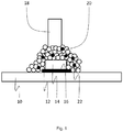
- Fig. 1 shows a schematic view illustrating the method according to the invention.
- Fig. 1 illustrates a method of connecting two components by ultrasonic welding in the field of power semiconductor module production.
- a substrate 10 is shown on which substrate 10 a metallization 12 is provided.
- a terminal 14 is shown which shall be welded to the metallization 12.
- the terminal 14 and the substrate 12 comprising the metallization 14 are aligned to form a welding interface 16.
- a welding tool 18, such as a sonotrode is aligned and may come in contact to the terminal 14. In order to perform the welding process, the sonotrode may be activated.
- a trapping material 20 is shown, which is removably arranged such, that it at least partly encompasses the welding interface 16.
- the trapping material 20 may thereby be arranged before or after aligning the terminal 14 and the substrate 10 with the metallization 12.
- the trapping material 20 is a foam, such as a fluid based foam or a solid foam, but could also be a gel or a textile.
- the trapping material 20 is a foam or a textile the pockets of the foam or pores of the textile may be filled filled with an inert gas or with a surfactant chemistries.
- the density and/or viscosity of the foam may easily be adjusted by altering the quantity and material with all or one or two major constituents, e.g a solid and/or liquid and/or gas forming the foam.
- the foam may further be a single foam unit or multiple linked cell units.
- a single foam unit shall thereby mean for example one big bubble, whereas multiple linked cells shall mean lots of smaller bubbles that forms a denser foam material like in a shaving foam.
- trapping material 20 could be locally around the welding region or all over the substrate baseplate assembly or introduced as a chamber filled with trapping material 20.
- the free area for the application of the trapping material 20 may thus be all or partly around the joining partners.
- the trapping material 20 may prevent particles 22 which are ejected out of the welding region due to welding forces to contaminate the surrounding of the components to be welded.
- the welding process may be performed at a temperature lying in the range of ⁇ 10°C to ⁇ 80°C.
- the critical hot and fast particles 20 of sizes from typically nano to micrometer ranges can be easily trapped by the trapping material 20 due to its cooling capability and suitable surface tension to entrap particles 20 from all possible directions.
- a cleaning procedure may be performed after the welding step.
- an easy or reasonable post cleaning or/and post suction process may be performed and potentially followed by post baking.
- Post cleaning chemistry could involve defoaming chemistries for efficient cleaning and regeneration of cleaning chemistries.
- At least one surface for example a plurality of surfaces or the whole of the surfaces, such as the whole of the power semiconductor device is pretreated by a surface tension lowering material.
- the respective surface may be coated with the respective material.
- the particles 20 on the welding tool 18 may or may not be cleaned depending on the choice of particle trapping material 20.
- the method may be performed at a pressure lying in the range of ⁇ 1mbar to ⁇ 6bar. Additionally or alternatively, the method may be performed under an atmosphere comprising an inert gas.
- the components to be welded i.e. the terminal 14 and the substrate 10, or its metallization 12, respectively, can further be designed in such a way that particles deposited in the trapping material 20 do not affect the operational properties of the product.
- particles deposited in the trapping material 20 do not affect the operational properties of the product.
- this could e.g. be achieved by metal surfaces of the components region covered by the trapping material 20
Landscapes
- Engineering & Computer Science (AREA)
- Mechanical Engineering (AREA)
- Physics & Mathematics (AREA)
- Health & Medical Sciences (AREA)
- Oral & Maxillofacial Surgery (AREA)
- Thermal Sciences (AREA)
- Optics & Photonics (AREA)
- Pressure Welding/Diffusion-Bonding (AREA)
- Wire Bonding (AREA)
- Lining Or Joining Of Plastics Or The Like (AREA)
- Electric Connection Of Electric Components To Printed Circuits (AREA)
Priority Applications (1)
| Application Number | Priority Date | Filing Date | Title |
|---|---|---|---|
| EP14720125.5A EP3046717B1 (en) | 2013-09-17 | 2014-04-28 | Method for ultrasonic welding with particles trapping |
Applications Claiming Priority (3)
| Application Number | Priority Date | Filing Date | Title |
|---|---|---|---|
| EP13184769 | 2013-09-17 | ||
| PCT/EP2014/058604 WO2015039771A1 (en) | 2013-09-17 | 2014-04-28 | Method for ultrasonic welding with particles trapping |
| EP14720125.5A EP3046717B1 (en) | 2013-09-17 | 2014-04-28 | Method for ultrasonic welding with particles trapping |
Publications (2)
| Publication Number | Publication Date |
|---|---|
| EP3046717A1 EP3046717A1 (en) | 2016-07-27 |
| EP3046717B1 true EP3046717B1 (en) | 2019-12-11 |
Family
ID=49165665
Family Applications (1)
| Application Number | Title | Priority Date | Filing Date |
|---|---|---|---|
| EP14720125.5A Active EP3046717B1 (en) | 2013-09-17 | 2014-04-28 | Method for ultrasonic welding with particles trapping |
Country Status (6)
| Country | Link |
|---|---|
| US (1) | US9975194B2 (enExample) |
| EP (1) | EP3046717B1 (enExample) |
| JP (1) | JP6718819B2 (enExample) |
| KR (1) | KR102147561B1 (enExample) |
| CN (1) | CN105531068B (enExample) |
| WO (1) | WO2015039771A1 (enExample) |
Families Citing this family (3)
| Publication number | Priority date | Publication date | Assignee | Title |
|---|---|---|---|---|
| EP3613075B1 (en) * | 2017-05-02 | 2020-11-18 | ABB Schweiz AG | Resin encapsulated power semiconductor module with exposed terminal areas |
| JP7608749B2 (ja) * | 2020-08-20 | 2025-01-07 | 株式会社大林組 | 作業方法及び泡状体製造装置 |
| KR102376232B1 (ko) * | 2020-10-28 | 2022-03-17 | 동명대학교 산학협력단 | 초음파 용접 방법 |
Family Cites Families (43)
| Publication number | Priority date | Publication date | Assignee | Title |
|---|---|---|---|---|
| US3393102A (en) | 1965-01-15 | 1968-07-16 | Lincoln Electric Co | Arc welding flux |
| US3586122A (en) * | 1970-04-27 | 1971-06-22 | Branson Instr | Sonic apparatus with sonic energy barrier means |
| JPS5357481A (en) * | 1976-11-04 | 1978-05-24 | Canon Inc | Connecting process |
| KR900003157B1 (ko) * | 1986-04-02 | 1990-05-09 | 가부시끼가이샤 히다찌세이샤꾸쇼 | 스루호울 도금의 전처리 방법 |
| US4770730A (en) * | 1987-09-29 | 1988-09-13 | Tachi-S. Co., Ltd. | Ultrasonic welding method for soft elastic foam body |
| JPH02105513A (ja) * | 1988-10-14 | 1990-04-18 | Nec Corp | ヒューズ付きチップ状固体電解コンデンサ |
| JP2564415B2 (ja) * | 1990-04-18 | 1996-12-18 | 株式会社日立製作所 | 空気流量検出器 |
| US5239806A (en) * | 1990-11-02 | 1993-08-31 | Ak Technology, Inc. | Thermoplastic semiconductor package and method of producing it |
| JP2662131B2 (ja) * | 1991-12-26 | 1997-10-08 | 松下電器産業株式会社 | ボンディング装置 |
| CA2117685C (en) * | 1992-04-10 | 1999-06-01 | William J. Hendershot | A method of ultrasonically welding articles of porous polytetrafluoroethylene |
| DE69431023T2 (de) * | 1993-09-01 | 2003-02-06 | Kabushiki Kaisha Toshiba, Kawasaki | Halbleiteraufbau und Verfahren zur Herstellung |
| JP3297254B2 (ja) * | 1995-07-05 | 2002-07-02 | 株式会社東芝 | 半導体パッケージおよびその製造方法 |
| KR100438256B1 (ko) * | 1995-12-18 | 2004-08-25 | 마츠시타 덴끼 산교 가부시키가이샤 | 반도체장치 및 그 제조방법 |
| JP3610999B2 (ja) * | 1996-06-07 | 2005-01-19 | 松下電器産業株式会社 | 半導体素子の実装方法 |
| US5926694A (en) * | 1996-07-11 | 1999-07-20 | Pfu Limited | Semiconductor device and a manufacturing method thereof |
| JP2924830B2 (ja) * | 1996-11-15 | 1999-07-26 | 日本電気株式会社 | 半導体装置及びその製造方法 |
| JP3233059B2 (ja) * | 1997-03-07 | 2001-11-26 | 株式会社村田製作所 | 超音波センサ |
| US6077382A (en) * | 1997-05-09 | 2000-06-20 | Citizen Watch Co., Ltd | Mounting method of semiconductor chip |
| US5969461A (en) * | 1998-04-08 | 1999-10-19 | Cts Corporation | Surface acoustic wave device package and method |
| JP2000068327A (ja) * | 1998-08-20 | 2000-03-03 | Matsushita Electric Ind Co Ltd | 部品の実装方法と装置 |
| KR20000057810A (ko) * | 1999-01-28 | 2000-09-25 | 가나이 쓰토무 | 반도체 장치 |
| JP4338834B2 (ja) | 1999-08-06 | 2009-10-07 | 日本テキサス・インスツルメンツ株式会社 | 超音波振動を用いた半導体チップの実装方法 |
| JP4592845B2 (ja) * | 1999-09-21 | 2010-12-08 | パナソニック株式会社 | 電池 |
| JP4564118B2 (ja) * | 1999-10-26 | 2010-10-20 | パナソニック株式会社 | 電池及びその製造方法 |
| JP2001178839A (ja) * | 1999-12-27 | 2001-07-03 | Taiho Ind Co Ltd | 高熱粉粒体の処理方法 |
| JP2001308145A (ja) * | 2000-04-25 | 2001-11-02 | Fujitsu Ltd | 半導体チップの実装方法 |
| JPWO2002039180A1 (ja) * | 2000-11-10 | 2004-03-18 | 株式会社村上開明堂 | 固体型エレクトロクロミック素子及びその素子を用いたミラー装置並びにcrtディスプレイ |
| JP3988878B2 (ja) * | 2001-03-02 | 2007-10-10 | 東レエンジニアリング株式会社 | チップ実装方法およびその装置 |
| JP4199460B2 (ja) * | 2002-01-23 | 2008-12-17 | パナソニック株式会社 | 角形密閉式電池 |
| US20060091184A1 (en) * | 2004-10-28 | 2006-05-04 | Art Bayot | Method of mitigating voids during solder reflow |
| US20090133803A1 (en) * | 2006-02-10 | 2009-05-28 | Sca Hygiene Products Ab | Device and Means of Processing a Material by Means of an Ultrasonic Device |
| JP2006186401A (ja) * | 2006-03-30 | 2006-07-13 | Denso Corp | 半導体装置及び半導体装置の製造方法 |
| JP2006186402A (ja) * | 2006-03-30 | 2006-07-13 | Denso Corp | 半導体装置及び半導体装置の製造方法 |
| US20080060741A1 (en) * | 2006-09-07 | 2008-03-13 | Privitera Marc P | Ultrasonically Bonded Nonwoven Permeable Pouch |
| KR100874925B1 (ko) * | 2007-06-04 | 2008-12-19 | 삼성전자주식회사 | 반도체 패키지, 그 제조 방법, 이를 포함하는 카드 및 이를포함하는 시스템 |
| WO2009031996A2 (en) * | 2007-09-06 | 2009-03-12 | Tyco Healthcare Group Lp | Touchless auto-drop sharps container |
| US20100084748A1 (en) * | 2008-06-04 | 2010-04-08 | National Semiconductor Corporation | Thin foil for use in packaging integrated circuits |
| FR2934609B1 (fr) * | 2008-07-30 | 2011-07-22 | Jet Metal Technologies | Procede non eletrolytique de metallisation en ligne de substrats par projection avec traitement de surface prealable et dispositif pour la mise en oeuvre du procede. |
| JP2010040615A (ja) * | 2008-08-01 | 2010-02-18 | Hitachi Ltd | 半導体装置 |
| CN102123811A (zh) * | 2008-08-14 | 2011-07-13 | 日立金属株式会社 | 熔融金属供给筒、内置了该供给筒的熔融金属供给装置和熔融金属供给方法 |
| WO2014000975A1 (en) | 2012-06-26 | 2014-01-03 | Abb Technology Ag | Device and method for ultrasonic welding |
| CN102800833B (zh) * | 2012-08-31 | 2015-03-18 | 江苏宏微科技股份有限公司 | 功率模块电极端子及其焊接方法 |
| CN103143832A (zh) * | 2013-02-26 | 2013-06-12 | 芜湖新宝超声波设备有限公司 | 一种超声波焊接机 |
-
2014
- 2014-04-28 CN CN201480051289.8A patent/CN105531068B/zh active Active
- 2014-04-28 JP JP2016543334A patent/JP6718819B2/ja active Active
- 2014-04-28 KR KR1020167007050A patent/KR102147561B1/ko active Active
- 2014-04-28 WO PCT/EP2014/058604 patent/WO2015039771A1/en not_active Ceased
- 2014-04-28 EP EP14720125.5A patent/EP3046717B1/en active Active
-
2016
- 2016-03-11 US US15/067,779 patent/US9975194B2/en active Active
Non-Patent Citations (1)
| Title |
|---|
| None * |
Also Published As
| Publication number | Publication date |
|---|---|
| JP6718819B2 (ja) | 2020-07-08 |
| KR102147561B1 (ko) | 2020-08-25 |
| CN105531068A (zh) | 2016-04-27 |
| US20160193678A1 (en) | 2016-07-07 |
| US9975194B2 (en) | 2018-05-22 |
| WO2015039771A1 (en) | 2015-03-26 |
| JP2016533040A (ja) | 2016-10-20 |
| EP3046717A1 (en) | 2016-07-27 |
| KR20160054491A (ko) | 2016-05-16 |
| CN105531068B (zh) | 2018-11-23 |
Similar Documents
| Publication | Publication Date | Title |
|---|---|---|
| KR101445118B1 (ko) | 세정 화합물 및 그 세정 화합물을 이용하는 방법 및 시스템 | |
| KR101547000B1 (ko) | 다중 스테이지 기판 세정 방법 및 장치 | |
| EP3046717B1 (en) | Method for ultrasonic welding with particles trapping | |
| US20020182782A1 (en) | Stereolithographic methods for fabricating hermetic semiconductor device packages and semiconductor devices including stereolithographically fabricated hermetic packages | |
| KR20120048562A (ko) | 진보된 기판 세정을 위한 재료 및 시스템 | |
| KR20080083196A (ko) | 기판으로부터 오염물질을 제거하기 위한 방법 및 장치 | |
| EP1620883A1 (en) | Laser machining using an active assist gas | |
| KR20070072374A (ko) | 기판으로부터 오염물질을 제거하는 방법 및 세척 용액을만드는 방법 | |
| JP2025031776A (ja) | 接合システムおよび接合方法 | |
| CN103065987A (zh) | 芯片接合装置及芯片接合方法 | |
| US12087728B2 (en) | Systems and methods related to wire bond cleaning and wire bonding recovery | |
| CN113140506A (zh) | 热压结合器、及其操作方法、和密脚距倒装芯片组件的互连方法 | |
| CN102989720A (zh) | 一种激光辅助清除基体表面纳米颗粒的方法和装置 | |
| JP4956551B2 (ja) | 基板から汚染を除去するための方法および装置 | |
| JP2012086301A (ja) | 半導体製造装置、及び半導体製造方法 | |
| WO2014000975A1 (en) | Device and method for ultrasonic welding | |
| EP2848353A1 (en) | Method for ultrasonic welding with particles trapping | |
| CN107611008A (zh) | 一种用于清除基板及其上的芯片表面的助焊剂的方法 | |
| Albalak | Dicing MEMS | |
| KR101153134B1 (ko) | 와이어 본딩 공정의 캐필러리 클리닝 방법 | |
| CN106328487B (zh) | 功率二极管装置的处理方法及设备 | |
| JP2017168508A (ja) | 除去方法および製造方法 | |
| JP2006326801A (ja) | 切屑除去方法 | |
| Benjamin et al. | Yield and reliability in flip chip underfill for optical modules | |
| Roemer et al. | Laser micro-machining of hydrophobic-hydrophilic patterns for fluid driven self-alignment in micro-assembly |
Legal Events
| Date | Code | Title | Description |
|---|---|---|---|
| PUAI | Public reference made under article 153(3) epc to a published international application that has entered the european phase |
Free format text: ORIGINAL CODE: 0009012 |
|
| 17P | Request for examination filed |
Effective date: 20160203 |
|
| AK | Designated contracting states |
Kind code of ref document: A1 Designated state(s): AL AT BE BG CH CY CZ DE DK EE ES FI FR GB GR HR HU IE IS IT LI LT LU LV MC MK MT NL NO PL PT RO RS SE SI SK SM TR |
|
| AX | Request for extension of the european patent |
Extension state: BA ME |
|
| DAX | Request for extension of the european patent (deleted) | ||
| RAP1 | Party data changed (applicant data changed or rights of an application transferred) |
Owner name: ABB SCHWEIZ AG |
|
| GRAP | Despatch of communication of intention to grant a patent |
Free format text: ORIGINAL CODE: EPIDOSNIGR1 |
|
| STAA | Information on the status of an ep patent application or granted ep patent |
Free format text: STATUS: GRANT OF PATENT IS INTENDED |
|
| INTG | Intention to grant announced |
Effective date: 20190701 |
|
| GRAS | Grant fee paid |
Free format text: ORIGINAL CODE: EPIDOSNIGR3 |
|
| GRAA | (expected) grant |
Free format text: ORIGINAL CODE: 0009210 |
|
| STAA | Information on the status of an ep patent application or granted ep patent |
Free format text: STATUS: THE PATENT HAS BEEN GRANTED |
|
| AK | Designated contracting states |
Kind code of ref document: B1 Designated state(s): AL AT BE BG CH CY CZ DE DK EE ES FI FR GB GR HR HU IE IS IT LI LT LU LV MC MK MT NL NO PL PT RO RS SE SI SK SM TR |
|
| REG | Reference to a national code |
Ref country code: GB Ref legal event code: FG4D |
|
| REG | Reference to a national code |
Ref country code: CH Ref legal event code: EP |
|
| REG | Reference to a national code |
Ref country code: AT Ref legal event code: REF Ref document number: 1211714 Country of ref document: AT Kind code of ref document: T Effective date: 20191215 |
|
| REG | Reference to a national code |
Ref country code: DE Ref legal event code: R096 Ref document number: 602014058195 Country of ref document: DE |
|
| REG | Reference to a national code |
Ref country code: IE Ref legal event code: FG4D |
|
| REG | Reference to a national code |
Ref country code: NL Ref legal event code: MP Effective date: 20191211 |
|
| REG | Reference to a national code |
Ref country code: LT Ref legal event code: MG4D |
|
| PG25 | Lapsed in a contracting state [announced via postgrant information from national office to epo] |
Ref country code: GR Free format text: LAPSE BECAUSE OF FAILURE TO SUBMIT A TRANSLATION OF THE DESCRIPTION OR TO PAY THE FEE WITHIN THE PRESCRIBED TIME-LIMIT Effective date: 20200312 Ref country code: NO Free format text: LAPSE BECAUSE OF FAILURE TO SUBMIT A TRANSLATION OF THE DESCRIPTION OR TO PAY THE FEE WITHIN THE PRESCRIBED TIME-LIMIT Effective date: 20200311 Ref country code: LT Free format text: LAPSE BECAUSE OF FAILURE TO SUBMIT A TRANSLATION OF THE DESCRIPTION OR TO PAY THE FEE WITHIN THE PRESCRIBED TIME-LIMIT Effective date: 20191211 Ref country code: SE Free format text: LAPSE BECAUSE OF FAILURE TO SUBMIT A TRANSLATION OF THE DESCRIPTION OR TO PAY THE FEE WITHIN THE PRESCRIBED TIME-LIMIT Effective date: 20191211 Ref country code: LV Free format text: LAPSE BECAUSE OF FAILURE TO SUBMIT A TRANSLATION OF THE DESCRIPTION OR TO PAY THE FEE WITHIN THE PRESCRIBED TIME-LIMIT Effective date: 20191211 Ref country code: FI Free format text: LAPSE BECAUSE OF FAILURE TO SUBMIT A TRANSLATION OF THE DESCRIPTION OR TO PAY THE FEE WITHIN THE PRESCRIBED TIME-LIMIT Effective date: 20191211 Ref country code: BG Free format text: LAPSE BECAUSE OF FAILURE TO SUBMIT A TRANSLATION OF THE DESCRIPTION OR TO PAY THE FEE WITHIN THE PRESCRIBED TIME-LIMIT Effective date: 20200311 |
|
| PG25 | Lapsed in a contracting state [announced via postgrant information from national office to epo] |
Ref country code: RS Free format text: LAPSE BECAUSE OF FAILURE TO SUBMIT A TRANSLATION OF THE DESCRIPTION OR TO PAY THE FEE WITHIN THE PRESCRIBED TIME-LIMIT Effective date: 20191211 Ref country code: HR Free format text: LAPSE BECAUSE OF FAILURE TO SUBMIT A TRANSLATION OF THE DESCRIPTION OR TO PAY THE FEE WITHIN THE PRESCRIBED TIME-LIMIT Effective date: 20191211 |
|
| PG25 | Lapsed in a contracting state [announced via postgrant information from national office to epo] |
Ref country code: AL Free format text: LAPSE BECAUSE OF FAILURE TO SUBMIT A TRANSLATION OF THE DESCRIPTION OR TO PAY THE FEE WITHIN THE PRESCRIBED TIME-LIMIT Effective date: 20191211 |
|
| PG25 | Lapsed in a contracting state [announced via postgrant information from national office to epo] |
Ref country code: ES Free format text: LAPSE BECAUSE OF FAILURE TO SUBMIT A TRANSLATION OF THE DESCRIPTION OR TO PAY THE FEE WITHIN THE PRESCRIBED TIME-LIMIT Effective date: 20191211 Ref country code: PT Free format text: LAPSE BECAUSE OF FAILURE TO SUBMIT A TRANSLATION OF THE DESCRIPTION OR TO PAY THE FEE WITHIN THE PRESCRIBED TIME-LIMIT Effective date: 20200506 Ref country code: EE Free format text: LAPSE BECAUSE OF FAILURE TO SUBMIT A TRANSLATION OF THE DESCRIPTION OR TO PAY THE FEE WITHIN THE PRESCRIBED TIME-LIMIT Effective date: 20191211 Ref country code: NL Free format text: LAPSE BECAUSE OF FAILURE TO SUBMIT A TRANSLATION OF THE DESCRIPTION OR TO PAY THE FEE WITHIN THE PRESCRIBED TIME-LIMIT Effective date: 20191211 Ref country code: CZ Free format text: LAPSE BECAUSE OF FAILURE TO SUBMIT A TRANSLATION OF THE DESCRIPTION OR TO PAY THE FEE WITHIN THE PRESCRIBED TIME-LIMIT Effective date: 20191211 Ref country code: RO Free format text: LAPSE BECAUSE OF FAILURE TO SUBMIT A TRANSLATION OF THE DESCRIPTION OR TO PAY THE FEE WITHIN THE PRESCRIBED TIME-LIMIT Effective date: 20191211 |
|
| PG25 | Lapsed in a contracting state [announced via postgrant information from national office to epo] |
Ref country code: SK Free format text: LAPSE BECAUSE OF FAILURE TO SUBMIT A TRANSLATION OF THE DESCRIPTION OR TO PAY THE FEE WITHIN THE PRESCRIBED TIME-LIMIT Effective date: 20191211 Ref country code: IS Free format text: LAPSE BECAUSE OF FAILURE TO SUBMIT A TRANSLATION OF THE DESCRIPTION OR TO PAY THE FEE WITHIN THE PRESCRIBED TIME-LIMIT Effective date: 20200411 Ref country code: SM Free format text: LAPSE BECAUSE OF FAILURE TO SUBMIT A TRANSLATION OF THE DESCRIPTION OR TO PAY THE FEE WITHIN THE PRESCRIBED TIME-LIMIT Effective date: 20191211 |
|
| REG | Reference to a national code |
Ref country code: DE Ref legal event code: R097 Ref document number: 602014058195 Country of ref document: DE |
|
| REG | Reference to a national code |
Ref country code: AT Ref legal event code: MK05 Ref document number: 1211714 Country of ref document: AT Kind code of ref document: T Effective date: 20191211 |
|
| PLBE | No opposition filed within time limit |
Free format text: ORIGINAL CODE: 0009261 |
|
| STAA | Information on the status of an ep patent application or granted ep patent |
Free format text: STATUS: NO OPPOSITION FILED WITHIN TIME LIMIT |
|
| PG25 | Lapsed in a contracting state [announced via postgrant information from national office to epo] |
Ref country code: DK Free format text: LAPSE BECAUSE OF FAILURE TO SUBMIT A TRANSLATION OF THE DESCRIPTION OR TO PAY THE FEE WITHIN THE PRESCRIBED TIME-LIMIT Effective date: 20191211 |
|
| 26N | No opposition filed |
Effective date: 20200914 |
|
| PG25 | Lapsed in a contracting state [announced via postgrant information from national office to epo] |
Ref country code: AT Free format text: LAPSE BECAUSE OF FAILURE TO SUBMIT A TRANSLATION OF THE DESCRIPTION OR TO PAY THE FEE WITHIN THE PRESCRIBED TIME-LIMIT Effective date: 20191211 Ref country code: MC Free format text: LAPSE BECAUSE OF FAILURE TO SUBMIT A TRANSLATION OF THE DESCRIPTION OR TO PAY THE FEE WITHIN THE PRESCRIBED TIME-LIMIT Effective date: 20191211 Ref country code: PL Free format text: LAPSE BECAUSE OF FAILURE TO SUBMIT A TRANSLATION OF THE DESCRIPTION OR TO PAY THE FEE WITHIN THE PRESCRIBED TIME-LIMIT Effective date: 20191211 Ref country code: SI Free format text: LAPSE BECAUSE OF FAILURE TO SUBMIT A TRANSLATION OF THE DESCRIPTION OR TO PAY THE FEE WITHIN THE PRESCRIBED TIME-LIMIT Effective date: 20191211 |
|
| REG | Reference to a national code |
Ref country code: CH Ref legal event code: PL |
|
| PG25 | Lapsed in a contracting state [announced via postgrant information from national office to epo] |
Ref country code: CH Free format text: LAPSE BECAUSE OF NON-PAYMENT OF DUE FEES Effective date: 20200430 Ref country code: LI Free format text: LAPSE BECAUSE OF NON-PAYMENT OF DUE FEES Effective date: 20200430 Ref country code: FR Free format text: LAPSE BECAUSE OF NON-PAYMENT OF DUE FEES Effective date: 20200430 Ref country code: LU Free format text: LAPSE BECAUSE OF NON-PAYMENT OF DUE FEES Effective date: 20200428 Ref country code: IT Free format text: LAPSE BECAUSE OF FAILURE TO SUBMIT A TRANSLATION OF THE DESCRIPTION OR TO PAY THE FEE WITHIN THE PRESCRIBED TIME-LIMIT Effective date: 20191211 |
|
| REG | Reference to a national code |
Ref country code: BE Ref legal event code: MM Effective date: 20200430 |
|
| PG25 | Lapsed in a contracting state [announced via postgrant information from national office to epo] |
Ref country code: BE Free format text: LAPSE BECAUSE OF NON-PAYMENT OF DUE FEES Effective date: 20200430 |
|
| PG25 | Lapsed in a contracting state [announced via postgrant information from national office to epo] |
Ref country code: IE Free format text: LAPSE BECAUSE OF NON-PAYMENT OF DUE FEES Effective date: 20200428 |
|
| REG | Reference to a national code |
Ref country code: DE Ref legal event code: R081 Ref document number: 602014058195 Country of ref document: DE Owner name: HITACHI ENERGY SWITZERLAND AG, CH Free format text: FORMER OWNER: ABB SCHWEIZ AG, BADEN, CH Ref country code: DE Ref legal event code: R082 Ref document number: 602014058195 Country of ref document: DE Representative=s name: DENNEMEYER & ASSOCIATES RECHTSANWALTSGESELLSCH, DE Ref country code: DE Ref legal event code: R081 Ref document number: 602014058195 Country of ref document: DE Owner name: HITACHI ENERGY LTD, CH Free format text: FORMER OWNER: ABB SCHWEIZ AG, BADEN, CH Ref country code: DE Ref legal event code: R082 Ref document number: 602014058195 Country of ref document: DE Representative=s name: DENNEMEYER & ASSOCIATES S.A., DE Ref country code: DE Ref legal event code: R081 Ref document number: 602014058195 Country of ref document: DE Owner name: ABB POWER GRIDS SWITZERLAND AG, CH Free format text: FORMER OWNER: ABB SCHWEIZ AG, BADEN, CH |
|
| REG | Reference to a national code |
Ref country code: GB Ref legal event code: 732E Free format text: REGISTERED BETWEEN 20211104 AND 20211110 |
|
| PG25 | Lapsed in a contracting state [announced via postgrant information from national office to epo] |
Ref country code: TR Free format text: LAPSE BECAUSE OF FAILURE TO SUBMIT A TRANSLATION OF THE DESCRIPTION OR TO PAY THE FEE WITHIN THE PRESCRIBED TIME-LIMIT Effective date: 20191211 Ref country code: MT Free format text: LAPSE BECAUSE OF FAILURE TO SUBMIT A TRANSLATION OF THE DESCRIPTION OR TO PAY THE FEE WITHIN THE PRESCRIBED TIME-LIMIT Effective date: 20191211 Ref country code: CY Free format text: LAPSE BECAUSE OF FAILURE TO SUBMIT A TRANSLATION OF THE DESCRIPTION OR TO PAY THE FEE WITHIN THE PRESCRIBED TIME-LIMIT Effective date: 20191211 |
|
| REG | Reference to a national code |
Ref country code: DE Ref legal event code: R081 Ref document number: 602014058195 Country of ref document: DE Owner name: HITACHI ENERGY SWITZERLAND AG, CH Free format text: FORMER OWNER: ABB POWER GRIDS SWITZERLAND AG, BADEN, CH Ref country code: DE Ref legal event code: R081 Ref document number: 602014058195 Country of ref document: DE Owner name: HITACHI ENERGY LTD, CH Free format text: FORMER OWNER: ABB POWER GRIDS SWITZERLAND AG, BADEN, CH |
|
| PG25 | Lapsed in a contracting state [announced via postgrant information from national office to epo] |
Ref country code: MK Free format text: LAPSE BECAUSE OF FAILURE TO SUBMIT A TRANSLATION OF THE DESCRIPTION OR TO PAY THE FEE WITHIN THE PRESCRIBED TIME-LIMIT Effective date: 20191211 |
|
| P01 | Opt-out of the competence of the unified patent court (upc) registered |
Effective date: 20230527 |
|
| REG | Reference to a national code |
Ref country code: DE Ref legal event code: R082 Ref document number: 602014058195 Country of ref document: DE Representative=s name: DENNEMEYER & ASSOCIATES RECHTSANWALTSGESELLSCH, DE Ref country code: DE Ref legal event code: R082 Ref document number: 602014058195 Country of ref document: DE Representative=s name: DENNEMEYER & ASSOCIATES S.A., DE Ref country code: DE Ref legal event code: R081 Ref document number: 602014058195 Country of ref document: DE Owner name: HITACHI ENERGY LTD, CH Free format text: FORMER OWNER: HITACHI ENERGY SWITZERLAND AG, BADEN, CH |
|
| REG | Reference to a national code |
Ref country code: GB Ref legal event code: 732E Free format text: REGISTERED BETWEEN 20240718 AND 20240724 |
|
| REG | Reference to a national code |
Ref country code: DE Ref legal event code: R082 Ref document number: 602014058195 Country of ref document: DE Representative=s name: DENNEMEYER & ASSOCIATES RECHTSANWALTSGESELLSCH, DE |
|
| PGFP | Annual fee paid to national office [announced via postgrant information from national office to epo] |
Ref country code: DE Payment date: 20250422 Year of fee payment: 12 |
|
| PGFP | Annual fee paid to national office [announced via postgrant information from national office to epo] |
Ref country code: GB Payment date: 20250423 Year of fee payment: 12 |