EP3043398B1 - Matériaux et dispositifs électroluminescents organiques - Google Patents
Matériaux et dispositifs électroluminescents organiques Download PDFInfo
- Publication number
- EP3043398B1 EP3043398B1 EP15202033.5A EP15202033A EP3043398B1 EP 3043398 B1 EP3043398 B1 EP 3043398B1 EP 15202033 A EP15202033 A EP 15202033A EP 3043398 B1 EP3043398 B1 EP 3043398B1
- Authority
- EP
- European Patent Office
- Prior art keywords
- compound
- group
- substitution
- combinations
- biphenyl
- Prior art date
- Legal status (The legal status is an assumption and is not a legal conclusion. Google has not performed a legal analysis and makes no representation as to the accuracy of the status listed.)
- Active
Links
- 239000000463 material Substances 0.000 title claims description 97
- 150000001875 compounds Chemical class 0.000 claims description 149
- UHOVQNZJYSORNB-UHFFFAOYSA-N Benzene Chemical compound C1=CC=CC=C1 UHOVQNZJYSORNB-UHFFFAOYSA-N 0.000 claims description 102
- JUJWROOIHBZHMG-UHFFFAOYSA-N Pyridine Chemical compound C1=CC=NC=C1 JUJWROOIHBZHMG-UHFFFAOYSA-N 0.000 claims description 90
- ZUOUZKKEUPVFJK-UHFFFAOYSA-N diphenyl Chemical compound C1=CC=CC=C1C1=CC=CC=C1 ZUOUZKKEUPVFJK-UHFFFAOYSA-N 0.000 claims description 88
- 239000010410 layer Substances 0.000 claims description 85
- -1 2-ethylhexyl Chemical group 0.000 claims description 63
- 238000006467 substitution reaction Methods 0.000 claims description 56
- 239000000203 mixture Substances 0.000 claims description 53
- 125000000217 alkyl group Chemical group 0.000 claims description 46
- UMJSCPRVCHMLSP-UHFFFAOYSA-N pyridine Natural products COC1=CC=CN=C1 UMJSCPRVCHMLSP-UHFFFAOYSA-N 0.000 claims description 45
- 239000004305 biphenyl Substances 0.000 claims description 44
- 235000010290 biphenyl Nutrition 0.000 claims description 44
- 125000000753 cycloalkyl group Chemical group 0.000 claims description 44
- 125000001424 substituent group Chemical group 0.000 claims description 43
- 239000012044 organic layer Substances 0.000 claims description 41
- YZCKVEUIGOORGS-OUBTZVSYSA-N Deuterium Chemical group [2H] YZCKVEUIGOORGS-OUBTZVSYSA-N 0.000 claims description 40
- 229910052805 deuterium Inorganic materials 0.000 claims description 40
- IYYZUPMFVPLQIF-UHFFFAOYSA-N dibenzothiophene Chemical compound C1=CC=C2C3=CC=CC=C3SC2=C1 IYYZUPMFVPLQIF-UHFFFAOYSA-N 0.000 claims description 39
- YJTKZCDBKVTVBY-UHFFFAOYSA-N 1,3-Diphenylbenzene Chemical group C1=CC=CC=C1C1=CC=CC(C=2C=CC=CC=2)=C1 YJTKZCDBKVTVBY-UHFFFAOYSA-N 0.000 claims description 37
- 125000003545 alkoxy group Chemical group 0.000 claims description 37
- 150000002825 nitriles Chemical class 0.000 claims description 37
- NIHNNTQXNPWCJQ-UHFFFAOYSA-N fluorene Chemical compound C1=CC=C2CC3=CC=CC=C3C2=C1 NIHNNTQXNPWCJQ-UHFFFAOYSA-N 0.000 claims description 36
- 125000003118 aryl group Chemical group 0.000 claims description 33
- TXCDCPKCNAJMEE-UHFFFAOYSA-N dibenzofuran Chemical compound C1=CC=C2C3=CC=CC=C3OC2=C1 TXCDCPKCNAJMEE-UHFFFAOYSA-N 0.000 claims description 33
- 229910052736 halogen Inorganic materials 0.000 claims description 33
- 150000002367 halogens Chemical class 0.000 claims description 33
- 125000001072 heteroaryl group Chemical group 0.000 claims description 32
- 229910052739 hydrogen Inorganic materials 0.000 claims description 31
- 239000001257 hydrogen Substances 0.000 claims description 31
- 150000002431 hydrogen Chemical group 0.000 claims description 30
- 239000003446 ligand Substances 0.000 claims description 27
- 125000000449 nitro group Chemical group [O-][N+](*)=O 0.000 claims description 25
- 125000001181 organosilyl group Chemical group [SiH3]* 0.000 claims description 25
- 238000000151 deposition Methods 0.000 claims description 23
- UFWIBTONFRDIAS-UHFFFAOYSA-N Naphthalene Chemical compound C1=CC=CC2=CC=CC=C21 UFWIBTONFRDIAS-UHFFFAOYSA-N 0.000 claims description 22
- 238000000034 method Methods 0.000 claims description 22
- 229910052760 oxygen Inorganic materials 0.000 claims description 22
- 239000002019 doping agent Substances 0.000 claims description 21
- SMWDFEZZVXVKRB-UHFFFAOYSA-N Quinoline Chemical compound N1=CC=CC2=CC=CC=C21 SMWDFEZZVXVKRB-UHFFFAOYSA-N 0.000 claims description 20
- 229940125782 compound 2 Drugs 0.000 claims description 20
- 229910052717 sulfur Inorganic materials 0.000 claims description 20
- UJOBWOGCFQCDNV-UHFFFAOYSA-N 9H-carbazole Chemical compound C1=CC=C2C3=CC=CC=C3NC2=C1 UJOBWOGCFQCDNV-UHFFFAOYSA-N 0.000 claims description 18
- AWJUIBRHMBBTKR-UHFFFAOYSA-N isoquinoline Chemical compound C1=NC=CC2=CC=CC=C21 AWJUIBRHMBBTKR-UHFFFAOYSA-N 0.000 claims description 18
- YNPNZTXNASCQKK-UHFFFAOYSA-N phenanthrene Chemical compound C1=CC=C2C3=CC=CC=C3C=CC2=C1 YNPNZTXNASCQKK-UHFFFAOYSA-N 0.000 claims description 18
- 125000003342 alkenyl group Chemical group 0.000 claims description 16
- 125000003710 aryl alkyl group Chemical group 0.000 claims description 16
- 125000000304 alkynyl group Chemical group 0.000 claims description 15
- 230000000903 blocking effect Effects 0.000 claims description 15
- DHFABSXGNHDNCO-UHFFFAOYSA-N dibenzoselenophene Chemical compound C1=CC=C2C3=CC=CC=C3[se]C2=C1 DHFABSXGNHDNCO-UHFFFAOYSA-N 0.000 claims description 15
- 125000001997 phenyl group Chemical group [H]C1=C([H])C([H])=C(*)C([H])=C1[H] 0.000 claims description 15
- 229910052711 selenium Inorganic materials 0.000 claims description 15
- 125000000392 cycloalkenyl group Chemical group 0.000 claims description 14
- 239000000758 substrate Substances 0.000 claims description 13
- 125000002252 acyl group Chemical group 0.000 claims description 12
- 125000004104 aryloxy group Chemical group 0.000 claims description 12
- 125000002915 carbonyl group Chemical group [*:2]C([*:1])=O 0.000 claims description 12
- 150000002148 esters Chemical class 0.000 claims description 12
- 125000004404 heteroalkyl group Chemical group 0.000 claims description 12
- 150000002527 isonitriles Chemical class 0.000 claims description 12
- FVZVCSNXTFCBQU-UHFFFAOYSA-N phosphanyl Chemical group [PH2] FVZVCSNXTFCBQU-UHFFFAOYSA-N 0.000 claims description 12
- 125000000475 sulfinyl group Chemical group [*:2]S([*:1])=O 0.000 claims description 12
- 125000000472 sulfonyl group Chemical group *S(*)(=O)=O 0.000 claims description 12
- 125000003396 thiol group Chemical group [H]S* 0.000 claims description 12
- 125000005580 triphenylene group Chemical group 0.000 claims description 12
- SLGBZMMZGDRARJ-UHFFFAOYSA-N Triphenylene Natural products C1=CC=C2C3=CC=CC=C3C3=CC=CC=C3C2=C1 SLGBZMMZGDRARJ-UHFFFAOYSA-N 0.000 claims description 11
- CZPWVGJYEJSRLH-UHFFFAOYSA-N Pyrimidine Chemical compound C1=CN=CN=C1 CZPWVGJYEJSRLH-UHFFFAOYSA-N 0.000 claims description 10
- PFWJFKBTIBAASX-UHFFFAOYSA-N 9h-indeno[2,1-b]pyridine Chemical compound C1=CN=C2CC3=CC=CC=C3C2=C1 PFWJFKBTIBAASX-UHFFFAOYSA-N 0.000 claims description 7
- DGEZNRSVGBDHLK-UHFFFAOYSA-N [1,10]phenanthroline Chemical compound C1=CN=C2C3=NC=CC=C3C=CC2=C1 DGEZNRSVGBDHLK-UHFFFAOYSA-N 0.000 claims description 7
- 229940125898 compound 5 Drugs 0.000 claims description 7
- 150000004820 halides Chemical class 0.000 claims description 7
- 150000001732 carboxylic acid derivatives Chemical group 0.000 claims description 6
- 150000001735 carboxylic acids Chemical class 0.000 claims description 6
- 125000000484 butyl group Chemical group [H]C([*])([H])C([H])([H])C([H])([H])C([H])([H])[H] 0.000 claims description 4
- 125000000113 cyclohexyl group Chemical group [H]C1([H])C([H])([H])C([H])([H])C([H])(*)C([H])([H])C1([H])[H] 0.000 claims description 4
- 125000001511 cyclopentyl group Chemical group [H]C1([H])C([H])([H])C([H])([H])C([H])(*)C1([H])[H] 0.000 claims description 4
- 125000001495 ethyl group Chemical group [H]C([H])([H])C([H])([H])* 0.000 claims description 4
- 125000000959 isobutyl group Chemical group [H]C([H])([H])C([H])(C([H])([H])[H])C([H])([H])* 0.000 claims description 4
- 125000001449 isopropyl group Chemical group [H]C([H])([H])C([H])(*)C([H])([H])[H] 0.000 claims description 4
- 125000002496 methyl group Chemical group [H]C([H])([H])* 0.000 claims description 4
- 125000001436 propyl group Chemical group [H]C([*])([H])C([H])([H])C([H])([H])[H] 0.000 claims description 4
- 125000003187 heptyl group Chemical group [H]C([*])([H])C([H])([H])C([H])([H])C([H])([H])C([H])([H])C([H])([H])C([H])([H])[H] 0.000 claims description 3
- 125000004051 hexyl group Chemical group [H]C([H])([H])C([H])([H])C([H])([H])C([H])([H])C([H])([H])C([H])([H])* 0.000 claims description 3
- 125000002347 octyl group Chemical group [H]C([*])([H])C([H])([H])C([H])([H])C([H])([H])C([H])([H])C([H])([H])C([H])([H])C([H])([H])[H] 0.000 claims description 3
- 125000001147 pentyl group Chemical group C(CCCC)* 0.000 claims description 3
- 229910052723 transition metal Inorganic materials 0.000 claims description 2
- 150000003624 transition metals Chemical group 0.000 claims description 2
- YXFVVABEGXRONW-UHFFFAOYSA-N Toluene Chemical compound CC1=CC=CC=C1 YXFVVABEGXRONW-UHFFFAOYSA-N 0.000 description 33
- 229910052751 metal Inorganic materials 0.000 description 30
- 239000002184 metal Substances 0.000 description 30
- 238000001704 evaporation Methods 0.000 description 27
- 230000008020 evaporation Effects 0.000 description 22
- 0 CC=CC(*(*)c1c2)=C(C=C)c1ccc2-c1cccc(*2)c1-c1c2c(I)ccc1 Chemical compound CC=CC(*(*)c1c2)=C(C=C)c1ccc2-c1cccc(*2)c1-c1c2c(I)ccc1 0.000 description 19
- IJGRMHOSHXDMSA-UHFFFAOYSA-N Atomic nitrogen Chemical compound N#N IJGRMHOSHXDMSA-UHFFFAOYSA-N 0.000 description 18
- 229910052757 nitrogen Inorganic materials 0.000 description 18
- YMWUJEATGCHHMB-UHFFFAOYSA-N Dichloromethane Chemical compound ClCCl YMWUJEATGCHHMB-UHFFFAOYSA-N 0.000 description 17
- 239000000243 solution Substances 0.000 description 16
- OKKJLVBELUTLKV-UHFFFAOYSA-N Methanol Chemical compound OC OKKJLVBELUTLKV-UHFFFAOYSA-N 0.000 description 15
- RAXXELZNTBOGNW-UHFFFAOYSA-N imidazole Natural products C1=CNC=N1 RAXXELZNTBOGNW-UHFFFAOYSA-N 0.000 description 15
- IMNFDUFMRHMDMM-UHFFFAOYSA-N N-Heptane Chemical compound CCCCCCC IMNFDUFMRHMDMM-UHFFFAOYSA-N 0.000 description 12
- 150000003384 small molecules Chemical class 0.000 description 12
- 239000007924 injection Substances 0.000 description 11
- 238000002347 injection Methods 0.000 description 11
- WYURNTSHIVDZCO-UHFFFAOYSA-N Tetrahydrofuran Chemical compound C1CCOC1 WYURNTSHIVDZCO-UHFFFAOYSA-N 0.000 description 10
- 230000004888 barrier function Effects 0.000 description 10
- 230000008021 deposition Effects 0.000 description 10
- 238000004768 lowest unoccupied molecular orbital Methods 0.000 description 10
- 230000032258 transport Effects 0.000 description 10
- 229920000642 polymer Polymers 0.000 description 9
- 239000007787 solid Substances 0.000 description 9
- 239000002904 solvent Substances 0.000 description 9
- 125000000623 heterocyclic group Chemical group 0.000 description 8
- 238000004770 highest occupied molecular orbital Methods 0.000 description 8
- 239000000047 product Substances 0.000 description 8
- YLQBMQCUIZJEEH-UHFFFAOYSA-N tetrahydrofuran Natural products C=1C=COC=1 YLQBMQCUIZJEEH-UHFFFAOYSA-N 0.000 description 8
- XLYOFNOQVPJJNP-UHFFFAOYSA-N water Substances O XLYOFNOQVPJJNP-UHFFFAOYSA-N 0.000 description 8
- XTHFKEDIFFGKHM-UHFFFAOYSA-N Dimethoxyethane Chemical compound COCCOC XTHFKEDIFFGKHM-UHFFFAOYSA-N 0.000 description 7
- XEKOWRVHYACXOJ-UHFFFAOYSA-N Ethyl acetate Chemical compound CCOC(C)=O XEKOWRVHYACXOJ-UHFFFAOYSA-N 0.000 description 7
- VYPSYNLAJGMNEJ-UHFFFAOYSA-N Silicium dioxide Chemical compound O=[Si]=O VYPSYNLAJGMNEJ-UHFFFAOYSA-N 0.000 description 7
- 230000015572 biosynthetic process Effects 0.000 description 7
- 230000005525 hole transport Effects 0.000 description 7
- 230000008569 process Effects 0.000 description 7
- 239000000741 silica gel Substances 0.000 description 7
- 229910002027 silica gel Inorganic materials 0.000 description 7
- 239000000126 substance Substances 0.000 description 7
- 238000003786 synthesis reaction Methods 0.000 description 7
- JYEUMXHLPRZUAT-UHFFFAOYSA-N 1,2,3-triazine Chemical compound C1=CN=NN=C1 JYEUMXHLPRZUAT-UHFFFAOYSA-N 0.000 description 6
- FCEHBMOGCRZNNI-UHFFFAOYSA-N 1-benzothiophene Chemical compound C1=CC=C2SC=CC2=C1 FCEHBMOGCRZNNI-UHFFFAOYSA-N 0.000 description 6
- KYQCOXFCLRTKLS-UHFFFAOYSA-N Pyrazine Chemical compound C1=CN=CC=N1 KYQCOXFCLRTKLS-UHFFFAOYSA-N 0.000 description 6
- YTPLMLYBLZKORZ-UHFFFAOYSA-N Thiophene Chemical compound C=1C=CSC=1 YTPLMLYBLZKORZ-UHFFFAOYSA-N 0.000 description 6
- 125000004432 carbon atom Chemical group C* 0.000 description 6
- WDECIBYCCFPHNR-UHFFFAOYSA-N chrysene Chemical compound C1=CC=CC2=CC=C3C4=CC=CC=C4C=CC3=C21 WDECIBYCCFPHNR-UHFFFAOYSA-N 0.000 description 6
- 238000010549 co-Evaporation Methods 0.000 description 6
- 238000001816 cooling Methods 0.000 description 6
- 150000002894 organic compounds Chemical class 0.000 description 6
- 239000011368 organic material Substances 0.000 description 6
- 125000002524 organometallic group Chemical group 0.000 description 6
- XSCHRSMBECNVNS-UHFFFAOYSA-N quinoxaline Chemical compound N1=CC=NC2=CC=CC=C21 XSCHRSMBECNVNS-UHFFFAOYSA-N 0.000 description 6
- 229910052710 silicon Inorganic materials 0.000 description 6
- VNFWTIYUKDMAOP-UHFFFAOYSA-N sphos Chemical compound COC1=CC=CC(OC)=C1C1=CC=CC=C1P(C1CCCCC1)C1CCCCC1 VNFWTIYUKDMAOP-UHFFFAOYSA-N 0.000 description 6
- 150000003852 triazoles Chemical class 0.000 description 6
- IVXBKLWTMISZOZ-UHFFFAOYSA-N 2-[6-(9,9-dimethylfluoren-2-yl)dibenzofuran-4-yl]-4,4,5,5-tetramethyl-1,3,2-dioxaborolane Chemical compound CC1(C2=CC=CC=C2C=2C=CC(=CC1=2)C1=CC=CC=2C3=C(OC=21)C(=CC=C3)B1OC(C(O1)(C)C)(C)C)C IVXBKLWTMISZOZ-UHFFFAOYSA-N 0.000 description 5
- LWARNLYGHUDPNS-UHFFFAOYSA-N 2-[6-(9,9-dimethylfluoren-2-yl)dibenzothiophen-4-yl]-4,4,5,5-tetramethyl-1,3,2-dioxaborolane Chemical compound CC1(C2=CC=CC=C2C=2C=CC(=CC1=2)C1=CC=CC=2C3=C(SC=21)C(=CC=C3)B1OC(C(O1)(C)C)(C)C)C LWARNLYGHUDPNS-UHFFFAOYSA-N 0.000 description 5
- PCNDJXKNXGMECE-UHFFFAOYSA-N Phenazine Natural products C1=CC=CC2=NC3=CC=CC=C3N=C21 PCNDJXKNXGMECE-UHFFFAOYSA-N 0.000 description 5
- XUIMIQQOPSSXEZ-UHFFFAOYSA-N Silicon Chemical compound [Si] XUIMIQQOPSSXEZ-UHFFFAOYSA-N 0.000 description 5
- 238000004440 column chromatography Methods 0.000 description 5
- 125000004122 cyclic group Chemical group 0.000 description 5
- 239000000412 dendrimer Substances 0.000 description 5
- 229920000736 dendritic polymer Polymers 0.000 description 5
- 239000003480 eluent Substances 0.000 description 5
- 239000012634 fragment Substances 0.000 description 5
- 238000004128 high performance liquid chromatography Methods 0.000 description 5
- VVVPGLRKXQSQSZ-UHFFFAOYSA-N indolo[3,2-c]carbazole Chemical class C1=CC=CC2=NC3=C4C5=CC=CC=C5N=C4C=CC3=C21 VVVPGLRKXQSQSZ-UHFFFAOYSA-N 0.000 description 5
- 238000004519 manufacturing process Methods 0.000 description 5
- 230000005693 optoelectronics Effects 0.000 description 5
- WCPAKWJPBJAGKN-UHFFFAOYSA-N oxadiazole Chemical compound C1=CON=N1 WCPAKWJPBJAGKN-UHFFFAOYSA-N 0.000 description 5
- KDLHZDBZIXYQEI-UHFFFAOYSA-N palladium Substances [Pd] KDLHZDBZIXYQEI-UHFFFAOYSA-N 0.000 description 5
- 229910052698 phosphorus Inorganic materials 0.000 description 5
- 238000002207 thermal evaporation Methods 0.000 description 5
- 125000005259 triarylamine group Chemical group 0.000 description 5
- HYZJCKYKOHLVJF-UHFFFAOYSA-N 1H-benzimidazole Chemical compound C1=CC=C2NC=NC2=C1 HYZJCKYKOHLVJF-UHFFFAOYSA-N 0.000 description 4
- LFQSCWFLJHTTHZ-UHFFFAOYSA-N Ethanol Chemical compound CCO LFQSCWFLJHTTHZ-UHFFFAOYSA-N 0.000 description 4
- SIKJAQJRHWYJAI-UHFFFAOYSA-N Indole Chemical compound C1=CC=C2NC=CC2=C1 SIKJAQJRHWYJAI-UHFFFAOYSA-N 0.000 description 4
- NFHFRUOZVGFOOS-UHFFFAOYSA-N Pd(PPh3)4 Substances [Pd].C1=CC=CC=C1P(C=1C=CC=CC=1)C1=CC=CC=C1.C1=CC=CC=C1P(C=1C=CC=CC=1)C1=CC=CC=C1.C1=CC=CC=C1P(C=1C=CC=CC=1)C1=CC=CC=C1.C1=CC=CC=C1P(C=1C=CC=CC=1)C1=CC=CC=C1 NFHFRUOZVGFOOS-UHFFFAOYSA-N 0.000 description 4
- DZBUGLKDJFMEHC-UHFFFAOYSA-N acridine Chemical compound C1=CC=CC2=CC3=CC=CC=C3N=C21 DZBUGLKDJFMEHC-UHFFFAOYSA-N 0.000 description 4
- MWPLVEDNUUSJAV-UHFFFAOYSA-N anthracene Chemical compound C1=CC=CC2=CC3=CC=CC=C3C=C21 MWPLVEDNUUSJAV-UHFFFAOYSA-N 0.000 description 4
- 125000006615 aromatic heterocyclic group Chemical group 0.000 description 4
- CUFNKYGDVFVPHO-UHFFFAOYSA-N azulene Chemical compound C1=CC=CC2=CC=CC2=C1 CUFNKYGDVFVPHO-UHFFFAOYSA-N 0.000 description 4
- IOJUPLGTWVMSFF-UHFFFAOYSA-N benzothiazole Chemical compound C1=CC=C2SC=NC2=C1 IOJUPLGTWVMSFF-UHFFFAOYSA-N 0.000 description 4
- 238000006243 chemical reaction Methods 0.000 description 4
- 229940125904 compound 1 Drugs 0.000 description 4
- 150000004696 coordination complex Chemical class 0.000 description 4
- 239000012043 crude product Substances 0.000 description 4
- 230000002950 deficient Effects 0.000 description 4
- 229960005544 indolocarbazole Drugs 0.000 description 4
- BASFCYQUMIYNBI-UHFFFAOYSA-N platinum Substances [Pt] BASFCYQUMIYNBI-UHFFFAOYSA-N 0.000 description 4
- BWHMMNNQKKPAPP-UHFFFAOYSA-L potassium carbonate Chemical compound [K+].[K+].[O-]C([O-])=O BWHMMNNQKKPAPP-UHFFFAOYSA-L 0.000 description 4
- BBEAQIROQSPTKN-UHFFFAOYSA-N pyrene Chemical compound C1=CC=C2C=CC3=CC=CC4=CC=C1C2=C43 BBEAQIROQSPTKN-UHFFFAOYSA-N 0.000 description 4
- 239000010703 silicon Substances 0.000 description 4
- QFCRVMSYTZGFBB-UHFFFAOYSA-N 2-(3-chloro-5-phenylphenyl)-4,6-diphenyl-1,3,5-triazine Chemical compound C=1C(Cl)=CC(C=2C=CC=CC=2)=CC=1C(N=1)=NC(C=2C=CC=CC=2)=NC=1C1=CC=CC=C1 QFCRVMSYTZGFBB-UHFFFAOYSA-N 0.000 description 3
- MRWWWZLJWNIEEJ-UHFFFAOYSA-N 4,4,5,5-tetramethyl-2-propan-2-yloxy-1,3,2-dioxaborolane Chemical compound CC(C)OB1OC(C)(C)C(C)(C)O1 MRWWWZLJWNIEEJ-UHFFFAOYSA-N 0.000 description 3
- DHDHJYNTEFLIHY-UHFFFAOYSA-N 4,7-diphenyl-1,10-phenanthroline Chemical group C1=CC=CC=C1C1=CC=NC2=C1C=CC1=C(C=3C=CC=CC=3)C=CN=C21 DHDHJYNTEFLIHY-UHFFFAOYSA-N 0.000 description 3
- UHBIKXOBLZWFKM-UHFFFAOYSA-N 8-hydroxy-2-quinolinecarboxylic acid Chemical class C1=CC=C(O)C2=NC(C(=O)O)=CC=C21 UHBIKXOBLZWFKM-UHFFFAOYSA-N 0.000 description 3
- ZCQWOFVYLHDMMC-UHFFFAOYSA-N Oxazole Chemical compound C1=COC=N1 ZCQWOFVYLHDMMC-UHFFFAOYSA-N 0.000 description 3
- WTKZEGDFNFYCGP-UHFFFAOYSA-N Pyrazole Chemical compound C=1C=NNC=1 WTKZEGDFNFYCGP-UHFFFAOYSA-N 0.000 description 3
- FZWLAAWBMGSTSO-UHFFFAOYSA-N Thiazole Chemical compound C1=CSC=N1 FZWLAAWBMGSTSO-UHFFFAOYSA-N 0.000 description 3
- 125000004429 atom Chemical group 0.000 description 3
- 229910052799 carbon Inorganic materials 0.000 description 3
- 238000005229 chemical vapour deposition Methods 0.000 description 3
- 239000003086 colorant Substances 0.000 description 3
- 230000000052 comparative effect Effects 0.000 description 3
- 238000010586 diagram Methods 0.000 description 3
- 235000019439 ethyl acetate Nutrition 0.000 description 3
- 238000009472 formulation Methods 0.000 description 3
- 230000007246 mechanism Effects 0.000 description 3
- HZVOZRGWRWCICA-UHFFFAOYSA-N methanediyl Chemical compound [CH2] HZVOZRGWRWCICA-UHFFFAOYSA-N 0.000 description 3
- 125000004433 nitrogen atom Chemical group N* 0.000 description 3
- 239000012071 phase Substances 0.000 description 3
- 229920000123 polythiophene Polymers 0.000 description 3
- 229930192474 thiophene Natural products 0.000 description 3
- TVIVIEFSHFOWTE-UHFFFAOYSA-K tri(quinolin-8-yloxy)alumane Chemical compound [Al+3].C1=CN=C2C([O-])=CC=CC2=C1.C1=CN=C2C([O-])=CC=CC2=C1.C1=CN=C2C([O-])=CC=CC2=C1 TVIVIEFSHFOWTE-UHFFFAOYSA-K 0.000 description 3
- LWIHDJKSTIGBAC-UHFFFAOYSA-K tripotassium phosphate Chemical compound [K+].[K+].[K+].[O-]P([O-])([O-])=O LWIHDJKSTIGBAC-UHFFFAOYSA-K 0.000 description 3
- 229910000404 tripotassium phosphate Inorganic materials 0.000 description 3
- 239000011701 zinc Substances 0.000 description 3
- ABJSOROVZZKJGI-OCYUSGCXSA-N (1r,2r,4r)-2-(4-bromophenyl)-n-[(4-chlorophenyl)-(2-fluoropyridin-4-yl)methyl]-4-morpholin-4-ylcyclohexane-1-carboxamide Chemical compound C1=NC(F)=CC(C(NC(=O)[C@H]2[C@@H](C[C@@H](CC2)N2CCOCC2)C=2C=CC(Br)=CC=2)C=2C=CC(Cl)=CC=2)=C1 ABJSOROVZZKJGI-OCYUSGCXSA-N 0.000 description 2
- KTZQTRPPVKQPFO-UHFFFAOYSA-N 1,2-benzoxazole Chemical compound C1=CC=C2C=NOC2=C1 KTZQTRPPVKQPFO-UHFFFAOYSA-N 0.000 description 2
- BCMCBBGGLRIHSE-UHFFFAOYSA-N 1,3-benzoxazole Chemical compound C1=CC=C2OC=NC2=C1 BCMCBBGGLRIHSE-UHFFFAOYSA-N 0.000 description 2
- FLBAYUMRQUHISI-UHFFFAOYSA-N 1,8-naphthyridine Chemical compound N1=CC=CC2=CC=CN=C21 FLBAYUMRQUHISI-UHFFFAOYSA-N 0.000 description 2
- IANQTJSKSUMEQM-UHFFFAOYSA-N 1-benzofuran Chemical compound C1=CC=C2OC=CC2=C1 IANQTJSKSUMEQM-UHFFFAOYSA-N 0.000 description 2
- BNRDGHFESOHOBF-UHFFFAOYSA-N 1-benzoselenophene Chemical compound C1=CC=C2[se]C=CC2=C1 BNRDGHFESOHOBF-UHFFFAOYSA-N 0.000 description 2
- WJFKNYWRSNBZNX-UHFFFAOYSA-N 10H-phenothiazine Chemical compound C1=CC=C2NC3=CC=CC=C3SC2=C1 WJFKNYWRSNBZNX-UHFFFAOYSA-N 0.000 description 2
- TZMSYXZUNZXBOL-UHFFFAOYSA-N 10H-phenoxazine Chemical compound C1=CC=C2NC3=CC=CC=C3OC2=C1 TZMSYXZUNZXBOL-UHFFFAOYSA-N 0.000 description 2
- BAXOFTOLAUCFNW-UHFFFAOYSA-N 1H-indazole Chemical compound C1=CC=C2C=NNC2=C1 BAXOFTOLAUCFNW-UHFFFAOYSA-N 0.000 description 2
- VEPOHXYIFQMVHW-XOZOLZJESA-N 2,3-dihydroxybutanedioic acid (2S,3S)-3,4-dimethyl-2-phenylmorpholine Chemical compound OC(C(O)C(O)=O)C(O)=O.C[C@H]1[C@@H](OCCN1C)c1ccccc1 VEPOHXYIFQMVHW-XOZOLZJESA-N 0.000 description 2
- STTGYIUESPWXOW-UHFFFAOYSA-N 2,9-dimethyl-4,7-diphenyl-1,10-phenanthroline Chemical class C=12C=CC3=C(C=4C=CC=CC=4)C=C(C)N=C3C2=NC(C)=CC=1C1=CC=CC=C1 STTGYIUESPWXOW-UHFFFAOYSA-N 0.000 description 2
- OLGGLCIDAMICTA-UHFFFAOYSA-N 2-pyridin-2-yl-1h-indole Chemical compound N1C2=CC=CC=C2C=C1C1=CC=CC=N1 OLGGLCIDAMICTA-UHFFFAOYSA-N 0.000 description 2
- QMEQBOSUJUOXMX-UHFFFAOYSA-N 2h-oxadiazine Chemical compound N1OC=CC=N1 QMEQBOSUJUOXMX-UHFFFAOYSA-N 0.000 description 2
- BCHZICNRHXRCHY-UHFFFAOYSA-N 2h-oxazine Chemical compound N1OC=CC=C1 BCHZICNRHXRCHY-UHFFFAOYSA-N 0.000 description 2
- BWCDLEQTELFBAW-UHFFFAOYSA-N 3h-dioxazole Chemical compound N1OOC=C1 BWCDLEQTELFBAW-UHFFFAOYSA-N 0.000 description 2
- AWAVHMUWGJBNAP-UHFFFAOYSA-N 4-(9,9-dimethylfluoren-2-yl)dibenzofuran Chemical compound C12=CC=CC=C2OC2=C1C=CC=C2C1=CC=C2C3=CC=CC=C3C(C)(C)C2=C1 AWAVHMUWGJBNAP-UHFFFAOYSA-N 0.000 description 2
- GJCOSYZMQJWQCA-UHFFFAOYSA-N 9H-xanthene Chemical compound C1=CC=C2CC3=CC=CC=C3OC2=C1 GJCOSYZMQJWQCA-UHFFFAOYSA-N 0.000 description 2
- ZOXJGFHDIHLPTG-UHFFFAOYSA-N Boron Chemical group [B] ZOXJGFHDIHLPTG-UHFFFAOYSA-N 0.000 description 2
- XDTMQSROBMDMFD-UHFFFAOYSA-N Cyclohexane Chemical compound C1CCCCC1 XDTMQSROBMDMFD-UHFFFAOYSA-N 0.000 description 2
- CSNNHWWHGAXBCP-UHFFFAOYSA-L Magnesium sulfate Chemical compound [Mg+2].[O-][S+2]([O-])([O-])[O-] CSNNHWWHGAXBCP-UHFFFAOYSA-L 0.000 description 2
- LFZAGIJXANFPFN-UHFFFAOYSA-N N-[3-[4-(3-methyl-5-propan-2-yl-1,2,4-triazol-4-yl)piperidin-1-yl]-1-thiophen-2-ylpropyl]acetamide Chemical compound C(C)(C)C1=NN=C(N1C1CCN(CC1)CCC(C=1SC=CC=1)NC(C)=O)C LFZAGIJXANFPFN-UHFFFAOYSA-N 0.000 description 2
- ABLZXFCXXLZCGV-UHFFFAOYSA-N Phosphorous acid Chemical compound OP(O)=O ABLZXFCXXLZCGV-UHFFFAOYSA-N 0.000 description 2
- KAESVJOAVNADME-UHFFFAOYSA-N Pyrrole Chemical compound C=1C=CNC=1 KAESVJOAVNADME-UHFFFAOYSA-N 0.000 description 2
- PMZURENOXWZQFD-UHFFFAOYSA-L Sodium Sulfate Chemical compound [Na+].[Na+].[O-]S([O-])(=O)=O PMZURENOXWZQFD-UHFFFAOYSA-L 0.000 description 2
- FBVBNCGJVKIEHH-UHFFFAOYSA-N [1]benzofuro[3,2-b]pyridine Chemical compound C1=CN=C2C3=CC=CC=C3OC2=C1 FBVBNCGJVKIEHH-UHFFFAOYSA-N 0.000 description 2
- QZLAKPGRUFFNRD-UHFFFAOYSA-N [1]benzoselenolo[3,2-b]pyridine Chemical compound C1=CN=C2C3=CC=CC=C3[se]C2=C1 QZLAKPGRUFFNRD-UHFFFAOYSA-N 0.000 description 2
- WIUZHVZUGQDRHZ-UHFFFAOYSA-N [1]benzothiolo[3,2-b]pyridine Chemical compound C1=CN=C2C3=CC=CC=C3SC2=C1 WIUZHVZUGQDRHZ-UHFFFAOYSA-N 0.000 description 2
- 125000001931 aliphatic group Chemical group 0.000 description 2
- 229910052782 aluminium Inorganic materials 0.000 description 2
- 238000004458 analytical method Methods 0.000 description 2
- 150000004982 aromatic amines Chemical class 0.000 description 2
- 150000001491 aromatic compounds Chemical class 0.000 description 2
- RFRXIWQYSOIBDI-UHFFFAOYSA-N benzarone Chemical compound CCC=1OC2=CC=CC=C2C=1C(=O)C1=CC=C(O)C=C1 RFRXIWQYSOIBDI-UHFFFAOYSA-N 0.000 description 2
- UFVXQDWNSAGPHN-UHFFFAOYSA-K bis[(2-methylquinolin-8-yl)oxy]-(4-phenylphenoxy)alumane Chemical compound [Al+3].C1=CC=C([O-])C2=NC(C)=CC=C21.C1=CC=C([O-])C2=NC(C)=CC=C21.C1=CC([O-])=CC=C1C1=CC=CC=C1 UFVXQDWNSAGPHN-UHFFFAOYSA-K 0.000 description 2
- 238000009835 boiling Methods 0.000 description 2
- 229910052796 boron Inorganic materials 0.000 description 2
- 239000012267 brine Substances 0.000 description 2
- 230000008859 change Effects 0.000 description 2
- WCZVZNOTHYJIEI-UHFFFAOYSA-N cinnoline Chemical compound N1=NC=CC2=CC=CC=C21 WCZVZNOTHYJIEI-UHFFFAOYSA-N 0.000 description 2
- 239000002322 conducting polymer Substances 0.000 description 2
- 229920001940 conductive polymer Polymers 0.000 description 2
- 238000001914 filtration Methods 0.000 description 2
- GVEPBJHOBDJJJI-UHFFFAOYSA-N fluoranthrene Natural products C1=CC(C2=CC=CC=C22)=C3C2=CC=CC3=C1 GVEPBJHOBDJJJI-UHFFFAOYSA-N 0.000 description 2
- 125000003983 fluorenyl group Chemical group C1(=CC=CC=2C3=CC=CC=C3CC12)* 0.000 description 2
- 239000011521 glass Substances 0.000 description 2
- 125000005842 heteroatom Chemical group 0.000 description 2
- 125000004435 hydrogen atom Chemical group [H]* 0.000 description 2
- 238000005286 illumination Methods 0.000 description 2
- PZOUSPYUWWUPPK-UHFFFAOYSA-N indole Natural products CC1=CC=CC2=C1C=CN2 PZOUSPYUWWUPPK-UHFFFAOYSA-N 0.000 description 2
- RKJUIXBNRJVNHR-UHFFFAOYSA-N indolenine Natural products C1=CC=C2CC=NC2=C1 RKJUIXBNRJVNHR-UHFFFAOYSA-N 0.000 description 2
- 229910052741 iridium Inorganic materials 0.000 description 2
- UEEXRMUCXBPYOV-UHFFFAOYSA-N iridium;2-phenylpyridine Chemical group [Ir].C1=CC=CC=C1C1=CC=CC=N1.C1=CC=CC=C1C1=CC=CC=N1.C1=CC=CC=C1C1=CC=CC=N1 UEEXRMUCXBPYOV-UHFFFAOYSA-N 0.000 description 2
- QDLAGTHXVHQKRE-UHFFFAOYSA-N lichenxanthone Natural products COC1=CC(O)=C2C(=O)C3=C(C)C=C(OC)C=C3OC2=C1 QDLAGTHXVHQKRE-UHFFFAOYSA-N 0.000 description 2
- 125000005647 linker group Chemical group 0.000 description 2
- 239000007788 liquid Substances 0.000 description 2
- WGOPGODQLGJZGL-UHFFFAOYSA-N lithium;butane Chemical compound [Li+].CC[CH-]C WGOPGODQLGJZGL-UHFFFAOYSA-N 0.000 description 2
- 239000011159 matrix material Substances 0.000 description 2
- 239000000178 monomer Substances 0.000 description 2
- MQZFZDIZKWNWFX-UHFFFAOYSA-N osmium(2+) Chemical class [Os+2] MQZFZDIZKWNWFX-UHFFFAOYSA-N 0.000 description 2
- AZHVQJLDOFKHPZ-UHFFFAOYSA-N oxathiazine Chemical compound O1SN=CC=C1 AZHVQJLDOFKHPZ-UHFFFAOYSA-N 0.000 description 2
- CQDAMYNQINDRQC-UHFFFAOYSA-N oxatriazole Chemical compound C1=NN=NO1 CQDAMYNQINDRQC-UHFFFAOYSA-N 0.000 description 2
- 125000004430 oxygen atom Chemical group O* 0.000 description 2
- 238000000059 patterning Methods 0.000 description 2
- 125000002080 perylenyl group Chemical group C1(=CC=C2C=CC=C3C4=CC=CC5=CC=CC(C1=C23)=C45)* 0.000 description 2
- CSHWQDPOILHKBI-UHFFFAOYSA-N peryrene Natural products C1=CC(C2=CC=CC=3C2=C2C=CC=3)=C3C2=CC=CC3=C1 CSHWQDPOILHKBI-UHFFFAOYSA-N 0.000 description 2
- NQFOGDIWKQWFMN-UHFFFAOYSA-N phenalene Chemical compound C1=CC([CH]C=C2)=C3C2=CC=CC3=C1 NQFOGDIWKQWFMN-UHFFFAOYSA-N 0.000 description 2
- 229950000688 phenothiazine Drugs 0.000 description 2
- 125000004437 phosphorous atom Chemical group 0.000 description 2
- LFSXCDWNBUNEEM-UHFFFAOYSA-N phthalazine Chemical compound C1=NN=CC2=CC=CC=C21 LFSXCDWNBUNEEM-UHFFFAOYSA-N 0.000 description 2
- IEQIEDJGQAUEQZ-UHFFFAOYSA-N phthalocyanine Chemical compound N1C(N=C2C3=CC=CC=C3C(N=C3C4=CC=CC=C4C(=N4)N3)=N2)=C(C=CC=C2)C2=C1N=C1C2=CC=CC=C2C4=N1 IEQIEDJGQAUEQZ-UHFFFAOYSA-N 0.000 description 2
- 229910052697 platinum Inorganic materials 0.000 description 2
- 229910000027 potassium carbonate Inorganic materials 0.000 description 2
- 239000011241 protective layer Substances 0.000 description 2
- CPNGPNLZQNNVQM-UHFFFAOYSA-N pteridine Chemical compound N1=CN=CC2=NC=CN=C21 CPNGPNLZQNNVQM-UHFFFAOYSA-N 0.000 description 2
- PBMFSQRYOILNGV-UHFFFAOYSA-N pyridazine Chemical compound C1=CC=NN=C1 PBMFSQRYOILNGV-UHFFFAOYSA-N 0.000 description 2
- JWVCLYRUEFBMGU-UHFFFAOYSA-N quinazoline Chemical compound N1=CN=CC2=CC=CC=C21 JWVCLYRUEFBMGU-UHFFFAOYSA-N 0.000 description 2
- 238000001953 recrystallisation Methods 0.000 description 2
- 229920006395 saturated elastomer Polymers 0.000 description 2
- 239000002356 single layer Substances 0.000 description 2
- 229910052938 sodium sulfate Inorganic materials 0.000 description 2
- HPALAKNZSZLMCH-UHFFFAOYSA-M sodium;chloride;hydrate Chemical compound O.[Na+].[Cl-] HPALAKNZSZLMCH-UHFFFAOYSA-M 0.000 description 2
- 238000010129 solution processing Methods 0.000 description 2
- 238000000859 sublimation Methods 0.000 description 2
- 230000008022 sublimation Effects 0.000 description 2
- 125000004434 sulfur atom Chemical group 0.000 description 2
- 239000000725 suspension Substances 0.000 description 2
- 125000000999 tert-butyl group Chemical group [H]C([H])([H])C(*)(C([H])([H])[H])C([H])([H])[H] 0.000 description 2
- VLLMWSRANPNYQX-UHFFFAOYSA-N thiadiazole Chemical compound C1=CSN=N1.C1=CSN=N1 VLLMWSRANPNYQX-UHFFFAOYSA-N 0.000 description 2
- 238000001771 vacuum deposition Methods 0.000 description 2
- 229910052725 zinc Inorganic materials 0.000 description 2
- IBXMKLPFLZYRQZ-UHFFFAOYSA-N 1,5-diphenylpenta-1,4-dien-3-one;palladium Chemical compound [Pd].[Pd].C=1C=CC=CC=1C=CC(=O)C=CC1=CC=CC=C1 IBXMKLPFLZYRQZ-UHFFFAOYSA-N 0.000 description 1
- DSAFSORWJPSMQS-UHFFFAOYSA-N 10H-phenothiazine 5-oxide Chemical compound C1=CC=C2S(=O)C3=CC=CC=C3NC2=C1 DSAFSORWJPSMQS-UHFFFAOYSA-N 0.000 description 1
- HIXDQWDOVZUNNA-UHFFFAOYSA-N 2-(3,4-dimethoxyphenyl)-5-hydroxy-7-methoxychromen-4-one Chemical compound C=1C(OC)=CC(O)=C(C(C=2)=O)C=1OC=2C1=CC=C(OC)C(OC)=C1 HIXDQWDOVZUNNA-UHFFFAOYSA-N 0.000 description 1
- HNZUKQQNZRMNGS-UHFFFAOYSA-N 2-(3-bromophenyl)-4,6-diphenyl-1,3,5-triazine Chemical compound BrC1=CC=CC(C=2N=C(N=C(N=2)C=2C=CC=CC=2)C=2C=CC=CC=2)=C1 HNZUKQQNZRMNGS-UHFFFAOYSA-N 0.000 description 1
- OVNPUJOZNPAVJQ-UHFFFAOYSA-N 2-(3-chlorophenyl)-4,6-diphenyl-1,3,5-triazine Chemical compound ClC1=CC=CC(C=2N=C(N=C(N=2)C=2C=CC=CC=2)C=2C=CC=CC=2)=C1 OVNPUJOZNPAVJQ-UHFFFAOYSA-N 0.000 description 1
- CKKIJCNRNSZHAE-UHFFFAOYSA-N 2-(3-chlorophenyl)-4-(9,9-dimethylfluoren-2-yl)-6-phenyl-1,3,5-triazine Chemical compound ClC=1C=C(C=CC=1)C1=NC(=NC(=N1)C1=CC=2C(C3=CC=CC=C3C=2C=C1)(C)C)C1=CC=CC=C1 CKKIJCNRNSZHAE-UHFFFAOYSA-N 0.000 description 1
- IXHWGNYCZPISET-UHFFFAOYSA-N 2-[4-(dicyanomethylidene)-2,3,5,6-tetrafluorocyclohexa-2,5-dien-1-ylidene]propanedinitrile Chemical compound FC1=C(F)C(=C(C#N)C#N)C(F)=C(F)C1=C(C#N)C#N IXHWGNYCZPISET-UHFFFAOYSA-N 0.000 description 1
- MWTPXLULLUBAOP-UHFFFAOYSA-N 2-phenoxy-1,3-benzothiazole Chemical class N=1C2=CC=CC=C2SC=1OC1=CC=CC=C1 MWTPXLULLUBAOP-UHFFFAOYSA-N 0.000 description 1
- XSPQHOJEUTZTON-UHFFFAOYSA-N 2-phenoxy-1,3-benzoxazole Chemical class N=1C2=CC=CC=C2OC=1OC1=CC=CC=C1 XSPQHOJEUTZTON-UHFFFAOYSA-N 0.000 description 1
- MEAAWTRWNWSLPF-UHFFFAOYSA-N 2-phenoxypyridine Chemical class C=1C=CC=NC=1OC1=CC=CC=C1 MEAAWTRWNWSLPF-UHFFFAOYSA-N 0.000 description 1
- 150000005360 2-phenylpyridines Chemical class 0.000 description 1
- WDBQJSCPCGTAFG-QHCPKHFHSA-N 4,4-difluoro-N-[(1S)-3-[4-(3-methyl-5-propan-2-yl-1,2,4-triazol-4-yl)piperidin-1-yl]-1-pyridin-3-ylpropyl]cyclohexane-1-carboxamide Chemical compound FC1(CCC(CC1)C(=O)N[C@@H](CCN1CCC(CC1)N1C(=NN=C1C)C(C)C)C=1C=NC=CC=1)F WDBQJSCPCGTAFG-QHCPKHFHSA-N 0.000 description 1
- ROHVVEFHUJVXSU-UHFFFAOYSA-N 4-(9,9-dimethylfluoren-2-yl)dibenzothiophene Chemical compound C12=CC=CC=C2SC2=C1C=CC=C2C1=CC=C2C3=CC=CC=C3C(C)(C)C2=C1 ROHVVEFHUJVXSU-UHFFFAOYSA-N 0.000 description 1
- MPMKMQHJHDHPBE-RUZDIDTESA-N 4-[[(2r)-1-(1-benzothiophene-3-carbonyl)-2-methylazetidine-2-carbonyl]-[(3-chlorophenyl)methyl]amino]butanoic acid Chemical compound O=C([C@@]1(N(CC1)C(=O)C=1C2=CC=CC=C2SC=1)C)N(CCCC(O)=O)CC1=CC=CC(Cl)=C1 MPMKMQHJHDHPBE-RUZDIDTESA-N 0.000 description 1
- DIVZFUBWFAOMCW-UHFFFAOYSA-N 4-n-(3-methylphenyl)-1-n,1-n-bis[4-(n-(3-methylphenyl)anilino)phenyl]-4-n-phenylbenzene-1,4-diamine Chemical group CC1=CC=CC(N(C=2C=CC=CC=2)C=2C=CC(=CC=2)N(C=2C=CC(=CC=2)N(C=2C=CC=CC=2)C=2C=C(C)C=CC=2)C=2C=CC(=CC=2)N(C=2C=CC=CC=2)C=2C=C(C)C=CC=2)=C1 DIVZFUBWFAOMCW-UHFFFAOYSA-N 0.000 description 1
- ZCYVEMRRCGMTRW-UHFFFAOYSA-N 7553-56-2 Chemical compound [I] ZCYVEMRRCGMTRW-UHFFFAOYSA-N 0.000 description 1
- BPMFPOGUJAAYHL-UHFFFAOYSA-N 9H-Pyrido[2,3-b]indole Chemical compound C1=CC=C2C3=CC=CC=C3NC2=N1 BPMFPOGUJAAYHL-UHFFFAOYSA-N 0.000 description 1
- WKBOTKDWSSQWDR-UHFFFAOYSA-N Bromine atom Chemical compound [Br] WKBOTKDWSSQWDR-UHFFFAOYSA-N 0.000 description 1
- XMWRBQBLMFGWIX-UHFFFAOYSA-N C60 fullerene Chemical compound C12=C3C(C4=C56)=C7C8=C5C5=C9C%10=C6C6=C4C1=C1C4=C6C6=C%10C%10=C9C9=C%11C5=C8C5=C8C7=C3C3=C7C2=C1C1=C2C4=C6C4=C%10C6=C9C9=C%11C5=C5C8=C3C3=C7C1=C1C2=C4C6=C2C9=C5C3=C12 XMWRBQBLMFGWIX-UHFFFAOYSA-N 0.000 description 1
- CMYQFMIWKWGIDF-UHFFFAOYSA-N CC1(C)c(cc(cc2)-c3c4[o]c(c(-c5cc(-c6ccccc6)cc(-c6nc(-c7ccccc7)nc(-c7ccccc7)n6)c5)ccc5)c5c4ccc3)c2-c2ccccc12 Chemical compound CC1(C)c(cc(cc2)-c3c4[o]c(c(-c5cc(-c6ccccc6)cc(-c6nc(-c7ccccc7)nc(-c7ccccc7)n6)c5)ccc5)c5c4ccc3)c2-c2ccccc12 CMYQFMIWKWGIDF-UHFFFAOYSA-N 0.000 description 1
- CGNXQIOATPRZRP-UHFFFAOYSA-N CC1(C)c2cc(-c3c4[s]c(c(-c5cccc(-c6nc(-c7ccccc7)nc(-c7ccccc7)n6)c5)ccc5)c5c4ccc3)ccc2-c2ccccc12 Chemical compound CC1(C)c2cc(-c3c4[s]c(c(-c5cccc(-c6nc(-c7ccccc7)nc(-c7ccccc7)n6)c5)ccc5)c5c4ccc3)ccc2-c2ccccc12 CGNXQIOATPRZRP-UHFFFAOYSA-N 0.000 description 1
- OZMXKNUDQCGUJZ-UHFFFAOYSA-N CCC(C)(C)OB(c(cccc1c2ccc3)c1[o]c2c3-c1ccc(C2C=CC=CC2(C)C2(C)C)c2c1)OCC Chemical compound CCC(C)(C)OB(c(cccc1c2ccc3)c1[o]c2c3-c1ccc(C2C=CC=CC2(C)C2(C)C)c2c1)OCC OZMXKNUDQCGUJZ-UHFFFAOYSA-N 0.000 description 1
- BQANWUIWGKINGF-UHFFFAOYSA-N CCc1cccc2c1[s]c1ccccc21 Chemical compound CCc1cccc2c1[s]c1ccccc21 BQANWUIWGKINGF-UHFFFAOYSA-N 0.000 description 1
- OKTJSMMVPCPJKN-UHFFFAOYSA-N Carbon Chemical compound [C] OKTJSMMVPCPJKN-UHFFFAOYSA-N 0.000 description 1
- ZAMOUSCENKQFHK-UHFFFAOYSA-N Chlorine atom Chemical compound [Cl] ZAMOUSCENKQFHK-UHFFFAOYSA-N 0.000 description 1
- 241000284156 Clerodendrum quadriloculare Species 0.000 description 1
- PXGOKWXKJXAPGV-UHFFFAOYSA-N Fluorine Chemical compound FF PXGOKWXKJXAPGV-UHFFFAOYSA-N 0.000 description 1
- 229910015711 MoOx Inorganic materials 0.000 description 1
- ZOKXTWBITQBERF-UHFFFAOYSA-N Molybdenum Chemical compound [Mo] ZOKXTWBITQBERF-UHFFFAOYSA-N 0.000 description 1
- 239000007832 Na2SO4 Substances 0.000 description 1
- 229920000144 PEDOT:PSS Polymers 0.000 description 1
- OAICVXFJPJFONN-UHFFFAOYSA-N Phosphorus Chemical compound [P] OAICVXFJPJFONN-UHFFFAOYSA-N 0.000 description 1
- 229920001609 Poly(3,4-ethylenedioxythiophene) Polymers 0.000 description 1
- BLRPTPMANUNPDV-UHFFFAOYSA-N Silane Chemical compound [SiH4] BLRPTPMANUNPDV-UHFFFAOYSA-N 0.000 description 1
- NINIDFKCEFEMDL-UHFFFAOYSA-N Sulfur Chemical compound [S] NINIDFKCEFEMDL-UHFFFAOYSA-N 0.000 description 1
- DHXVGJBLRPWPCS-UHFFFAOYSA-N Tetrahydropyran Chemical compound C1CCOCC1 DHXVGJBLRPWPCS-UHFFFAOYSA-N 0.000 description 1
- 239000007983 Tris buffer Substances 0.000 description 1
- CBDRQDHBLUNMDT-UHFFFAOYSA-N [Re+3] Chemical class [Re+3] CBDRQDHBLUNMDT-UHFFFAOYSA-N 0.000 description 1
- 230000002411 adverse Effects 0.000 description 1
- XAGFODPZIPBFFR-UHFFFAOYSA-N aluminium Chemical compound [Al] XAGFODPZIPBFFR-UHFFFAOYSA-N 0.000 description 1
- LSUOYHWRTXPVCL-UHFFFAOYSA-N anthracene;1,3-benzothiazole Chemical class C1=CC=C2SC=NC2=C1.C1=CC=CC2=CC3=CC=CC=C3C=C21 LSUOYHWRTXPVCL-UHFFFAOYSA-N 0.000 description 1
- QVGXLLKOCUKJST-UHFFFAOYSA-N atomic oxygen Chemical compound [O] QVGXLLKOCUKJST-UHFFFAOYSA-N 0.000 description 1
- GDTBXPJZTBHREO-UHFFFAOYSA-N bromine Substances BrBr GDTBXPJZTBHREO-UHFFFAOYSA-N 0.000 description 1
- 229910052794 bromium Inorganic materials 0.000 description 1
- 244000309464 bull Species 0.000 description 1
- QKDQWASSBWPDAB-UHFFFAOYSA-N c(cc1)ccc1-c1cc(-c2cccc3c2[s]c2c3cccc2-c2cccc(-c3nc(-c4ccccc4)nc(-c4ccccc4)n3)c2)ccc1 Chemical compound c(cc1)ccc1-c1cc(-c2cccc3c2[s]c2c3cccc2-c2cccc(-c3nc(-c4ccccc4)nc(-c4ccccc4)n3)c2)ccc1 QKDQWASSBWPDAB-UHFFFAOYSA-N 0.000 description 1
- WJNWUMYQDMJHFO-UHFFFAOYSA-N c(cc1)ccc1-c1nc(-c2ccccc2)nc(-c2cc(-c3cccc4c3[s]c3c4cccc3)ccc2)n1 Chemical compound c(cc1)ccc1-c1nc(-c2ccccc2)nc(-c2cc(-c3cccc4c3[s]c3c4cccc3)ccc2)n1 WJNWUMYQDMJHFO-UHFFFAOYSA-N 0.000 description 1
- ICVRMAPETUQKIA-UHFFFAOYSA-N c(cc1)ccc1-c1nnc(-c(cc2)ccc2-c2nnc(-c3ccccc3)[o]2)[n]1-c1ccccc1 Chemical compound c(cc1)ccc1-c1nnc(-c(cc2)ccc2-c2nnc(-c3ccccc3)[o]2)[n]1-c1ccccc1 ICVRMAPETUQKIA-UHFFFAOYSA-N 0.000 description 1
- 239000000460 chlorine Substances 0.000 description 1
- 229910052801 chlorine Inorganic materials 0.000 description 1
- 238000010276 construction Methods 0.000 description 1
- 229920001577 copolymer Polymers 0.000 description 1
- 238000010168 coupling process Methods 0.000 description 1
- 238000005859 coupling reaction Methods 0.000 description 1
- 150000004292 cyclic ethers Chemical class 0.000 description 1
- 125000001559 cyclopropyl group Chemical group [H]C1([H])C([H])([H])C1([H])* 0.000 description 1
- 238000005137 deposition process Methods 0.000 description 1
- 238000001514 detection method Methods 0.000 description 1
- 125000004987 dibenzofuryl group Chemical group C1(=CC=CC=2OC3=C(C21)C=CC=C3)* 0.000 description 1
- OJIWZICJKKFMGN-UHFFFAOYSA-N dibenzothiophene 9H-fluorene Chemical group C1=CC=C2CC3=CC=CC=C3C2=C1.C1=CC=C2C3=CC=CC=C3SC2=C1 OJIWZICJKKFMGN-UHFFFAOYSA-N 0.000 description 1
- 238000005516 engineering process Methods 0.000 description 1
- 239000003822 epoxy resin Substances 0.000 description 1
- RTZKZFJDLAIYFH-UHFFFAOYSA-N ether Substances CCOCC RTZKZFJDLAIYFH-UHFFFAOYSA-N 0.000 description 1
- 230000001747 exhibiting effect Effects 0.000 description 1
- 229910052731 fluorine Inorganic materials 0.000 description 1
- 239000011737 fluorine Substances 0.000 description 1
- 229910003472 fullerene Inorganic materials 0.000 description 1
- 125000000524 functional group Chemical group 0.000 description 1
- 239000007789 gas Substances 0.000 description 1
- 229910052732 germanium Inorganic materials 0.000 description 1
- 230000005484 gravity Effects 0.000 description 1
- 125000005843 halogen group Chemical group 0.000 description 1
- 229910001385 heavy metal Inorganic materials 0.000 description 1
- AMGQUBHHOARCQH-UHFFFAOYSA-N indium;oxotin Chemical compound [In].[Sn]=O AMGQUBHHOARCQH-UHFFFAOYSA-N 0.000 description 1
- 150000002484 inorganic compounds Chemical class 0.000 description 1
- 229910010272 inorganic material Inorganic materials 0.000 description 1
- 239000011630 iodine Substances 0.000 description 1
- 229910052740 iodine Inorganic materials 0.000 description 1
- 125000000904 isoindolyl group Chemical class C=1(NC=C2C=CC=CC12)* 0.000 description 1
- 238000011068 loading method Methods 0.000 description 1
- 229910052943 magnesium sulfate Inorganic materials 0.000 description 1
- 238000005259 measurement Methods 0.000 description 1
- 229910044991 metal oxide Inorganic materials 0.000 description 1
- 150000004706 metal oxides Chemical class 0.000 description 1
- 239000011733 molybdenum Substances 0.000 description 1
- 229910000476 molybdenum oxide Inorganic materials 0.000 description 1
- 125000004573 morpholin-4-yl group Chemical group N1(CCOCC1)* 0.000 description 1
- IBHBKWKFFTZAHE-UHFFFAOYSA-N n-[4-[4-(n-naphthalen-1-ylanilino)phenyl]phenyl]-n-phenylnaphthalen-1-amine Chemical compound C1=CC=CC=C1N(C=1C2=CC=CC=C2C=CC=1)C1=CC=C(C=2C=CC(=CC=2)N(C=2C=CC=CC=2)C=2C3=CC=CC=C3C=CC=2)C=C1 IBHBKWKFFTZAHE-UHFFFAOYSA-N 0.000 description 1
- 125000001624 naphthyl group Chemical group 0.000 description 1
- 150000002829 nitrogen Chemical class 0.000 description 1
- 239000012074 organic phase Substances 0.000 description 1
- 238000013086 organic photovoltaic Methods 0.000 description 1
- 150000002902 organometallic compounds Chemical class 0.000 description 1
- 229910052762 osmium Inorganic materials 0.000 description 1
- 230000003647 oxidation Effects 0.000 description 1
- 238000007254 oxidation reaction Methods 0.000 description 1
- VVRQVWSVLMGPRN-UHFFFAOYSA-N oxotungsten Chemical class [W]=O VVRQVWSVLMGPRN-UHFFFAOYSA-N 0.000 description 1
- 239000001301 oxygen Substances 0.000 description 1
- KBBSSGXNXGXONI-UHFFFAOYSA-N phenanthro[9,10-b]pyrazine Chemical compound C1=CN=C2C3=CC=CC=C3C3=CC=CC=C3C2=N1 KBBSSGXNXGXONI-UHFFFAOYSA-N 0.000 description 1
- RIYPENPUNLHEBK-UHFFFAOYSA-N phenanthro[9,10-b]pyridine Chemical compound C1=CC=C2C3=CC=CC=C3C3=CC=CC=C3C2=N1 RIYPENPUNLHEBK-UHFFFAOYSA-N 0.000 description 1
- 125000000843 phenylene group Chemical group C1(=C(C=CC=C1)*)* 0.000 description 1
- 239000011574 phosphorus Substances 0.000 description 1
- HRGDZIGMBDGFTC-UHFFFAOYSA-N platinum(2+) Chemical class [Pt+2] HRGDZIGMBDGFTC-UHFFFAOYSA-N 0.000 description 1
- 229920000767 polyaniline Polymers 0.000 description 1
- 125000003367 polycyclic group Chemical group 0.000 description 1
- 229920000647 polyepoxide Polymers 0.000 description 1
- 229920002098 polyfluorene Polymers 0.000 description 1
- 150000004033 porphyrin derivatives Chemical class 0.000 description 1
- 150000004032 porphyrins Chemical class 0.000 description 1
- 238000001556 precipitation Methods 0.000 description 1
- 239000002243 precursor Substances 0.000 description 1
- 125000002924 primary amino group Chemical group [H]N([H])* 0.000 description 1
- 238000007639 printing Methods 0.000 description 1
- 125000004076 pyridyl group Chemical group 0.000 description 1
- 125000002112 pyrrolidino group Chemical group [*]N1C([H])([H])C([H])([H])C([H])([H])C1([H])[H] 0.000 description 1
- 238000010791 quenching Methods 0.000 description 1
- 230000000171 quenching effect Effects 0.000 description 1
- 229910052702 rhenium Inorganic materials 0.000 description 1
- WUAPFZMCVAUBPE-UHFFFAOYSA-N rhenium atom Chemical compound [Re] WUAPFZMCVAUBPE-UHFFFAOYSA-N 0.000 description 1
- 125000006413 ring segment Chemical group 0.000 description 1
- YAYGSLOSTXKUBW-UHFFFAOYSA-N ruthenium(2+) Chemical class [Ru+2] YAYGSLOSTXKUBW-UHFFFAOYSA-N 0.000 description 1
- 239000000523 sample Substances 0.000 description 1
- 238000000682 scanning probe acoustic microscopy Methods 0.000 description 1
- 239000013545 self-assembled monolayer Substances 0.000 description 1
- 238000001338 self-assembly Methods 0.000 description 1
- 238000000926 separation method Methods 0.000 description 1
- 230000011664 signaling Effects 0.000 description 1
- 229910000077 silane Inorganic materials 0.000 description 1
- 150000004756 silanes Chemical class 0.000 description 1
- 150000003967 siloles Chemical class 0.000 description 1
- 235000011152 sodium sulphate Nutrition 0.000 description 1
- 241000894007 species Species 0.000 description 1
- 238000004528 spin coating Methods 0.000 description 1
- 239000011593 sulfur Substances 0.000 description 1
- KTQYWNARBMKMCX-UHFFFAOYSA-N tetraphenylene Chemical group C1=CC=C2C3=CC=CC=C3C3=CC=CC=C3C3=CC=CC=C3C2=C1 KTQYWNARBMKMCX-UHFFFAOYSA-N 0.000 description 1
- 230000007704 transition Effects 0.000 description 1
- 150000003918 triazines Chemical class 0.000 description 1
- 229910001930 tungsten oxide Inorganic materials 0.000 description 1
- 238000001947 vapour-phase growth Methods 0.000 description 1
- 239000003981 vehicle Substances 0.000 description 1
- 230000000007 visual effect Effects 0.000 description 1
- 230000004580 weight loss Effects 0.000 description 1
- 238000003466 welding Methods 0.000 description 1
- 150000003751 zinc Chemical class 0.000 description 1
Images


Classifications
-
- H—ELECTRICITY
- H10—SEMICONDUCTOR DEVICES; ELECTRIC SOLID-STATE DEVICES NOT OTHERWISE PROVIDED FOR
- H10K—ORGANIC ELECTRIC SOLID-STATE DEVICES
- H10K85/00—Organic materials used in the body or electrodes of devices covered by this subclass
- H10K85/60—Organic compounds having low molecular weight
- H10K85/649—Aromatic compounds comprising a hetero atom
- H10K85/654—Aromatic compounds comprising a hetero atom comprising only nitrogen as heteroatom
-
- C—CHEMISTRY; METALLURGY
- C07—ORGANIC CHEMISTRY
- C07D—HETEROCYCLIC COMPOUNDS
- C07D405/00—Heterocyclic compounds containing both one or more hetero rings having oxygen atoms as the only ring hetero atoms, and one or more rings having nitrogen as the only ring hetero atom
- C07D405/02—Heterocyclic compounds containing both one or more hetero rings having oxygen atoms as the only ring hetero atoms, and one or more rings having nitrogen as the only ring hetero atom containing two hetero rings
- C07D405/10—Heterocyclic compounds containing both one or more hetero rings having oxygen atoms as the only ring hetero atoms, and one or more rings having nitrogen as the only ring hetero atom containing two hetero rings linked by a carbon chain containing aromatic rings
-
- C—CHEMISTRY; METALLURGY
- C07—ORGANIC CHEMISTRY
- C07D—HETEROCYCLIC COMPOUNDS
- C07D405/00—Heterocyclic compounds containing both one or more hetero rings having oxygen atoms as the only ring hetero atoms, and one or more rings having nitrogen as the only ring hetero atom
- C07D405/14—Heterocyclic compounds containing both one or more hetero rings having oxygen atoms as the only ring hetero atoms, and one or more rings having nitrogen as the only ring hetero atom containing three or more hetero rings
-
- C—CHEMISTRY; METALLURGY
- C07—ORGANIC CHEMISTRY
- C07D—HETEROCYCLIC COMPOUNDS
- C07D409/00—Heterocyclic compounds containing two or more hetero rings, at least one ring having sulfur atoms as the only ring hetero atoms
- C07D409/02—Heterocyclic compounds containing two or more hetero rings, at least one ring having sulfur atoms as the only ring hetero atoms containing two hetero rings
- C07D409/10—Heterocyclic compounds containing two or more hetero rings, at least one ring having sulfur atoms as the only ring hetero atoms containing two hetero rings linked by a carbon chain containing aromatic rings
-
- C—CHEMISTRY; METALLURGY
- C07—ORGANIC CHEMISTRY
- C07D—HETEROCYCLIC COMPOUNDS
- C07D409/00—Heterocyclic compounds containing two or more hetero rings, at least one ring having sulfur atoms as the only ring hetero atoms
- C07D409/14—Heterocyclic compounds containing two or more hetero rings, at least one ring having sulfur atoms as the only ring hetero atoms containing three or more hetero rings
-
- C—CHEMISTRY; METALLURGY
- C07—ORGANIC CHEMISTRY
- C07D—HETEROCYCLIC COMPOUNDS
- C07D421/00—Heterocyclic compounds containing two or more hetero rings, at least one ring having selenium, tellurium, or halogen atoms as ring hetero atoms
- C07D421/02—Heterocyclic compounds containing two or more hetero rings, at least one ring having selenium, tellurium, or halogen atoms as ring hetero atoms containing two hetero rings
- C07D421/10—Heterocyclic compounds containing two or more hetero rings, at least one ring having selenium, tellurium, or halogen atoms as ring hetero atoms containing two hetero rings linked by a carbon chain containing aromatic rings
-
- C—CHEMISTRY; METALLURGY
- C07—ORGANIC CHEMISTRY
- C07D—HETEROCYCLIC COMPOUNDS
- C07D421/00—Heterocyclic compounds containing two or more hetero rings, at least one ring having selenium, tellurium, or halogen atoms as ring hetero atoms
- C07D421/14—Heterocyclic compounds containing two or more hetero rings, at least one ring having selenium, tellurium, or halogen atoms as ring hetero atoms containing three or more hetero rings
-
- C—CHEMISTRY; METALLURGY
- C09—DYES; PAINTS; POLISHES; NATURAL RESINS; ADHESIVES; COMPOSITIONS NOT OTHERWISE PROVIDED FOR; APPLICATIONS OF MATERIALS NOT OTHERWISE PROVIDED FOR
- C09K—MATERIALS FOR MISCELLANEOUS APPLICATIONS, NOT PROVIDED FOR ELSEWHERE
- C09K11/00—Luminescent, e.g. electroluminescent, chemiluminescent materials
- C09K11/06—Luminescent, e.g. electroluminescent, chemiluminescent materials containing organic luminescent materials
-
- H—ELECTRICITY
- H10—SEMICONDUCTOR DEVICES; ELECTRIC SOLID-STATE DEVICES NOT OTHERWISE PROVIDED FOR
- H10K—ORGANIC ELECTRIC SOLID-STATE DEVICES
- H10K85/00—Organic materials used in the body or electrodes of devices covered by this subclass
- H10K85/60—Organic compounds having low molecular weight
- H10K85/615—Polycyclic condensed aromatic hydrocarbons, e.g. anthracene
- H10K85/622—Polycyclic condensed aromatic hydrocarbons, e.g. anthracene containing four rings, e.g. pyrene
-
- H—ELECTRICITY
- H10—SEMICONDUCTOR DEVICES; ELECTRIC SOLID-STATE DEVICES NOT OTHERWISE PROVIDED FOR
- H10K—ORGANIC ELECTRIC SOLID-STATE DEVICES
- H10K85/00—Organic materials used in the body or electrodes of devices covered by this subclass
- H10K85/60—Organic compounds having low molecular weight
- H10K85/615—Polycyclic condensed aromatic hydrocarbons, e.g. anthracene
- H10K85/626—Polycyclic condensed aromatic hydrocarbons, e.g. anthracene containing more than one polycyclic condensed aromatic rings, e.g. bis-anthracene
-
- H—ELECTRICITY
- H10—SEMICONDUCTOR DEVICES; ELECTRIC SOLID-STATE DEVICES NOT OTHERWISE PROVIDED FOR
- H10K—ORGANIC ELECTRIC SOLID-STATE DEVICES
- H10K85/00—Organic materials used in the body or electrodes of devices covered by this subclass
- H10K85/60—Organic compounds having low molecular weight
- H10K85/649—Aromatic compounds comprising a hetero atom
- H10K85/657—Polycyclic condensed heteroaromatic hydrocarbons
- H10K85/6574—Polycyclic condensed heteroaromatic hydrocarbons comprising only oxygen in the heteroaromatic polycondensed ring system, e.g. cumarine dyes
-
- H—ELECTRICITY
- H10—SEMICONDUCTOR DEVICES; ELECTRIC SOLID-STATE DEVICES NOT OTHERWISE PROVIDED FOR
- H10K—ORGANIC ELECTRIC SOLID-STATE DEVICES
- H10K85/00—Organic materials used in the body or electrodes of devices covered by this subclass
- H10K85/60—Organic compounds having low molecular weight
- H10K85/649—Aromatic compounds comprising a hetero atom
- H10K85/657—Polycyclic condensed heteroaromatic hydrocarbons
- H10K85/6576—Polycyclic condensed heteroaromatic hydrocarbons comprising only sulfur in the heteroaromatic polycondensed ring system, e.g. benzothiophene
-
- C—CHEMISTRY; METALLURGY
- C09—DYES; PAINTS; POLISHES; NATURAL RESINS; ADHESIVES; COMPOSITIONS NOT OTHERWISE PROVIDED FOR; APPLICATIONS OF MATERIALS NOT OTHERWISE PROVIDED FOR
- C09K—MATERIALS FOR MISCELLANEOUS APPLICATIONS, NOT PROVIDED FOR ELSEWHERE
- C09K2211/00—Chemical nature of organic luminescent or tenebrescent compounds
- C09K2211/10—Non-macromolecular compounds
- C09K2211/1018—Heterocyclic compounds
- C09K2211/1025—Heterocyclic compounds characterised by ligands
- C09K2211/1088—Heterocyclic compounds characterised by ligands containing oxygen as the only heteroatom
-
- C—CHEMISTRY; METALLURGY
- C09—DYES; PAINTS; POLISHES; NATURAL RESINS; ADHESIVES; COMPOSITIONS NOT OTHERWISE PROVIDED FOR; APPLICATIONS OF MATERIALS NOT OTHERWISE PROVIDED FOR
- C09K—MATERIALS FOR MISCELLANEOUS APPLICATIONS, NOT PROVIDED FOR ELSEWHERE
- C09K2211/00—Chemical nature of organic luminescent or tenebrescent compounds
- C09K2211/10—Non-macromolecular compounds
- C09K2211/1018—Heterocyclic compounds
- C09K2211/1025—Heterocyclic compounds characterised by ligands
- C09K2211/1092—Heterocyclic compounds characterised by ligands containing sulfur as the only heteroatom
-
- C—CHEMISTRY; METALLURGY
- C09—DYES; PAINTS; POLISHES; NATURAL RESINS; ADHESIVES; COMPOSITIONS NOT OTHERWISE PROVIDED FOR; APPLICATIONS OF MATERIALS NOT OTHERWISE PROVIDED FOR
- C09K—MATERIALS FOR MISCELLANEOUS APPLICATIONS, NOT PROVIDED FOR ELSEWHERE
- C09K2211/00—Chemical nature of organic luminescent or tenebrescent compounds
- C09K2211/10—Non-macromolecular compounds
- C09K2211/1018—Heterocyclic compounds
- C09K2211/1025—Heterocyclic compounds characterised by ligands
- C09K2211/1096—Heterocyclic compounds characterised by ligands containing other heteroatoms
-
- H—ELECTRICITY
- H10—SEMICONDUCTOR DEVICES; ELECTRIC SOLID-STATE DEVICES NOT OTHERWISE PROVIDED FOR
- H10K—ORGANIC ELECTRIC SOLID-STATE DEVICES
- H10K2101/00—Properties of the organic materials covered by group H10K85/00
- H10K2101/10—Triplet emission
-
- H—ELECTRICITY
- H10—SEMICONDUCTOR DEVICES; ELECTRIC SOLID-STATE DEVICES NOT OTHERWISE PROVIDED FOR
- H10K—ORGANIC ELECTRIC SOLID-STATE DEVICES
- H10K2101/00—Properties of the organic materials covered by group H10K85/00
- H10K2101/90—Multiple hosts in the emissive layer
-
- H—ELECTRICITY
- H10—SEMICONDUCTOR DEVICES; ELECTRIC SOLID-STATE DEVICES NOT OTHERWISE PROVIDED FOR
- H10K—ORGANIC ELECTRIC SOLID-STATE DEVICES
- H10K50/00—Organic light-emitting devices
- H10K50/10—OLEDs or polymer light-emitting diodes [PLED]
- H10K50/11—OLEDs or polymer light-emitting diodes [PLED] characterised by the electroluminescent [EL] layers
- H10K50/12—OLEDs or polymer light-emitting diodes [PLED] characterised by the electroluminescent [EL] layers comprising dopants
-
- H—ELECTRICITY
- H10—SEMICONDUCTOR DEVICES; ELECTRIC SOLID-STATE DEVICES NOT OTHERWISE PROVIDED FOR
- H10K—ORGANIC ELECTRIC SOLID-STATE DEVICES
- H10K50/00—Organic light-emitting devices
- H10K50/10—OLEDs or polymer light-emitting diodes [PLED]
- H10K50/14—Carrier transporting layers
- H10K50/16—Electron transporting layers
-
- H—ELECTRICITY
- H10—SEMICONDUCTOR DEVICES; ELECTRIC SOLID-STATE DEVICES NOT OTHERWISE PROVIDED FOR
- H10K—ORGANIC ELECTRIC SOLID-STATE DEVICES
- H10K50/00—Organic light-emitting devices
- H10K50/10—OLEDs or polymer light-emitting diodes [PLED]
- H10K50/18—Carrier blocking layers
-
- H—ELECTRICITY
- H10—SEMICONDUCTOR DEVICES; ELECTRIC SOLID-STATE DEVICES NOT OTHERWISE PROVIDED FOR
- H10K—ORGANIC ELECTRIC SOLID-STATE DEVICES
- H10K50/00—Organic light-emitting devices
- H10K50/80—Constructional details
- H10K50/805—Electrodes
- H10K50/81—Anodes
-
- H—ELECTRICITY
- H10—SEMICONDUCTOR DEVICES; ELECTRIC SOLID-STATE DEVICES NOT OTHERWISE PROVIDED FOR
- H10K—ORGANIC ELECTRIC SOLID-STATE DEVICES
- H10K50/00—Organic light-emitting devices
- H10K50/80—Constructional details
- H10K50/805—Electrodes
- H10K50/82—Cathodes
-
- H—ELECTRICITY
- H10—SEMICONDUCTOR DEVICES; ELECTRIC SOLID-STATE DEVICES NOT OTHERWISE PROVIDED FOR
- H10K—ORGANIC ELECTRIC SOLID-STATE DEVICES
- H10K71/00—Manufacture or treatment specially adapted for the organic devices covered by this subclass
- H10K71/831—Aging
-
- H—ELECTRICITY
- H10—SEMICONDUCTOR DEVICES; ELECTRIC SOLID-STATE DEVICES NOT OTHERWISE PROVIDED FOR
- H10K—ORGANIC ELECTRIC SOLID-STATE DEVICES
- H10K85/00—Organic materials used in the body or electrodes of devices covered by this subclass
- H10K85/30—Coordination compounds
- H10K85/321—Metal complexes comprising a group IIIA element, e.g. Tris (8-hydroxyquinoline) gallium [Gaq3]
- H10K85/324—Metal complexes comprising a group IIIA element, e.g. Tris (8-hydroxyquinoline) gallium [Gaq3] comprising aluminium, e.g. Alq3
-
- H—ELECTRICITY
- H10—SEMICONDUCTOR DEVICES; ELECTRIC SOLID-STATE DEVICES NOT OTHERWISE PROVIDED FOR
- H10K—ORGANIC ELECTRIC SOLID-STATE DEVICES
- H10K85/00—Organic materials used in the body or electrodes of devices covered by this subclass
- H10K85/30—Coordination compounds
- H10K85/341—Transition metal complexes, e.g. Ru(II)polypyridine complexes
- H10K85/342—Transition metal complexes, e.g. Ru(II)polypyridine complexes comprising iridium
-
- Y—GENERAL TAGGING OF NEW TECHNOLOGICAL DEVELOPMENTS; GENERAL TAGGING OF CROSS-SECTIONAL TECHNOLOGIES SPANNING OVER SEVERAL SECTIONS OF THE IPC; TECHNICAL SUBJECTS COVERED BY FORMER USPC CROSS-REFERENCE ART COLLECTIONS [XRACs] AND DIGESTS
- Y02—TECHNOLOGIES OR APPLICATIONS FOR MITIGATION OR ADAPTATION AGAINST CLIMATE CHANGE
- Y02E—REDUCTION OF GREENHOUSE GAS [GHG] EMISSIONS, RELATED TO ENERGY GENERATION, TRANSMISSION OR DISTRIBUTION
- Y02E10/00—Energy generation through renewable energy sources
- Y02E10/50—Photovoltaic [PV] energy
- Y02E10/549—Organic PV cells
Definitions
- the present invention relates to compounds for use as hosts or co-hosts and devices, such as organic light emitting diodes, including the same.
- Opto-electronic devices that make use of organic materials are becoming increasingly desirable for a number of reasons. Many of the materials used to make such devices are relatively inexpensive, so organic opto-electronic devices have the potential for cost advantages over inorganic devices. In addition, the inherent properties of organic materials, such as their flexibility, may make them well suited for particular applications such as fabrication on a flexible substrate. Examples of organic opto-electronic devices include organic light emitting devices (OLEDs), organic phototransistors, organic photovoltaic cells, and organic photodetectors. For OLEDs, the organic materials may have performance advantages over conventional materials. For example, the wavelength at which an organic emissive layer emits light may generally be readily tuned with appropriate dopants.
- OLEDs organic light emitting devices
- the wavelength at which an organic emissive layer emits light may generally be readily tuned with appropriate dopants.
- OLEDs make use of thin organic films that emit light when voltage is applied across the device. OLEDs are becoming an increasingly interesting technology for use in applications such as flat panel displays, illumination, and backlighting. Several OLED materials and configurations are described in US2012/0235123 A1 and in U.S. Pat. Nos. 5,844,363 , 6,303,238 , and 5,707,745 .
- phosphorescent emissive molecules is a full color display.
- Industry standards for such a display call for pixels adapted to emit particular colors, referred to as "saturated" colors.
- these standards call for saturated red, green, and blue pixels. Color may be measured using CIE coordinates, which are well known to the art.
- a green emissive molecule is tris(2-phenylpyridine) iridium, denoted Ir(ppy) 3 , which has the following structure:
- organic includes polymeric materials as well as small molecule organic materials that may be used to fabricate organic opto-electronic devices.
- Small molecule refers to any organic material that is not a polymer, and "small molecules” may actually be quite large. Small molecules may include repeat units in some circumstances. For example, using a long chain alkyl group as a substituent does not remove a molecule from the "small molecule” class. Small molecules may also be incorporated into polymers, for example as a pendent group on a polymer backbone or as a part of the backbone. Small molecules may also serve as the core moiety of a dendrimer, which consists of a series of chemical shells built on the core moiety.
- the core moiety of a dendrimer may be a fluorescent or phosphorescent small molecule emitter.
- a dendrimer may be a "small molecule,” and it is believed that all dendrimers currently used in the field of OLEDs are small molecules.
- top means furthest away from the substrate, while “bottom” means closest to the substrate.
- first layer is described as “disposed over” a second layer, the first layer is disposed further away from substrate. There may be other layers between the first and second layer, unless it is specified that the first layer is "in contact with” the second layer.
- a cathode may be described as “disposed over” an anode, even though there are various organic layers in between.
- solution processible means capable of being dissolved, dispersed, or transported in and/or deposited from a liquid medium, either in solution or suspension form.
- a ligand may be referred to as "photoactive” when it is believed that the ligand directly contributes to the photoactive properties of an emissive material.
- a ligand may be referred to as "ancillary” when it is believed that the ligand does not contribute to the photoactive properties of an emissive material, although an ancillary ligand may alter the properties of a photoactive ligand.
- a first "Highest Occupied Molecular Orbital” (HOMO) or “Lowest Unoccupied Molecular Orbital” (LUMO) energy level is “greater than” or "higher than” a second HOMO or LUMO energy level if the first energy level is closer to the vacuum energy level.
- IP ionization potentials
- a higher HOMO energy level corresponds to an IP having a smaller absolute value (an IP that is less negative).
- a higher LUMO energy level corresponds to an electron affinity (EA) having a smaller absolute value (an EA that is less negative).
- the LUMO energy level of a material is higher than the HOMO energy level of the same material.
- a "higher” HOMO or LUMO energy level appears closer to the top of such a diagram than a "lower” HOMO or LUMO energy level.
- a first work function is "greater than” or “higher than” a second work function if the first work function has a higher absolute value. Because work functions are generally measured as negative numbers relative to vacuum level, this means that a "higher” work function is more negative. On a conventional energy level diagram, with the vacuum level at the top, a “higher” work function is illustrated as further away from the vacuum level in the downward direction. Thus, the definitions of HOMO and LUMO energy levels follow a different convention than work functions.
- a device that includes one or more organic light emitting devices. At least one of the organic light emitting devices can include an anode, a cathode, and an organic layer disposed between the anode and the cathode.
- the organic layer can include one or more emitter dopants.
- the organic layer can include a compound according to Formula I, and its variations, as described herein.
- the compound according to Formula I can be a host and the organic layer can be an emissive layer.
- a formulation containing a compound of Formula I is provided.
- a composition comprising a first and second compound.
- the first compound can have a structure of Formula I and its variations as described herein, while the second compound can have a structure of Formula III: Formula III.
- Formula III In the structure of Formula III:
- a method for fabricating an organic light emitting device comprising a first electrode, a second electrode, and a first organic layer disposed between the first electrode and the second electrode, where the first organic layer comprises a first composition comprising a mixture of a first compound and a second compound.
- the method includes providing a substrate having the first electrode disposed thereon; depositing the first composition over the first electrode; and depositing the second electrode over the first organic layer.
- the depositing step can be implemented using a chemical vapor deposition technique (e.g., vacuum thermal evaporation).
- the first compound can have a structure of Formula I and its variations as described herein, while the second compound can have a structure of Formula III, and its variations as described herein.
- an OLED comprises at least one organic layer disposed between and electrically connected to an anode and a cathode.
- the anode injects holes and the cathode injects electrons into the organic layer(s).
- the injected holes and electrons each migrate toward the oppositely charged electrode.
- an "exciton” which is a localized electron-hole pair having an excited energy state, is formed.
- Light is emitted when the exciton relaxes via a photoemissive mechanism.
- the exciton may be localized on an excimer or an exciplex. Non-radiative mechanisms, such as thermal relaxation, may also occur, but are generally considered undesirable.
- the initial OLEDs used emissive molecules that emitted light from their singlet states ("fluorescence") as disclosed, for example, in U.S. Pat. No. 4,769,292 . Fluorescent emission generally occurs in a time frame of less than 10 nanoseconds.
- FIG. 1 shows an organic light emitting device 100.
- Device 100 may include a substrate 110, an anode 115, a hole injection layer 120, a hole transport layer 125, an electron blocking layer 130, an emissive layer 135, a hole blocking layer 140, an electron transport layer 145, an electron injection layer 150, a protective layer 155, a cathode 160, and a barrier layer 170.
- Cathode 160 is a compound cathode having a first conductive layer 162 and a second conductive layer 164.
- Device 100 may be fabricated by depositing the layers described, in order. The properties and functions of these various layers, as well as example materials, are described in more detail in US 7,279,704 at cols. 6-10.
- a flexible and transparent substrate-anode combination is disclosed in U.S. Pat. No. 5,844,363 .
- An example of a p-doped hole transport layer is m-MTDATA doped with F 4 -TCNQ at a molar ratio of 50:1, as disclosed in U.S. Patent Application Publication No. 2003/0230980 .
- Examples of emissive and host materials are disclosed in U.S. Pat. No. 6,303,238 to Thompson et al.
- An example of an n-doped electron transport layer is BPhen doped with Li at a molar ratio of 1:1, as disclosed in U.S. Patent Application Publication No. 2003/0230980 .
- Pat. Nos. 5,703,436 and 5,707,745 disclose examples of cathodes including compound cathodes having a thin layer of metal such as Mg:Ag with an overlying transparent, electrically-conductive, sputter-deposited ITO layer.
- the theory and use of blocking layers is described in more detail in U.S. Pat. No. 6,097,147 and U.S. Patent Application Publication No. 2003/0230980 .
- Examples of injection layers are provided in U.S. Patent Application Publication No. 2004/0174116 .
- a description of protective layers may be found in U.S. Patent Application Publication No. 2004/0174116 .
- FIG. 2 shows an inverted OLED 200.
- the device includes a substrate 210, a cathode 215, an emissive layer 220, a hole transport layer 225, and an anode 230.
- Device 200 may be fabricated by depositing the layers described, in order. Because the most common OLED configuration has a cathode disposed over the anode, and device 200 has cathode 215 disposed under anode 230, device 200 may be referred to as an "inverted" OLED. Materials similar to those described with respect to device 100 may be used in the corresponding layers of device 200.
- FIG. 2 provides one example of how some layers may be omitted from the structure of device 100.
- FIGS. 1 and 2 The simple layered structure illustrated in FIGS. 1 and 2 is provided by way of non-limiting example, and it is understood that embodiments of the invention may be used in connection with a wide variety of other structures.
- the specific materials and structures described are exemplary in nature, and other materials and structures may be used.
- Functional OLEDs may be achieved by combining the various layers described in different ways, or layers may be omitted entirely, based on design, performance, and cost factors. Other layers not specifically described may also be included. Materials other than those specifically described may be used. Although many of the examples provided herein describe various layers as comprising a single material, it is understood that combinations of materials, such as a mixture of host and dopant, or more generally a mixture, may be used. Also, the layers may have various sublayers.
- hole transport layer 225 transports holes and injects holes into emissive layer 220, and may be described as a hole transport layer or a hole injection layer.
- an OLED may be described as having an "organic layer" disposed between a cathode and an anode. This organic layer may comprise a single layer, or may further comprise multiple layers of different organic materials as described, for example, with respect to FIGS. 1 and 2 .
- OLEDs comprised of polymeric materials (PLEDs) such as disclosed in U.S. Pat. No. 5,247,190 to Friend et al.
- PLEDs polymeric materials
- OLEDs having a single organic layer may be used.
- OLEDs may be stacked, for example as described in U.S. Pat. No. 5,707,745 to Forrest et al.
- the OLED structure may deviate from the simple layered structure illustrated in FIGS. 1 and 2 .
- the substrate may include an angled reflective surface to improve out-coupling, such as a mesa structure as described in U.S. Pat. No. 6,091,195 to Forrest et al. , and/or a pit structure as described in U.S. Pat. No. 5,834,893 to Bulovic et al.
- any of the layers of the various embodiments may be deposited by any suitable method.
- preferred methods include thermal evaporation, ink-jet, such as described in U.S. Pat. Nos. 6,013,982 and 6,087,196 , organic vapor phase deposition (OVPD), such as described in U.S. Pat. No. 6,337,102 to Forrest et al. , and deposition by organic vapor jet printing (OVJP), such as described in U.S. Pat. No. 7,431,968 .
- OVPD organic vapor phase deposition
- OJP organic vapor jet printing
- Other suitable deposition methods include spin coating and other solution based processes. Solution based processes are preferably carried out in nitrogen or an inert atmosphere.
- preferred methods include thermal evaporation.
- Preferred patterning methods include deposition through a mask, cold welding such as described in U.S. Pat. Nos. 6,294,398 and 6,468,819 , and patterning associated with some of the deposition methods such as ink-jet and OVJD. Other methods may also be used.
- the materials to be deposited may be modified to make them compatible with a particular deposition method.
- substituents such as alkyl and aryl groups, branched or unbranched, and preferably containing at least 3 carbons, may be used in small molecules to enhance their ability to undergo solution processing. Substituents having 20 carbons or more may be used, and 3-20 carbons is a preferred range. Materials with asymmetric structures may have better solution processibility than those having symmetric structures, because asymmetric materials may have a lower tendency to recrystallize. Dendrimer substituents may be used to enhance the ability of small molecules to undergo solution processing.
- Devices fabricated in accordance with embodiments of the present invention may further optionally comprise a barrier layer.
- a barrier layer One purpose of the barrier layer is to protect the electrodes and organic layers from damaging exposure to harmful species in the environment including moisture, vapor and/or gases, etc.
- the barrier layer may be deposited over, under or next to a substrate, an electrode, or over any other parts of a device including an edge.
- the barrier layer may comprise a single layer, or multiple layers.
- the barrier layer may be formed by various known chemical vapor deposition techniques and may include compositions having a single phase as well as compositions having multiple phases. Any suitable material or combination of materials may be used for the barrier layer.
- the barrier layer may incorporate an inorganic or an organic compound or both.
- the preferred barrier layer comprises a mixture of a polymeric material and a non-polymeric material as described in U.S. Pat. No. 7,968,146 , PCT Pat. Application Nos. PCT/US2007/023098 and PCT/US2009/042829 .
- the aforesaid polymeric and non-polymeric materials comprising the barrier layer should be deposited under the same reaction conditions and/or at the same time.
- the weight ratio of polymeric to non-polymeric material may be in the range of 95:5 to 5:95.
- the polymeric material and the non-polymeric material may be created from the same precursor material.
- the mixture of a polymeric material and a non-polymeric material consists essentially of polymeric silicon and inorganic silicon.
- Devices fabricated in accordance with embodiments of the invention can be incorporated into a wide variety of electronic component modules (or units) that can be incorporated into a variety of electronic products or intermediate components. Examples of such electronic products or intermediate components include display screens, lighting devices such as discrete light source devices or lighting panels, etc. that can be utilized by the end-user product manufacturers. Such electronic component modules can optionally include the driving electronics and/or power source(s). Devices fabricated in accordance with embodiments of the invention can be incorporated into a wide variety of consumer products that have one or more of the electronic component modules (or units) incorporated therein. Such consumer products would include any kind of products that include one or more light source(s) and/or one or more of some type of visual displays.
- Some examples of such consumer products include flat panel displays, computer monitors, medical monitors, televisions, billboards, lights for interior or exterior illumination and/or signaling, heads-up displays, fully or partially transparent displays, flexible displays, laser printers, telephones, cell phones, tablets, phablets, personal digital assistants (PDAs), laptop computers, digital cameras, camcorders, viewfinders, micro-displays, 3-D displays, vehicles, a large area wall, theater or stadium screen, or a sign.
- PDAs personal digital assistants
- Various control mechanisms may be used to control devices fabricated in accordance with the present invention, including passive matrix and active matrix. Many of the devices are intended for use in a temperature range comfortable to humans, such as 18 degrees C. to 30 degrees C., and more preferably at room temperature (20-25 degrees C), but could be used outside this temperature range, for example, from -40 degree C to + 80 degree C.
- the materials and structures described herein may have applications in devices other than OLEDs.
- other optoelectronic devices such as organic solar cells and organic photodetectors may employ the materials and structures.
- organic devices such as organic transistors, may employ the materials and structures.
- halo includes fluorine, chlorine, bromine, and iodine.
- alkyl as used herein contemplates both straight and branched chain alkyl radicals.
- Preferred alkyl groups are those containing from one to fifteen carbon atoms and includes methyl, ethyl, propyl, isopropyl, butyl, isobutyl, tert-butyl, and the like. Additionally, the alkyl group may be optionally substituted.
- cycloalkyl as used herein contemplates cyclic alkyl radicals.
- Preferred cycloalkyl groups are those containing 3 to 7 carbon atoms and includes cyclopropyl, cyclopentyl, cyclohexyl, and the like. Additionally, the cycloalkyl group may be optionally substituted.
- alkenyl as used herein contemplates both straight and branched chain alkene radicals.
- Preferred alkenyl groups are those containing two to fifteen carbon atoms. Additionally, the alkenyl group may be optionally substituted.
- alkynyl as used herein contemplates both straight and branched chain alkyne radicals. Preferred alkyl groups are those containing two to fifteen carbon atoms. Additionally, the alkynyl group may be optionally substituted.
- aralkyl or "arylalkyl” as used herein are used interchangeably and contemplate an alkyl group that has as a substituent an aromatic group. Additionally, the aralkyl group may be optionally substituted.
- heterocyclic group contemplates aromatic and non-aromatic cyclic radicals.
- Hetero-aromatic cyclic radicals also means heteroaryl.
- Preferred hetero-non-aromatic cyclic groups are those containing 3 or 7 ring atoms which includes at least one hetero atom, and includes cyclic amines such as morpholino, piperdino, pyrrolidino, and the like, and cyclic ethers, such as tetrahydrofuran, tetrahydropyran, and the like. Additionally, the heterocyclic group may be optionally substituted.
- aryl or "aromatic group” as used herein contemplates single-ring groups and polycyclic ring systems having 6 to 30 carbon atoms, preferably 6 to 18 carbons.
- the polycyclic rings may have two or more rings in which two carbons are common to two adjoining rings (the rings are "fused") wherein at least one of the rings is aromatic, e.g., the other rings can be cycloalkyls, cycloalkenyls, aryl, heterocycles, and/or heteroaryls. Additionally, the aryl group may be optionally substituted.
- heteroaryl as used herein includes hetero-aromatic groups that may include 3 to 30 carbon atoms, preferably 3 to 18 carbons in the ring and contemplates single-ring hetero-aromatic groups that may include from one to three heteroatoms, for example, pyrrole, furan, thiophene, imidazole, oxazole, thiazole, triazole, pyrazole, pyridine, pyrazine and pyrimidine, and the like.
- heteroaryl also includes polycyclic hetero-aromatic systems having two or more rings in which two atoms are common to two adjoining rings (the rings are "fused") wherein at least one of the rings is a heteroaryl, e.g., the other rings can be cycloalkyls, cycloalkenyls, aryl, heterocycles, and/or heteroaryls. Additionally, the heteroaryl group may be optionally substituted.
- alkyl, cycloalkyl, alkenyl, alkynyl, aralkyl, heterocyclic group, aryl, and heteroaryl may be optionally substituted with one or more substituents selected from the group consisting of hydrogen, deuterium, halogen, alkyl, cycloalkyl, heteroalkyl, arylalkyl, alkoxy, aryloxy, amino, cyclic amino, silyl, alkenyl, cycloalkenyl, heteroalkenyl, alkynyl, aryl, heteroaryl, acyl, carbonyl, carboxylic acid, ether, ester, nitrile, isonitrile, sulfanyl, sulfinyl, sulfonyl, phosphino, and combinations thereof.
- substituted indicates that a substituent other than H is bonded to the relevant position, such as carbon.
- substituent other than H such as carbon.
- R 1 is mono-substituted
- one R 1 must be other than H.
- R 1 is di-substituted
- two of R 1 must be other than H.
- R 1 is hydrogen for all available positions.
- aza-dibenzofuran i.e. aza-dibenzofuran, aza-dibenzonethiophene, etc.
- azatriphenylene encompasses both dibenzo[ f , h ]quinoxaline and dibenzo[ f , h ]quinoline.
- the compounds disclosed herein contain triazine linked to a fluorene-dibenzothiophene/dibenzofuran/dibenzoselenophene moiety.
- Fluorene, dibenzothiophene and its analogues are excellent charge transport moieties due to their rigid chemical structures conducive to molecular assembly.
- Triazine has a deep LUMO level that enables efficient electron injection from adjacent layers.
- the compounds contain two modules connected by benzene or pyridine-based linkers. One module contains fluorene connected directly to dibenzothiophene, or an analogue thereof, to produce an extended rigid structure to further promote molecular assembly.
- the other module contains an electron-deficient triazine moiety to provide sufficiently deep LUMO levels for electron injection. It has been determined that the separation of these two modules by the benzene or pyridine-based linkers enables individual tuning of the two modules. Compounds of this novel chemical structure improve OLED device performance.
- R 1 and R 2 are not joined to form a ring. In other embodiments, R 1 and R 2 are joined to form a ring.
- R 1 , R 2 , and each R 3 , R 4 , R 5 and R 6 are an unfused substituent selected from the group consisting of hydrogen, deuterium, halogen, nitro, methyl, ethyl, propyl, butyl, pentyl, hexyl, heptyl, octyl, isopropyl, isobutyl, tert-butyl, tert-butylmethyl, 2-ethylhexyl, 2-ethyloctyl, cyclopentyl, cyclohexyl, benzene, biphenyl, terphenyl, pyridine, naphthalene, quinoline, and combinations thereof.
- the compound is selected from the group consisting of: and
- the compound has a structure of Formula II
- the structure of Formula II is not further substituted.
- the structure of Formula II may be further substituted by one or more of the following: deuterium, alkyl, alkoxyl, cycloalkyl, cycloalkoxyl, halogen, nitro, nitrile, silyl, benzene, biphenyl, terphenyl, pyridine, and combinations thereof.
- G 2 and G 3 are each independently a moiety selected from the group consisting of:
- L is a moiety selected from the group consisting of: In some embodiments, L is not further substituted. In other embodiments, L is further substituted by one or more of deuterium, alkyl, alkoxyl, cycloalkyl, cycloalkoxyl, halogen, nitro, nitrile, silyl, benzene, biphenyl, terphenyl, pyridine.
- the compound is selected from the group consisting of:
- a device that includes at least one organic light emitting device.
- At least one of the organic light emitting devices can include an anode, a cathode, and an organic layer disposed between the anode and the cathode.
- the organic layer can include one or more emitter dopants.
- the organic layer can include a compound according to Formula I, and its variations, as described herein.
- the compound according to Formula I can be a host and the organic layer can be an emissive layer.
- the organic layer further comprises an emissive dopant.
- the emissive dopant is a transition metal complex having at least one ligand selected from the group consisting of: and wherein R a , R b , R c , and R d may represent mono, di, tri, or tetra substitution, or no substitution; wherein R a , R b , R c , and R d are independently selected from the group consisting of hydrogen, deuterium, halide, alkyl, cycloalkyl, heteroalkyl, arylalkyl, alkoxy, aryloxy, amino, silyl, alkenyl, cycloalkenyl, heteroalkenyl, alkynyl, aryl, heteroaryl, acyl, carbonyl, carboxylic acids, ester, nitrile, isonitrile, sulfanyl, sulfinyl, sulfonyl,
- the organic layer is a blocking layer and the compound having Formula I is a blocking material in the organic layer.
- the organic layer is an electron transporting layer and the compound having Formula I is an electron transporting material in the organic layer.
- the device is selected from the group consisting of a consumer product, an electronic component module, an organic light-emitting device, and a lighting panel.
- the organic layer comprises a first composition that includes a first compound and a second compound.
- the first compound is a compound according to Formula I, and its variations, while the second compound has a structure of Formula III:
- R', R 7 , R 8 , R 9 , R 10 and R 11 are each an unfused substituent selected from the group consisting of hydrogen, deuterium, alkyl, alkoxyl, cycloalkyl, cycloalkoxyl, halogen, nitro, nitrile, silyl, benzene, biphenyl, terphenyl, pyridine, and combinations thereof.
- a formulation that comprises a compound according to Formula I, and its variations, is described.
- the formulation can include one or more components selected from the group consisting of a solvent, a co-host, an emissive material, a hole injection material, hole transport material, and an electron transport layer material, disclosed herein.
- the emissive layer (EML) of OLED devices exhibiting good lifetime and efficiency requires more than two components (e.g., 3 or 4 components).
- the EML can include two host-type compounds and an emitter combination (e.g., a hole transporting co-host (h-host), an electron transporting co-host (e-host), and a compound capable of functioning as an emitter in an OLED at room temperature).
- the EML can consist of one host-type compound and two emitter-type compounds (e.g., a host compound and two compounds each capable of functioning as an emitter in an OLED at room temperature).
- the VTE process requires three or more evaporation sources, one for each of the components. Because the concentrations of the components are important for the device performance, typically, the rate of deposition of each component is measured and controlled individually during the deposition process. This makes the VTE process complicated and costly.
- Premixing two or more materials and evaporating them from one VTE sublimation crucible reduces the complexity of the fabrication process.
- multiple films are deposited with one single loading of the source materials.
- This single-source two-component co-evaporation must be stable and produce a composition that remains constant for all the evaporated films through the evaporation process, as variations in the film composition may adversely affect the device performance.
- the ratio of the components in the mixture should be the same as the ratio of the components in the evaporation deposited films from these premixed materials. Therefore, the concentration of the two components in the deposited film is determined by their concentration in the premixed evaporation source.
- Evaporation temperature of a material is measured in a vacuum deposition tool at a constant pressure, normally between 1x10 -7 Torr to 1x10 -8 Torr, at a 2 ⁇ /sec deposition rate on a surface positioned at a set distance away from the evaporation source of the material being evaporated, e.g., sublimation crucible in a VTE tool.
- the various measured values such as temperature, pressure, deposition rate, etc. disclosed herein are expected to have nominal variations because of the expected tolerances in the measurements that produced these quantitative values as understood by one of ordinary skill in the art.
- Mass loss rate of a material is defined as the mass lost over time ("milligram/minute” or “mg/min") and is determined by measuring the isothermal weight loss of the sample material over a predetermined time span by thermal gravity analysis (TGA) at a given constant temperature under a set of predefined experimental conditions.
- TGA thermal gravity analysis
- the given constant temperature is one temperature point that is chosen so that the value of mass loss rate is between about 0.005 to 0.05 mg/min.
- the EML may consist of three or more components. If any two of the three or more components of the EMLs can be premixed and form a stable mixture of co-evaporation source, then the number of evaporation sources required for EML layer fabrication would be reduced. In order for materials to be premixable into an evaporation source, they should co-evaporate and deposit uniformly without changing the ratio. The ratio of the components in the mixture should be the same as the ratio of the components in the evaporation deposited films from these premixed materials. Therefore, the concentration of the two components in the deposited film is controlled by their concentration in the premixed evaporation source. Thus, it is desired to premix at least two of the components of such EMLs to reduce the number of VTE evaporation sources.
- this disclosure describes a new class of h- and e-hosts that can be premixed and stably co-evaporated from a single source.
- composition comprising a first and second compound.
- the first compound can have a structure of Formula I and its variations as described herein, while the second compound can have a structure of Formula III: In the structure of Formula III:
- the second compound is selected from the group consisting of:
- the composition comprises at least one compound selected from compound 1 through compound 99, and at least one compound selected from compound H1 through compound H30.
- the composition is selected from CP1 through CP10, as described below: Compositions First compound Second compound CP1 Compound 2 Compound H2 CP2 Compound 2 Compound H5 CP3 Compound 2 Compound H8 CP4 Compound 2 Compound H17 CP5 Compound 2 Compound H26 CP6 Compound 5 Compound H11 CP7 Compound 5 Compound H14 CP8 Compound 5 Compound H29 CP9 Compound 65 Compound H2 CP10 Compound 65 Compound H5
- the first compound has an evaporation temperature T1 of 150 to 350 °C; the second compound has an evaporation temperature T2 of 150 to 350 °C; the absolute value of T1-T2 is less than 20 °C; the first compound has a concentration C1 in said mixture and a concentration C2 in a film formed by evaporating the mixture in a vacuum deposition tool at a constant pressure between 1x10 -6 Torr to 1x10 -9 Torr, at a 2 ⁇ /sec deposition rate on a surface positioned at a predefined distance away from the mixture being evaporated; and the absolute value of (C1-C2)/C1 is less than 5%. In some embodiments, the absolute value of (C1-C2)/C1 is less than 3%.
- the first compound has evaporation temperature T1 of 200 to 350 °C and the second compound has evaporation temperature T2 of 200 to 350 °C.
- the composition is in liquid form at a temperature less than T1 and T2.
- the first compound has a vapor pressure of PI at T1 at 1 atm
- the second compound has a vapor pressure of P2 at T2 at 1 atm
- the ratio of P1/P2 is within the range of 0.90 to 1.10.
- the first compound has a first mass loss rate and the second compound has a second mass loss rate
- the ratio between the first mass loss rate and the second mass loss rate is within the range of 0.90 to 1.10.
- the ratio between the first mass loss rate and the second mass loss rate is within the range of 0.95 to 1.05.
- the ratio between the first mass loss rate and the second mass loss rate is within the range of 0.97 to 1.03.
- the first compound and the second compound each has a purity in excess of 99 % as determined by high pressure liquid chromatography.
- the composition further comprises a third compound, where the third compound has a different chemical structure than the first and second compounds, the third compound has an evaporation temperature T3 of 150 to 350 °C, and where the absolute value of T1-T3 is less than 20 °C.
- the third compound has a third mass loss rate, and the ratio between the first mass loss rate and third mass loss rate is within the range of 0.90 to 1.10.
- a method for fabricating an organic light emitting device comprising a first electrode, a second electrode, and a first organic layer disposed between the first electrode and the second electrode, where the first organic layer comprises a first composition comprising a mixture of a first compound and a second compound
- the method includes providing a substrate having the first electrode disposed thereon; depositing the first composition over the first electrode; and depositing the second electrode over the first organic layer.
- the depositing step can be implemented using a chemical vapor deposition technique (e.g., vacuum thermal evaporation).
- the first compound can have a structure of Formula I and its variations as described herein, while the second compound can have a structure of Formula III, and its variations as described herein.
- the materials described herein as useful for a particular layer in an organic light emitting device may be used in combination with a wide variety of other materials present in the device.
- emissive dopants disclosed herein may be used in conjunction with a wide variety of hosts, transport layers, blocking layers, injection layers, electrodes and other layers that may be present.
- the materials described or referred to below are non-limiting examples of materials that may be useful in combination with the compounds disclosed herein, and one of skill in the art can readily consult the literature to identify other materials that may be useful in combination.
- a hole injecting/transporting material to be used in the present invention is not particularly limited, and any compound may be used as long as the compound is typically used as a hole injecting/transporting material.
- the material include, but are not limited to: a phthalocyanine or porphyrin derivative; an aromatic amine derivative; an indolocarbazole derivative; a polymer containing fluorohydrocarbon; a polymer with conductivity dopants; a conducting polymer, such as PEDOT/PSS; a self-assembly monomer derived from compounds such as phosphonic acid and silane derivatives; a metal oxide derivative, such as MoO x ; a p-type semiconducting organic compound, such as 1,4,5,8,9,12-Hexaazatriphenylenehexacarbonitrile; a metal complex, and a cross-linkable compound.
- aromatic amine derivatives used in HIL or HTL include, but are not limited to the following general structures:
- Each of Ar 1 to Ar 9 is selected from the group consisting of aromatic hydrocarbon cyclic compounds such as benzene, biphenyl, triphenyl, triphenylene, naphthalene, anthracene, phenalene, phenanthrene, fluorene, pyrene, chrysene, perylene, and azulene; the group consisting of aromatic heterocyclic compounds such as dibenzothiophene, dibenzofuran, dibenzoselenophene, furan, thiophene, benzofuran, benzothiophene, benzoselenophene, carbazole, indolocarbazole, pyridylindole, pyrrolodipyridine, pyrazole, imidazole, triazole, oxazole, thiazole, oxadiazole, oxatriazole, dioxazole, thiadiazole, pyridine, pyridazine
- each Ar is further substituted by a substituent selected from the group consisting of hydrogen, deuterium, halide, alkyl, cycloalkyl, heteroalkyl, arylalkyl, alkoxy, aryloxy, amino, silyl, alkenyl, cycloalkenyl, heteroalkenyl, alkynyl, aryl, heteroaryl, acyl, carbonyl, carboxylic acids, ester, nitrile, isonitrile, sulfanyl, sulfinyl, sulfonyl, phosphino, and combinations thereof.
- a substituent selected from the group consisting of hydrogen, deuterium, halide, alkyl, cycloalkyl, heteroalkyl, arylalkyl, alkoxy, aryloxy, amino, silyl, alkenyl, cycloalkenyl, heteroalkenyl, alkynyl, aryl, heteroaryl, acy
- Ar 1 to Ar 9 is independently selected from the group consisting of: wherein k is an integer from 1 to 20; X 101 to X 108 is C (including CH) or N; Z 101 is NAr 1 , O, or S; Ar 1 has the same group defined above.
- metal complexes used in HIL or HTL include, but not are limited to the following general formula: wherein Met is a metal, which can have an atomic weight greater than 40; (Y 101 -Y 102 ) is a bidentate ligand, Y 101 and Y 102 are independently selected from C, N, O, P, and S; L 101 is an ancillary ligand; k' is an integer value from 1 to the maximum number of ligands that may be attached to the metal; and k'+k" is the maximum number of ligands that may be attached to the metal.
- (Y 101 -Y 102 ) is a 2-phenylpyridine derivative. In another aspect, (Y 101 -Y 102 ) is a carbene ligand. In another aspect, Met is selected from Ir, Pt, Os, and Zn. In a further aspect, the metal complex has a smallest oxidation potential in solution vs. Fc + /Fc couple less than about 0.6 V.
- the light emitting layer of the organic EL device of the present invention preferably contains at least a metal complex as light emitting material, and may contain a host material using the metal complex as a dopant material.
- the host material are not particularly limited, and any metal complexes or organic compounds may be used as long as the triplet energy of the host is larger than that of the dopant. While the Table below categorizes host materials as preferred for devices that emit various colors, any host material may be used with any dopant so long as the triplet criteria is satisfied.
- Examples of metal complexes used as host are preferred to have the following general formula: wherein Met is a metal; (Y 103 -Y 104 ) is a bidentate ligand, Y 103 and Y 104 are independently selected from C, N, O, P, and S; L 101 is an another ligand; k' is an integer value from 1 to the maximum number of ligands that may be attached to the metal; and k'+k" is the maximum number of ligands that may be attached to the metal.
- the metal complexes are: wherein (O-N) is a bidentate ligand, having metal coordinated to atoms O and N.
- Met is selected from Ir and Pt.
- (Y 103 -Y 104 ) is a carbene ligand.
- organic compounds used as host are selected from the group consisting of aromatic hydrocarbon cyclic compounds such as benzene, biphenyl, triphenyl, triphenylene, naphthalene, anthracene, phenalene, phenanthrene, fluorene, pyrene, chrysene, perylene, and azulene; the group consisting of aromatic heterocyclic compounds such as dibenzothiophene, dibenzofuran, dibenzoselenophene, furan, thiophene, benzofuran, benzothiophene, benzoselenophene, carbazole, indolocarbazole, pyridylindole, pyrrolodipyridine, pyrazole, imidazole, triazole, oxazole, thiazole, oxadiazole, oxatriazole, dioxazole, thiadiazole, pyridine, pyridazine,
- each group is further substituted by a substituent selected from the group consisting of hydrogen, deuterium, halide, alkyl, cycloalkyl, heteroalkyl, arylalkyl, alkoxy, aryloxy, amino, silyl, alkenyl, cycloalkenyl, heteroalkenyl, alkynyl, aryl, heteroaryl, acyl, carbonyl, carboxylic acids, ester, nitrile, isonitrile, sulfanyl, sulfinyl, sulfonyl, phosphino, and combinations thereof.
- a substituent selected from the group consisting of hydrogen, deuterium, halide, alkyl, cycloalkyl, heteroalkyl, arylalkyl, alkoxy, aryloxy, amino, silyl, alkenyl, cycloalkenyl, heteroalkenyl, alkynyl, aryl, heteroaryl, acy
- host compound contains at least one of the following groups in the molecule: wherein R 101 to R 107 is independently selected from the group consisting of hydrogen, deuterium, halide, alkyl, cycloalkyl, heteroalkyl, arylalkyl, alkoxy, aryloxy, amino, silyl, alkenyl, cycloalkenyl, heteroalkenyl, alkynyl, aryl, heteroaryl, acyl, carbonyl, carboxylic acids, ester, nitrile, isonitrile, sulfanyl, sulfinyl, sulfonyl, phosphino, and combinations thereof, when it is aryl or heteroaryl, it has the similar definition as Ar's mentioned above.
- k is an integer from 0 to 20 or 1 to 20; k'" is an integer from 0 to 20.
- X 101 to X 108 is selected from C (including CH) or N.
- Z 101 and Z 102 is selected from NR 101 , O, or S.
- a hole blocking layer may be used to reduce the number of holes and/or excitons that leave the emissive layer.
- the presence of such a blocking layer in a device may result in substantially higher efficiencies as compared to a similar device lacking a blocking layer.
- a blocking layer may be used to confine emission to a desired region of an OLED.
- compound used in HBL contains the same molecule or the same functional groups used as host described above.
- compound used in HBL contains at least one of the following groups in the molecule: wherein k is an integer from 1 to 20; L 101 is an another ligand, k' is an integer from 1 to 3.
- Electron transport layer may include a material capable of transporting electrons. Electron transport layer may be intrinsic (undoped), or doped. Doping may be used to enhance conductivity. Examples of the ETL material are not particularly limited, and any metal complexes or organic compounds may be used as long as they are typically used to transport electrons.
- compound used in ETL contains at least one of the following groups in the molecule: wherein R 101 is selected from the group consisting of hydrogen, deuterium, halide, alkyl, cycloalkyl, heteroalkyl, arylalkyl, alkoxy, aryloxy, amino, silyl, alkenyl, cycloalkenyl, heteroalkenyl, alkynyl, aryl, heteroaryl, acyl, carbonyl, carboxylic acids, ester, nitrile, isonitrile, sulfanyl, sulfinyl, sulfonyl, phosphino, and combinations thereof, when it is aryl or heteroaryl, it has the similar definition as Ar's mentioned above.
- Ar 1 to Ar 3 has the similar definition as Ar's mentioned above.
- k is an integer from 1 to 20.
- X 101 to X 108 is selected from C (including CH) or N.
- the metal complexes used in ETL include, but are not limited to the following general formula: wherein (O-N) or (N-N) is a bidentate ligand, having metal coordinated to atoms O, N or N, N; L 101 is another ligand; k' is an integer value from 1 to the maximum number of ligands that may be attached to the metal.
- the hydrogen atoms can be partially or fully deuterated.
- any specifically listed substituent such as, without limitation, methyl, phenyl, pyridyl, etc. encompasses undeuterated, partially deuterated, and fully deuterated versions thereof.
- classes of substituents such as, without limitation, alkyl, aryl, cycloalkyl, heteroaryl, etc. also encompass undeuterated, partially deuterated, and fully deuterated versions thereof.
- hole injection materials In addition to and / or in combination with the materials disclosed herein, many hole injection materials, hole transporting materials, host materials, dopant materials, exciton/hole blocking layer materials, electron transporting and electron injecting materials may be used in an OLED.
- Non-limiting examples of the materials that may be used in an OLED in combination with materials disclosed herein are listed in Table A below. Table A lists non-limiting classes of materials, non-limiting examples of compounds for each class, and references that disclose the materials. TABLE A MATERIAL EXAMPLES OF MATERIAL PUBLICATIONS Hole injection materials Phthalocyanine and porphryin compounds Appl. Phys. Lett. 69, 2160 (1996 ) Starburst triarylamines J. Lumin.
- All OLED devices were fabricated by high vacuum ( ⁇ 10 -7 Torr) thermal evaporation.
- the anode electrode was 120 nm of indium tin oxide (ITO).
- the cathode electrode consisted of 1 nm of LiF followed by 100 nm of Al. All devices were encapsulated with a glass lid sealed with an epoxy resin in a nitrogen glove box ( ⁇ 1 ppm of H 2 O and O 2 ) immediately after fabrication, and a moisture getter was incorporated inside the package.
- a first set of device examples have organic stacks consisting of, sequentially, from the ITO surface, 10 nm of LG101 (from LG Chem) as the hole injection layer (HIL), 45 nm of 4,4'-bis[N-(1-naphthyl)-N-phenylaminolbiphenyl (NPD) as the hole-transport layer (HTL), and 30 nm of emissive layer (EML).
- HIL hole injection layer
- NPD 4,4'-bis[N-(1-naphthyl)-N-phenylaminolbiphenyl
- EML emissive layer
- HBL hole blocking layer
- Alq 3 tris(8-hydroxyquinolinato)aluminum
- the EML consists of three components: 70 wt% of HH is used as the host, with 20 wt% of inventive compound (Compound 2) or comparative compounds (CC-1, CC-2, CC-3, CC-4 and CC-5) as co-host, and 10 wt% of GD as emissive dopant.
- inventive compound Compound 2
- comparative compounds CC-1, CC-2, CC-3, CC-4 and CC-5
- GD emissive dopant
- LT97 is defined as the time it takes to decay to 97% of the initial luminance at a constant current density and is normalized to that of Device C-1.
- Device 1 which uses inventive Compound 2 in the HBL and as a co-host in the EML, has higher efficiency and longer lifetime than Devices C-1, C-2, C-3 C-4 and C-5, which use comparative compounds in the HBL and as a co-host in the EML.
- the fluorene moiety an essential building block for the compounds to have high efficiency and long lifetime, but the way the fluorene moiety is connected to the compound is also crucial for superior device performance.
- the unique chemical structures containing fluorene, dibenzothiophene and triazine are conducive to the outstanding performance of inventive compounds.
- the premixability of compounds described herein with a selected hole transporting host was evaluated by compositional analysis of films fabricated by single-source coevaporation of the premixture of these two components.
- Compound 2 and Compound H8 were physically mixed, grinded and loaded into an evaporation source.
- the premixed compositions were thermally co-evaporated at a rate of 2 ⁇ /s in a vacuum chamber under a pressure less than 10 -7 Torr, and deposited onto glass substrates.
- the substrates were replaced continuously after deposition of 500 ⁇ of film without stopping the deposition or cooling the source. The deposition was stopped upon material depletion.
- the compositions of films were analyzed by high-performance liquid chromatography (HPLC) and the results are shown in Table 2.
- Table 2 HPLC composition (%) of sequentially deposited films from premixture comprising Compound 2 and Compound H8 with weight ratio 1:1.
- composition of the components Compound 2 and Compound H8 did not change significantly from plate 1 through plate 9. Some fluctuations in the concentrations do not reveal any trend and can be explained by the accuracy of HPLC analysis. Normally, the change of the concentration before and after depositions within 5% throughout the process is considered to be good and useful for commercial OLED application. These results demonstrate that premixture comprising Compound 2 and Compound H8 is a stable premixture for coevaporation. The coevaporation stability of this premixture is believed to be tracable to the unique chemical structures associated with these two classes of materials.
Landscapes
- Chemical & Material Sciences (AREA)
- Organic Chemistry (AREA)
- Engineering & Computer Science (AREA)
- Materials Engineering (AREA)
- Physics & Mathematics (AREA)
- Spectroscopy & Molecular Physics (AREA)
- Electroluminescent Light Sources (AREA)
- Low-Molecular Organic Synthesis Reactions Using Catalysts (AREA)
- Plural Heterocyclic Compounds (AREA)
Claims (15)
- Composé ayant une structure de Formule I :
 X étant choisi dans un groupe constitué par O, S et Se ;G2 et G3 étant chacun indépendamment choisis dans le groupe constitué par benzène, biphényle, fluorène, naphtalène, phénanthrène, triphénylène, dibenzofurane, dibenzothiophène, dibenzosélénophène, pyridine, pyrimidine, quinoléine, isoquinoléine, phénanthroline, aza-fluorène et leurs combinaisons ;L étant choisi dans le groupe constitué par phényle, biphényle, terphényle et pyridine et leurs combinaisons ;G2, G3 et L étant chacun facultativement en outre substitués par un ou plusieurs substituants non fusionnés choisis dans le groupe constitué par deutérium, alkyle, alcoxyle, cycloalkyle, cycloalcoxyle, halogène, nitro, nitrile, silyle, benzène, biphényle, terphényle, pyridine et leurs combinaisons ;R3 représentant une mono, di, tri ou tétra substitution, ou aucune substitution ;R4, R5 et R6 représentant chacun indépendamment une mono, di ou tri substitution, ou aucune substitution ;R1, R2 et chaque R3, R4, R5 et R6 étant un substituant non fusionné choisi dans le groupe constitué par hydrogène, deutérium, alkyle, alcoxyle, cycloalkyle, cycloalcoxyle, halogène, nitro, nitrile, silyle, benzène, biphényle, terphényle, pyridine et leurs combinaisons ; etR1 et R2 étant facultativement attachés pour former un cycle.
 - Composé de la revendication 1, le composé étant choisi dans le groupe constitué par :

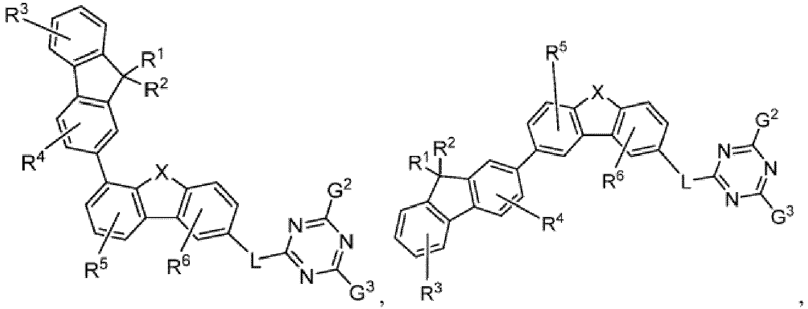


- Composé de la revendication 1, le composé ayant une structure de Formule II :

- Composé de la revendication 1, dans lequel G2 et G3 sont chacun indépendamment une fraction choisie dans le groupe constitué par :
 R1' et R2' étant indépendamment choisis dans le groupe constitué par hydrogène, deutérium, méthyle, éthyle, propyle, butyle, pentyle, hexyle, heptyle, octyle, isopropyle, isobutyle, terbutyle, terbutylméthyle, 2-éthylhexyle, 2-éthyloctyle, cyclopentyle, cyclohexyle, benzène, biphényle, terphényle et leurs combinaisons ;R1' et R2' étant facultativement attachés pour former un cycle ; etX' étant choisi dans un groupe constitué par O, S et Se.
 - Composé de la revendication 1, dans lequel L est une fraction choisie dans le groupe constitué par :


- Composé de la revendication 1, le composé étant choisi dans le groupe constitué par :


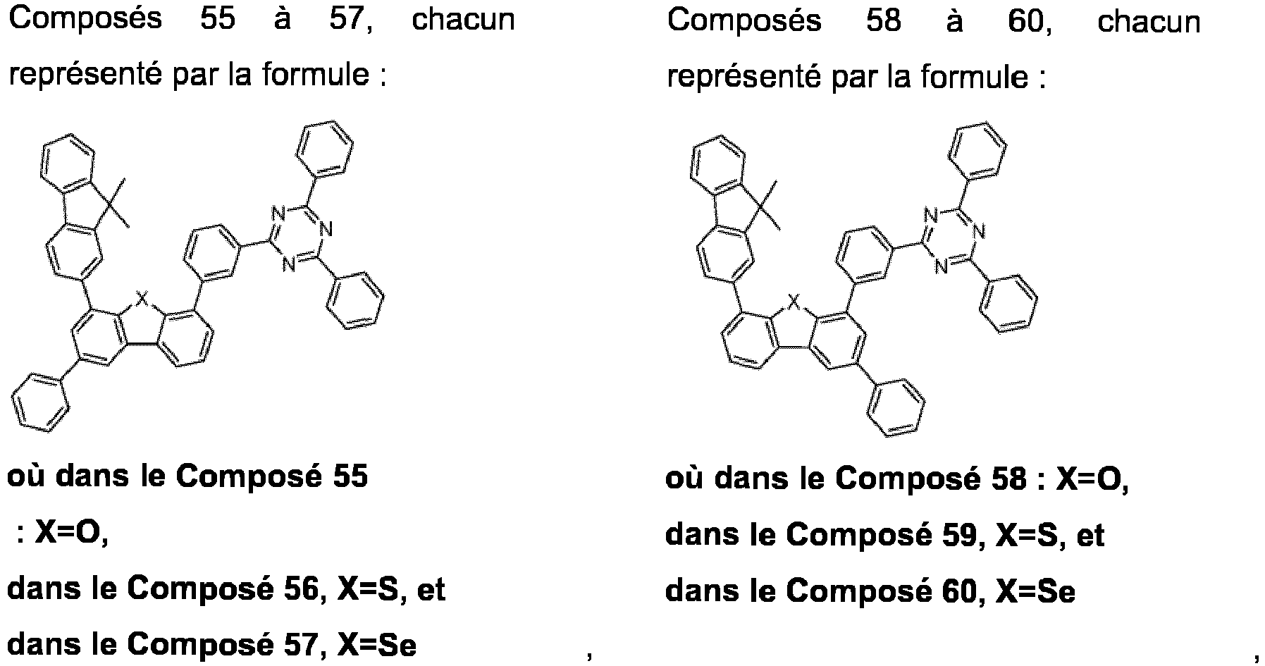


- Dispositif comprenant un ou plusieurs dispositifs électroluminescents organiques, au moins l'un du ou des dispositifs électroluminescents organiques comprenant :une anode ;une cathode ; etune couche organique, disposée entre l'anode et la cathode, comprenant un composé ayant la Formule I :
 X étant choisi dans un groupe constitué par O, S et Se ;G2 et G3 étant chacun indépendamment choisis dans le groupe constitué par benzène, biphényle, fluorène, naphtalène, phénanthrène, triphénylène, dibenzofurane, dibenzothiophène, dibenzosélénophène, pyridine, pyrimidine, quinoléine, isoquinoléine, phénanthroline, aza-fluorène et leurs combinaisons ;L étant choisi dans le groupe constitué par phényle, biphényle, terphényle et pyridine et leurs combinaisons ;G2, G3 et L étant chacun facultativement en outre substitués par un ou plusieurs substituants non fusionnés choisis dans le groupe constitué par deutérium, alkyle, alcoxyle, cycloalkyle, cycloalcoxyle, halogène, nitro, nitrile, silyle, benzène, biphényle, terphényle, pyridine et leurs combinaisons ;R3 représentant une mono, di, tri ou tétra substitution, ou aucune substitution ;R4, R5 et R6 représentant chacun indépendamment une mono, di ou tri substitution, ou aucune substitution ;R1, R2 et chaque R3, R4, R5 et R6 étant un substituant non fusionné choisi dans le groupe constitué par hydrogène, deutérium, alkyle, alcoxyle, cycloalkyle, cycloalcoxyle, halogène, nitro, nitrile, silyle, benzène, biphényle, terphényle, pyridine et leurs combinaisons ; etR1 et R2 étant facultativement attachés pour former un cycle.
 - Dispositif de la revendication 7, dans lequel le composé de la Formule I est choisi dans le groupe constitué par :


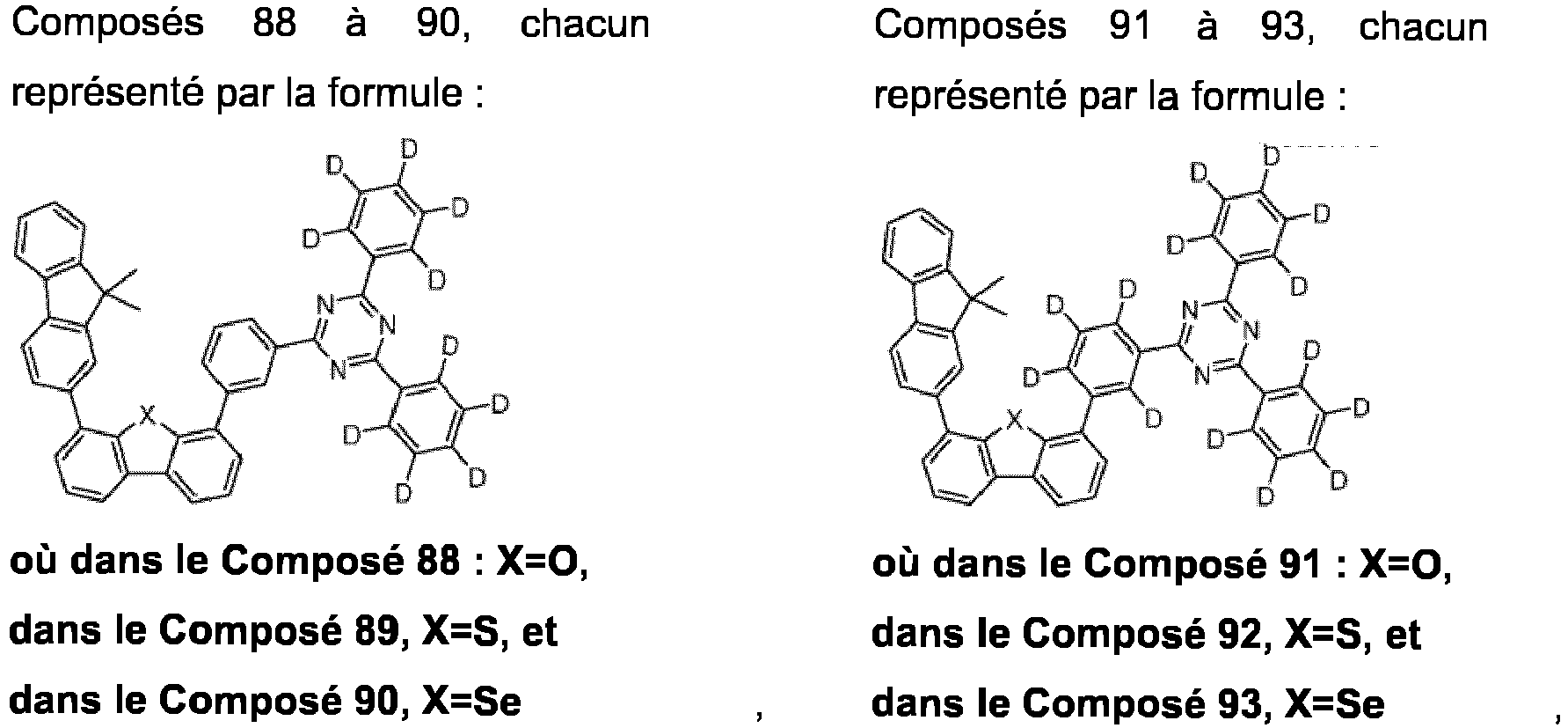

- Dispositif de la revendication 7, dans lequel la couche organique comprend en outre un dopant émissif, le dopant émissif étant un complexe de métal de transition ayant au moins un ligand choisi dans le groupe constitué par :


 Ra, Rb, Rc et Rd représentant une mono, di, tri ou tétra substitution, ou aucune substitution ;Ra, Rb, Rc et Rd étant indépendamment choisis dans le groupe constitué par hydrogène, deutérium, halogénure, alkyle, cycloalkyle, hétéroalkyle, arylalkyle, alcoxy, aryloxy, amino, silyle, alcényle, cycloalcényle, hétéroalcényle, alcynyle, aryle, hétéroaryle, acyle, carbonyle, acides carboxyliques, ester, nitrile, isonitrile, sulfanyle, sulfinyle, sulfonyle, phosphino et leurs combinaisons ; etdeux substituants adjacents de Ra, Rb, Rc et Rd étant facultativement attachés pour former un cycle fusionné ou former un ligand multidentate.
 - Dispositif de la revendication 7, dans lequel (A) la couche organique est une couche de blocage et le composé ayant la Formule I est une matière de blocage dans la couche organique, ou (B) la couche organique est une couche de transport d'électrons et le composé ayant la Formule I est une matière de transport d'électrons dans la couche organique.
- Composition de matières comprenant un premier composé et un second composé, le premier composé ayant une structure de Formule I :
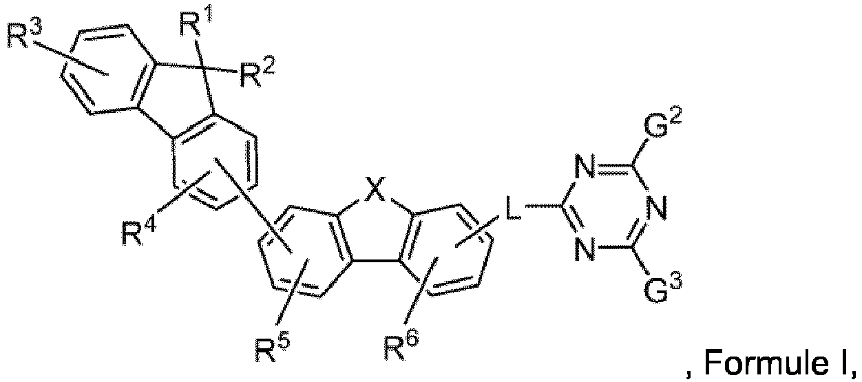 X étant choisi dans un groupe constitué par O, S et Se,G2 et G3 étant chacun indépendamment choisis dans le groupe constitué par benzène, biphényle, fluorène, naphtalène, phénanthrène, triphénylène, dibenzofurane, dibenzothiophène, dibenzosélénophène, pyridine, pyrimidine, quinoléine, isoquinoléine, phénanthroline, aza-fluorène et leurs combinaisons,L étant choisi dans le groupe constitué par phényle, biphényle, terphényle et pyridine et leurs combinaisons,G2, G3 et L étant chacun facultativement en outre substitués par un ou plusieurs substituants non fusionnés choisis dans le groupe constitué par deutérium, alkyle, alcoxyle, cycloalkyle, cycloalcoxyle, halogène, nitro, nitrile, silyle, benzène, biphényle, terphényle, pyridine et leurs combinaisons,R3 représentant une mono, di, tri ou tétra substitution, ou aucune substitution,R4, R5 et R6 représentant chacun indépendamment une mono, di ou tri substitution, ou aucune substitution,R1, R2 et chaque R3, R4, R5 et R6 étant un substituant non fusionné choisi dans le groupe constitué par hydrogène, deutérium, alkyle, alcoxyle, cycloalkyle, cycloalcoxyle, halogène, nitro, nitrile, silyle, benzène, biphényle, terphényle, pyridine et leurs combinaisons, etR1 et R2 étant facultativement attachés pour former un cycle ; etle second composé ayant une structure de Formule III :
 X étant choisi dans le groupe constitué par S, O, Se et NR',L2 étant choisi dans un groupe constitué par liaison directe, phényle, biphényle, terphényle, fluorène, triphénylène, dibenzofurane, dibenzothiophène, dibenzosélénophène, carbazole et pyridine et leurs combinaisons,L2 étant facultativement en outre substitué par un ou plusieurs substituants choisis dans un groupe constitué par hydrogène, deutérium, alkyle, alcoxyle, cycloalkyle, cycloalcoxyle, halogène, nitro, nitrile, silyle, aryle, hétéroaryle et leurs combinaisons,R', R7, R8, R9, R10 et R11 étant chacun un substituant non fusionné choisi dans le groupe constitué par hydrogène, deutérium, halogène, alkyle, cycloalkyle, hétéroalkyle, arylalkyle, alcoxy, aryloxy, amino, silyle, alcényle, cycloalcényle, hétéroalcényle, alcynyle, aryle, hétéroaryle, acyle, carbonyle, acide carboxylique, ester, nitrile, isonitrile, sulfanyle, sulfinyle, sulfonyle, phosphino et leurs combinaisons,R7, R8 et R11 représentant chacun indépendamment une mono, di, tri ou tétra substitution, ou aucune substitution, etR9 et R10 représentant chacun indépendamment une mono, di ou tri substitution, ou aucune substitution.
 - Composition de la revendication 11, dans laquelle le second composé est choisi dans le groupe constitué par :


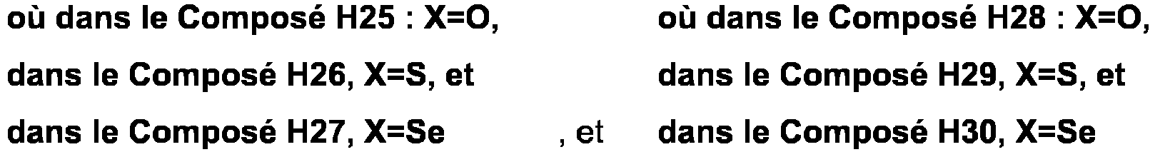
- Composition de la revendication 11, la composition étant choisie dans le groupe constitué par :
Compositions Premier composé Second composé CP1 Composé 2 Composé H2 CP2 Composé 2 Composé H5 CP3 Composé 2 Composé H8 CP4 Composé 2 Composé H17 CP5 Composé 2 Composé H26 CP6 Composé 5 Composé H11 CP7 Composé 5 Composé H14 CP8 Composé 5 Composé H29 CP9 Composé 65 Composé H2 CP10 Composé 65 Composé H5 - Dispositif comprenant un ou plusieurs dispositifs électroluminescents organiques, au moins l'un du ou des dispositifs électroluminescents organiques comprenant :une anode ;une cathode ; etune couche organique, disposée entre l'anode et la cathode, comprenant une première composition comprenant en outre un mélange d'un premier composé et d'un second composé ;le premier composé ayant une structure de Formule I :
 X étant choisi dans un groupe constitué par O, S et Se,G2 et G3 étant chacun indépendamment choisis dans le groupe constitué par benzène, biphényle, fluorène, naphtalène, phénanthrène, triphénylène, dibenzofurane, dibenzothiophène, dibenzosélénophène, pyridine, pyrimidine, quinoléine, isoquinoléine, phénanthroline, aza-fluorène et leurs combinaisons,L étant choisi dans le groupe constitué par phényle, biphényle, terphényle et pyridine et leurs combinaisons,G2, G3 et L étant chacun facultativement en outre substitués par un ou plusieurs substituants non fusionnés choisis dans le groupe constitué par deutérium, alkyle, alcoxyle, cycloalkyle, cycloalcoxyle, halogène, nitro, nitrile, silyle, benzène, biphényle, terphényle, pyridine et leurs combinaisons,R3 représentant une mono, di, tri ou tétra substitution, ou aucune substitution,R4, R5 et R6 représentant chacun indépendamment une mono, di ou tri substitution, ou aucune substitution,R1, R2 et chaque R3, R4, R5 et R6 étant un substituant non fusionné choisi dans le groupe constitué par hydrogène, deutérium, alkyle, alcoxyle, cycloalkyle, cycloalcoxyle, halogène, nitro, nitrile, silyle, benzène, biphényle, terphényle, pyridine et leurs combinaisons, etR1 et R2 étant facultativement attachés pour former un cycle ; etle second composé ayant une structure de Formule III :
 X étant choisi dans le groupe constitué par S, O, Se et NR',L2 étant choisi dans un groupe constitué par liaison directe, phényle, biphényle, terphényle, fluorène, triphénylène, dibenzofurane, dibenzothiophène, dibenzosélénophène, carbazole et pyridine et leurs combinaisons,L2 étant facultativement en outre substitué par un ou plusieurs substituants choisis dans un groupe constitué par hydrogène, deutérium, alkyle, alcoxyle, cycloalkyle, cycloalcoxyle, halogène, nitro, nitrile, silyle, aryle, hétéroaryle et leurs combinaisons,R', R7, R8, R9, R10 et R11 étant chacun un substituant non fusionné choisi dans le groupe constitué par hydrogène, deutérium, halogène, alkyle, cycloalkyle, hétéroalkyle, arylalkyle, alcoxy, aryloxy, amino, silyle, alcényle, cycloalcényle, hétéroalcényle, alcynyle, aryle, hétéroaryle, acyle, carbonyle, acide carboxylique, ester, nitrile, isonitrile, sulfanyle, sulfinyle, sulfonyle, phosphino et leurs combinaisons,R7, R8 et R11 représentant chacun indépendamment une mono, di, tri ou tétra substitution, ou aucune substitution, etR9 et R10 représentant chacun indépendamment une mono, di ou tri substitution, ou aucune substitution.
 - Procédé de fabrication d'un dispositif électroluminescent organique comprenant une première électrode, une seconde électrode et une première couche organique disposée entre la première électrode et la seconde électrode, la première couche organique comprenant une première composition comprenant un mélange d'un premier composé et d'un second composé, le procédé comprenant :se procurer un substrat ayant la première électrode disposée sur celui-ci ;déposer la première composition sur la première électrode ; etdéposer la seconde électrode sur la première couche organique, le premier composé ayant une structure de Formule I :
 X étant choisi dans un groupe constitué par O, S et Se,G2 et G3 étant chacun indépendamment choisis dans le groupe constitué par benzène, biphényle, fluorène, naphtalène, phénanthrène, triphénylène, dibenzofurane, dibenzothiophène, dibenzosélénophène, pyridine, pyrimidine, quinoléine, isoquinoléine, phénanthroline, aza-fluorène et leurs combinaisons,L étant choisi dans le groupe constitué par phényle, biphényle, terphényle et pyridine et leurs combinaisons,G2, G3 et L étant chacun facultativement en outre substitués par un ou plusieurs substituants non fusionnés choisis dans le groupe constitué par deutérium, alkyle, alcoxyle, cycloalkyle, cycloalcoxyle, halogène, nitro, nitrile, silyle, benzène, biphényle, terphényle, pyridine et leurs combinaisons,R3 représentant une mono, di, tri ou tétra substitution, ou aucune substitution,R4, R5 et R6 représentant chacun indépendamment une mono, di ou tri substitution, ou aucune substitution,R1, R2 et chaque R3, R4, R5 et R6 étant un substituant non fusionné choisi dans le groupe constitué par hydrogène, deutérium, alkyle, alcoxyle, cycloalkyle, cycloalcoxyle, halogène, nitro, nitrile, silyle, benzène, biphényle, terphényle, pyridine et leurs combinaisons, etR1 et R2 étant facultativement attachés pour former un cycle ; etle second composé ayant une structure de Formule III :
 X étant choisi dans le groupe constitué par S, O, Se et NR',L2 étant choisi dans un groupe constitué par liaison directe, phényle, biphényle, terphényle, fluorène, triphénylène, dibenzofurane, dibenzothiophène, dibenzosélénophène, carbazole et pyridine et leurs combinaisons,L2 étant facultativement en outre substitué par un ou plusieurs substituants choisis dans un groupe constitué par hydrogène, deutérium, alkyle, alcoxyle, cycloalkyle, cycloalcoxyle, halogène, nitro, nitrile, silyle, aryle, hétéroaryle et leurs combinaisons,R', R7, R8, R9, R10 et R11 étant chacun un substituant non fusionné choisi dans le groupe constitué par hydrogène, deutérium, halogène, alkyle, cycloalkyle, hétéroalkyle, arylalkyle, alcoxy, aryloxy, amino, silyle, alcényle, cycloalcényle, hétéroalcényle, alcynyle, aryle, hétéroaryle, acyle, carbonyle, acide carboxylique, ester, nitrile, isonitrile, sulfanyle, sulfinyle, sulfonyle, phosphino et leurs combinaisons,R7, R8 et R11 représentant chacun indépendamment une mono, di, tri ou tétra substitution, ou aucune substitution, etR9 et R10 représentant chacun indépendamment une mono, di ou tri substitution, ou aucune substitution.
Applications Claiming Priority (1)
| Application Number | Priority Date | Filing Date | Title |
|---|---|---|---|
| US14/591,555 US9406892B2 (en) | 2015-01-07 | 2015-01-07 | Organic electroluminescent materials and devices |
Publications (2)
| Publication Number | Publication Date |
|---|---|
| EP3043398A1 EP3043398A1 (fr) | 2016-07-13 |
| EP3043398B1 true EP3043398B1 (fr) | 2018-04-04 |
Family
ID=55068826
Family Applications (1)
| Application Number | Title | Priority Date | Filing Date |
|---|---|---|---|
| EP15202033.5A Active EP3043398B1 (fr) | 2015-01-07 | 2015-12-22 | Matériaux et dispositifs électroluminescents organiques |
Country Status (5)
| Country | Link |
|---|---|
| US (1) | US9406892B2 (fr) |
| EP (1) | EP3043398B1 (fr) |
| JP (1) | JP6612623B2 (fr) |
| KR (1) | KR102484830B1 (fr) |
| CN (1) | CN105753847B (fr) |
Families Citing this family (59)
| Publication number | Priority date | Publication date | Assignee | Title |
|---|---|---|---|---|
| US20130203996A1 (en) | 2010-04-30 | 2013-08-08 | Jian Li | Synthesis of Four Coordinated Palladium Complexes and Their Applications in Light Emitting Devices Thereof |
| WO2012162488A1 (fr) | 2011-05-26 | 2012-11-29 | Arizona Board Of Regents Acting For And On Behalf Of Arizona State University | Synthèse de complexes de platine et de palladium comme émetteurs phosphorescents à bande étroite pour dispositifs d'affichage pleine couleur |
| US9882150B2 (en) | 2012-09-24 | 2018-01-30 | Arizona Board Of Regents For And On Behalf Of Arizona State University | Metal compounds, methods, and uses thereof |
| JP6804823B2 (ja) | 2013-10-14 | 2020-12-23 | アリゾナ・ボード・オブ・リージェンツ・オン・ビハーフ・オブ・アリゾナ・ステイト・ユニバーシティーArizona Board of Regents on behalf of Arizona State University | 白金錯体およびデバイス |
| US10020455B2 (en) | 2014-01-07 | 2018-07-10 | Arizona Board Of Regents On Behalf Of Arizona State University | Tetradentate platinum and palladium complex emitters containing phenyl-pyrazole and its analogues |
| US9941479B2 (en) | 2014-06-02 | 2018-04-10 | Arizona Board Of Regents On Behalf Of Arizona State University | Tetradentate cyclometalated platinum complexes containing 9,10-dihydroacridine and its analogues |
| US9923155B2 (en) | 2014-07-24 | 2018-03-20 | Arizona Board Of Regents On Behalf Of Arizona State University | Tetradentate platinum (II) complexes cyclometalated with functionalized phenyl carbene ligands and their analogues |
| US10793546B2 (en) | 2014-08-15 | 2020-10-06 | Arizona Board Of Regents On Behalf Of Arizona State University | Non-platinum metal complexes for excimer based single dopant white organic light emitting diodes |
| US11329244B2 (en) | 2014-08-22 | 2022-05-10 | Arizona Board Of Regents On Behalf Of Arizona State University | Organic light-emitting diodes with fluorescent and phosphorescent emitters |
| US9865825B2 (en) | 2014-11-10 | 2018-01-09 | Arizona Board Of Regents On Behalf Of Arizona State University | Emitters based on octahedral metal complexes |
| US10033003B2 (en) | 2014-11-10 | 2018-07-24 | Arizona Board Of Regents On Behalf Of Arizona State University | Tetradentate metal complexes with carbon group bridging ligands |
| US9879039B2 (en) | 2015-06-03 | 2018-01-30 | Arizona Board Of Regents On Behalf Of Arizona State University | Tetradentate and octahedral metal complexes containing naphthyridinocarbazole and its analogues |
| US10158091B2 (en) | 2015-08-04 | 2018-12-18 | Arizona Board Of Regents On Behalf Of Arizona State University | Tetradentate platinum (II) and palladium (II) complexes, devices, and uses thereof |
| KR101919194B1 (ko) * | 2015-09-15 | 2018-11-15 | 주식회사 엘지화학 | 헤테로고리 화합물 및 이를 포함하는 유기 발광 소자 |
| US11335865B2 (en) | 2016-04-15 | 2022-05-17 | Arizona Board Of Regents On Behalf Of Arizona State University | OLED with multi-emissive material layer |
| KR101849747B1 (ko) | 2016-07-20 | 2018-05-31 | 주식회사 엘지화학 | 신규한 헤테로 고리 화합물 및 이를 이용한 유기발광 소자 |
| WO2018034340A1 (fr) * | 2016-08-19 | 2018-02-22 | 株式会社Kyulux | Matériau de transport de charge, composé, matériau de fluorescence retardée, et élément luminescent organique |
| US10177323B2 (en) | 2016-08-22 | 2019-01-08 | Arizona Board Of Regents On Behalf Of Arizona State University | Tetradentate platinum (II) and palladium (II) complexes and octahedral iridium complexes employing azepine functional groups and their analogues |
| KR20210083134A (ko) | 2016-10-12 | 2021-07-06 | 아리조나 보드 오브 리젠츠 온 비하프 오브 아리조나 스테이트 유니버시티 | 협대역 적색 인광성 4좌 백금(ii) 착물 |
| KR101885899B1 (ko) * | 2016-11-07 | 2018-08-06 | 주식회사 엘지화학 | 신규한 헤테로 고리 화합물 및 이를 이용한 유기발광 소자 |
| WO2018084423A2 (fr) * | 2016-11-07 | 2018-05-11 | 주식회사 엘지화학 | Nouveau composé hétérocyclique et élément électroluminescent organique l'utilisant |
| US10897016B2 (en) | 2016-11-14 | 2021-01-19 | Universal Display Corporation | Organic electroluminescent materials and devices |
| US11183670B2 (en) | 2016-12-16 | 2021-11-23 | Arizona Board Of Regents On Behalf Of Arizona State University | Organic light emitting diode with split emissive layer |
| KR20190139835A (ko) | 2017-01-27 | 2019-12-18 | 아리조나 보드 오브 리젠츠 온 비하프 오브 아리조나 스테이트 유니버시티 | 피리도-피롤로-아크리딘 및 유사체를 사용하는 금속 보조 지연 형광 이미터 |
| KR20180108426A (ko) | 2017-03-24 | 2018-10-04 | 희성소재 (주) | 헤테로고리 화합물 및 이를 포함하는 유기 발광 소자 |
| KR20180108425A (ko) | 2017-03-24 | 2018-10-04 | 희성소재 (주) | 헤테로고리 화합물 및 이를 포함하는 유기 발광 소자 |
| JP2018163975A (ja) * | 2017-03-24 | 2018-10-18 | 出光興産株式会社 | 組成物、有機エレクトロルミネッセンス素子用材料、組成物膜、有機エレクトロルミネッセンス素子、及び電子機器 |
| US10516117B2 (en) | 2017-05-19 | 2019-12-24 | Arizona Board Of Regents On Behalf Of Arizona State University | Metal-assisted delayed fluorescent emttters employing benzo-imidazo-phenanthridine and analogues |
| US11101435B2 (en) | 2017-05-19 | 2021-08-24 | Arizona Board Of Regents On Behalf Of Arizona State University | Tetradentate platinum and palladium complexes based on biscarbazole and analogues |
| KR102232510B1 (ko) * | 2017-05-26 | 2021-03-26 | 삼성에스디아이 주식회사 | 인광 호스트용 조성물, 유기 광전자 소자 및 표시 장치 |
| CN110520419B (zh) | 2017-07-19 | 2023-05-26 | 株式会社Lg化学 | 新的杂环化合物和包含其的有机发光器件 |
| KR101856728B1 (ko) | 2017-08-10 | 2018-05-10 | 주식회사 엘지화학 | 유기 발광 소자 |
| KR102038031B1 (ko) | 2017-09-15 | 2019-10-30 | 엘티소재주식회사 | 헤테로고리 화합물 및 이를 포함하는 유기 발광 소자 |
| WO2019066242A1 (fr) * | 2017-09-29 | 2019-04-04 | 덕산네오룩스 주식회사 | Composé destiné à un élément électronique organique, élément électronique organique l'utilisant, et dispositif électronique le comprenant |
| KR102418440B1 (ko) | 2017-09-29 | 2022-07-07 | 덕산네오룩스 주식회사 | 유기전기 소자용 화합물, 이를 이용한 유기전기소자 및 그 전자 장치 |
| WO2019079508A2 (fr) | 2017-10-17 | 2019-04-25 | Jian Li | Excimères phosphorescents à orientation moléculaire préférée en tant qu'émetteurs monochromatiques destinés à des applications d'affichage et d'éclairage |
| WO2019079505A1 (fr) | 2017-10-17 | 2019-04-25 | Jian Li | Matériaux de blocage de trous pour diodes électroluminescentes organiques |
| CN109928961B (zh) * | 2017-12-15 | 2021-06-15 | 广东阿格蕾雅光电材料有限公司 | 含有4-硫砜芳基二苯并呋喃的光电材料及应用 |
| US11706977B2 (en) | 2018-01-11 | 2023-07-18 | Samsung Electronics Co., Ltd. | Heterocyclic compound, composition including the same, and organic light-emitting device including the heterocyclic compound |
| WO2019163826A1 (fr) * | 2018-02-20 | 2019-08-29 | 出光興産株式会社 | Nouveau composé et élément électroluminescent organique l'utilisant |
| US11370782B2 (en) | 2018-03-06 | 2022-06-28 | Lg Chem, Ltd. | Compound and organic light emitting device comprising the same |
| WO2019209031A1 (fr) * | 2018-04-24 | 2019-10-31 | 주식회사 엘지화학 | Nouveau composé hétérocyclique et dispositif électroluminescent organique l'utilisant |
| KR102206482B1 (ko) | 2018-04-24 | 2021-01-22 | 주식회사 엘지화학 | 신규한 헤테로 고리 화합물 및 이를 이용한 유기발광 소자 |
| KR102044943B1 (ko) | 2018-05-28 | 2019-11-14 | 삼성에스디아이 주식회사 | 화합물, 조성물, 유기 광전자 소자 및 표시 장치 |
| CN111683940B (zh) * | 2018-05-29 | 2023-09-12 | 株式会社Lg化学 | 杂环化合物及包含其的有机发光器件 |
| KR20210016423A (ko) | 2018-05-30 | 2021-02-15 | 메르크 파텐트 게엠베하 | 유기 전자 디바이스용 조성물 |
| CN111683941B (zh) * | 2018-06-14 | 2023-09-12 | 株式会社Lg化学 | 杂环化合物和包含其的有机发光器件 |
| US11802124B2 (en) | 2018-07-09 | 2023-10-31 | Lg Chem, Ltd. | Compound and organic light emitting diode comprising same |
| KR102599592B1 (ko) * | 2018-08-30 | 2023-11-07 | 솔루스첨단소재 주식회사 | 유기 화합물 및 이를 이용한 유기 전계 발광 소자 |
| KR102321311B1 (ko) * | 2018-11-06 | 2021-11-03 | 주식회사 엘지화학 | 신규한 화합물 및 이를 이용한 유기 발광 소자 |
| WO2020096350A1 (fr) * | 2018-11-06 | 2020-05-14 | 주식회사 엘지화학 | Nouveau composé et élément électroluminescent organique l'utilisant |
| KR20200061721A (ko) * | 2018-11-26 | 2020-06-03 | 두산솔루스 주식회사 | 유기 화합물 및 이를 이용한 유기 전계 발광 소자 |
| US11878988B2 (en) | 2019-01-24 | 2024-01-23 | Arizona Board Of Regents On Behalf Of Arizona State University | Blue phosphorescent emitters employing functionalized imidazophenthridine and analogues |
| US11594691B2 (en) | 2019-01-25 | 2023-02-28 | Arizona Board Of Regents On Behalf Of Arizona State University | Light outcoupling efficiency of phosphorescent OLEDs by mixing horizontally aligned fluorescent emitters |
| CN110373182B (zh) * | 2019-07-10 | 2023-06-06 | 吉林奥来德光电材料股份有限公司 | 一种有机发光化合物及其制备方法和器件 |
| US11785838B2 (en) | 2019-10-02 | 2023-10-10 | Arizona Board Of Regents On Behalf Of Arizona State University | Green and red organic light-emitting diodes employing excimer emitters |
| KR102537419B1 (ko) * | 2019-11-04 | 2023-05-25 | 주식회사 엘지화학 | 신규한 화합물 및 이를 이용한 유기 발광 소자 |
| US11945985B2 (en) | 2020-05-19 | 2024-04-02 | Arizona Board Of Regents On Behalf Of Arizona State University | Metal assisted delayed fluorescent emitters for organic light-emitting diodes |
| WO2023063163A1 (fr) * | 2021-10-14 | 2023-04-20 | 出光興産株式会社 | Poudre mélangée pour élément électroluminescent organique, son procédé de production, procédé de fabrication d'élément électroluminescent organique au moyen de ladite poudre mélangée, procédé de sélection de composé dans ladite poudre mélangée, et composition pour dépôt sous vide |
Family Cites Families (147)
| Publication number | Priority date | Publication date | Assignee | Title |
|---|---|---|---|---|
| US4769292A (en) | 1987-03-02 | 1988-09-06 | Eastman Kodak Company | Electroluminescent device with modified thin film luminescent zone |
| GB8909011D0 (en) | 1989-04-20 | 1989-06-07 | Friend Richard H | Electroluminescent devices |
| US5061569A (en) | 1990-07-26 | 1991-10-29 | Eastman Kodak Company | Electroluminescent device with organic electroluminescent medium |
| DE69412567T2 (de) | 1993-11-01 | 1999-02-04 | Hodogaya Chemical Co Ltd | Aminverbindung und sie enthaltende Elektrolumineszenzvorrichtung |
| US5703436A (en) | 1994-12-13 | 1997-12-30 | The Trustees Of Princeton University | Transparent contacts for organic devices |
| US5707745A (en) | 1994-12-13 | 1998-01-13 | The Trustees Of Princeton University | Multicolor organic light emitting devices |
| US5844363A (en) | 1997-01-23 | 1998-12-01 | The Trustees Of Princeton Univ. | Vacuum deposited, non-polymeric flexible organic light emitting devices |
| US5834893A (en) | 1996-12-23 | 1998-11-10 | The Trustees Of Princeton University | High efficiency organic light emitting devices with light directing structures |
| US6013982A (en) | 1996-12-23 | 2000-01-11 | The Trustees Of Princeton University | Multicolor display devices |
| US6091195A (en) | 1997-02-03 | 2000-07-18 | The Trustees Of Princeton University | Displays having mesa pixel configuration |
| US6303238B1 (en) | 1997-12-01 | 2001-10-16 | The Trustees Of Princeton University | OLEDs doped with phosphorescent compounds |
| US6337102B1 (en) | 1997-11-17 | 2002-01-08 | The Trustees Of Princeton University | Low pressure vapor phase deposition of organic thin films |
| US6087196A (en) | 1998-01-30 | 2000-07-11 | The Trustees Of Princeton University | Fabrication of organic semiconductor devices using ink jet printing |
| US6528187B1 (en) | 1998-09-08 | 2003-03-04 | Fuji Photo Film Co., Ltd. | Material for luminescence element and luminescence element using the same |
| US6830828B2 (en) | 1998-09-14 | 2004-12-14 | The Trustees Of Princeton University | Organometallic complexes as phosphorescent emitters in organic LEDs |
| US6097147A (en) | 1998-09-14 | 2000-08-01 | The Trustees Of Princeton University | Structure for high efficiency electroluminescent device |
| KR100744199B1 (ko) * | 1999-05-13 | 2007-08-01 | 더 트러스티즈 오브 프린스턴 유니버시티 | 전계인광에 기초한 고 효율의 유기 발광장치 |
| US6294398B1 (en) | 1999-11-23 | 2001-09-25 | The Trustees Of Princeton University | Method for patterning devices |
| US6458475B1 (en) | 1999-11-24 | 2002-10-01 | The Trustee Of Princeton University | Organic light emitting diode having a blue phosphorescent molecule as an emitter |
| KR100377321B1 (ko) | 1999-12-31 | 2003-03-26 | 주식회사 엘지화학 | 피-형 반도체 성질을 갖는 유기 화합물을 포함하는 전기소자 |
| US6821643B1 (en) | 2000-01-21 | 2004-11-23 | Xerox Corporation | Electroluminescent (EL) devices |
| US20020121638A1 (en) | 2000-06-30 | 2002-09-05 | Vladimir Grushin | Electroluminescent iridium compounds with fluorinated phenylpyridines, phenylpyrimidines, and phenylquinolines and devices made with such compounds |
| CN100505375C (zh) | 2000-08-11 | 2009-06-24 | 普林斯顿大学理事会 | 有机金属化合物和发射转换有机电致磷光 |
| US6579630B2 (en) | 2000-12-07 | 2003-06-17 | Canon Kabushiki Kaisha | Deuterated semiconducting organic compounds used for opto-electronic devices |
| JP3812730B2 (ja) | 2001-02-01 | 2006-08-23 | 富士写真フイルム株式会社 | 遷移金属錯体及び発光素子 |
| JP4307000B2 (ja) | 2001-03-08 | 2009-08-05 | キヤノン株式会社 | 金属配位化合物、電界発光素子及び表示装置 |
| JP4310077B2 (ja) | 2001-06-19 | 2009-08-05 | キヤノン株式会社 | 金属配位化合物及び有機発光素子 |
| ATE431970T1 (de) | 2001-06-20 | 2009-06-15 | Showa Denko Kk | Licht emittierendes material und organische leuchtdiode |
| US7071615B2 (en) | 2001-08-20 | 2006-07-04 | Universal Display Corporation | Transparent electrodes |
| US7250226B2 (en) | 2001-08-31 | 2007-07-31 | Nippon Hoso Kyokai | Phosphorescent compound, a phosphorescent composition and an organic light-emitting device |
| US7431968B1 (en) | 2001-09-04 | 2008-10-07 | The Trustees Of Princeton University | Process and apparatus for organic vapor jet deposition |
| US6835469B2 (en) | 2001-10-17 | 2004-12-28 | The University Of Southern California | Phosphorescent compounds and devices comprising the same |
| US7166368B2 (en) | 2001-11-07 | 2007-01-23 | E. I. Du Pont De Nemours And Company | Electroluminescent platinum compounds and devices made with such compounds |
| US6863997B2 (en) | 2001-12-28 | 2005-03-08 | The Trustees Of Princeton University | White light emitting OLEDs from combined monomer and aggregate emission |
| KR100691543B1 (ko) | 2002-01-18 | 2007-03-09 | 주식회사 엘지화학 | 새로운 전자 수송용 물질 및 이를 이용한 유기 발광 소자 |
| US6878975B2 (en) | 2002-02-08 | 2005-04-12 | Agilent Technologies, Inc. | Polarization field enhanced tunnel structures |
| US7132174B2 (en) * | 2002-05-31 | 2006-11-07 | E. I. Du Pont De Nemours And Company | Copolymers having tunable energy levels and color of emission |
| US20030230980A1 (en) | 2002-06-18 | 2003-12-18 | Forrest Stephen R | Very low voltage, high efficiency phosphorescent oled in a p-i-n structure |
| US7189989B2 (en) | 2002-08-22 | 2007-03-13 | Fuji Photo Film Co., Ltd. | Light emitting element |
| WO2004020549A1 (fr) | 2002-08-27 | 2004-03-11 | Fujitsu Limited | Complexes organometalliques, dispositifs organiques electroluminescents et ecrans organiques electroluminescents |
| US6687266B1 (en) | 2002-11-08 | 2004-02-03 | Universal Display Corporation | Organic light emitting materials and devices |
| JP4365199B2 (ja) | 2002-12-27 | 2009-11-18 | 富士フイルム株式会社 | 有機電界発光素子 |
| JP4365196B2 (ja) | 2002-12-27 | 2009-11-18 | 富士フイルム株式会社 | 有機電界発光素子 |
| EP2062908B1 (fr) | 2003-03-24 | 2016-07-13 | University of Southern California | Complexes des métaux de transition contenant pyrazolylcarbazoles comme ligands |
| US7090928B2 (en) | 2003-04-01 | 2006-08-15 | The University Of Southern California | Binuclear compounds |
| WO2004093207A2 (fr) | 2003-04-15 | 2004-10-28 | Covion Organic Semiconductors Gmbh | Melanges de semi-conducteurs organiques aptes a l'emission et de matieres matricielles, leur utilisation et composants electroniques contenant ces melanges |
| US7029765B2 (en) | 2003-04-22 | 2006-04-18 | Universal Display Corporation | Organic light emitting devices having reduced pixel shrinkage |
| WO2004107822A1 (fr) | 2003-05-29 | 2004-12-09 | Nippon Steel Chemical Co., Ltd. | Element electroluminescent organique |
| JP2005011610A (ja) | 2003-06-18 | 2005-01-13 | Nippon Steel Chem Co Ltd | 有機電界発光素子 |
| US20050025993A1 (en) | 2003-07-25 | 2005-02-03 | Thompson Mark E. | Materials and structures for enhancing the performance of organic light emitting devices |
| TWI390006B (zh) | 2003-08-07 | 2013-03-21 | Nippon Steel Chemical Co | Organic EL materials with aluminum clamps |
| DE10338550A1 (de) | 2003-08-19 | 2005-03-31 | Basf Ag | Übergangsmetallkomplexe mit Carbenliganden als Emitter für organische Licht-emittierende Dioden (OLEDs) |
| US20060269780A1 (en) | 2003-09-25 | 2006-11-30 | Takayuki Fukumatsu | Organic electroluminescent device |
| JP4822687B2 (ja) | 2003-11-21 | 2011-11-24 | 富士フイルム株式会社 | 有機電界発光素子 |
| US7332232B2 (en) | 2004-02-03 | 2008-02-19 | Universal Display Corporation | OLEDs utilizing multidentate ligand systems |
| EP1725079B1 (fr) | 2004-03-11 | 2013-05-08 | Mitsubishi Chemical Corporation | Composition pour une couche transportant des charges et pour un composé ionique, couche transportant des charges et dispositif électroluminescent organique utilisant celle-ci, procédé de fabrication d'un dispositif électroluminescent organique et procédé de fabrication |
| TW200531592A (en) | 2004-03-15 | 2005-09-16 | Nippon Steel Chemical Co | Organic electroluminescent device |
| JP4869565B2 (ja) | 2004-04-23 | 2012-02-08 | 富士フイルム株式会社 | 有機電界発光素子 |
| US7393599B2 (en) | 2004-05-18 | 2008-07-01 | The University Of Southern California | Luminescent compounds with carbene ligands |
| US7445855B2 (en) | 2004-05-18 | 2008-11-04 | The University Of Southern California | Cationic metal-carbene complexes |
| US7534505B2 (en) | 2004-05-18 | 2009-05-19 | The University Of Southern California | Organometallic compounds for use in electroluminescent devices |
| US7154114B2 (en) | 2004-05-18 | 2006-12-26 | Universal Display Corporation | Cyclometallated iridium carbene complexes for use as hosts |
| US7491823B2 (en) | 2004-05-18 | 2009-02-17 | The University Of Southern California | Luminescent compounds with carbene ligands |
| US7279704B2 (en) | 2004-05-18 | 2007-10-09 | The University Of Southern California | Complexes with tridentate ligands |
| WO2005123873A1 (fr) | 2004-06-17 | 2005-12-29 | Konica Minolta Holdings, Inc. | Mat)riau de dispositif )lectroluminescent organique, dispositif )lectroluminescent organique, )cran et dispositif d')clairage |
| KR101272490B1 (ko) | 2004-06-28 | 2013-06-07 | 시바 홀딩 인크 | 트리아졸 및 벤조트리아졸을 갖는 전계발광 금속 착물 |
| US20060008670A1 (en) | 2004-07-06 | 2006-01-12 | Chun Lin | Organic light emitting materials and devices |
| EP2271183B1 (fr) | 2004-07-23 | 2015-03-18 | Konica Minolta Holdings, Inc. | Dispositif et affichage electroluminescents organiques et dispositif d´eclairage |
| DE102004057072A1 (de) | 2004-11-25 | 2006-06-01 | Basf Ag | Verwendung von Übergangsmetall-Carbenkomplexen in organischen Licht-emittierenden Dioden (OLEDs) |
| WO2006072002A2 (fr) | 2004-12-30 | 2006-07-06 | E.I. Dupont De Nemours And Company | Complexes organometalliques |
| JPWO2006082742A1 (ja) | 2005-02-04 | 2008-06-26 | コニカミノルタホールディングス株式会社 | 有機エレクトロルミネッセンス素子材料、有機エレクトロルミネッセンス素子、表示装置及び照明装置 |
| KR100803125B1 (ko) | 2005-03-08 | 2008-02-14 | 엘지전자 주식회사 | 적색 인광 화합물 및 이를 사용한 유기전계발광소자 |
| WO2006098120A1 (fr) | 2005-03-16 | 2006-09-21 | Konica Minolta Holdings, Inc. | Materiau pour dispositif electroluminescent organique et dispositif electroluminescent organique |
| DE102005014284A1 (de) | 2005-03-24 | 2006-09-28 | Basf Ag | Verwendung von Verbindungen, welche aromatische oder heteroaromatische über Carbonyl-Gruppen enthaltende Gruppen verbundene Ringe enthalten, als Matrixmaterialien in organischen Leuchtdioden |
| WO2006103874A1 (fr) | 2005-03-29 | 2006-10-05 | Konica Minolta Holdings, Inc. | Materiau de dispositif electroluminescent organique, dispositif electroluminescent organique, ecran et dispositif d’eclairage |
| WO2006114966A1 (fr) | 2005-04-18 | 2006-11-02 | Konica Minolta Holdings, Inc. | Dispositif électroluminescent organique, affichage et dispositif d'illumination |
| US7807275B2 (en) | 2005-04-21 | 2010-10-05 | Universal Display Corporation | Non-blocked phosphorescent OLEDs |
| JP4533796B2 (ja) | 2005-05-06 | 2010-09-01 | 富士フイルム株式会社 | 有機電界発光素子 |
| US9051344B2 (en) | 2005-05-06 | 2015-06-09 | Universal Display Corporation | Stability OLED materials and devices |
| CN103746080B (zh) | 2005-05-31 | 2019-03-08 | 通用显示公司 | 发射磷光的二极管中的苯并[9,10]菲基质 |
| JP4976288B2 (ja) | 2005-06-07 | 2012-07-18 | 新日鐵化学株式会社 | 有機金属錯体及びこれを用いた有機電界発光素子 |
| KR101294905B1 (ko) | 2005-06-27 | 2013-08-09 | 이 아이 듀폰 디 네모아 앤드 캄파니 | 전기 전도성 중합체 조성물 |
| US20090039771A1 (en) | 2005-07-01 | 2009-02-12 | Konica Minolta Holdings, Inc. | Organic electroluminescent element material, organic electroluminescent element, display device and lighting device |
| WO2007028417A1 (fr) | 2005-09-07 | 2007-03-15 | Technische Universität Braunschweig | Émetteur triple comportant des anneaux à cinq éléments condensés |
| JP4887731B2 (ja) | 2005-10-26 | 2012-02-29 | コニカミノルタホールディングス株式会社 | 有機エレクトロルミネッセンス素子、表示装置及び照明装置 |
| CN101321755B (zh) | 2005-12-01 | 2012-04-18 | 新日铁化学株式会社 | 有机电致发光元件用化合物及有机电致发光元件 |
| JPWO2007063796A1 (ja) | 2005-12-01 | 2009-05-07 | 新日鐵化学株式会社 | 有機電界発光素子 |
| CN101415718B (zh) | 2006-02-10 | 2013-05-29 | 通用显示公司 | 环金属化的咪唑并[1,2-f]菲啶和二咪唑并[1,2-a:1',2'-c]喹唑啉配位体和其等电子和苯并环化类似物的金属络合物 |
| JP4823730B2 (ja) | 2006-03-20 | 2011-11-24 | 新日鐵化学株式会社 | 発光層化合物及び有機電界発光素子 |
| WO2007125714A1 (fr) | 2006-04-26 | 2007-11-08 | Idemitsu Kosan Co., Ltd. | Dérivé d'amine aromatique, élément électroluminescent organique employant ledit dérivé |
| KR101384046B1 (ko) | 2006-05-11 | 2014-04-09 | 이데미쓰 고산 가부시키가이샤 | 유기 전계발광 소자 |
| KR20090016684A (ko) | 2006-06-02 | 2009-02-17 | 이데미쓰 고산 가부시키가이샤 | 유기 전기발광 소자용 재료 및 그것을 이용한 유기 전기발광 소자 |
| KR20090040896A (ko) | 2006-08-23 | 2009-04-27 | 이데미쓰 고산 가부시키가이샤 | 방향족 아민 유도체 및 이들을 이용한 유기 전기발광 소자 |
| JP5589251B2 (ja) | 2006-09-21 | 2014-09-17 | コニカミノルタ株式会社 | 有機エレクトロルミネッセンス素子材料 |
| CN101511834B (zh) | 2006-11-09 | 2013-03-27 | 新日铁化学株式会社 | 有机场致发光元件用化合物及有机场致发光元件 |
| JP5133259B2 (ja) | 2006-11-24 | 2013-01-30 | 出光興産株式会社 | 芳香族アミン誘導体及びそれを用いた有機エレクトロルミネッセンス素子 |
| US8778508B2 (en) | 2006-12-08 | 2014-07-15 | Universal Display Corporation | Light-emitting organometallic complexes |
| US8119255B2 (en) | 2006-12-08 | 2012-02-21 | Universal Display Corporation | Cross-linkable iridium complexes and organic light-emitting devices using the same |
| EP2112994B1 (fr) | 2007-02-23 | 2011-01-26 | Basf Se | Complexes métalliques électroluminescents contenant des benzotriazoles |
| DE502008002309D1 (de) | 2007-04-26 | 2011-02-24 | Basf Se | Silane enthaltend phenothiazin-s-oxid oder phenothiazin-s,s-dioxid-gruppen und deren verwendung in oleds |
| WO2008156879A1 (fr) | 2007-06-20 | 2008-12-24 | Universal Display Corporation | Matériaux à base d'imidazophénantridine phosphorescente bleue |
| KR101539789B1 (ko) | 2007-06-22 | 2015-07-27 | 바스프 에스이 | 발광 cu(i) 착물 |
| US20090001477A1 (en) | 2007-06-29 | 2009-01-01 | Louis Lu-Chen Hsu | Hybrid Fully-Silicided (FUSI)/Partially-Silicided (PASI) Structures |
| US8029697B2 (en) | 2007-07-07 | 2011-10-04 | Idemitsu Kosan Co., Ltd. | Naphthalene derivative, material for organic electroluminescence device, and organic electroluminescence device using the same |
| US8779655B2 (en) | 2007-07-07 | 2014-07-15 | Idemitsu Kosan Co., Ltd. | Organic electroluminescence device and material for organic electroluminescence device |
| WO2009008205A1 (fr) | 2007-07-07 | 2009-01-15 | Idemitsu Kosan Co., Ltd. | Dispositif électroluminescent organique et matériau pour un dispositif électroluminescent organique |
| US20090045731A1 (en) | 2007-07-07 | 2009-02-19 | Idemitsu Kosan Co., Ltd. | Organic electroluminescence device and material for organic electroluminescence device |
| US8221907B2 (en) | 2007-07-07 | 2012-07-17 | Idemitsu Kosan Co., Ltd. | Chrysene derivative and organic electroluminescent device using the same |
| US7968213B2 (en) | 2007-07-10 | 2011-06-28 | Idemitsu Kosan Co., Ltd. | Material for organic electroluminescence device and organic electroluminescence device utilizing the same |
| US8080658B2 (en) | 2007-07-10 | 2011-12-20 | Idemitsu Kosan Co., Ltd. | Material for organic electroluminescent element and organic electroluminescent element employing the same |
| CN101688052A (zh) | 2007-07-27 | 2010-03-31 | E.I.内穆尔杜邦公司 | 包含无机纳米颗粒的导电聚合物的含水分散体 |
| KR101787850B1 (ko) * | 2007-08-08 | 2017-10-18 | 유니버셜 디스플레이 코포레이션 | 트리페닐렌기를 포함하는 벤조 융합 티오펜 또는 벤조 융합 푸란 화합물 |
| JP2009040728A (ja) | 2007-08-09 | 2009-02-26 | Canon Inc | 有機金属錯体及びこれを用いた有機発光素子 |
| EP2203461B1 (fr) | 2007-10-17 | 2011-08-10 | Basf Se | Complexes de métaux de transition avec des ligands carbène pontés, et leur utilisation dans des diodes électroluminescentes organiques (oled) |
| US20090101870A1 (en) | 2007-10-22 | 2009-04-23 | E. I. Du Pont De Nemours And Company | Electron transport bi-layers and devices made with such bi-layers |
| US7914908B2 (en) | 2007-11-02 | 2011-03-29 | Global Oled Technology Llc | Organic electroluminescent device having an azatriphenylene derivative |
| DE102007053771A1 (de) | 2007-11-12 | 2009-05-14 | Merck Patent Gmbh | Organische Elektrolumineszenzvorrichtungen |
| KR101353635B1 (ko) | 2007-11-15 | 2014-01-20 | 이데미쓰 고산 가부시키가이샤 | 벤조크리센 유도체 및 이것을 사용한 유기 전계 발광 소자 |
| WO2009066779A1 (fr) | 2007-11-22 | 2009-05-28 | Idemitsu Kosan Co., Ltd. | Élément el organique |
| EP2221897A4 (fr) | 2007-11-22 | 2012-08-08 | Idemitsu Kosan Co | Élement el organique et solution contenant un matériau el organique |
| US8221905B2 (en) | 2007-12-28 | 2012-07-17 | Universal Display Corporation | Carbazole-containing materials in phosphorescent light emitting diodes |
| WO2009085344A2 (fr) | 2007-12-28 | 2009-07-09 | Universal Display Corporation | Matériaux contenant du dibenzothiophène dans les diodes électroluminescentes phosphorescentes |
| WO2009100991A1 (fr) | 2008-02-12 | 2009-08-20 | Basf Se | Complexes métalliques électroluminescents avec des dibenzo[f,h]quinoxalines |
| KR101431644B1 (ko) * | 2009-08-10 | 2014-08-21 | 롬엔드하스전자재료코리아유한회사 | 신규한 유기 발광 화합물 및 이를 포함하는 유기 전계 발광 소자 |
| WO2012005724A1 (fr) * | 2010-07-07 | 2012-01-12 | Universal Display Corporation | Matériau hôte pour dispositifs électroluminescents organiques |
| JP5735241B2 (ja) | 2010-09-08 | 2015-06-17 | ユー・ディー・シー アイルランド リミテッド | 有機電界発光素子及び電荷輸送材料 |
| KR20120031684A (ko) | 2010-09-27 | 2012-04-04 | 롬엔드하스전자재료코리아유한회사 | 신규한 유기 발광 화합물 및 이를 채용하고 있는 유기 전계 발광 소자 |
| DE102010048608A1 (de) * | 2010-10-15 | 2012-04-19 | Merck Patent Gmbh | Materialien für organische Elektrolumineszenzvorrichtungen |
| KR20130130788A (ko) | 2010-12-20 | 2013-12-02 | 이 아이 듀폰 디 네모아 앤드 캄파니 | 전자적 응용을 위한 트라이아진 유도체 |
| KR101486561B1 (ko) | 2010-12-31 | 2015-01-26 | 제일모직 주식회사 | 유기광전소자용 화합물 및 이를 포함하는 유기광전소자 |
| JP5984450B2 (ja) | 2011-03-31 | 2016-09-06 | ユー・ディー・シー アイルランド リミテッド | 有機電界発光素子、並びに、該素子を用いた発光装置、表示装置、照明装置及び該素子用の化合物 |
| KR101396171B1 (ko) * | 2011-05-03 | 2014-05-27 | 롬엔드하스전자재료코리아유한회사 | 신규한 유기 발광 화합물 및 이를 채용하는 유기 전계 발광 소자 |
| KR20120129733A (ko) | 2011-05-20 | 2012-11-28 | (주)씨에스엘쏠라 | 유기발광화합물 및 이를 이용한 유기 광소자 |
| KR20130025190A (ko) | 2011-09-01 | 2013-03-11 | 롬엔드하스전자재료코리아유한회사 | 신규한 유기 전자재료용 화합물 및 이를 채용하고 있는 유기 전계 발광 소자 |
| EP2780325B1 (fr) * | 2011-11-17 | 2016-02-03 | Merck Patent GmbH | Dérivés spiro-dihydroacridine et leur utilisation en tant que matériaux pour des dispositifs électroluminescents organiques |
| KR20130094903A (ko) | 2012-02-17 | 2013-08-27 | 롬엔드하스전자재료코리아유한회사 | 신규한 유기 발광 화합물 |
| EP3741827B1 (fr) * | 2012-02-27 | 2022-06-08 | LG Chem, Ltd. | Diode électroluminescente organique |
| EP2834284B1 (fr) * | 2012-04-02 | 2017-05-10 | Basf Se | Polymères phénanthro [9,10-b] furan et petites molécules pour applications électroniques |
| KR102148539B1 (ko) | 2012-06-18 | 2020-08-26 | 토소가부시키가이샤 | 환상 아진 화합물, 그 제조 방법, 및 그것을 함유하는 유기 전계발광소자 |
| EP2873666B1 (fr) | 2012-07-13 | 2017-09-20 | LG Chem, Ltd. | Composé hétérocyclique et élément électronique organique comprenant ce composé |
| KR102125199B1 (ko) | 2012-07-23 | 2020-06-22 | 메르크 파텐트 게엠베하 | 유기 전계발광 소자용 재료 |
| FR2994355B1 (fr) * | 2012-08-06 | 2014-08-29 | Renault Sa | Systeme de commande du couple electromagnetique d'une machine electrique notamment pour vehicule automobile |
| CN104812750A (zh) * | 2012-10-04 | 2015-07-29 | 罗门哈斯电子材料韩国有限公司 | 有机电致发光化合物和包含其的有机电致发光装置 |
| WO2015169412A1 (fr) * | 2014-05-05 | 2015-11-12 | Merck Patent Gmbh | Matières pour des dispositifs organiques électroluminescents |
| KR101764969B1 (ko) * | 2014-05-26 | 2017-08-04 | 주식회사 엘지화학 | 헤테로고리 화합물 및 이를 포함하는 유기 발광 소자 |
| US10297762B2 (en) * | 2014-07-09 | 2019-05-21 | Universal Display Corporation | Organic electroluminescent materials and devices |
| US10361375B2 (en) * | 2014-10-06 | 2019-07-23 | Universal Display Corporation | Organic electroluminescent materials and devices |
-
2015
- 2015-01-07 US US14/591,555 patent/US9406892B2/en active Active
- 2015-12-22 EP EP15202033.5A patent/EP3043398B1/fr active Active
- 2015-12-28 CN CN201511001115.3A patent/CN105753847B/zh active Active
- 2015-12-31 KR KR1020150190586A patent/KR102484830B1/ko active IP Right Grant
-
2016
- 2016-01-06 JP JP2016000779A patent/JP6612623B2/ja active Active
Non-Patent Citations (1)
| Title |
|---|
| None * |
Also Published As
| Publication number | Publication date |
|---|---|
| JP2016128432A (ja) | 2016-07-14 |
| CN105753847A (zh) | 2016-07-13 |
| CN105753847B (zh) | 2019-07-23 |
| KR102484830B1 (ko) | 2023-01-04 |
| US20160197285A1 (en) | 2016-07-07 |
| EP3043398A1 (fr) | 2016-07-13 |
| US9406892B2 (en) | 2016-08-02 |
| JP6612623B2 (ja) | 2019-11-27 |
| KR20160085206A (ko) | 2016-07-15 |
Similar Documents
| Publication | Publication Date | Title |
|---|---|---|
| EP3043398B1 (fr) | Matériaux et dispositifs électroluminescents organiques | |
| JP7313500B2 (ja) | 有機エレクトロルミネッセンス材料及びデバイス | |
| EP2982729B1 (fr) | Matériaux et dispositifs électroluminescents organiques | |
| EP2927234B1 (fr) | Matériaux et dispositifs organiques électroluminescents | |
| EP3007244B1 (fr) | Matériaux et dispositifs électroluminescents organiques | |
| US9997716B2 (en) | Organic electroluminescent materials and devices | |
| EP2718302B1 (fr) | Complexes hétéroleptiques de carbènes d'iridium et dispositif électroluminescent utilisant ceux-ci | |
| EP2542644B1 (fr) | Matériaux phosphorescents | |
| EP3281944B1 (fr) | Nouveaux complexes d'iridium hétéroleptiques | |
| EP2694503B1 (fr) | Oligocarbazoles substitués pour diodes électroluminescentes | |
| EP3424934B1 (fr) | Matériaux et dispositifs électroluminescents organiques | |
| EP2866273B1 (fr) | Matériaux et dispositifs électroluminescents organiques | |
| EP2826775B1 (fr) | Affichage à diode électroluminescente organique | |
| EP3447053B1 (fr) | Matériaux et dispositifs électroluminescents organiques | |
| EP3305796B1 (fr) | Matériaux et dispositifs électroluminescents organiques | |
| EP2769982B1 (fr) | Complexes d'iridium deuterés hétéroleptiques comme matériau phosphorescent pour OLEDS | |
| EP2963038B1 (fr) | Matériaux et dispositifs électroluminescents organiques | |
| EP2874192B1 (fr) | Matériaux et dispositifs électroluminescents organiques | |
| CN110563768A (zh) | 有机电致发光材料和装置 |
Legal Events
| Date | Code | Title | Description |
|---|---|---|---|
| PUAI | Public reference made under article 153(3) epc to a published international application that has entered the european phase |
Free format text: ORIGINAL CODE: 0009012 |
|
| AK | Designated contracting states |
Kind code of ref document: A1 Designated state(s): AL AT BE BG CH CY CZ DE DK EE ES FI FR GB GR HR HU IE IS IT LI LT LU LV MC MK MT NL NO PL PT RO RS SE SI SK SM TR |
|
| AX | Request for extension of the european patent |
Extension state: BA ME |
|
| STAA | Information on the status of an ep patent application or granted ep patent |
Free format text: STATUS: REQUEST FOR EXAMINATION WAS MADE |
|
| 17P | Request for examination filed |
Effective date: 20161214 |
|
| RBV | Designated contracting states (corrected) |
Designated state(s): AL AT BE BG CH CY CZ DE DK EE ES FI FR GB GR HR HU IE IS IT LI LT LU LV MC MK MT NL NO PL PT RO RS SE SI SK SM TR |
|
| GRAP | Despatch of communication of intention to grant a patent |
Free format text: ORIGINAL CODE: EPIDOSNIGR1 |
|
| STAA | Information on the status of an ep patent application or granted ep patent |
Free format text: STATUS: GRANT OF PATENT IS INTENDED |
|
| RIC1 | Information provided on ipc code assigned before grant |
Ipc: C07D 409/10 20060101ALI20170421BHEP Ipc: H01L 51/54 20060101AFI20170421BHEP Ipc: C07D 405/10 20060101ALI20170421BHEP |
|
| INTG | Intention to grant announced |
Effective date: 20170529 |
|
| GRAJ | Information related to disapproval of communication of intention to grant by the applicant or resumption of examination proceedings by the epo deleted |
Free format text: ORIGINAL CODE: EPIDOSDIGR1 |
|
| STAA | Information on the status of an ep patent application or granted ep patent |
Free format text: STATUS: REQUEST FOR EXAMINATION WAS MADE |
|
| INTC | Intention to grant announced (deleted) | ||
| GRAP | Despatch of communication of intention to grant a patent |
Free format text: ORIGINAL CODE: EPIDOSNIGR1 |
|
| STAA | Information on the status of an ep patent application or granted ep patent |
Free format text: STATUS: GRANT OF PATENT IS INTENDED |
|
| INTG | Intention to grant announced |
Effective date: 20171018 |
|
| GRAS | Grant fee paid |
Free format text: ORIGINAL CODE: EPIDOSNIGR3 |
|
| GRAA | (expected) grant |
Free format text: ORIGINAL CODE: 0009210 |
|
| STAA | Information on the status of an ep patent application or granted ep patent |
Free format text: STATUS: THE PATENT HAS BEEN GRANTED |
|
| AK | Designated contracting states |
Kind code of ref document: B1 Designated state(s): AL AT BE BG CH CY CZ DE DK EE ES FI FR GB GR HR HU IE IS IT LI LT LU LV MC MK MT NL NO PL PT RO RS SE SI SK SM TR |
|
| REG | Reference to a national code |
Ref country code: GB Ref legal event code: FG4D |
|
| REG | Reference to a national code |
Ref country code: CH Ref legal event code: EP |
|
| REG | Reference to a national code |
Ref country code: AT Ref legal event code: REF Ref document number: 986508 Country of ref document: AT Kind code of ref document: T Effective date: 20180415 |
|
| REG | Reference to a national code |
Ref country code: IE Ref legal event code: FG4D |
|
| REG | Reference to a national code |
Ref country code: DE Ref legal event code: R096 Ref document number: 602015009519 Country of ref document: DE |
|
| REG | Reference to a national code |
Ref country code: CH Ref legal event code: NV Representative=s name: GOTTSCHALK MAIWALD PATENTANWALTS- UND RECHTSAN, CH |
|
| REG | Reference to a national code |
Ref country code: NL Ref legal event code: MP Effective date: 20180404 |
|
| REG | Reference to a national code |
Ref country code: LT Ref legal event code: MG4D |
|
| PG25 | Lapsed in a contracting state [announced via postgrant information from national office to epo] |
Ref country code: NL Free format text: LAPSE BECAUSE OF FAILURE TO SUBMIT A TRANSLATION OF THE DESCRIPTION OR TO PAY THE FEE WITHIN THE PRESCRIBED TIME-LIMIT Effective date: 20180404 |
|
| PG25 | Lapsed in a contracting state [announced via postgrant information from national office to epo] |
Ref country code: ES Free format text: LAPSE BECAUSE OF FAILURE TO SUBMIT A TRANSLATION OF THE DESCRIPTION OR TO PAY THE FEE WITHIN THE PRESCRIBED TIME-LIMIT Effective date: 20180404 Ref country code: AL Free format text: LAPSE BECAUSE OF FAILURE TO SUBMIT A TRANSLATION OF THE DESCRIPTION OR TO PAY THE FEE WITHIN THE PRESCRIBED TIME-LIMIT Effective date: 20180404 Ref country code: SE Free format text: LAPSE BECAUSE OF FAILURE TO SUBMIT A TRANSLATION OF THE DESCRIPTION OR TO PAY THE FEE WITHIN THE PRESCRIBED TIME-LIMIT Effective date: 20180404 Ref country code: NO Free format text: LAPSE BECAUSE OF FAILURE TO SUBMIT A TRANSLATION OF THE DESCRIPTION OR TO PAY THE FEE WITHIN THE PRESCRIBED TIME-LIMIT Effective date: 20180704 Ref country code: LT Free format text: LAPSE BECAUSE OF FAILURE TO SUBMIT A TRANSLATION OF THE DESCRIPTION OR TO PAY THE FEE WITHIN THE PRESCRIBED TIME-LIMIT Effective date: 20180404 Ref country code: PL Free format text: LAPSE BECAUSE OF FAILURE TO SUBMIT A TRANSLATION OF THE DESCRIPTION OR TO PAY THE FEE WITHIN THE PRESCRIBED TIME-LIMIT Effective date: 20180404 Ref country code: FI Free format text: LAPSE BECAUSE OF FAILURE TO SUBMIT A TRANSLATION OF THE DESCRIPTION OR TO PAY THE FEE WITHIN THE PRESCRIBED TIME-LIMIT Effective date: 20180404 Ref country code: BG Free format text: LAPSE BECAUSE OF FAILURE TO SUBMIT A TRANSLATION OF THE DESCRIPTION OR TO PAY THE FEE WITHIN THE PRESCRIBED TIME-LIMIT Effective date: 20180704 |
|
| PG25 | Lapsed in a contracting state [announced via postgrant information from national office to epo] |
Ref country code: GR Free format text: LAPSE BECAUSE OF FAILURE TO SUBMIT A TRANSLATION OF THE DESCRIPTION OR TO PAY THE FEE WITHIN THE PRESCRIBED TIME-LIMIT Effective date: 20180705 Ref country code: HR Free format text: LAPSE BECAUSE OF FAILURE TO SUBMIT A TRANSLATION OF THE DESCRIPTION OR TO PAY THE FEE WITHIN THE PRESCRIBED TIME-LIMIT Effective date: 20180404 Ref country code: RS Free format text: LAPSE BECAUSE OF FAILURE TO SUBMIT A TRANSLATION OF THE DESCRIPTION OR TO PAY THE FEE WITHIN THE PRESCRIBED TIME-LIMIT Effective date: 20180404 Ref country code: LV Free format text: LAPSE BECAUSE OF FAILURE TO SUBMIT A TRANSLATION OF THE DESCRIPTION OR TO PAY THE FEE WITHIN THE PRESCRIBED TIME-LIMIT Effective date: 20180404 |
|
| REG | Reference to a national code |
Ref country code: AT Ref legal event code: MK05 Ref document number: 986508 Country of ref document: AT Kind code of ref document: T Effective date: 20180404 |
|
| PG25 | Lapsed in a contracting state [announced via postgrant information from national office to epo] |
Ref country code: PT Free format text: LAPSE BECAUSE OF FAILURE TO SUBMIT A TRANSLATION OF THE DESCRIPTION OR TO PAY THE FEE WITHIN THE PRESCRIBED TIME-LIMIT Effective date: 20180806 |
|
| REG | Reference to a national code |
Ref country code: DE Ref legal event code: R097 Ref document number: 602015009519 Country of ref document: DE |
|
| PG25 | Lapsed in a contracting state [announced via postgrant information from national office to epo] |
Ref country code: CZ Free format text: LAPSE BECAUSE OF FAILURE TO SUBMIT A TRANSLATION OF THE DESCRIPTION OR TO PAY THE FEE WITHIN THE PRESCRIBED TIME-LIMIT Effective date: 20180404 Ref country code: SK Free format text: LAPSE BECAUSE OF FAILURE TO SUBMIT A TRANSLATION OF THE DESCRIPTION OR TO PAY THE FEE WITHIN THE PRESCRIBED TIME-LIMIT Effective date: 20180404 Ref country code: RO Free format text: LAPSE BECAUSE OF FAILURE TO SUBMIT A TRANSLATION OF THE DESCRIPTION OR TO PAY THE FEE WITHIN THE PRESCRIBED TIME-LIMIT Effective date: 20180404 Ref country code: EE Free format text: LAPSE BECAUSE OF FAILURE TO SUBMIT A TRANSLATION OF THE DESCRIPTION OR TO PAY THE FEE WITHIN THE PRESCRIBED TIME-LIMIT Effective date: 20180404 Ref country code: DK Free format text: LAPSE BECAUSE OF FAILURE TO SUBMIT A TRANSLATION OF THE DESCRIPTION OR TO PAY THE FEE WITHIN THE PRESCRIBED TIME-LIMIT Effective date: 20180404 Ref country code: AT Free format text: LAPSE BECAUSE OF FAILURE TO SUBMIT A TRANSLATION OF THE DESCRIPTION OR TO PAY THE FEE WITHIN THE PRESCRIBED TIME-LIMIT Effective date: 20180404 |
|
| PLBE | No opposition filed within time limit |
Free format text: ORIGINAL CODE: 0009261 |
|
| STAA | Information on the status of an ep patent application or granted ep patent |
Free format text: STATUS: NO OPPOSITION FILED WITHIN TIME LIMIT |
|
| PG25 | Lapsed in a contracting state [announced via postgrant information from national office to epo] |
Ref country code: IT Free format text: LAPSE BECAUSE OF FAILURE TO SUBMIT A TRANSLATION OF THE DESCRIPTION OR TO PAY THE FEE WITHIN THE PRESCRIBED TIME-LIMIT Effective date: 20180404 Ref country code: SM Free format text: LAPSE BECAUSE OF FAILURE TO SUBMIT A TRANSLATION OF THE DESCRIPTION OR TO PAY THE FEE WITHIN THE PRESCRIBED TIME-LIMIT Effective date: 20180404 |
|
| 26N | No opposition filed |
Effective date: 20190107 |
|
| PG25 | Lapsed in a contracting state [announced via postgrant information from national office to epo] |
Ref country code: SI Free format text: LAPSE BECAUSE OF FAILURE TO SUBMIT A TRANSLATION OF THE DESCRIPTION OR TO PAY THE FEE WITHIN THE PRESCRIBED TIME-LIMIT Effective date: 20180404 |
|
| PG25 | Lapsed in a contracting state [announced via postgrant information from national office to epo] |
Ref country code: LU Free format text: LAPSE BECAUSE OF NON-PAYMENT OF DUE FEES Effective date: 20181222 Ref country code: MC Free format text: LAPSE BECAUSE OF FAILURE TO SUBMIT A TRANSLATION OF THE DESCRIPTION OR TO PAY THE FEE WITHIN THE PRESCRIBED TIME-LIMIT Effective date: 20180404 |
|
| REG | Reference to a national code |
Ref country code: IE Ref legal event code: MM4A |
|
| REG | Reference to a national code |
Ref country code: BE Ref legal event code: MM Effective date: 20181231 |
|
| PG25 | Lapsed in a contracting state [announced via postgrant information from national office to epo] |
Ref country code: IE Free format text: LAPSE BECAUSE OF NON-PAYMENT OF DUE FEES Effective date: 20181222 |
|
| PG25 | Lapsed in a contracting state [announced via postgrant information from national office to epo] |
Ref country code: BE Free format text: LAPSE BECAUSE OF NON-PAYMENT OF DUE FEES Effective date: 20181231 |
|
| PG25 | Lapsed in a contracting state [announced via postgrant information from national office to epo] |
Ref country code: MT Free format text: LAPSE BECAUSE OF NON-PAYMENT OF DUE FEES Effective date: 20181222 |
|
| PG25 | Lapsed in a contracting state [announced via postgrant information from national office to epo] |
Ref country code: TR Free format text: LAPSE BECAUSE OF FAILURE TO SUBMIT A TRANSLATION OF THE DESCRIPTION OR TO PAY THE FEE WITHIN THE PRESCRIBED TIME-LIMIT Effective date: 20180404 |
|
| PG25 | Lapsed in a contracting state [announced via postgrant information from national office to epo] |
Ref country code: HU Free format text: LAPSE BECAUSE OF FAILURE TO SUBMIT A TRANSLATION OF THE DESCRIPTION OR TO PAY THE FEE WITHIN THE PRESCRIBED TIME-LIMIT; INVALID AB INITIO Effective date: 20151222 Ref country code: CY Free format text: LAPSE BECAUSE OF FAILURE TO SUBMIT A TRANSLATION OF THE DESCRIPTION OR TO PAY THE FEE WITHIN THE PRESCRIBED TIME-LIMIT Effective date: 20180404 Ref country code: MK Free format text: LAPSE BECAUSE OF NON-PAYMENT OF DUE FEES Effective date: 20180404 |
|
| PG25 | Lapsed in a contracting state [announced via postgrant information from national office to epo] |
Ref country code: IS Free format text: LAPSE BECAUSE OF FAILURE TO SUBMIT A TRANSLATION OF THE DESCRIPTION OR TO PAY THE FEE WITHIN THE PRESCRIBED TIME-LIMIT Effective date: 20180804 |
|
| REG | Reference to a national code |
Ref country code: DE Ref legal event code: R079 Ref document number: 602015009519 Country of ref document: DE Free format text: PREVIOUS MAIN CLASS: H01L0051540000 Ipc: H10K0085000000 |
|
| P01 | Opt-out of the competence of the unified patent court (upc) registered |
Effective date: 20230501 |
|
| PGFP | Annual fee paid to national office [announced via postgrant information from national office to epo] |
Ref country code: GB Payment date: 20231227 Year of fee payment: 9 |
|
| PGFP | Annual fee paid to national office [announced via postgrant information from national office to epo] |
Ref country code: FR Payment date: 20231227 Year of fee payment: 9 |
|
| PGFP | Annual fee paid to national office [announced via postgrant information from national office to epo] |
Ref country code: DE Payment date: 20231229 Year of fee payment: 9 Ref country code: CH Payment date: 20240101 Year of fee payment: 9 |