EP3424934B1 - Matériaux et dispositifs électroluminescents organiques - Google Patents
Matériaux et dispositifs électroluminescents organiques Download PDFInfo
- Publication number
- EP3424934B1 EP3424934B1 EP18186898.5A EP18186898A EP3424934B1 EP 3424934 B1 EP3424934 B1 EP 3424934B1 EP 18186898 A EP18186898 A EP 18186898A EP 3424934 B1 EP3424934 B1 EP 3424934B1
- Authority
- EP
- European Patent Office
- Prior art keywords
- compound
- group
- ligand
- host
- carbon
- Prior art date
- Legal status (The legal status is an assumption and is not a legal conclusion. Google has not performed a legal analysis and makes no representation as to the accuracy of the status listed.)
- Active
Links
- 239000000463 material Substances 0.000 title description 83
- 150000001875 compounds Chemical class 0.000 claims description 137
- 239000003446 ligand Substances 0.000 claims description 105
- IJGRMHOSHXDMSA-UHFFFAOYSA-N Atomic nitrogen Chemical compound N#N IJGRMHOSHXDMSA-UHFFFAOYSA-N 0.000 claims description 94
- 239000010410 layer Substances 0.000 claims description 81
- 229910052757 nitrogen Inorganic materials 0.000 claims description 56
- -1 amino, silyl Chemical group 0.000 claims description 43
- 229910052751 metal Inorganic materials 0.000 claims description 40
- 239000002184 metal Substances 0.000 claims description 40
- 229910052799 carbon Inorganic materials 0.000 claims description 39
- 125000003118 aryl group Chemical group 0.000 claims description 38
- OKTJSMMVPCPJKN-UHFFFAOYSA-N Carbon Chemical compound [C] OKTJSMMVPCPJKN-UHFFFAOYSA-N 0.000 claims description 36
- 229910052739 hydrogen Inorganic materials 0.000 claims description 36
- 239000000126 substance Substances 0.000 claims description 36
- 239000001257 hydrogen Substances 0.000 claims description 35
- 239000012044 organic layer Substances 0.000 claims description 33
- 125000000217 alkyl group Chemical group 0.000 claims description 32
- 238000006467 substitution reaction Methods 0.000 claims description 29
- 125000001072 heteroaryl group Chemical group 0.000 claims description 28
- 230000003993 interaction Effects 0.000 claims description 23
- JUJWROOIHBZHMG-UHFFFAOYSA-N Pyridine Chemical compound C1=CC=NC=C1 JUJWROOIHBZHMG-UHFFFAOYSA-N 0.000 claims description 22
- 125000001424 substituent group Chemical group 0.000 claims description 22
- 239000002019 doping agent Substances 0.000 claims description 21
- UJOBWOGCFQCDNV-UHFFFAOYSA-N 9H-carbazole Chemical compound C1=CC=C2C3=CC=CC=C3NC2=C1 UJOBWOGCFQCDNV-UHFFFAOYSA-N 0.000 claims description 20
- 125000000753 cycloalkyl group Chemical group 0.000 claims description 19
- UHOVQNZJYSORNB-UHFFFAOYSA-N Benzene Chemical compound C1=CC=CC=C1 UHOVQNZJYSORNB-UHFFFAOYSA-N 0.000 claims description 18
- 238000000425 proton nuclear magnetic resonance spectrum Methods 0.000 claims description 18
- 125000003342 alkenyl group Chemical group 0.000 claims description 16
- 125000000304 alkynyl group Chemical group 0.000 claims description 16
- 125000003710 aryl alkyl group Chemical group 0.000 claims description 16
- TXCDCPKCNAJMEE-UHFFFAOYSA-N dibenzofuran Chemical compound C1=CC=C2C3=CC=CC=C3OC2=C1 TXCDCPKCNAJMEE-UHFFFAOYSA-N 0.000 claims description 15
- 229910052741 iridium Inorganic materials 0.000 claims description 15
- 229910052697 platinum Inorganic materials 0.000 claims description 15
- 125000000392 cycloalkenyl group Chemical group 0.000 claims description 14
- YLQBMQCUIZJEEH-UHFFFAOYSA-N Furan Chemical compound C=1C=COC=1 YLQBMQCUIZJEEH-UHFFFAOYSA-N 0.000 claims description 13
- YZCKVEUIGOORGS-OUBTZVSYSA-N Deuterium Chemical compound [2H] YZCKVEUIGOORGS-OUBTZVSYSA-N 0.000 claims description 12
- UFWIBTONFRDIAS-UHFFFAOYSA-N Naphthalene Chemical compound C1=CC=CC2=CC=CC=C21 UFWIBTONFRDIAS-UHFFFAOYSA-N 0.000 claims description 12
- YTPLMLYBLZKORZ-UHFFFAOYSA-N Thiophene Chemical compound C=1C=CSC=1 YTPLMLYBLZKORZ-UHFFFAOYSA-N 0.000 claims description 12
- 125000002252 acyl group Chemical group 0.000 claims description 12
- 125000003545 alkoxy group Chemical group 0.000 claims description 12
- 125000004104 aryloxy group Chemical group 0.000 claims description 12
- 125000002915 carbonyl group Chemical group [*:2]C([*:1])=O 0.000 claims description 12
- 229910052805 deuterium Inorganic materials 0.000 claims description 12
- 150000002148 esters Chemical class 0.000 claims description 12
- 150000004820 halides Chemical class 0.000 claims description 12
- 125000004404 heteroalkyl group Chemical group 0.000 claims description 12
- 150000002527 isonitriles Chemical class 0.000 claims description 12
- 150000002825 nitriles Chemical class 0.000 claims description 12
- FVZVCSNXTFCBQU-UHFFFAOYSA-N phosphanyl Chemical group [PH2] FVZVCSNXTFCBQU-UHFFFAOYSA-N 0.000 claims description 12
- 125000000475 sulfinyl group Chemical group [*:2]S([*:1])=O 0.000 claims description 12
- 125000000472 sulfonyl group Chemical group *S(*)(=O)=O 0.000 claims description 12
- 125000003396 thiol group Chemical group [H]S* 0.000 claims description 12
- 125000005580 triphenylene group Chemical group 0.000 claims description 12
- SLGBZMMZGDRARJ-UHFFFAOYSA-N Triphenylene Natural products C1=CC=C2C3=CC=CC=C3C3=CC=CC=C3C2=C1 SLGBZMMZGDRARJ-UHFFFAOYSA-N 0.000 claims description 11
- 150000001735 carboxylic acids Chemical class 0.000 claims description 11
- UMJSCPRVCHMLSP-UHFFFAOYSA-N pyridine Natural products COC1=CC=CN=C1 UMJSCPRVCHMLSP-UHFFFAOYSA-N 0.000 claims description 11
- ZUOUZKKEUPVFJK-UHFFFAOYSA-N diphenyl Chemical compound C1=CC=CC=C1C1=CC=CC=C1 ZUOUZKKEUPVFJK-UHFFFAOYSA-N 0.000 claims description 10
- 229910052762 osmium Inorganic materials 0.000 claims description 9
- 229910052702 rhenium Inorganic materials 0.000 claims description 9
- 229910052802 copper Inorganic materials 0.000 claims description 8
- 229910052737 gold Inorganic materials 0.000 claims description 8
- 229910052703 rhodium Inorganic materials 0.000 claims description 8
- 229910052707 ruthenium Inorganic materials 0.000 claims description 8
- WIUZHVZUGQDRHZ-UHFFFAOYSA-N [1]benzothiolo[3,2-b]pyridine Chemical compound C1=CN=C2C3=CC=CC=C3SC2=C1 WIUZHVZUGQDRHZ-UHFFFAOYSA-N 0.000 claims description 6
- DHFABSXGNHDNCO-UHFFFAOYSA-N dibenzoselenophene Chemical compound C1=CC=C2C3=CC=CC=C3[se]C2=C1 DHFABSXGNHDNCO-UHFFFAOYSA-N 0.000 claims description 6
- 229930192474 thiophene Natural products 0.000 claims description 6
- 239000004305 biphenyl Substances 0.000 claims description 5
- 235000010290 biphenyl Nutrition 0.000 claims description 5
- BPMFPOGUJAAYHL-UHFFFAOYSA-N 9H-Pyrido[2,3-b]indole Chemical compound C1=CC=C2C3=CC=CC=C3NC2=N1 BPMFPOGUJAAYHL-UHFFFAOYSA-N 0.000 claims description 4
- 125000003636 chemical group Chemical group 0.000 claims description 3
- 150000002431 hydrogen Chemical class 0.000 claims 1
- YMWUJEATGCHHMB-UHFFFAOYSA-N Dichloromethane Chemical compound ClCCl YMWUJEATGCHHMB-UHFFFAOYSA-N 0.000 description 45
- RTZKZFJDLAIYFH-UHFFFAOYSA-N Diethyl ether Chemical compound CCOCC RTZKZFJDLAIYFH-UHFFFAOYSA-N 0.000 description 23
- 239000000047 product Substances 0.000 description 23
- VYPSYNLAJGMNEJ-UHFFFAOYSA-N Silicium dioxide Chemical compound O=[Si]=O VYPSYNLAJGMNEJ-UHFFFAOYSA-N 0.000 description 22
- RAXXELZNTBOGNW-UHFFFAOYSA-N imidazole Natural products C1=CNC=N1 RAXXELZNTBOGNW-UHFFFAOYSA-N 0.000 description 21
- BASFCYQUMIYNBI-UHFFFAOYSA-N platinum Substances [Pt] BASFCYQUMIYNBI-UHFFFAOYSA-N 0.000 description 21
- 239000000203 mixture Substances 0.000 description 18
- 238000003786 synthesis reaction Methods 0.000 description 17
- 230000015572 biosynthetic process Effects 0.000 description 16
- 230000000052 comparative effect Effects 0.000 description 15
- 125000004435 hydrogen atom Chemical class [H]* 0.000 description 15
- 230000000903 blocking effect Effects 0.000 description 14
- 238000006243 chemical reaction Methods 0.000 description 14
- 238000000034 method Methods 0.000 description 14
- OKKJLVBELUTLKV-UHFFFAOYSA-N Methanol Chemical compound OC OKKJLVBELUTLKV-UHFFFAOYSA-N 0.000 description 12
- WYURNTSHIVDZCO-UHFFFAOYSA-N Tetrahydrofuran Chemical compound C1CCOC1 WYURNTSHIVDZCO-UHFFFAOYSA-N 0.000 description 12
- 150000003384 small molecules Chemical class 0.000 description 12
- VLKZOEOYAKHREP-UHFFFAOYSA-N n-Hexane Chemical class CCCCCC VLKZOEOYAKHREP-UHFFFAOYSA-N 0.000 description 11
- 239000000243 solution Substances 0.000 description 11
- 230000004888 barrier function Effects 0.000 description 10
- YMWUJEATGCHHMB-DICFDUPASA-N dichloromethane-d2 Chemical compound [2H]C([2H])(Cl)Cl YMWUJEATGCHHMB-DICFDUPASA-N 0.000 description 10
- 230000032258 transport Effects 0.000 description 10
- 238000005481 NMR spectroscopy Methods 0.000 description 9
- YXFVVABEGXRONW-UHFFFAOYSA-N Toluene Chemical compound CC1=CC=CC=C1 YXFVVABEGXRONW-UHFFFAOYSA-N 0.000 description 9
- IYYZUPMFVPLQIF-UHFFFAOYSA-N dibenzothiophene Chemical compound C1=CC=C2C3=CC=CC=C3SC2=C1 IYYZUPMFVPLQIF-UHFFFAOYSA-N 0.000 description 9
- 125000000623 heterocyclic group Chemical group 0.000 description 9
- 229920000642 polymer Polymers 0.000 description 9
- XEKOWRVHYACXOJ-UHFFFAOYSA-N Ethyl acetate Chemical compound CCOC(C)=O XEKOWRVHYACXOJ-UHFFFAOYSA-N 0.000 description 8
- 125000004122 cyclic group Chemical group 0.000 description 8
- 238000004770 highest occupied molecular orbital Methods 0.000 description 8
- 239000007924 injection Substances 0.000 description 8
- 238000002347 injection Methods 0.000 description 8
- 238000004768 lowest unoccupied molecular orbital Methods 0.000 description 8
- 125000002496 methyl group Chemical group [H]C([H])([H])* 0.000 description 8
- KDLHZDBZIXYQEI-UHFFFAOYSA-N palladium Substances [Pd] KDLHZDBZIXYQEI-UHFFFAOYSA-N 0.000 description 8
- 239000000377 silicon dioxide Substances 0.000 description 8
- 239000002904 solvent Substances 0.000 description 8
- 239000000758 substrate Substances 0.000 description 8
- 238000004440 column chromatography Methods 0.000 description 7
- 150000004696 coordination complex Chemical class 0.000 description 7
- 239000010949 copper Substances 0.000 description 7
- 238000000151 deposition Methods 0.000 description 7
- 239000010931 gold Substances 0.000 description 7
- 229910052760 oxygen Inorganic materials 0.000 description 7
- RYHBNJHYFVUHQT-UHFFFAOYSA-N 1,4-Dioxane Chemical compound C1COCCO1 RYHBNJHYFVUHQT-UHFFFAOYSA-N 0.000 description 6
- FCEHBMOGCRZNNI-UHFFFAOYSA-N 1-benzothiophene Chemical compound C1=CC=C2SC=CC2=C1 FCEHBMOGCRZNNI-UHFFFAOYSA-N 0.000 description 6
- HYZJCKYKOHLVJF-UHFFFAOYSA-N 1H-benzimidazole Chemical compound C1=CC=C2NC=NC2=C1 HYZJCKYKOHLVJF-UHFFFAOYSA-N 0.000 description 6
- RRSNDVCODIMOFX-MPKOGUQCSA-N Fc1c(Cl)cccc1[C@H]1[C@@H](NC2(CCCCC2)[C@@]11C(=O)Nc2cc(Cl)ccc12)C(=O)Nc1ccc(cc1)C(=O)NCCCCCc1cccc2C(=O)N(Cc12)C1CCC(=O)NC1=O Chemical compound Fc1c(Cl)cccc1[C@H]1[C@@H](NC2(CCCCC2)[C@@]11C(=O)Nc2cc(Cl)ccc12)C(=O)Nc1ccc(cc1)C(=O)NCCCCCc1cccc2C(=O)N(Cc12)C1CCC(=O)NC1=O RRSNDVCODIMOFX-MPKOGUQCSA-N 0.000 description 6
- KYQCOXFCLRTKLS-UHFFFAOYSA-N Pyrazine Chemical compound C1=CN=CC=N1 KYQCOXFCLRTKLS-UHFFFAOYSA-N 0.000 description 6
- ZMANZCXQSJIPKH-UHFFFAOYSA-N Triethylamine Chemical compound CCN(CC)CC ZMANZCXQSJIPKH-UHFFFAOYSA-N 0.000 description 6
- 125000004432 carbon atom Chemical group C* 0.000 description 6
- WDECIBYCCFPHNR-UHFFFAOYSA-N chrysene Chemical compound C1=CC=CC2=CC=C3C4=CC=CC=C4C=CC3=C21 WDECIBYCCFPHNR-UHFFFAOYSA-N 0.000 description 6
- 239000012043 crude product Substances 0.000 description 6
- 230000005525 hole transport Effects 0.000 description 6
- 230000007246 mechanism Effects 0.000 description 6
- 150000002894 organic compounds Chemical class 0.000 description 6
- 239000011368 organic material Substances 0.000 description 6
- 125000002524 organometallic group Chemical group 0.000 description 6
- XSCHRSMBECNVNS-UHFFFAOYSA-N quinoxaline Chemical compound N1=CC=NC2=CC=CC=C21 XSCHRSMBECNVNS-UHFFFAOYSA-N 0.000 description 6
- 239000011541 reaction mixture Substances 0.000 description 6
- 229910052710 silicon Inorganic materials 0.000 description 6
- VNFWTIYUKDMAOP-UHFFFAOYSA-N sphos Chemical compound COC1=CC=CC(OC)=C1C1=CC=CC=C1P(C1CCCCC1)C1CCCCC1 VNFWTIYUKDMAOP-UHFFFAOYSA-N 0.000 description 6
- 150000003852 triazoles Chemical class 0.000 description 6
- XLYOFNOQVPJJNP-UHFFFAOYSA-N water Substances O XLYOFNOQVPJJNP-UHFFFAOYSA-N 0.000 description 6
- VQGHOUODWALEFC-UHFFFAOYSA-N 2-phenylpyridine Chemical compound C1=CC=CC=C1C1=CC=CC=N1 VQGHOUODWALEFC-UHFFFAOYSA-N 0.000 description 5
- 0 CCCCc1cc(-c2ccccc2C(CC)(*2CC)I)*2cc1 Chemical compound CCCCc1cc(-c2ccccc2C(CC)(*2CC)I)*2cc1 0.000 description 5
- PCNDJXKNXGMECE-UHFFFAOYSA-N Phenazine Natural products C1=CC=CC2=NC3=CC=CC=C3N=C21 PCNDJXKNXGMECE-UHFFFAOYSA-N 0.000 description 5
- XUIMIQQOPSSXEZ-UHFFFAOYSA-N Silicon Chemical compound [Si] XUIMIQQOPSSXEZ-UHFFFAOYSA-N 0.000 description 5
- 239000012267 brine Substances 0.000 description 5
- 239000000412 dendrimer Substances 0.000 description 5
- 229920000736 dendritic polymer Polymers 0.000 description 5
- 238000000295 emission spectrum Methods 0.000 description 5
- 239000012634 fragment Substances 0.000 description 5
- VVVPGLRKXQSQSZ-UHFFFAOYSA-N indolo[3,2-c]carbazole Chemical class C1=CC=CC2=NC3=C4C5=CC=CC=C5N=C4C=CC3=C21 VVVPGLRKXQSQSZ-UHFFFAOYSA-N 0.000 description 5
- 230000000670 limiting effect Effects 0.000 description 5
- 230000005693 optoelectronics Effects 0.000 description 5
- WCPAKWJPBJAGKN-UHFFFAOYSA-N oxadiazole Chemical compound C1=CON=N1 WCPAKWJPBJAGKN-UHFFFAOYSA-N 0.000 description 5
- 229910052698 phosphorus Inorganic materials 0.000 description 5
- HPALAKNZSZLMCH-UHFFFAOYSA-M sodium;chloride;hydrate Chemical compound O.[Na+].[Cl-] HPALAKNZSZLMCH-UHFFFAOYSA-M 0.000 description 5
- 229910052717 sulfur Inorganic materials 0.000 description 5
- 125000005259 triarylamine group Chemical group 0.000 description 5
- JWUJQDFVADABEY-UHFFFAOYSA-N 2-methyltetrahydrofuran Chemical compound CC1CCCO1 JWUJQDFVADABEY-UHFFFAOYSA-N 0.000 description 4
- LFQSCWFLJHTTHZ-UHFFFAOYSA-N Ethanol Chemical compound CCO LFQSCWFLJHTTHZ-UHFFFAOYSA-N 0.000 description 4
- SIKJAQJRHWYJAI-UHFFFAOYSA-N Indole Chemical compound C1=CC=C2NC=CC2=C1 SIKJAQJRHWYJAI-UHFFFAOYSA-N 0.000 description 4
- SMWDFEZZVXVKRB-UHFFFAOYSA-N Quinoline Chemical compound N1=CC=CC2=CC=CC=C21 SMWDFEZZVXVKRB-UHFFFAOYSA-N 0.000 description 4
- DZBUGLKDJFMEHC-UHFFFAOYSA-N acridine Chemical compound C1=CC=CC2=CC3=CC=CC=C3N=C21 DZBUGLKDJFMEHC-UHFFFAOYSA-N 0.000 description 4
- MWPLVEDNUUSJAV-UHFFFAOYSA-N anthracene Chemical compound C1=CC=CC2=CC3=CC=CC=C3C=C21 MWPLVEDNUUSJAV-UHFFFAOYSA-N 0.000 description 4
- 125000006615 aromatic heterocyclic group Chemical group 0.000 description 4
- CUFNKYGDVFVPHO-UHFFFAOYSA-N azulene Chemical compound C1=CC=CC2=CC=CC2=C1 CUFNKYGDVFVPHO-UHFFFAOYSA-N 0.000 description 4
- IOJUPLGTWVMSFF-UHFFFAOYSA-N benzothiazole Chemical compound C1=CC=C2SC=NC2=C1 IOJUPLGTWVMSFF-UHFFFAOYSA-N 0.000 description 4
- 238000009472 formulation Methods 0.000 description 4
- 229960005544 indolocarbazole Drugs 0.000 description 4
- AWJUIBRHMBBTKR-UHFFFAOYSA-N isoquinoline Chemical compound C1=NC=CC2=CC=CC=C21 AWJUIBRHMBBTKR-UHFFFAOYSA-N 0.000 description 4
- 125000004433 nitrogen atom Chemical group N* 0.000 description 4
- YCOZIPAWZNQLMR-UHFFFAOYSA-N pentadecane Chemical compound CCCCCCCCCCCCCCC YCOZIPAWZNQLMR-UHFFFAOYSA-N 0.000 description 4
- YNPNZTXNASCQKK-UHFFFAOYSA-N phenanthrene Chemical compound C1=CC=C2C3=CC=CC=C3C=CC2=C1 YNPNZTXNASCQKK-UHFFFAOYSA-N 0.000 description 4
- BWHMMNNQKKPAPP-UHFFFAOYSA-L potassium carbonate Chemical compound [K+].[K+].[O-]C([O-])=O BWHMMNNQKKPAPP-UHFFFAOYSA-L 0.000 description 4
- 230000005588 protonation Effects 0.000 description 4
- BBEAQIROQSPTKN-UHFFFAOYSA-N pyrene Chemical compound C1=CC=C2C=CC3=CC=CC4=CC=C1C2=C43 BBEAQIROQSPTKN-UHFFFAOYSA-N 0.000 description 4
- 239000010703 silicon Substances 0.000 description 4
- 230000003068 static effect Effects 0.000 description 4
- DHDHJYNTEFLIHY-UHFFFAOYSA-N 4,7-diphenyl-1,10-phenanthroline Chemical group C1=CC=CC=C1C1=CC=NC2=C1C=CC1=C(C=3C=CC=CC=3)C=CN=C21 DHDHJYNTEFLIHY-UHFFFAOYSA-N 0.000 description 3
- UHBIKXOBLZWFKM-UHFFFAOYSA-N 8-hydroxy-2-quinolinecarboxylic acid Chemical class C1=CC=C(O)C2=NC(C(=O)O)=CC=C21 UHBIKXOBLZWFKM-UHFFFAOYSA-N 0.000 description 3
- BXWJJWYDWPFRIW-UHFFFAOYSA-N ClC1=CC=CC=2N3C(C=4C=CC=NC4C21)=NC2=C3C=CC=C2 Chemical compound ClC1=CC=CC=2N3C(C=4C=CC=NC4C21)=NC2=C3C=CC=C2 BXWJJWYDWPFRIW-UHFFFAOYSA-N 0.000 description 3
- NFZOQPCOHQSMLS-UHFFFAOYSA-N ClC1=CC=CC=2N=C(C=3C=CC=NC3C21)N Chemical compound ClC1=CC=CC=2N=C(C=3C=CC=NC3C21)N NFZOQPCOHQSMLS-UHFFFAOYSA-N 0.000 description 3
- ZCQWOFVYLHDMMC-UHFFFAOYSA-N Oxazole Chemical compound C1=COC=N1 ZCQWOFVYLHDMMC-UHFFFAOYSA-N 0.000 description 3
- WTKZEGDFNFYCGP-UHFFFAOYSA-N Pyrazole Chemical compound C=1C=NNC=1 WTKZEGDFNFYCGP-UHFFFAOYSA-N 0.000 description 3
- CZPWVGJYEJSRLH-UHFFFAOYSA-N Pyrimidine Chemical compound C1=CN=CN=C1 CZPWVGJYEJSRLH-UHFFFAOYSA-N 0.000 description 3
- FZWLAAWBMGSTSO-UHFFFAOYSA-N Thiazole Chemical compound C1=CSC=N1 FZWLAAWBMGSTSO-UHFFFAOYSA-N 0.000 description 3
- 238000013459 approach Methods 0.000 description 3
- 125000004429 atom Chemical group 0.000 description 3
- 239000000460 chlorine Substances 0.000 description 3
- HODHLQXRQOHAAZ-UHFFFAOYSA-M chloropalladium(1+);dicyclohexyl-[2-(2,6-dimethoxyphenyl)phenyl]phosphane;2-phenylaniline Chemical compound [Pd+]Cl.NC1=CC=CC=C1C1=CC=CC=[C-]1.COC1=CC=CC(OC)=C1C1=CC=CC=C1P(C1CCCCC1)C1CCCCC1 HODHLQXRQOHAAZ-UHFFFAOYSA-M 0.000 description 3
- 239000003086 colorant Substances 0.000 description 3
- 229940125904 compound 1 Drugs 0.000 description 3
- 229940125782 compound 2 Drugs 0.000 description 3
- 238000000354 decomposition reaction Methods 0.000 description 3
- 230000002950 deficient Effects 0.000 description 3
- 238000010586 diagram Methods 0.000 description 3
- 235000019439 ethyl acetate Nutrition 0.000 description 3
- 239000000543 intermediate Substances 0.000 description 3
- HLYTZTFNIRBLNA-LNTINUHCSA-K iridium(3+);(z)-4-oxopent-2-en-2-olate Chemical compound [Ir+3].C\C([O-])=C\C(C)=O.C\C([O-])=C\C(C)=O.C\C([O-])=C\C(C)=O HLYTZTFNIRBLNA-LNTINUHCSA-K 0.000 description 3
- 125000001449 isopropyl group Chemical group [H]C([H])([H])C([H])(*)C([H])([H])[H] 0.000 description 3
- 239000011159 matrix material Substances 0.000 description 3
- HZVOZRGWRWCICA-UHFFFAOYSA-N methanediyl Chemical compound [CH2] HZVOZRGWRWCICA-UHFFFAOYSA-N 0.000 description 3
- 229920000123 polythiophene Polymers 0.000 description 3
- 230000008569 process Effects 0.000 description 3
- 239000007787 solid Substances 0.000 description 3
- 239000011701 zinc Substances 0.000 description 3
- JYEUMXHLPRZUAT-UHFFFAOYSA-N 1,2,3-triazine Chemical compound C1=CN=NN=C1 JYEUMXHLPRZUAT-UHFFFAOYSA-N 0.000 description 2
- KTZQTRPPVKQPFO-UHFFFAOYSA-N 1,2-benzoxazole Chemical compound C1=CC=C2C=NOC2=C1 KTZQTRPPVKQPFO-UHFFFAOYSA-N 0.000 description 2
- YJTKZCDBKVTVBY-UHFFFAOYSA-N 1,3-Diphenylbenzene Chemical group C1=CC=CC=C1C1=CC=CC(C=2C=CC=CC=2)=C1 YJTKZCDBKVTVBY-UHFFFAOYSA-N 0.000 description 2
- BCMCBBGGLRIHSE-UHFFFAOYSA-N 1,3-benzoxazole Chemical compound C1=CC=C2OC=NC2=C1 BCMCBBGGLRIHSE-UHFFFAOYSA-N 0.000 description 2
- FLBAYUMRQUHISI-UHFFFAOYSA-N 1,8-naphthyridine Chemical compound N1=CC=CC2=CC=CN=C21 FLBAYUMRQUHISI-UHFFFAOYSA-N 0.000 description 2
- IANQTJSKSUMEQM-UHFFFAOYSA-N 1-benzofuran Chemical compound C1=CC=C2OC=CC2=C1 IANQTJSKSUMEQM-UHFFFAOYSA-N 0.000 description 2
- BNRDGHFESOHOBF-UHFFFAOYSA-N 1-benzoselenophene Chemical compound C1=CC=C2[se]C=CC2=C1 BNRDGHFESOHOBF-UHFFFAOYSA-N 0.000 description 2
- WJFKNYWRSNBZNX-UHFFFAOYSA-N 10H-phenothiazine Chemical compound C1=CC=C2NC3=CC=CC=C3SC2=C1 WJFKNYWRSNBZNX-UHFFFAOYSA-N 0.000 description 2
- TZMSYXZUNZXBOL-UHFFFAOYSA-N 10H-phenoxazine Chemical compound C1=CC=C2NC3=CC=CC=C3OC2=C1 TZMSYXZUNZXBOL-UHFFFAOYSA-N 0.000 description 2
- 238000005160 1H NMR spectroscopy Methods 0.000 description 2
- BAXOFTOLAUCFNW-UHFFFAOYSA-N 1H-indazole Chemical compound C1=CC=C2C=NNC2=C1 BAXOFTOLAUCFNW-UHFFFAOYSA-N 0.000 description 2
- VEPOHXYIFQMVHW-XOZOLZJESA-N 2,3-dihydroxybutanedioic acid (2S,3S)-3,4-dimethyl-2-phenylmorpholine Chemical compound OC(C(O)C(O)=O)C(O)=O.C[C@H]1[C@@H](OCCN1C)c1ccccc1 VEPOHXYIFQMVHW-XOZOLZJESA-N 0.000 description 2
- OLGGLCIDAMICTA-UHFFFAOYSA-N 2-pyridin-2-yl-1h-indole Chemical compound N1C2=CC=CC=C2C=C1C1=CC=CC=N1 OLGGLCIDAMICTA-UHFFFAOYSA-N 0.000 description 2
- QMEQBOSUJUOXMX-UHFFFAOYSA-N 2h-oxadiazine Chemical compound N1OC=CC=N1 QMEQBOSUJUOXMX-UHFFFAOYSA-N 0.000 description 2
- BCHZICNRHXRCHY-UHFFFAOYSA-N 2h-oxazine Chemical compound N1OC=CC=C1 BCHZICNRHXRCHY-UHFFFAOYSA-N 0.000 description 2
- NNVUXUJYVIVRKU-UHFFFAOYSA-N 3-chloro-2-iodoaniline Chemical compound NC1=CC=CC(Cl)=C1I NNVUXUJYVIVRKU-UHFFFAOYSA-N 0.000 description 2
- BWCDLEQTELFBAW-UHFFFAOYSA-N 3h-dioxazole Chemical compound N1OOC=C1 BWCDLEQTELFBAW-UHFFFAOYSA-N 0.000 description 2
- UCFSYHMCKWNKAH-UHFFFAOYSA-N 4,4,5,5-tetramethyl-1,3,2-dioxaborolane Chemical compound CC1(C)OBOC1(C)C UCFSYHMCKWNKAH-UHFFFAOYSA-N 0.000 description 2
- GJCOSYZMQJWQCA-UHFFFAOYSA-N 9H-xanthene Chemical compound C1=CC=C2CC3=CC=CC=C3OC2=C1 GJCOSYZMQJWQCA-UHFFFAOYSA-N 0.000 description 2
- WEVYAHXRMPXWCK-UHFFFAOYSA-N Acetonitrile Chemical compound CC#N WEVYAHXRMPXWCK-UHFFFAOYSA-N 0.000 description 2
- ZOXJGFHDIHLPTG-UHFFFAOYSA-N Boron Chemical group [B] ZOXJGFHDIHLPTG-UHFFFAOYSA-N 0.000 description 2
- OCXULSNHIIDOFO-UHFFFAOYSA-N C(C)(C)C1=CC=CC=2N3C(C=4C=CC=NC4C21)=NC2=C3C=CC=C2 Chemical compound C(C)(C)C1=CC=CC=2N3C(C=4C=CC=NC4C21)=NC2=C3C=CC=C2 OCXULSNHIIDOFO-UHFFFAOYSA-N 0.000 description 2
- LTSUEMNLKIIKKI-UHFFFAOYSA-N C1(=CCCCC1)C1=CC=CC=2N3C(C=4C=CC=NC4C21)=NC2=C3C=CC=C2 Chemical compound C1(=CCCCC1)C1=CC=CC=2N3C(C=4C=CC=NC4C21)=NC2=C3C=CC=C2 LTSUEMNLKIIKKI-UHFFFAOYSA-N 0.000 description 2
- KEWVFDZNBJEUTB-UHFFFAOYSA-N C1(CCCCC1)C1=CC=CC=2N3C(C=4C=CC=CC4C12)=NC=C3 Chemical compound C1(CCCCC1)C1=CC=CC=2N3C(C=4C=CC=CC4C12)=NC=C3 KEWVFDZNBJEUTB-UHFFFAOYSA-N 0.000 description 2
- ALRGESUITKQFKS-UHFFFAOYSA-N C=C(C)C1=CC=CC=2N3C(C=4C=CC=NC4C21)=NC2=C3C=CC=C2 Chemical compound C=C(C)C1=CC=CC=2N3C(C=4C=CC=NC4C21)=NC2=C3C=CC=C2 ALRGESUITKQFKS-UHFFFAOYSA-N 0.000 description 2
- WLYARPMFUSCGFU-UHFFFAOYSA-N ClC1=CC=CC2=NC(=C3C=CC=CC3=C12)N Chemical compound ClC1=CC=CC2=NC(=C3C=CC=CC3=C12)N WLYARPMFUSCGFU-UHFFFAOYSA-N 0.000 description 2
- MCMZFNUWOUJMCG-UHFFFAOYSA-N ClC1=CC=CC=2N3C(C=4C=CC=CC4C12)=NC=C3 Chemical compound ClC1=CC=CC=2N3C(C=4C=CC=CC4C12)=NC=C3 MCMZFNUWOUJMCG-UHFFFAOYSA-N 0.000 description 2
- UFHFLCQGNIYNRP-UHFFFAOYSA-N Hydrogen Chemical compound [H][H] UFHFLCQGNIYNRP-UHFFFAOYSA-N 0.000 description 2
- IMNFDUFMRHMDMM-UHFFFAOYSA-N N-Heptane Chemical class CCCCCCC IMNFDUFMRHMDMM-UHFFFAOYSA-N 0.000 description 2
- ABLZXFCXXLZCGV-UHFFFAOYSA-N Phosphorous acid Chemical compound OP(O)=O ABLZXFCXXLZCGV-UHFFFAOYSA-N 0.000 description 2
- KAESVJOAVNADME-UHFFFAOYSA-N Pyrrole Chemical compound C=1C=CNC=1 KAESVJOAVNADME-UHFFFAOYSA-N 0.000 description 2
- KEAYESYHFKHZAL-UHFFFAOYSA-N Sodium Chemical compound [Na] KEAYESYHFKHZAL-UHFFFAOYSA-N 0.000 description 2
- UIIMBOGNXHQVGW-UHFFFAOYSA-M Sodium bicarbonate Chemical compound [Na+].OC([O-])=O UIIMBOGNXHQVGW-UHFFFAOYSA-M 0.000 description 2
- FBVBNCGJVKIEHH-UHFFFAOYSA-N [1]benzofuro[3,2-b]pyridine Chemical compound C1=CN=C2C3=CC=CC=C3OC2=C1 FBVBNCGJVKIEHH-UHFFFAOYSA-N 0.000 description 2
- QZLAKPGRUFFNRD-UHFFFAOYSA-N [1]benzoselenolo[3,2-b]pyridine Chemical compound C1=CN=C2C3=CC=CC=C3[se]C2=C1 QZLAKPGRUFFNRD-UHFFFAOYSA-N 0.000 description 2
- 238000000184 acid digestion Methods 0.000 description 2
- 125000001931 aliphatic group Chemical group 0.000 description 2
- 150000004982 aromatic amines Chemical class 0.000 description 2
- 150000001491 aromatic compounds Chemical class 0.000 description 2
- 238000007080 aromatic substitution reaction Methods 0.000 description 2
- RFRXIWQYSOIBDI-UHFFFAOYSA-N benzarone Chemical compound CCC=1OC2=CC=CC=C2C=1C(=O)C1=CC=C(O)C=C1 RFRXIWQYSOIBDI-UHFFFAOYSA-N 0.000 description 2
- UFVXQDWNSAGPHN-UHFFFAOYSA-K bis[(2-methylquinolin-8-yl)oxy]-(4-phenylphenoxy)alumane Chemical compound [Al+3].C1=CC=C([O-])C2=NC(C)=CC=C21.C1=CC=C([O-])C2=NC(C)=CC=C21.C1=CC([O-])=CC=C1C1=CC=CC=C1 UFVXQDWNSAGPHN-UHFFFAOYSA-K 0.000 description 2
- 229910052796 boron Inorganic materials 0.000 description 2
- FJDQFPXHSGXQBY-UHFFFAOYSA-L caesium carbonate Chemical compound [Cs+].[Cs+].[O-]C([O-])=O FJDQFPXHSGXQBY-UHFFFAOYSA-L 0.000 description 2
- 229910000024 caesium carbonate Inorganic materials 0.000 description 2
- 230000015556 catabolic process Effects 0.000 description 2
- 230000008859 change Effects 0.000 description 2
- 239000007795 chemical reaction product Substances 0.000 description 2
- WCZVZNOTHYJIEI-UHFFFAOYSA-N cinnoline Chemical compound N1=NC=CC2=CC=CC=C21 WCZVZNOTHYJIEI-UHFFFAOYSA-N 0.000 description 2
- 229940126214 compound 3 Drugs 0.000 description 2
- 239000002322 conducting polymer Substances 0.000 description 2
- 229920001940 conductive polymer Polymers 0.000 description 2
- 239000013078 crystal Substances 0.000 description 2
- 238000006731 degradation reaction Methods 0.000 description 2
- 230000003111 delayed effect Effects 0.000 description 2
- 230000008021 deposition Effects 0.000 description 2
- LCSNDSFWVKMJCT-UHFFFAOYSA-N dicyclohexyl-(2-phenylphenyl)phosphane Chemical compound C1CCCCC1P(C=1C(=CC=CC=1)C=1C=CC=CC=1)C1CCCCC1 LCSNDSFWVKMJCT-UHFFFAOYSA-N 0.000 description 2
- 230000000694 effects Effects 0.000 description 2
- 230000005281 excited state Effects 0.000 description 2
- GVEPBJHOBDJJJI-UHFFFAOYSA-N fluoranthrene Natural products C1=CC(C2=CC=CC=C22)=C3C2=CC=CC3=C1 GVEPBJHOBDJJJI-UHFFFAOYSA-N 0.000 description 2
- RMBPEFMHABBEKP-UHFFFAOYSA-N fluorene Chemical compound C1=CC=C2C3=C[CH]C=CC3=CC2=C1 RMBPEFMHABBEKP-UHFFFAOYSA-N 0.000 description 2
- JVZRCNQLWOELDU-UHFFFAOYSA-N gamma-Phenylpyridine Natural products C1=CC=CC=C1C1=CC=NC=C1 JVZRCNQLWOELDU-UHFFFAOYSA-N 0.000 description 2
- 229910052736 halogen Inorganic materials 0.000 description 2
- 150000002367 halogens Chemical class 0.000 description 2
- 125000005842 heteroatom Chemical group 0.000 description 2
- 238000005286 illumination Methods 0.000 description 2
- PZOUSPYUWWUPPK-UHFFFAOYSA-N indole Natural products CC1=CC=CC2=C1C=CN2 PZOUSPYUWWUPPK-UHFFFAOYSA-N 0.000 description 2
- RKJUIXBNRJVNHR-UHFFFAOYSA-N indolenine Natural products C1=CC=C2CC=NC2=C1 RKJUIXBNRJVNHR-UHFFFAOYSA-N 0.000 description 2
- 150000002503 iridium Chemical class 0.000 description 2
- GKOZUEZYRPOHIO-UHFFFAOYSA-N iridium atom Chemical compound [Ir] GKOZUEZYRPOHIO-UHFFFAOYSA-N 0.000 description 2
- QDLAGTHXVHQKRE-UHFFFAOYSA-N lichenxanthone Natural products COC1=CC(O)=C2C(=O)C3=C(C)C=C(OC)C=C3OC2=C1 QDLAGTHXVHQKRE-UHFFFAOYSA-N 0.000 description 2
- 238000004519 manufacturing process Methods 0.000 description 2
- 239000000178 monomer Substances 0.000 description 2
- NIHNNTQXNPWCJQ-UHFFFAOYSA-N o-biphenylenemethane Natural products C1=CC=C2CC3=CC=CC=C3C2=C1 NIHNNTQXNPWCJQ-UHFFFAOYSA-N 0.000 description 2
- MQZFZDIZKWNWFX-UHFFFAOYSA-N osmium(2+) Chemical class [Os+2] MQZFZDIZKWNWFX-UHFFFAOYSA-N 0.000 description 2
- AZHVQJLDOFKHPZ-UHFFFAOYSA-N oxathiazine Chemical compound O1SN=CC=C1 AZHVQJLDOFKHPZ-UHFFFAOYSA-N 0.000 description 2
- CQDAMYNQINDRQC-UHFFFAOYSA-N oxatriazole Chemical compound C1=NN=NO1 CQDAMYNQINDRQC-UHFFFAOYSA-N 0.000 description 2
- 125000004430 oxygen atom Chemical group O* 0.000 description 2
- 229910052763 palladium Inorganic materials 0.000 description 2
- 238000000059 patterning Methods 0.000 description 2
- 125000002080 perylenyl group Chemical group C1(=CC=C2C=CC=C3C4=CC=CC5=CC=CC(C1=C23)=C45)* 0.000 description 2
- CSHWQDPOILHKBI-UHFFFAOYSA-N peryrene Natural products C1=CC(C2=CC=CC=3C2=C2C=CC=3)=C3C2=CC=CC3=C1 CSHWQDPOILHKBI-UHFFFAOYSA-N 0.000 description 2
- 239000012071 phase Substances 0.000 description 2
- NQFOGDIWKQWFMN-UHFFFAOYSA-N phenalene Chemical compound C1=CC([CH]C=C2)=C3C2=CC=CC3=C1 NQFOGDIWKQWFMN-UHFFFAOYSA-N 0.000 description 2
- 229950000688 phenothiazine Drugs 0.000 description 2
- 125000001997 phenyl group Chemical group [H]C1=C([H])C([H])=C(*)C([H])=C1[H] 0.000 description 2
- 125000004437 phosphorous atom Chemical group 0.000 description 2
- LFSXCDWNBUNEEM-UHFFFAOYSA-N phthalazine Chemical compound C1=NN=CC2=CC=CC=C21 LFSXCDWNBUNEEM-UHFFFAOYSA-N 0.000 description 2
- IEQIEDJGQAUEQZ-UHFFFAOYSA-N phthalocyanine Chemical compound N1C(N=C2C3=CC=CC=C3C(N=C3C4=CC=CC=C4C(=N4)N3)=N2)=C(C=CC=C2)C2=C1N=C1C2=CC=CC=C2C4=N1 IEQIEDJGQAUEQZ-UHFFFAOYSA-N 0.000 description 2
- HRGDZIGMBDGFTC-UHFFFAOYSA-N platinum(2+) Chemical class [Pt+2] HRGDZIGMBDGFTC-UHFFFAOYSA-N 0.000 description 2
- 229910000027 potassium carbonate Inorganic materials 0.000 description 2
- 239000011241 protective layer Substances 0.000 description 2
- CPNGPNLZQNNVQM-UHFFFAOYSA-N pteridine Chemical compound N1=CN=CC2=NC=CN=C21 CPNGPNLZQNNVQM-UHFFFAOYSA-N 0.000 description 2
- PBMFSQRYOILNGV-UHFFFAOYSA-N pyridazine Chemical compound C1=CC=NN=C1 PBMFSQRYOILNGV-UHFFFAOYSA-N 0.000 description 2
- JWVCLYRUEFBMGU-UHFFFAOYSA-N quinazoline Chemical compound N1=CN=CC2=CC=CC=C21 JWVCLYRUEFBMGU-UHFFFAOYSA-N 0.000 description 2
- 238000010992 reflux Methods 0.000 description 2
- 239000004576 sand Substances 0.000 description 2
- 229920006395 saturated elastomer Polymers 0.000 description 2
- 239000002356 single layer Substances 0.000 description 2
- 239000012312 sodium hydride Substances 0.000 description 2
- 229910000104 sodium hydride Inorganic materials 0.000 description 2
- 239000008247 solid mixture Substances 0.000 description 2
- 238000010129 solution processing Methods 0.000 description 2
- 125000004434 sulfur atom Chemical group 0.000 description 2
- 239000000725 suspension Substances 0.000 description 2
- 238000002207 thermal evaporation Methods 0.000 description 2
- VLLMWSRANPNYQX-UHFFFAOYSA-N thiadiazole Chemical compound C1=CSN=N1.C1=CSN=N1 VLLMWSRANPNYQX-UHFFFAOYSA-N 0.000 description 2
- TVIVIEFSHFOWTE-UHFFFAOYSA-K tri(quinolin-8-yloxy)alumane Chemical compound [Al+3].C1=CN=C2C([O-])=CC=CC2=C1.C1=CN=C2C([O-])=CC=CC2=C1.C1=CN=C2C([O-])=CC=CC2=C1 TVIVIEFSHFOWTE-UHFFFAOYSA-K 0.000 description 2
- IIYFAKIEWZDVMP-UHFFFAOYSA-N tridecane Chemical compound CCCCCCCCCCCCC IIYFAKIEWZDVMP-UHFFFAOYSA-N 0.000 description 2
- CXNIUSPIQKWYAI-UHFFFAOYSA-N xantphos Chemical compound C=12OC3=C(P(C=4C=CC=CC=4)C=4C=CC=CC=4)C=CC=C3C(C)(C)C2=CC=CC=1P(C=1C=CC=CC=1)C1=CC=CC=C1 CXNIUSPIQKWYAI-UHFFFAOYSA-N 0.000 description 2
- 229910052725 zinc Inorganic materials 0.000 description 2
- BBOLNFYSRZVALD-UHFFFAOYSA-N 1,2-diiodobenzene Chemical compound IC1=CC=CC=C1I BBOLNFYSRZVALD-UHFFFAOYSA-N 0.000 description 1
- DSAFSORWJPSMQS-UHFFFAOYSA-N 10H-phenothiazine 5-oxide Chemical compound C1=CC=C2S(=O)C3=CC=CC=C3NC2=C1 DSAFSORWJPSMQS-UHFFFAOYSA-N 0.000 description 1
- QNZFUMVTUFOLRT-UHFFFAOYSA-N 2-(cyclohexen-1-yl)-4,4,5,5-tetramethyl-1,3,2-dioxaborolane Chemical compound O1C(C)(C)C(C)(C)OB1C1=CCCCC1 QNZFUMVTUFOLRT-UHFFFAOYSA-N 0.000 description 1
- IXHWGNYCZPISET-UHFFFAOYSA-N 2-[4-(dicyanomethylidene)-2,3,5,6-tetrafluorocyclohexa-2,5-dien-1-ylidene]propanedinitrile Chemical compound FC1=C(F)C(=C(C#N)C#N)C(F)=C(F)C1=C(C#N)C#N IXHWGNYCZPISET-UHFFFAOYSA-N 0.000 description 1
- AFMPMSCZPVNPEM-UHFFFAOYSA-N 2-bromobenzonitrile Chemical compound BrC1=CC=CC=C1C#N AFMPMSCZPVNPEM-UHFFFAOYSA-N 0.000 description 1
- QSKPIOLLBIHNAC-UHFFFAOYSA-N 2-chloro-acetaldehyde Chemical compound ClCC=O QSKPIOLLBIHNAC-UHFFFAOYSA-N 0.000 description 1
- JAUPUQRPBNDMDT-UHFFFAOYSA-N 2-chloropyridine-3-carbonitrile Chemical compound ClC1=NC=CC=C1C#N JAUPUQRPBNDMDT-UHFFFAOYSA-N 0.000 description 1
- MWTPXLULLUBAOP-UHFFFAOYSA-N 2-phenoxy-1,3-benzothiazole Chemical class N=1C2=CC=CC=C2SC=1OC1=CC=CC=C1 MWTPXLULLUBAOP-UHFFFAOYSA-N 0.000 description 1
- XSPQHOJEUTZTON-UHFFFAOYSA-N 2-phenoxy-1,3-benzoxazole Chemical class N=1C2=CC=CC=C2OC=1OC1=CC=CC=C1 XSPQHOJEUTZTON-UHFFFAOYSA-N 0.000 description 1
- MEAAWTRWNWSLPF-UHFFFAOYSA-N 2-phenoxypyridine Chemical class C=1C=CC=NC=1OC1=CC=CC=C1 MEAAWTRWNWSLPF-UHFFFAOYSA-N 0.000 description 1
- 150000005360 2-phenylpyridines Chemical class 0.000 description 1
- BSEYNMIKUJJMGH-UHFFFAOYSA-N 3-hydroxybenzo[h]quinoline-2-carboxylic acid Chemical class C1=CC=C2C(N=C(C(=C3)O)C(=O)O)=C3C=CC2=C1 BSEYNMIKUJJMGH-UHFFFAOYSA-N 0.000 description 1
- SVSUYEJKNSMKKW-UHFFFAOYSA-N 4,4,5,5-tetramethyl-2-prop-1-en-2-yl-1,3,2-dioxaborolane Chemical compound CC(=C)B1OC(C)(C)C(C)(C)O1 SVSUYEJKNSMKKW-UHFFFAOYSA-N 0.000 description 1
- DIVZFUBWFAOMCW-UHFFFAOYSA-N 4-n-(3-methylphenyl)-1-n,1-n-bis[4-(n-(3-methylphenyl)anilino)phenyl]-4-n-phenylbenzene-1,4-diamine Chemical group CC1=CC=CC(N(C=2C=CC=CC=2)C=2C=CC(=CC=2)N(C=2C=CC(=CC=2)N(C=2C=CC=CC=2)C=2C=C(C)C=CC=2)C=2C=CC(=CC=2)N(C=2C=CC=CC=2)C=2C=C(C)C=CC=2)=C1 DIVZFUBWFAOMCW-UHFFFAOYSA-N 0.000 description 1
- 125000001054 5 membered carbocyclic group Chemical group 0.000 description 1
- ZCYVEMRRCGMTRW-UHFFFAOYSA-N 7553-56-2 Chemical compound [I] ZCYVEMRRCGMTRW-UHFFFAOYSA-N 0.000 description 1
- WKBOTKDWSSQWDR-UHFFFAOYSA-N Bromine atom Chemical compound [Br] WKBOTKDWSSQWDR-UHFFFAOYSA-N 0.000 description 1
- FWFDHVSOSIQBJN-UHFFFAOYSA-N C(C1c2c3c4c5cccc4)=CC=CC1Sc2c(cccc1)c1c3[n]5-c1nc(cccc2)c2c(-c2ccccc2)n1 Chemical compound C(C1c2c3c4c5cccc4)=CC=CC1Sc2c(cccc1)c1c3[n]5-c1nc(cccc2)c2c(-c2ccccc2)n1 FWFDHVSOSIQBJN-UHFFFAOYSA-N 0.000 description 1
- NDLGUDIOGWYHEH-UHFFFAOYSA-N C1(CCCCC1)C1=CC=CC=2N3C(C=4C=CC=NC4C21)=NC2=C3C=CC=C2 Chemical compound C1(CCCCC1)C1=CC=CC=2N3C(C=4C=CC=NC4C21)=NC2=C3C=CC=C2 NDLGUDIOGWYHEH-UHFFFAOYSA-N 0.000 description 1
- LGJJNWNOJPGKDY-UHFFFAOYSA-N C1C=Cc2c3[o]c(cccc4)c4c3c(c(cccc3)c3[n]3-c4nc(cccc5)c5c(-c5ccccc5)n4)c3c2C1 Chemical compound C1C=Cc2c3[o]c(cccc4)c4c3c(c(cccc3)c3[n]3-c4nc(cccc5)c5c(-c5ccccc5)n4)c3c2C1 LGJJNWNOJPGKDY-UHFFFAOYSA-N 0.000 description 1
- XMWRBQBLMFGWIX-UHFFFAOYSA-N C60 fullerene Chemical compound C12=C3C(C4=C56)=C7C8=C5C5=C9C%10=C6C6=C4C1=C1C4=C6C6=C%10C%10=C9C9=C%11C5=C8C5=C8C7=C3C3=C7C2=C1C1=C2C4=C6C4=C%10C6=C9C9=C%11C5=C5C8=C3C3=C7C1=C1C2=C4C6=C2C9=C5C3=C12 XMWRBQBLMFGWIX-UHFFFAOYSA-N 0.000 description 1
- ZVFQEOPUXVPSLB-UHFFFAOYSA-N CC(C)(C)c(cc1)ccc1-c1nnc(-c(cc2)ccc2-c2ccccc2)[n]1-c1ccccc1 Chemical compound CC(C)(C)c(cc1)ccc1-c1nnc(-c(cc2)ccc2-c2ccccc2)[n]1-c1ccccc1 ZVFQEOPUXVPSLB-UHFFFAOYSA-N 0.000 description 1
- XZCJVWCMJYNSQO-UHFFFAOYSA-N CC(C)(C)c(cc1)ccc1-c1nnc(-c(cc2)ccc2-c2ccccc2)[o]1 Chemical compound CC(C)(C)c(cc1)ccc1-c1nnc(-c(cc2)ccc2-c2ccccc2)[o]1 XZCJVWCMJYNSQO-UHFFFAOYSA-N 0.000 description 1
- XNIDMKHWDLAROW-UHFFFAOYSA-N CC(C)C(N(C)C1C(C)(C)C(C)(C)c2ccc3)=C4N1c2c3-c1cccnc41 Chemical compound CC(C)C(N(C)C1C(C)(C)C(C)(C)c2ccc3)=C4N1c2c3-c1cccnc41 XNIDMKHWDLAROW-UHFFFAOYSA-N 0.000 description 1
- SATFGQYNAOTXJA-UHFFFAOYSA-N CC(C)c1cccc2c1-c(nccc1C3(C)C)c1N1C2=CN(C)C1C3(C)C=C Chemical compound CC(C)c1cccc2c1-c(nccc1C3(C)C)c1N1C2=CN(C)C1C3(C)C=C SATFGQYNAOTXJA-UHFFFAOYSA-N 0.000 description 1
- ZAMOUSCENKQFHK-UHFFFAOYSA-N Chlorine atom Chemical compound [Cl] ZAMOUSCENKQFHK-UHFFFAOYSA-N 0.000 description 1
- 241000284156 Clerodendrum quadriloculare Species 0.000 description 1
- 238000004057 DFT-B3LYP calculation Methods 0.000 description 1
- PXGOKWXKJXAPGV-UHFFFAOYSA-N Fluorine Chemical compound FF PXGOKWXKJXAPGV-UHFFFAOYSA-N 0.000 description 1
- 229910015711 MoOx Inorganic materials 0.000 description 1
- ZOKXTWBITQBERF-UHFFFAOYSA-N Molybdenum Chemical compound [Mo] ZOKXTWBITQBERF-UHFFFAOYSA-N 0.000 description 1
- XFUKZWYJIAFFGB-UHFFFAOYSA-N N#Cc(cc1)ccc1-[n](c(cccc1)c1c1c2)c1ccc2-c(cc1c2c3cccc2)ccc1[n]3-c1c2[s]c(ccc(-c3cccc(-[n]4c(ccc(-c(cc5)cc(c6ccccc66)c5[n]6-c(cc5c6ccccc66)ccc5[n]6-c5ccccc5)c5)c5c5c4cccc5)c3)c3)c3c2ccc1 Chemical compound N#Cc(cc1)ccc1-[n](c(cccc1)c1c1c2)c1ccc2-c(cc1c2c3cccc2)ccc1[n]3-c1c2[s]c(ccc(-c3cccc(-[n]4c(ccc(-c(cc5)cc(c6ccccc66)c5[n]6-c(cc5c6ccccc66)ccc5[n]6-c5ccccc5)c5)c5c5c4cccc5)c3)c3)c3c2ccc1 XFUKZWYJIAFFGB-UHFFFAOYSA-N 0.000 description 1
- 229920000144 PEDOT:PSS Polymers 0.000 description 1
- OAICVXFJPJFONN-UHFFFAOYSA-N Phosphorus Chemical compound [P] OAICVXFJPJFONN-UHFFFAOYSA-N 0.000 description 1
- 229920001609 Poly(3,4-ethylenedioxythiophene) Polymers 0.000 description 1
- BLRPTPMANUNPDV-UHFFFAOYSA-N Silane Chemical compound [SiH4] BLRPTPMANUNPDV-UHFFFAOYSA-N 0.000 description 1
- NINIDFKCEFEMDL-UHFFFAOYSA-N Sulfur Chemical compound [S] NINIDFKCEFEMDL-UHFFFAOYSA-N 0.000 description 1
- DHXVGJBLRPWPCS-UHFFFAOYSA-N Tetrahydropyran Chemical compound C1CCOCC1 DHXVGJBLRPWPCS-UHFFFAOYSA-N 0.000 description 1
- CBDRQDHBLUNMDT-UHFFFAOYSA-N [Re+3] Chemical class [Re+3] CBDRQDHBLUNMDT-UHFFFAOYSA-N 0.000 description 1
- PNEYBMLMFCGWSK-UHFFFAOYSA-N aluminium oxide Inorganic materials [O-2].[O-2].[O-2].[Al+3].[Al+3] PNEYBMLMFCGWSK-UHFFFAOYSA-N 0.000 description 1
- LSUOYHWRTXPVCL-UHFFFAOYSA-N anthracene;1,3-benzothiazole Chemical class C1=CC=C2SC=NC2=C1.C1=CC=CC2=CC3=CC=CC=C3C=C21 LSUOYHWRTXPVCL-UHFFFAOYSA-N 0.000 description 1
- 229940045985 antineoplastic platinum compound Drugs 0.000 description 1
- 125000000732 arylene group Chemical group 0.000 description 1
- QVGXLLKOCUKJST-UHFFFAOYSA-N atomic oxygen Chemical compound [O] QVGXLLKOCUKJST-UHFFFAOYSA-N 0.000 description 1
- 238000005284 basis set Methods 0.000 description 1
- 125000003785 benzimidazolyl group Chemical group N1=C(NC2=C1C=CC=C2)* 0.000 description 1
- GDTBXPJZTBHREO-UHFFFAOYSA-N bromine Substances BrBr GDTBXPJZTBHREO-UHFFFAOYSA-N 0.000 description 1
- 229910052794 bromium Inorganic materials 0.000 description 1
- 125000000484 butyl group Chemical group [H]C([*])([H])C([H])([H])C([H])([H])C([H])([H])[H] 0.000 description 1
- MKDZSDONEYEQJZ-UHFFFAOYSA-N c(cc1)cc(c2c3cccc2)c1[n]3-c(cc1)ccc1-c1cc(-c2ccc(c3ccccc3c3ccccc33)c3c2)ccc1 Chemical compound c(cc1)cc(c2c3cccc2)c1[n]3-c(cc1)ccc1-c1cc(-c2ccc(c3ccccc3c3ccccc33)c3c2)ccc1 MKDZSDONEYEQJZ-UHFFFAOYSA-N 0.000 description 1
- QKVWPNRUXZYLQV-UHFFFAOYSA-N c(cc1)cc(c2ccc3)c1[s]c2c3-c1cccc(-c2cc3c(cccc4)c4c(cccc4)c4c3cc2)c1 Chemical compound c(cc1)cc(c2ccc3)c1[s]c2c3-c1cccc(-c2cc3c(cccc4)c4c(cccc4)c4c3cc2)c1 QKVWPNRUXZYLQV-UHFFFAOYSA-N 0.000 description 1
- MZYDBGLUVPLRKR-UHFFFAOYSA-N c(cc1)cc(c2ccccc22)c1[n]2-c1cc(-[n]2c3ccccc3c3c2cccc3)ccc1 Chemical compound c(cc1)cc(c2ccccc22)c1[n]2-c1cc(-[n]2c3ccccc3c3c2cccc3)ccc1 MZYDBGLUVPLRKR-UHFFFAOYSA-N 0.000 description 1
- GDFXSYKLNOCFQI-UHFFFAOYSA-N c(cc1)ccc1-[n]1c(ccc(-c(cc2)cc(c3ccccc33)c2[n]3-c2ccc3[s]c4ccccc4c3c2)c2)c2c2c1cccc2 Chemical compound c(cc1)ccc1-[n]1c(ccc(-c(cc2)cc(c3ccccc33)c2[n]3-c2ccc3[s]c4ccccc4c3c2)c2)c2c2c1cccc2 GDFXSYKLNOCFQI-UHFFFAOYSA-N 0.000 description 1
- FSKUJQKLNUZGRN-UHFFFAOYSA-N c(cc1)ccc1-c1cccc2c1[s]c1c2cccc1-c1cc(-c2cc3c(cccc4)c4c(cccc4)c4c3cc2)ccc1 Chemical compound c(cc1)ccc1-c1cccc2c1[s]c1c2cccc1-c1cc(-c2cc3c(cccc4)c4c(cccc4)c4c3cc2)ccc1 FSKUJQKLNUZGRN-UHFFFAOYSA-N 0.000 description 1
- DWGFNVHVOLLNKR-UHFFFAOYSA-N c(cc1)ccc1[SH-](c1ccccc1)(c1cc(-[n]2c3ccccc3c3c2cccc3)ccc1)c1cccc(c2c3)c1[s]c2ccc3-c1ccc(c(-c2cc(-c(cc3)cc(cc4)c3cc4-c3cc4ccccc4cc3)ccc2)cc2c3cccc2)c3c1 Chemical compound c(cc1)ccc1[SH-](c1ccccc1)(c1cc(-[n]2c3ccccc3c3c2cccc3)ccc1)c1cccc(c2c3)c1[s]c2ccc3-c1ccc(c(-c2cc(-c(cc3)cc(cc4)c3cc4-c3cc4ccccc4cc3)ccc2)cc2c3cccc2)c3c1 DWGFNVHVOLLNKR-UHFFFAOYSA-N 0.000 description 1
- YSNIIKPSIVIQIQ-UHFFFAOYSA-N c(cc1)ccc1[Si+](c1ccccc1)(c1cc(-[n]2c3ccccc3c3c2cccc3)ccc1)c(cccc1c2c3)c1[s]c2ccc3-c(cc1)cc2c1c(-c1cc(-c(cc3)cc(cc4)c3cc4-c3cc4ccccc4cc3)ccc1)cc1ccccc21 Chemical compound c(cc1)ccc1[Si+](c1ccccc1)(c1cc(-[n]2c3ccccc3c3c2cccc3)ccc1)c(cccc1c2c3)c1[s]c2ccc3-c(cc1)cc2c1c(-c1cc(-c(cc3)cc(cc4)c3cc4-c3cc4ccccc4cc3)ccc1)cc1ccccc21 YSNIIKPSIVIQIQ-UHFFFAOYSA-N 0.000 description 1
- 238000004364 calculation method Methods 0.000 description 1
- 150000001721 carbon Chemical group 0.000 description 1
- 150000001732 carboxylic acid derivatives Chemical class 0.000 description 1
- 238000005229 chemical vapour deposition Methods 0.000 description 1
- 229910052801 chlorine Inorganic materials 0.000 description 1
- 238000000205 computational method Methods 0.000 description 1
- 229920001577 copolymer Polymers 0.000 description 1
- 238000010168 coupling process Methods 0.000 description 1
- 238000005859 coupling reaction Methods 0.000 description 1
- 150000004292 cyclic ethers Chemical class 0.000 description 1
- 125000000113 cyclohexyl group Chemical group [H]C1([H])C([H])([H])C([H])([H])C([H])(*)C([H])([H])C1([H])[H] 0.000 description 1
- 238000010657 cyclometalation reaction Methods 0.000 description 1
- 125000001511 cyclopentyl group Chemical group [H]C1([H])C([H])([H])C([H])([H])C([H])(*)C1([H])[H] 0.000 description 1
- 125000001559 cyclopropyl group Chemical group [H]C1([H])C([H])([H])C1([H])* 0.000 description 1
- 230000003247 decreasing effect Effects 0.000 description 1
- 230000005595 deprotonation Effects 0.000 description 1
- 238000010537 deprotonation reaction Methods 0.000 description 1
- 238000013461 design Methods 0.000 description 1
- 230000006866 deterioration Effects 0.000 description 1
- 125000004987 dibenzofuryl group Chemical group C1(=CC=CC=2OC3=C(C21)C=CC=C3)* 0.000 description 1
- 238000005516 engineering process Methods 0.000 description 1
- 125000001495 ethyl group Chemical group [H]C([H])([H])C([H])([H])* 0.000 description 1
- 230000001747 exhibiting effect Effects 0.000 description 1
- 238000002474 experimental method Methods 0.000 description 1
- 238000000605 extraction Methods 0.000 description 1
- 238000001914 filtration Methods 0.000 description 1
- 239000011737 fluorine Substances 0.000 description 1
- 229910052731 fluorine Inorganic materials 0.000 description 1
- 229910003472 fullerene Inorganic materials 0.000 description 1
- 125000000524 functional group Chemical group 0.000 description 1
- 239000007789 gas Substances 0.000 description 1
- 229910052732 germanium Inorganic materials 0.000 description 1
- 125000005843 halogen group Chemical group 0.000 description 1
- 229910001385 heavy metal Inorganic materials 0.000 description 1
- SHWNDUJCIYUZRF-UHFFFAOYSA-N imidazo[1,2-f]phenanthridine Chemical compound C1=CC=C2N3C=CN=C3C3=CC=CC=C3C2=C1 SHWNDUJCIYUZRF-UHFFFAOYSA-N 0.000 description 1
- 125000002883 imidazolyl group Chemical group 0.000 description 1
- 230000001939 inductive effect Effects 0.000 description 1
- 150000002484 inorganic compounds Chemical class 0.000 description 1
- 229910010272 inorganic material Inorganic materials 0.000 description 1
- 239000011630 iodine Substances 0.000 description 1
- 229910052740 iodine Inorganic materials 0.000 description 1
- MILUBEOXRNEUHS-UHFFFAOYSA-N iridium(3+) Chemical compound [Ir+3] MILUBEOXRNEUHS-UHFFFAOYSA-N 0.000 description 1
- UEEXRMUCXBPYOV-UHFFFAOYSA-N iridium;2-phenylpyridine Chemical group [Ir].C1=CC=CC=C1C1=CC=CC=N1.C1=CC=CC=C1C1=CC=CC=N1.C1=CC=CC=C1C1=CC=CC=N1 UEEXRMUCXBPYOV-UHFFFAOYSA-N 0.000 description 1
- 230000002427 irreversible effect Effects 0.000 description 1
- 125000000959 isobutyl group Chemical group [H]C([H])([H])C([H])(C([H])([H])[H])C([H])([H])* 0.000 description 1
- 150000002518 isoindoles Chemical class 0.000 description 1
- 239000007788 liquid Substances 0.000 description 1
- 229910044991 metal oxide Inorganic materials 0.000 description 1
- 150000004706 metal oxides Chemical class 0.000 description 1
- 239000011733 molybdenum Substances 0.000 description 1
- 229910000476 molybdenum oxide Inorganic materials 0.000 description 1
- 125000004573 morpholin-4-yl group Chemical group N1(CCOCC1)* 0.000 description 1
- IBHBKWKFFTZAHE-UHFFFAOYSA-N n-[4-[4-(n-naphthalen-1-ylanilino)phenyl]phenyl]-n-phenylnaphthalen-1-amine Chemical compound C1=CC=CC=C1N(C=1C2=CC=CC=C2C=CC=1)C1=CC=C(C=2C=CC(=CC=2)N(C=2C=CC=CC=2)C=2C3=CC=CC=C3C=CC=2)C=C1 IBHBKWKFFTZAHE-UHFFFAOYSA-N 0.000 description 1
- 125000001624 naphthyl group Chemical group 0.000 description 1
- 150000002829 nitrogen Chemical class 0.000 description 1
- 238000013086 organic photovoltaic Methods 0.000 description 1
- 150000002902 organometallic compounds Chemical class 0.000 description 1
- XQBKHDFIPARBOX-UHFFFAOYSA-N osmium(3+) Chemical class [Os+3] XQBKHDFIPARBOX-UHFFFAOYSA-N 0.000 description 1
- AICOOMRHRUFYCM-ZRRPKQBOSA-N oxazine, 1 Chemical compound C([C@@H]1[C@H](C(C[C@]2(C)[C@@H]([C@H](C)N(C)C)[C@H](O)C[C@]21C)=O)CC1=CC2)C[C@H]1[C@@]1(C)[C@H]2N=C(C(C)C)OC1 AICOOMRHRUFYCM-ZRRPKQBOSA-N 0.000 description 1
- 230000003647 oxidation Effects 0.000 description 1
- 238000007254 oxidation reaction Methods 0.000 description 1
- VVRQVWSVLMGPRN-UHFFFAOYSA-N oxotungsten Chemical class [W]=O VVRQVWSVLMGPRN-UHFFFAOYSA-N 0.000 description 1
- 239000001301 oxygen Substances 0.000 description 1
- YJVFFLUZDVXJQI-UHFFFAOYSA-L palladium(ii) acetate Chemical compound [Pd+2].CC([O-])=O.CC([O-])=O YJVFFLUZDVXJQI-UHFFFAOYSA-L 0.000 description 1
- KBBSSGXNXGXONI-UHFFFAOYSA-N phenanthro[9,10-b]pyrazine Chemical compound C1=CN=C2C3=CC=CC=C3C3=CC=CC=C3C2=N1 KBBSSGXNXGXONI-UHFFFAOYSA-N 0.000 description 1
- RIYPENPUNLHEBK-UHFFFAOYSA-N phenanthro[9,10-b]pyridine Chemical compound C1=CC=C2C3=CC=CC=C3C3=CC=CC=C3C2=N1 RIYPENPUNLHEBK-UHFFFAOYSA-N 0.000 description 1
- 125000000843 phenylene group Chemical group C1(=C(C=CC=C1)*)* 0.000 description 1
- 239000011574 phosphorus Substances 0.000 description 1
- 230000000704 physical effect Effects 0.000 description 1
- 150000003058 platinum compounds Chemical class 0.000 description 1
- 229920000767 polyaniline Polymers 0.000 description 1
- 125000003367 polycyclic group Chemical group 0.000 description 1
- 229920002098 polyfluorene Polymers 0.000 description 1
- 150000004033 porphyrin derivatives Chemical class 0.000 description 1
- 150000004032 porphyrins Chemical class 0.000 description 1
- 239000002243 precursor Substances 0.000 description 1
- 125000002924 primary amino group Chemical group [H]N([H])* 0.000 description 1
- 238000007639 printing Methods 0.000 description 1
- 125000001436 propyl group Chemical group [H]C([*])([H])C([H])([H])C([H])([H])[H] 0.000 description 1
- 238000000746 purification Methods 0.000 description 1
- 125000004076 pyridyl group Chemical group 0.000 description 1
- 125000002112 pyrrolidino group Chemical group [*]N1C([H])([H])C([H])([H])C([H])([H])C1([H])[H] 0.000 description 1
- 238000006862 quantum yield reaction Methods 0.000 description 1
- 230000009257 reactivity Effects 0.000 description 1
- WUAPFZMCVAUBPE-UHFFFAOYSA-N rhenium atom Chemical compound [Re] WUAPFZMCVAUBPE-UHFFFAOYSA-N 0.000 description 1
- 125000006413 ring segment Chemical group 0.000 description 1
- YAYGSLOSTXKUBW-UHFFFAOYSA-N ruthenium(2+) Chemical class [Ru+2] YAYGSLOSTXKUBW-UHFFFAOYSA-N 0.000 description 1
- 238000000682 scanning probe acoustic microscopy Methods 0.000 description 1
- 239000013545 self-assembled monolayer Substances 0.000 description 1
- 238000001338 self-assembly Methods 0.000 description 1
- 230000011664 signaling Effects 0.000 description 1
- 229910000077 silane Inorganic materials 0.000 description 1
- 150000004756 silanes Chemical class 0.000 description 1
- 239000000741 silica gel Substances 0.000 description 1
- 229910002027 silica gel Inorganic materials 0.000 description 1
- 150000003967 siloles Chemical class 0.000 description 1
- 229910000030 sodium bicarbonate Inorganic materials 0.000 description 1
- 235000017557 sodium bicarbonate Nutrition 0.000 description 1
- 241000894007 species Species 0.000 description 1
- 238000001228 spectrum Methods 0.000 description 1
- 238000004528 spin coating Methods 0.000 description 1
- 230000000087 stabilizing effect Effects 0.000 description 1
- 239000007858 starting material Substances 0.000 description 1
- 238000003860 storage Methods 0.000 description 1
- 238000000859 sublimation Methods 0.000 description 1
- 230000008022 sublimation Effects 0.000 description 1
- 239000011593 sulfur Substances 0.000 description 1
- 125000000999 tert-butyl group Chemical group [H]C([H])([H])C(*)(C([H])([H])[H])C([H])([H])[H] 0.000 description 1
- KTQYWNARBMKMCX-UHFFFAOYSA-N tetraphenylene Chemical group C1=CC=C2C3=CC=CC=C3C3=CC=CC=C3C3=CC=CC=C3C2=C1 KTQYWNARBMKMCX-UHFFFAOYSA-N 0.000 description 1
- 150000003918 triazines Chemical class 0.000 description 1
- 125000000026 trimethylsilyl group Chemical group [H]C([H])([H])[Si]([*])(C([H])([H])[H])C([H])([H])[H] 0.000 description 1
- RMNIZOOYFMNEJJ-UHFFFAOYSA-K tripotassium;phosphate;hydrate Chemical compound O.[K+].[K+].[K+].[O-]P([O-])([O-])=O RMNIZOOYFMNEJJ-UHFFFAOYSA-K 0.000 description 1
- 238000001665 trituration Methods 0.000 description 1
- 229910001930 tungsten oxide Inorganic materials 0.000 description 1
- 238000001947 vapour-phase growth Methods 0.000 description 1
- 239000003981 vehicle Substances 0.000 description 1
- 230000000007 visual effect Effects 0.000 description 1
- 238000003466 welding Methods 0.000 description 1
- 150000003751 zinc Chemical class 0.000 description 1
- PVURAUIMVICLOH-UHFFFAOYSA-M zinc;cyclohexane;bromide Chemical compound Br[Zn+].C1CC[CH-]CC1 PVURAUIMVICLOH-UHFFFAOYSA-M 0.000 description 1
Images


Classifications
-
- C—CHEMISTRY; METALLURGY
- C07—ORGANIC CHEMISTRY
- C07F—ACYCLIC, CARBOCYCLIC OR HETEROCYCLIC COMPOUNDS CONTAINING ELEMENTS OTHER THAN CARBON, HYDROGEN, HALOGEN, OXYGEN, NITROGEN, SULFUR, SELENIUM OR TELLURIUM
- C07F15/00—Compounds containing elements of Groups 8, 9, 10 or 18 of the Periodic Table
- C07F15/0006—Compounds containing elements of Groups 8, 9, 10 or 18 of the Periodic Table compounds of the platinum group
- C07F15/0033—Iridium compounds
-
- C—CHEMISTRY; METALLURGY
- C07—ORGANIC CHEMISTRY
- C07F—ACYCLIC, CARBOCYCLIC OR HETEROCYCLIC COMPOUNDS CONTAINING ELEMENTS OTHER THAN CARBON, HYDROGEN, HALOGEN, OXYGEN, NITROGEN, SULFUR, SELENIUM OR TELLURIUM
- C07F15/00—Compounds containing elements of Groups 8, 9, 10 or 18 of the Periodic Table
- C07F15/0006—Compounds containing elements of Groups 8, 9, 10 or 18 of the Periodic Table compounds of the platinum group
- C07F15/0086—Platinum compounds
-
- C—CHEMISTRY; METALLURGY
- C09—DYES; PAINTS; POLISHES; NATURAL RESINS; ADHESIVES; COMPOSITIONS NOT OTHERWISE PROVIDED FOR; APPLICATIONS OF MATERIALS NOT OTHERWISE PROVIDED FOR
- C09B—ORGANIC DYES OR CLOSELY-RELATED COMPOUNDS FOR PRODUCING DYES, e.g. PIGMENTS; MORDANTS; LAKES
- C09B57/00—Other synthetic dyes of known constitution
- C09B57/10—Metal complexes of organic compounds not being dyes in uncomplexed form
-
- C—CHEMISTRY; METALLURGY
- C09—DYES; PAINTS; POLISHES; NATURAL RESINS; ADHESIVES; COMPOSITIONS NOT OTHERWISE PROVIDED FOR; APPLICATIONS OF MATERIALS NOT OTHERWISE PROVIDED FOR
- C09K—MATERIALS FOR MISCELLANEOUS APPLICATIONS, NOT PROVIDED FOR ELSEWHERE
- C09K11/00—Luminescent, e.g. electroluminescent, chemiluminescent materials
- C09K11/06—Luminescent, e.g. electroluminescent, chemiluminescent materials containing organic luminescent materials
-
- H—ELECTRICITY
- H10—SEMICONDUCTOR DEVICES; ELECTRIC SOLID-STATE DEVICES NOT OTHERWISE PROVIDED FOR
- H10K—ORGANIC ELECTRIC SOLID-STATE DEVICES
- H10K50/00—Organic light-emitting devices
- H10K50/10—OLEDs or polymer light-emitting diodes [PLED]
- H10K50/11—OLEDs or polymer light-emitting diodes [PLED] characterised by the electroluminescent [EL] layers
-
- H—ELECTRICITY
- H10—SEMICONDUCTOR DEVICES; ELECTRIC SOLID-STATE DEVICES NOT OTHERWISE PROVIDED FOR
- H10K—ORGANIC ELECTRIC SOLID-STATE DEVICES
- H10K85/00—Organic materials used in the body or electrodes of devices covered by this subclass
- H10K85/30—Coordination compounds
- H10K85/341—Transition metal complexes, e.g. Ru(II)polypyridine complexes
- H10K85/342—Transition metal complexes, e.g. Ru(II)polypyridine complexes comprising iridium
-
- H—ELECTRICITY
- H10—SEMICONDUCTOR DEVICES; ELECTRIC SOLID-STATE DEVICES NOT OTHERWISE PROVIDED FOR
- H10K—ORGANIC ELECTRIC SOLID-STATE DEVICES
- H10K85/00—Organic materials used in the body or electrodes of devices covered by this subclass
- H10K85/30—Coordination compounds
- H10K85/341—Transition metal complexes, e.g. Ru(II)polypyridine complexes
- H10K85/346—Transition metal complexes, e.g. Ru(II)polypyridine complexes comprising platinum
-
- C—CHEMISTRY; METALLURGY
- C09—DYES; PAINTS; POLISHES; NATURAL RESINS; ADHESIVES; COMPOSITIONS NOT OTHERWISE PROVIDED FOR; APPLICATIONS OF MATERIALS NOT OTHERWISE PROVIDED FOR
- C09K—MATERIALS FOR MISCELLANEOUS APPLICATIONS, NOT PROVIDED FOR ELSEWHERE
- C09K2211/00—Chemical nature of organic luminescent or tenebrescent compounds
- C09K2211/10—Non-macromolecular compounds
- C09K2211/1003—Carbocyclic compounds
- C09K2211/1007—Non-condensed systems
-
- C—CHEMISTRY; METALLURGY
- C09—DYES; PAINTS; POLISHES; NATURAL RESINS; ADHESIVES; COMPOSITIONS NOT OTHERWISE PROVIDED FOR; APPLICATIONS OF MATERIALS NOT OTHERWISE PROVIDED FOR
- C09K—MATERIALS FOR MISCELLANEOUS APPLICATIONS, NOT PROVIDED FOR ELSEWHERE
- C09K2211/00—Chemical nature of organic luminescent or tenebrescent compounds
- C09K2211/10—Non-macromolecular compounds
- C09K2211/1003—Carbocyclic compounds
- C09K2211/1011—Condensed systems
-
- C—CHEMISTRY; METALLURGY
- C09—DYES; PAINTS; POLISHES; NATURAL RESINS; ADHESIVES; COMPOSITIONS NOT OTHERWISE PROVIDED FOR; APPLICATIONS OF MATERIALS NOT OTHERWISE PROVIDED FOR
- C09K—MATERIALS FOR MISCELLANEOUS APPLICATIONS, NOT PROVIDED FOR ELSEWHERE
- C09K2211/00—Chemical nature of organic luminescent or tenebrescent compounds
- C09K2211/10—Non-macromolecular compounds
- C09K2211/1018—Heterocyclic compounds
- C09K2211/1025—Heterocyclic compounds characterised by ligands
- C09K2211/1029—Heterocyclic compounds characterised by ligands containing one nitrogen atom as the heteroatom
-
- C—CHEMISTRY; METALLURGY
- C09—DYES; PAINTS; POLISHES; NATURAL RESINS; ADHESIVES; COMPOSITIONS NOT OTHERWISE PROVIDED FOR; APPLICATIONS OF MATERIALS NOT OTHERWISE PROVIDED FOR
- C09K—MATERIALS FOR MISCELLANEOUS APPLICATIONS, NOT PROVIDED FOR ELSEWHERE
- C09K2211/00—Chemical nature of organic luminescent or tenebrescent compounds
- C09K2211/10—Non-macromolecular compounds
- C09K2211/1018—Heterocyclic compounds
- C09K2211/1025—Heterocyclic compounds characterised by ligands
- C09K2211/1044—Heterocyclic compounds characterised by ligands containing two nitrogen atoms as heteroatoms
-
- C—CHEMISTRY; METALLURGY
- C09—DYES; PAINTS; POLISHES; NATURAL RESINS; ADHESIVES; COMPOSITIONS NOT OTHERWISE PROVIDED FOR; APPLICATIONS OF MATERIALS NOT OTHERWISE PROVIDED FOR
- C09K—MATERIALS FOR MISCELLANEOUS APPLICATIONS, NOT PROVIDED FOR ELSEWHERE
- C09K2211/00—Chemical nature of organic luminescent or tenebrescent compounds
- C09K2211/10—Non-macromolecular compounds
- C09K2211/1018—Heterocyclic compounds
- C09K2211/1025—Heterocyclic compounds characterised by ligands
- C09K2211/1096—Heterocyclic compounds characterised by ligands containing other heteroatoms
-
- C—CHEMISTRY; METALLURGY
- C09—DYES; PAINTS; POLISHES; NATURAL RESINS; ADHESIVES; COMPOSITIONS NOT OTHERWISE PROVIDED FOR; APPLICATIONS OF MATERIALS NOT OTHERWISE PROVIDED FOR
- C09K—MATERIALS FOR MISCELLANEOUS APPLICATIONS, NOT PROVIDED FOR ELSEWHERE
- C09K2211/00—Chemical nature of organic luminescent or tenebrescent compounds
- C09K2211/18—Metal complexes
- C09K2211/185—Metal complexes of the platinum group, i.e. Os, Ir, Pt, Ru, Rh or Pd
-
- H—ELECTRICITY
- H10—SEMICONDUCTOR DEVICES; ELECTRIC SOLID-STATE DEVICES NOT OTHERWISE PROVIDED FOR
- H10K—ORGANIC ELECTRIC SOLID-STATE DEVICES
- H10K2101/00—Properties of the organic materials covered by group H10K85/00
- H10K2101/10—Triplet emission
Definitions
- the present invention relates to compounds for use as emitters and devices, such as organic light emitting diodes, including the same.
- Opto-electronic devices that make use of organic materials are becoming increasingly desirable for a number of reasons. Many of the materials used to make such devices are relatively inexpensive, so organic opto-electronic devices have the potential for cost advantages over inorganic devices. In addition, the inherent properties of organic materials, such as their flexibility, may make them well suited for particular applications such as fabrication on a flexible substrate. Examples of organic opto-electronic devices include organic light emitting devices (OLEDs), organic phototransistors, organic photovoltaic cells, and organic photodetectors. For OLEDs, the organic materials may have performance advantages over conventional materials. For example, the wavelength at which an organic emissive layer emits light may generally be readily tuned with appropriate dopants.
- OLEDs organic light emitting devices
- the wavelength at which an organic emissive layer emits light may generally be readily tuned with appropriate dopants.
- OLEDs make use of thin organic films that emit light when voltage is applied across the device. OLEDs are becoming an increasingly interesting technology for use in applications such as flat panel displays, illumination, and backlighting. Several OLED materials and configurations are described in U.S. Pat. Nos. 5,844,363 , 6,303,238 , and 5,707,745 .
- phosphorescent emissive molecules is a full color display.
- Industry standards for such a display call for pixels adapted to emit particular colors, referred to as "saturated" colors.
- these standards call for saturated red, green, and blue pixels. Color may be measured using CIE coordinates, which are well known to the art.
- a green emissive molecule is tris(2-phenylpyridine) iridium, denoted Ir(ppy) 3 , which has the following structure:
- organic includes polymeric materials as well as small molecule organic materials that may be used to fabricate organic opto-electronic devices.
- Small molecule refers to any organic material that is not a polymer, and "small molecules” may actually be quite large. Small molecules may include repeat units in some circumstances. For example, using a long chain alkyl group as a substituent does not remove a molecule from the "small molecule” class. Small molecules may also be incorporated into polymers, for example as a pendent group on a polymer backbone or as a part of the backbone. Small molecules may also serve as the core moiety of a dendrimer, which consists of a series of chemical shells built on the core moiety.
- the core moiety of a dendrimer may be a fluorescent or phosphorescent small molecule emitter.
- a dendrimer may be a "small molecule,” and it is believed that all dendrimers currently used in the field of OLEDs are small molecules.
- top means furthest away from the substrate, while “bottom” means closest to the substrate.
- first layer is described as “disposed over” a second layer, the first layer is disposed further away from substrate. There may be other layers between the first and second layer, unless it is specified that the first layer is "in contact with” the second layer.
- a cathode may be described as “disposed over” an anode, even though there are various organic layers in between.
- solution processible means capable of being dissolved, dispersed, or transported in and/or deposited from a liquid medium, either in solution or suspension form.
- a ligand may be referred to as "photoactive” when it is believed that the ligand directly contributes to the photoactive properties of an emissive material.
- a ligand may be referred to as "ancillary” when it is believed that the ligand does not contribute to the photoactive properties of an emissive material, although an ancillary ligand may alter the properties of a photoactive ligand.
- a first "Highest Occupied Molecular Orbital” (HOMO) or “Lowest Unoccupied Molecular Orbital” (LUMO) energy level is “greater than” or "higher than” a second HOMO or LUMO energy level if the first energy level is closer to the vacuum energy level.
- IP ionization potentials
- a higher HOMO energy level corresponds to an IP having a smaller absolute value (an IP that is less negative).
- a higher LUMO energy level corresponds to an electron affinity (EA) having a smaller absolute value (an EA that is less negative).
- the LUMO energy level of a material is higher than the HOMO energy level of the same material.
- a "higher” HOMO or LUMO energy level appears closer to the top of such a diagram than a "lower” HOMO or LUMO energy level.
- a first work function is "greater than” or “higher than” a second work function if the first work function has a higher absolute value. Because work functions are generally measured as negative numbers relative to vacuum level, this means that a "higher” work function is more negative. On a conventional energy level diagram, with the vacuum level at the top, a “higher” work function is illustrated as further away from the vacuum level in the downward direction. Thus, the definitions of HOMO and LUMO energy levels follow a different convention than work functions.
- a proposed mechanism for the decomposition of complexes that contain an uncoordinated nitrogen is an event where the uncoordinated nitrogen acts as a base by deprotonating a neighboring molecule, leading to non-emissive and potentially ionic reaction products. This event may happen in the excited state or in the presence of charged states found in the device environment.
- some methods used to minimize protonation of the uncoordinated nitrogen may negatively affect other properties of the complex, such as by decreasing photoluminescent quantum yield (PLQY).
- PLQY photoluminescent quantum yield
- D1 provides a recommendation for a novel definition of the hydrogen bond, taking into account the theoretical and experimental knowledge acquired over the past century. This definition requires some evidence, and six criteria are listed that could be used as evidence for the presence of a hydrogen bond.
- D2 provides an organic electroluminescent element, which can be driven at a low voltage, is excellent in luminous efficiency (external extraction efficiency) and element life during high-temperature storage, and is improved in dark spot resistance, initial deterioration resistance, and emission unevenness resistance during continuous driving, and to provide a method for manufacturing the same, and a lighting device and a display device each provided with the organic electroluminescent element.
- D3 provides novel phosphorescent tetradentate platinum (II) compounds that may be used in OLEDs and that contain an isoimidazole moiety.
- D4 provides phosphorescent tetradentate platinum compounds that contain a dibenzo moiety that may be used in OLEDs.
- D5 discloses novel heteroleptic iridium complexes that contain a phenyl pyridine ligand and another ligand containing a dibenzofuran, dibenzothiophene, dibenzoselenophene, or carbazole linked to an imidazole or benzimidazole fragment.
- D6 provides phosphorescent heteroleptic iridium complexes with phenylpyridine and dibenzo-containing ligands, which have low sublimation temperatures.
- D7 provides cyclometallated tetradentate Pt(II) compounds, which comprise two ligands that contain a 5-membered carbocyclic or heterocyclic ring, one of which contains an imidazole ring with a twisted aryl group attached to N-1 and a second aromatic ring that is attached to the platinum via a carbon atom.
- D8 provides a light-emitting layer that contains an iridium or platinum complex having as a ligand a triarylene group containing one aromatic complex five-membered ring in constitutive arylene, and an electron transport layer that contains an imidazole or pyrazole chemical compound.
- D9 describes compounds comprising phosphorescent metal complexes comprising cyclometallated imidazo [1, 2-f] phenanthridine, or isoelectronic or benzannulated analogs thereof.
- D10 describes multidentate metal complexes useful as phosphorescent emitters in display and lighting applications.
- a compound comprising a ligand L selected from the group A consisting of:
- the proton NMR chemical shift of H is shifted downfield by at least ppm, compared to the compound when Z 2 is carbon.
- the compound has a room temperature emission blue shifted relative to 77K.
- M is Ir or Pt.
- the compound is homoleptic.
- the compound is heteroleptic.
- Z 1 is at least 4 covalent bonds away from Z 2 .
- Z 1 is at least 5 covalent bonds away from Z 2 .
- the compound has a formula of Ir(L) n (L') 3-n ; wherein L' is selected from group A; and wherein n is 1, 2, or 3.
- n is 3. In another embodiment, L' is different from L.
- the compound has a formula of Pt(L) m (L') 2-m ; wherein L' is selected from group A; and wherein m is 1, or 2.
- m is 1, and L and L' are connected to form a tetradentate ligand. In another embodiment, m is 1; and L and L' are connected at two places to form a macrocyclic tetradentate ligand.
- the ligand L is selected from the group consisting of:
- the compound is selected from the group consisting of:
- a compound that comprises a ligand L selected from the group A consisting of:
- the proton NMR chemical shift of H is shifted downfield by at least 35%, preferably at least 37% compared to the compound when Z 2 is carbon.
- a first device comprising a first organic light emitting device.
- the first organic light emitting device can include an anode, a cathode, and an organic layer, disposed between the anode and the cathode.
- the organic layer can include a compound comprising a ligand L.
- the first device can be a consumer product, an organic light-emitting device, an electronic component module, and/or a lighting panel.
- the first device comprises a first organic light emitting device, the first organic light emitting device comprising:
- the proton NMR chemical shift of H is shifted downfield by at least 1.3 ppm compared to the compound when Z 2 is carbon; or, in scheme 1, the proton NMR chemical shift of H is shifted downfield by at least 35% compared to the compound when Z 2 is carbon.
- the first device is selected from the group consisting of a consumer product, an electronic component module, an organic light-emitting device, and a lighting panel.
- the organic layer is an emissive layer and the compound is an emissive dopant or a non-emissive dopant.
- the organic layer is a charge transporting layer and the compound is a charge transporting material in the organic layer.
- the organic layer is a blocking layer and the compound is a blocking material in the organic layer.
- the organic layer further comprises a host; wherein the host comprises a triphenylene containing benzo-fused thiophene or benzo-fused furan;
- the organic layer further comprises a host, wherein the host comprises at least one chemical group selected from the group consisting of triphenylene, carbazole, dibenzothiphene, dibenzofuran, dibenzoselenophene, azatriphenylene, azacarbazole, aza-dibenzothiophene, aza-dibenzofuran, and aza-dibenzoselenophene.
- the host comprises at least one chemical group selected from the group consisting of triphenylene, carbazole, dibenzothiphene, dibenzofuran, dibenzoselenophene, azatriphenylene, azacarbazole, aza-dibenzothiophene, aza-dibenzofuran, and aza-dibenzoselenophene.
- the organic layer further comprises a host and the host is selected from the group consisting of: and combinations thereof.
- the organic layer further comprises a host and the host comprises a metal complex.
- a formulation comprising a compound of the invention is also provided.
- an OLED comprises at least one organic layer disposed between and electrically connected to an anode and a cathode.
- the anode injects holes and the cathode injects electrons into the organic layer(s).
- the injected holes and electrons each migrate toward the oppositely charged electrode.
- an "exciton” which is a localized electron-hole pair having an excited energy state, is formed.
- Light is emitted when the exciton relaxes via a photoemissive mechanism.
- the exciton may be localized on an excimer or an exciplex. Non-radiative mechanisms, such as thermal relaxation, may also occur, but are generally considered undesirable.
- the initial OLEDs used emissive molecules that emitted light from their singlet states ("fluorescence") as disclosed, for example, in U.S. Pat. No. 4,769,292 . Fluorescent emission generally occurs in a time frame of less than 10 nanoseconds.
- FIG. 1 shows an organic light emitting device 100.
- Device 100 may include a substrate 110, an anode 115, a hole injection layer 120, a hole transport layer 125, an electron blocking layer 130, an emissive layer 135, a hole blocking layer 140, an electron transport layer 145, an electron injection layer 150, a protective layer 155, a cathode 160, and a barrier layer 170.
- Cathode 160 is a compound cathode having a first conductive layer 162 and a second conductive layer 164.
- Device 100 may be fabricated by depositing the layers described, in order. The properties and functions of these various layers, as well as example materials, are described in more detail in US 7,279,704 .
- a flexible and transparent substrate-anode combination is disclosed in U.S. Pat. No. 5,844,363 .
- An example of a p-doped hole transport layer is m-MTDATA doped with F 4 -TCNQ at a molar ratio of 50:1, as disclosed in U.S. Patent Application Publication No. 2003/0230980 .
- Examples of emissive and host materials are disclosed in U.S. Pat. No. 6,303,238 to Thompson et al. .
- An example of an n-doped electron transport layer is BPhen doped with Li at a molar ratio of 1:1, as disclosed in U.S. Patent Application Publication No. 2003/0230980 .
- U.S. Pat. Nos. 5,703,436 and 5,707,745 disclose examples of cathodes including compound cathodes having a thin layer of metal such as Mg:Ag with an overlying transparent, electrically-conductive, sputter-deposited ITO layer.
- the theory and use of blocking layers is described in more detail in U.S. Pat. No. 6,097,147 and U.S. Patent Application Publication No. 2003/0230980 .
- Examples of injection layers are provided in U.S. Patent Application Publication No. 2004/0174116 .
- a description of protective layers may be found in U.S. Patent Application Publication No. 2004/0174116 .
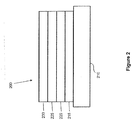
- FIG. 2 shows an inverted OLED 200.
- the device includes a substrate 210, a cathode 215, an emissive layer 220, a hole transport layer 225, and an anode 230.
- Device 200 may be fabricated by depositing the layers described, in order. Because the most common OLED configuration has a cathode disposed over the anode, and device 200 has cathode 215 disposed under anode 230, device 200 may be referred to as an "inverted" OLED. Materials similar to those described with respect to device 100 may be used in the corresponding layers of device 200.
- FIG. 2 provides one example of how some layers may be omitted from the structure of device 100.
- FIGS. 1 and 2 The simple layered structure illustrated in FIGS. 1 and 2 is provided by way of non-limiting example, and it is understood that embodiments of the invention may be used in connection with a wide variety of other structures.
- the specific materials and structures described are exemplary in nature, and other materials and structures may be used.
- Functional OLEDs may be achieved by combining the various layers described in different ways, or layers may be omitted entirely, based on design, performance, and cost factors. Other layers not specifically described may also be included. Materials other than those specifically described may be used. Although many of the examples provided herein describe various layers as comprising a single material, it is understood that combinations of materials, such as a mixture of host and dopant, or more generally a mixture, may be used. Also, the layers may have various sublayers.
- hole transport layer 225 transports holes and injects holes into emissive layer 220, and may be described as a hole transport layer or a hole injection layer.
- an OLED may be described as having an "organic layer" disposed between a cathode and an anode. This organic layer may comprise a single layer, or may further comprise multiple layers of different organic materials as described, for example, with respect to FIGS. 1 and 2 .
- OLEDs comprised of polymeric materials (PLEDs) such as disclosed in U.S. Pat. No. 5,247,190 to Friend et al. .
- PLEDs polymeric materials
- OLEDs having a single organic layer may be used.
- OLEDs may be stacked, for example as described in U.S. Pat. No. 5,707,745 to Forrest et al.
- the OLED structure may deviate from the simple layered structure illustrated in FIGS. 1 and 2 .
- the substrate may include an angled reflective surface to improve out-coupling, such as a mesa structure as described in U.S. Pat. No. 6,091,195 to Forrest et al. , and/or a pit structure as described in U.S. Pat. No. 5,834,893 to Bulovic et al. .
- any of the layers of the various embodiments may be deposited by any suitable method.
- preferred methods include thermal evaporation, ink-jet, such as described in U.S. Pat. Nos. 6,013,982 and 6,087,196 , organic vapor phase deposition (OVPD), such as described in U.S. Pat. No. 6,337,102 to Forrest et al. , and deposition by organic vapor jet printing (OVJP), such as described in U.S. Pat. No. 7,431,968 .
- OVPD organic vapor phase deposition
- OJP organic vapor jet printing
- Other suitable deposition methods include spin coating and other solution based processes. Solution based processes are preferably carried out in nitrogen or an inert atmosphere.
- preferred methods include thermal evaporation.
- Preferred patterning methods include deposition through a mask, cold welding such as described in U.S. Pat. Nos. 6,294,398 and 6,468,819 , and patterning associated with some of the deposition methods such as ink-jet and OVJD. Other methods may also be used.
- the materials to be deposited may be modified to make them compatible with a particular deposition method.
- substituents such as alkyl and aryl groups, branched or unbranched, and preferably containing at least 3 carbons, may be used in small molecules to enhance their ability to undergo solution processing. Substituents having 20 carbons or more may be used, and 3-20 carbons is a preferred range. Materials with asymmetric structures may have better solution processibility than those having symmetric structures, because asymmetric materials may have a lower tendency to recrystallize. Dendrimer substituents may be used to enhance the ability of small molecules to undergo solution processing.
- Devices fabricated in accordance with embodiments of the present invention may further optionally comprise a barrier layer.
- a barrier layer One purpose of the barrier layer is to protect the electrodes and organic layers from damaging exposure to harmful species in the environment including moisture, vapor and/or gases, etc.
- the barrier layer may be deposited over, under or next to a substrate, an electrode, or over any other parts of a device including an edge.
- the barrier layer may comprise a single layer, or multiple layers.
- the barrier layer may be formed by various known chemical vapor deposition techniques and may include compositions having a single phase as well as compositions having multiple phases. Any suitable material or combination of materials may be used for the barrier layer.
- the barrier layer may incorporate an inorganic or an organic compound or both.
- the preferred barrier layer comprises a mixture of a polymeric material and a non-polymeric material as described in U.S. Pat. No. 7,968,146 , PCT Pat. Application Nos. PCT/US2007/023098 and PCT/US2009/042829 .
- the aforesaid polymeric and non-polymeric materials comprising the barrier layer should be deposited under the same reaction conditions and/or at the same time.
- the weight ratio of polymeric to non-polymeric material may be in the range of 95:5 to 5:95.
- the polymeric material and the non-polymeric material may be created from the same precursor material.
- the mixture of a polymeric material and a non-polymeric material consists essentially of polymeric silicon and inorganic silicon.
- Devices fabricated in accordance with embodiments of the invention can be incorporated into a wide variety of electronic component modules (or units) that can be incorporated into a variety of electronic products or intermediate components. Examples of such electronic products or intermediate components include display screens, lighting devices such as discrete light source devices or lighting panels, etc. that can be utilized by the end-user product manufacturers. Such electronic component modules can optionally include the driving electronics and/or power source(s). Devices fabricated in accordance with embodiments of the invention can be incorporated into a wide variety of consumer products that have one or more of the electronic component modules (or units) incorporated therein. Such consumer products would include any kind of products that include one or more light source(s) and/or one or more of some type of visual displays.
- Some examples of such consumer products include flat panel displays, computer monitors, medical monitors, televisions, billboards, lights for interior or exterior illumination and/or signaling, heads-up displays, fully or partially transparent displays, flexible displays, laser printers, telephones, cell phones, tablets, phablets, personal digital assistants (PDAs), laptop computers, digital cameras, camcorders, viewfinders, micro-displays, 3-D displays, vehicles, a large area wall, theater or stadium screen, or a sign.
- PDAs personal digital assistants
- Various control mechanisms may be used to control devices fabricated in accordance with the present invention, including passive matrix and active matrix. Many of the devices are intended for use in a temperature range comfortable to humans, such as 18 degrees C. to 30 degrees C., and more preferably at room temperature (20-25 degrees C), but could be used outside this temperature range, for example, from -40 degree C to + 80 degree C.
- the materials and structures described herein may have applications in devices other than OLEDs.
- other optoelectronic devices such as organic solar cells and organic photodetectors may employ the materials and structures.
- organic devices such as organic transistors, may employ the materials and structures.
- halo includes fluorine, chlorine, bromine, and iodine.
- alkyl as used herein contemplates both straight and branched chain alkyl radicals.
- Preferred alkyl groups are those containing from one to fifteen carbon atoms and includes methyl, ethyl, propyl, isopropyl, butyl, isobutyl, tert-butyl, and the like. Additionally, the alkyl group may be optionally substituted.
- cycloalkyl as used herein contemplates cyclic alkyl radicals.
- Preferred cycloalkyl groups are those containing 3 to 7 carbon atoms and includes cyclopropyl, cyclopentyl, cyclohexyl, and the like. Additionally, the cycloalkyl group may be optionally substituted.
- alkenyl as used herein contemplates both straight and branched chain alkene radicals.
- Preferred alkenyl groups are those containing two to fifteen carbon atoms. Additionally, the alkenyl group may be optionally substituted.
- alkynyl as used herein contemplates both straight and branched chain alkyne radicals. Preferred alkynyl groups are those containing two to fifteen carbon atoms. Additionally, the alkynyl group may be optionally substituted.
- aralkyl or "arylalkyl” as used herein are used interchangeably and contemplate an alkyl group that has as a substituent an aromatic group. Additionally, the aralkyl group may be optionally substituted.
- heterocyclic group contemplates aromatic and non-aromatic cyclic radicals.
- Hetero-aromatic cyclic radicals also means heteroaryl.
- Preferred hetero-non-aromatic cyclic groups are those containing 3 or 7 ring atoms which includes at least one hetero atom, and includes cyclic amines such as morpholino, piperdino, pyrrolidino, and the like, and cyclic ethers, such as tetrahydrofuran, tetrahydropyran, and the like. Additionally, the heterocyclic group may be optionally substituted.
- aryl or "aromatic group” as used herein contemplates single-ring groups and polycyclic ring systems.
- the polycyclic rings may have two or more rings in which two carbons are common to two adjoining rings (the rings are "fused") wherein at least one of the rings is aromatic, e.g., the other rings can be cycloalkyls, cycloalkenyls, aryl, heterocycles, and/or heteroaryls.
- the aryl group may be optionally substituted, and may comprise, e.g., six to twenty carbon atoms.
- heteroaryl as used herein contemplates single-ring hetero-aromatic groups that may include from one to three heteroatoms and three to twenty carbon atoms, for example, pyrrole, furan, thiophene, imidazole, oxazole, thiazole, triazole, pyrazole, pyridine, pyrazine and pyrimidine, and the like.
- heteroaryl also includes polycyclic hetero-aromatic systems having two or more rings in which two atoms are common to two adjoining rings (the rings are "fused") wherein at least one of the rings is a heteroaryl, e.g., the other rings can be cycloalkyls, cycloalkenyls, aryl, heterocycles, and/or heteroaryls. Additionally, the heteroaryl group may be optionally substituted.
- alkyl, cycloalkyl, alkenyl, alkynyl, aralkyl, heterocyclic group, aryl, and heteroaryl may be optionally substituted with one or more substituents selected from the group consisting of hydrogen, deuterium, halogen, alkyl, cycloalkyl, heteroalkyl, arylalkyl, alkoxy, aryloxy, amino, cyclic amino, silyl, alkenyl, cycloalkenyl, heteroalkenyl, alkynyl, aryl, heteroaryl, acyl, carbonyl, carboxylic acid, ether, ester, nitrile, isonitrile, sulfanyl, sulfinyl, sulfonyl, phosphino, and combinations thereof.
- substituted indicates that a substituent other than H is bonded to the relevant position, such as carbon.
- substituent other than H such as carbon.
- R 1 is mono-substituted
- one R 1 must be other than H.
- R 1 is di-substituted
- two of R 1 must be other than H.
- R 1 is hydrogen for all available positions.
- aza-dibenzofuran i.e. aza-dibenzofuran, aza-dibenzothiophene, etc.
- azatriphenylene encompasses both dibenzo[ f , h ]quinoxaline and dibenzo[ f , h ]quinoline.
- a proposed mechanism for the decomposition of complexes that contain an uncoordinated nitrogen is an event where the uncoordinated nitrogen acts as a base by deprotonating a neighboring molecule, leading to non-emissive and potentially ionic reaction products. This event may happen in the excited state or in the presence of charged states found in the device environment.
- Multi-ring scaffolds such as the azaphenanthridine benzimidazole (APBI) ligand, may be useful to provide a functional site that can be substituted in order to address this decomposition mechanism.
- APBI azaphenanthridine benzimidazole
- the first approach places a steric group at the site in order to shield the lone pair of the uncoordinated nitrogen from exposure to protons on a neighboring molecule.
- Compounds 1-6 contain substitution designed to sterically shield the nitrogen from protonation:
- an aryl group is substituted on the ring opposite the uncoordinated nitrogen. Due to steric interaction, the ring is largely twisted out of plane, leading to a minimal increase in triplet energy. In addition, the plane of the aryl ring sits over the lone pair of the uncoordinated nitrogen, which should inhibit its exposure to nearby protons of neighboring molecules.
- the configuration of the aryl ring can be seen in the X-Ray crystal structure of Compound 1 ( Figure 3 ). However, an unexpected negative consequence of an aromatic substitution at this site is a decrease in PLQY.
- a second approach to improve stability comprises providing a hydrogen atom such that a static hydrogen bonding interaction is established between it and the lone pair of electrons on the uncoordinated nitrogen.
- This configuration serves to mitigate the reactivity of the lone pair, stabilizing the molecule from intermolecular degradation, and therefore improving the stability of the complex in a device.
- An exemplary azaphenanthridine benzimidazole (APBI) ligand is depicted below, wherein the hydrogen is defined as H*: It can be seen that H* points towards the lone pair of the nitrogen. It is believed that the proximity of the proton to the uncoordinated nitrogen is caused by steric repulsion between the methyl substituents on the isopropyl group and the ring system on the APBI.
- complexes can be designed to place a proton in close proximity to the lone pair of the nitrogen in order to form a static intramolecular hydrogen bond. Therefore if the lone pair of the nitrogen were to increase in basicity in the excited or charged state, then the lone pair and H* should be able to reversibly interact. On the other hand, a molecule without an intramolecular hydrogen bond could induce an irreversible degradation event by deprotonating a nearby molecule in the excited or charged state.
- the compounds of the present invention may be synthesized using techniques well-known in the art of organic synthesis.
- the starting materials and intermediates required for the synthesis may be obtained from commercial sources or synthesized according to methods known to those skilled in the art.
- the compound of the invention is a compound comprising a ligand L selected from the group A consisting of:
- the compound of the invention is a compound comprising a ligand L selected from the group A consisting of
- the compound of the invention is a compound comprising a ligand L selected from the group A consisting of:
- the metal M is selected from the group consisting of Ir, Rh, Re, Ru, Os, Pt, Au, and Cu. In another embodiment, M is Ir or Pt. In one embodiment, M is Ir. In another embodiment, M is Pt.
- the compounds of the invention include at least one intramolecular hydrogen bonding interaction to prevent deprotonation of neighboring molecules and to prevent protonation of an uncoordinated nitrogen.
- An exemplary intramolecular hydrogen bonding interaction can be found in scheme 1: Z 1 -H----Z 2 , scheme 1.
- Z 1 is carbon of alkyl
- Z 2 is one of X 1 to X 13 , and is nitrogen of pyridine.
- the location within the compound of Z 1 relative to Z 2 may be determined by the number of covalent bonds between Z 1 and Z 2 .
- Z 1 is at least 3 covalent bonds away from Z 2 .
- Z 1 is at least 4 covalent bonds away from Z 2 .
- Z 1 is at least 5 covalent bonds away from Z 2 .
- Z 1 is at least 6 covalent bonds away from Z 2 .
- An interaction between the hydrogen and Z 2 can be determined using any method known in the art.
- the interaction is determined using computational methods, such as by inspecting the Z 2 -H distance and spatial positioning in the minimized geometry.
- the distance between H and Z 2 ranges from 1.5 ⁇ to 2.4 ⁇ .
- the distance between H and Z 2 is equal to or less than 2.2 ⁇ .
- the distance between H and Z 2 is equal to or less than 2.16 ⁇ .
- the distance between H and Z 2 is equal to or less than 2.15 ⁇ .
- the interaction is determined using experimental methods, such as by measuring the 1 H (proton) NMR chemical shift of the hydrogen-bonding proton.
- the proton NMR chemical shift of H is shifted downfield by between 4.5 ppm and 7.0 ppm compared to the compound when Z 2 is carbon.
- the NMR chemical shift of H is shifted downfield by at least 1.3 ppm, more preferably at least 1.4 ppm, at least 1.5 ppm, at least 1.6 ppm, at least 1.7 ppm, at least 1.8 ppm, at least 1.9 ppm, or at least 2.0 ppm compared to the compound when Z 2 is carbon.
- the proton NMR chemical shift of H is shifted downfield by at least 1.3 ppm compared to the compound when Z 2 is carbon.
- the proton NMR chemical shift of H is shifted downfield by at least 1.4 ppm compared to the compound when Z 2 is carbon. In one embodiment, the proton NMR chemical shift of H is shifted downfield by between 30% and 60% compared to the compound when Z 2 is carbon. In some embodiments, the proton NMR chemical shift of H may be shifted downfield by at least 35%, at least 37%, at least 39%, at least 40%, at least 45%, or at least 50% compared to the compound when Z 2 is carbon. In one embodiment, the proton NMR chemical shift of H is shifted downfield by at least 35% compared to the compound when Z 2 is carbon. In another embodiment, the proton NMR chemical shift of H is shifted downfield by at least 37% compared to the compound when Z 2 is carbon
- the interaction is determined by measuring the emission of the first peak wavelength at the high energy end at room temperature and comparing it to the emission at a different temperature.
- room temperature refers to a temperature from about 20 °C to about 30 °C.
- compounds exhibiting an intramolecular hydrogen bonding interaction may also have an unusual triplet emission blue-shift in room temperature solution compared to the emission at a lower temperature.
- the compound has an room temperature emission blue shifted relative to 77K.
- the ligand L is selected from the group consisting of:
- the compound is homoleptic.
- a compound may be homoleptic when it comprises two or more ligands L, wherein the two or more ligands L are the same ligands.
- the compound is heteroleptic.
- a compound may be heteroleptic when it comprises two or more ligands L, wherein at least one of the ligands L is a different ligand from the other ligands L.
- the compound comprises at least one ligand L and at least one ligand L'.
- L' is a different ligand from L.
- L' is the same ligand as L.
- L is selected from group A. L' is not particularly limited.
- L' is a bidentate ligand.
- ligands L' may be optionally substituted, and any adjacent substituents may be optionally fused or joined to form a ring or form a multidentate ligand.
- L and L' are connected to form a multidentate ligand, such as a tridentate, tetradentate, pentadentate, or hexadentate ligand.
- L and L' are connected to form a tetradentate ligand.
- L and L' may be connected at one location or place to form a multidentate ligand, or L and L' may be connected at two or more locations or places to form a macrocyclic multidentate ligand.
- L and L' are connected at two places to form a macrocyclic tetradentate ligand.
- the compound has a formula of Ir(L) n (L') 3-n ; wherein L' is selected from group A; and wherein n is 1, 2, or 3.
- n is 1. In another embodiment, n is 2. In another embodiment, n is 3.
- the compound has a formula of Pt(L) m (L') 2-m ; wherein L' is selected from group A; and wherein m is 1, or 2.
- n is 1. In another embodiment, m is 2.
- the compound is selected from the group consisting of:
- the compound can be an emissive dopant.
- the compound can produce emissions via phosphorescence, fluorescence, thermally activated delayed fluorescence, i.e., TADF (also referred to as E-type delayed fluorescence), triplet-triplet annihilation, or combinations of these processes.
- TADF thermally activated delayed fluorescence
- a first device includes a first organic light emitting device, that includes an anode, a cathode, and an organic layer disposed between the anode and the cathode.
- the organic layer may include a host and a phosphorescent dopant.
- the emissive layer can include a compound comprising a ligand L, and its variations as described herein.
- the first device can be one or more of a consumer product, an electronic component module, an organic light-emitting device and a lighting panel.
- the organic layer can be an emissive layer and the compound can be an emissive dopant in some embodiments, while the compound can be a non-emissive dopant in other embodiments.
- the organic layer can be a charge transporting layer and the compound can be a charge transporting material in the organic layer in some embodiments.
- the organic layer can be a blocking layer and the compound can be a blocking material in the organic layer in some embodiments.
- the organic layer can also include a host.
- the host can include a metal complex.
- n can range from 1 to 10; and Ar 1 and Ar 2 can be independently selected from the group consisting of benzene, biphenyl, naphthalene, triphenylene, carbazole, and heteroaromatic analogs thereof.
- the host can be a compound comprising at least one chemical group selected from the group consisting of triphenylene, carbazole, dibenzothiphene, dibenzofuran, dibenzoselenophene, azatriphenylene, azacarbazole, aza-dibenzothiophene, aza-dibenzofuran, and aza-dibenzoselenophene.
- the host can include a metal complex.
- the host can be a specific compound selected from the group consisting of: and combinations thereof.
- a formulation that comprises a compound comprising a ligand L is described.
- the formulation can include one or more components selected from the group consisting of a solvent, a host, a hole injection material, hole transport material, and an electron transport layer material, disclosed herein.
- the materials described herein as useful for a particular layer in an organic light emitting device may be used in combination with a wide variety of other materials present in the device.
- emissive dopants disclosed herein may be used in conjunction with a wide variety of hosts, transport layers, blocking layers, injection layers, electrodes and other layers that may be present.
- the materials described or referred to below are non-limiting examples of materials that may be useful in combination with the compounds disclosed herein, and one of skill in the art can readily consult the literature to identify other materials that may be useful in combination.
- a hole injecting/transporting material to be used in the present invention is not particularly limited, and any compound may be used as long as the compound is typically used as a hole injecting/transporting material.
- the material include, but are not limited to: a phthalocyanine or porphyrin derivative; an aromatic amine derivative; an indolocarbazole derivative; a polymer containing fluorohydrocarbon; a polymer with conductivity dopants; a conducting polymer, such as PEDOT/PSS; a self-assembly monomer derived from compounds such as phosphonic acid and silane derivatives; a metal oxide derivative, such as MoO x ; a p-type semiconducting organic compound, such as 1,4,5,8,9,12-Hexaazatriphenylenehexacarbonitrile; a metal complex, and cross-linkable compounds.
- aromatic amine derivatives used in HIL or HTL include, but are not limited to the following general structures:
- Each of Ar 1 to Ar 9 is selected from the group consisting of aromatic hydrocarbon cyclic compounds such as benzene, biphenyl, triphenyl, triphenylene, naphthalene, anthracene, phenalene, phenanthrene, fluorene, pyrene, chrysene, perylene, and azulene; the group consisting of aromatic heterocyclic compounds such as dibenzothiophene, dibenzofuran, dibenzoselenophene, furan, thiophene, benzofuran, benzothiophene, benzoselenophene, carbazole, indolocarbazole, pyridylindole, pyrrolodipyridine, pyrazole, imidazole, triazole, oxazole, thiazole, oxadiazole, oxatriazole, dioxazole, thiadiazole, pyridine, pyridazine
- each Ar is further substituted by a substituent selected from the group consisting of hydrogen, deuterium, halide, alkyl, cycloalkyl, heteroalkyl, arylalkyl, alkoxy, aryloxy, amino, silyl, alkenyl, cycloalkenyl, heteroalkenyl, alkynyl, aryl, heteroaryl, acyl, carbonyl, carboxylic acids, ester, nitrile, isonitrile, sulfanyl, sulfinyl, sulfonyl, phosphino, and combinations thereof.
- a substituent selected from the group consisting of hydrogen, deuterium, halide, alkyl, cycloalkyl, heteroalkyl, arylalkyl, alkoxy, aryloxy, amino, silyl, alkenyl, cycloalkenyl, heteroalkenyl, alkynyl, aryl, heteroaryl, acy
- Ar 1 to Ar 9 is independently selected from the group consisting of: wherein k is an integer from 1 to 20; X 101 to X 108 is C (including CH) or N; Z 101 is NAr 1 , O, or S; Ar 1 has the same group defined above.
- metal complexes used in HIL or HTL include, but are not limited to the following general formula: wherein Met is a metal, which can have an atomic weight greater than 40; (Y 101 -Y 102 ) is a bidentate ligand, Y 101 and Y 102 are independently selected from C, N, O, P, and S; L 101 is an ancillary ligand; k' is an integer value from 1 to the maximum number of ligands that may be attached to the metal; and k'+k" is the maximum number of ligands that may be attached to the metal.
- (Y 101 -Y 102 ) is a 2-phenylpyridine derivative. In another aspect, (Y 101 -Y 102 ) is a carbene ligand. In another aspect, Met is selected from Ir, Pt, Os, and Zn. In a further aspect, the metal complex has a smallest oxidation potential in solution vs. Fc + /Fc couple less than about 0.6 V.
- the light emitting layer of the organic EL device of the present invention preferably contains at least a metal complex as light emitting material, and may contain a host material using the metal complex as a dopant material.
- the host material are not particularly limited, and any metal complexes or organic compounds may be used as long as the triplet energy of the host is larger than that of the dopant. While the Table below categorizes host materials as preferred for devices that emit various colors, any host material may be used with any dopant so long as the triplet criteria is satisfied.
- Examples of metal complexes used as host are preferred to have the following general formula: wherein Met is a metal; (Y 103 -Y 104 ) is a bidentate ligand, Y 103 and Y 104 are independently selected from C, N, O, P, and S; L 101 is an another ligand; k' is an integer value from 1 to the maximum number of ligands that may be attached to the metal; and k'+k" is the maximum number of ligands that may be attached to the metal.
- the metal complexes are: wherein (O-N) is a bidentate ligand, having metal coordinated to atoms O and N.
- Met is selected from Ir and Pt.
- (Y 103 -Y 104 ) is a carbene ligand.
- organic compounds used as host are selected from the group consisting of aromatic hydrocarbon cyclic compounds such as benzene, biphenyl, triphenyl, triphenylene, naphthalene, anthracene, phenalene, phenanthrene, fluorene, pyrene, chrysene, perylene, and azulene; the group consisting of aromatic heterocyclic compounds such as dibenzothiophene, dibenzofuran, dibenzoselenophene, furan, thiophene, benzofuran, benzothiophene, benzoselenophene, carbazole, indolocarbazole, pyridylindole, pyrrolodipyridine, pyrazole, imidazole, triazole, oxazole, thiazole, oxadiazole, oxatriazole, dioxazole, thiadiazole, pyridine, pyridazine,
- each group is further substituted by a substituent selected from the group consisting of hydrogen, deuterium, halide, alkyl, cycloalkyl, heteroalkyl, arylalkyl, alkoxy, aryloxy, amino, silyl, alkenyl, cycloalkenyl, heteroalkenyl, alkynyl, aryl, heteroaryl, acyl, carbonyl, carboxylic acids, ester, nitrile, isonitrile, sulfanyl, sulfinyl, sulfonyl, phosphino, and combinations thereof.
- a substituent selected from the group consisting of hydrogen, deuterium, halide, alkyl, cycloalkyl, heteroalkyl, arylalkyl, alkoxy, aryloxy, amino, silyl, alkenyl, cycloalkenyl, heteroalkenyl, alkynyl, aryl, heteroaryl, acy
- the host compound contains at least one of the following groups in the molecule:
- a hole blocking layer may be used to reduce the number of holes and/or excitons that leave the emissive layer.
- the presence of such a blocking layer in a device may result in substantially higher efficiencies as compared to a similar device lacking a blocking layer.
- a blocking layer may be used to confine emission to a desired region of an OLED.
- the compound used in the HBL contains the same molecule or the same functional groups used as the host described above.
- the compound used in the HBL contains at least one of the following groups in the molecule: wherein k is an integer from 1 to 20; L 101 is an another ligand, k' is an integer from 1 to 3.
- Electron transport layer may include a material capable of transporting electrons. Electron transport layer may be intrinsic (undoped), or doped. Doping may be used to enhance conductivity. Examples of the ETL material are not particularly limited, and any metal complexes or organic compounds may be used as long as they are typically used to transport electrons.
- the compound used in ETL contains at least one of the following groups in the molecule: wherein R 101 is selected from the group consisting of hydrogen, deuterium, halide, alkyl, cycloalkyl, heteroalkyl, arylalkyl, alkoxy, aryloxy, amino, silyl, alkenyl, cycloalkenyl, heteroalkenyl, alkynyl, aryl, heteroaryl, acyl, carbonyl, carboxylic acids, ester, nitrile, isonitrile, sulfanyl, sulfinyl, sulfonyl, phosphino, and combinations thereof, when it is aryl or heteroaryl, it has the similar definition as Ar's mentioned above.
- Ar 1 to Ar 3 has the similar definition as Ar's mentioned above.
- k is an integer from 1 to 20.
- X 101 to X 108 is selected from C (including CH) or N.
- the metal complexes used in ETL contains, but is not limited to, the following general formula: wherein (O-N) or (N-N) is a bidentate ligand, having metal coordinated to atoms O, N or N, N; L 101 is another ligand; k' is an integer value from 1 to the maximum number of ligands that may be attached to the metal.
- the hydrogen atoms can be partially or fully deuterated.
- any specifically listed substituent such as, without limitation, methyl, phenyl, pyridyl, etc. encompasses undeuterated, partially deuterated, and fully deuterated versions thereof.
- classes of substituents such as, without limitation, alkyl, aryl, cycloalkyl, heteroaryl, etc. also encompass undeuterated, partially deuterated, and fully deuterated versions thereof.
- hole injection materials In addition to and / or in combination with the materials disclosed herein, many hole injection materials, hole transporting materials, host materials, dopant materials, exiton/hole blocking layer materials, electron transporting and electron injecting materials may be used in an OLED.
- Non-limiting examples of the materials that may be used in an OLED in combination with materials disclosed herein are listed in Table A below. Table A lists non-limiting classes of materials, non-limiting examples of compounds for each class, and references that disclose the materials. TABLE A MATERIAL EXAMPLES OF MATERIAL PUBLICATIONS Hole injection materials Phthalocyanine and porphyrin compounds Appl. Phys. Lett. 69, 2160 (1996 ) Starburst triarylamines J. Lumin.
- Non-limiting examples of compounds of the invention that contain intramolecular hydrogen bonding include:
- FIG. 11 shows the emission spectra of Compound 7 in 2-methyl tetrahydrofuran (2-MeTHF) solvent at room temperature and 77 K.
- the room temperature emission was found to be significantly blue-shifted relative to 77 K, unlike any other Ir(APBI) 3 complex yet measured.
- this blue shift may be due to an inductive withdrawing effect, which reduces electron density on the covalently attached ring, thereby blue shifting the emission spectra.
Landscapes
- Chemical & Material Sciences (AREA)
- Organic Chemistry (AREA)
- Engineering & Computer Science (AREA)
- Materials Engineering (AREA)
- Crystallography & Structural Chemistry (AREA)
- Inorganic Chemistry (AREA)
- Physics & Mathematics (AREA)
- Optics & Photonics (AREA)
- Electroluminescent Light Sources (AREA)
- Luminescent Compositions (AREA)
Claims (16)
- Composé comprenant un ligand L choisi dans le groupe A constitué par :
 où X1 à X13 sont chacun indépendamment choisis dans le groupe constitué par carbone et azote ;où Ra, Rb, Rc, et Rd peuvent chacun représenter d'une monosubstitution au nombre maximal possible de substitutions, ou aucune substitution ;où Ra, Rb, Rc, et Rd sont chacun indépendamment choisis dans le groupe constitué par hydrogène, deutérium, halogénure, alkyle, cycloalkyle, hétéroalkyle, arylalkyle, alcoxy, aryloxy, amino, silyle, alcényle, cycloalcényle, hétéroalcényle, alcynyle, aryle, hétéroaryle, acyle, carbonyle, acides carboxyliques, ester, nitrile, isonitrile, sulfanyle, sulfinyle, sulfonyle, phosphino, et des combinaisons de ceux-ci ;où le ligand L est coordonné à un métal M choisi dans le groupe constitué par Ir, Rh, Re, Ru, Os, Pt, Au, et Cu ;où le ligand L est facultativement lié à d'autres ligands pour constituer un ligand tridentate, tétradentate, pentadentate ou hexadentate ;où le composé comprend au moins une interaction intramoléculaire de liaison hydrogène déterminée par la mesure du déplacement chimique en RMN 1H (proton) comme indiqué dans le schéma :
 où le déplacement chimique de H est décalé vers le bas d'au moins 1,3 ppm par rapport au composé lorsque Z2 est un carboneoù Z1 est un carbone d'alkyle ; etoù Z2 est l'un parmi X1 à X13, et est un azote de pyridine.
 - Composé selon la revendication 1, où dans le schéma 1, le déplacement chimique de H en RMN du proton est décalé vers le bas d'au moins 1,4 ppm par rapport au composé lorsque Z2 est un carbone.
- Composé selon la revendication 1 ou 2, où l'émission à température ambiante est décalée vers le bleu par rapport à 77 K.
- Composé selon l'une quelconque des revendications 1 à 3, où M est Ir ou Pt.
- Composé selon l'une quelconque des revendications 1 à 4, où Z1 est éloigné de Z2 d'au moins 4 liaisons covalentes.
- Composé selon l'une quelconque des revendications 1 à 3 ou 5, où le composé a une formule de Ir(L)n(L')3-n ;
où L' est choisi dans le groupe A ; et
où n vaut 1, 2, ou 3. - Composé selon l'une quelconque des revendications 1 à 3 ou 5, où le composé a une formule de Pt(L)m(L')2-m ;
où L' est choisi dans le groupe A ; et
où m vaut 1 ou 2. - Composé selon l'une quelconque des revendications 1 à 7, où le ligand L est choisi dans le groupe constitué par :

- Composé selon l'une quelconque des revendications 1 à 3, où le composé est choisi dans le groupe constitué par :

- Premier dispositif comprenant un premier dispositif électroluminescent organique, le premier dispositif électroluminescent organique comprenant :une anode ;une cathode ; etune couche organique, disposée entre l'anode et la cathode, comprenant un composé tel que défini dans l'une quelconque des revendications 1 à 9.
- Premier dispositif selon la revendication 10, où le premier dispositif est choisi dans le groupe constitué par un produit de consommation, un module de composant électronique, un dispositif électroluminescent organique, et un panneau d'éclairage.
- Premier dispositif selon les revendications 10 ou 11, où la couche organique est une couche émissive et le composé est un dopant émissif ou un dopant non émissif.
- Premier dispositif selon l'une quelconque des revendications 10 à 12, où la couche organique comprend en outre un hôte ; où l'hôte comprend un thiophène benzo-fusionné ou furane benzo-fusionné contenant du triphénylène ;
où tout substituant dans l'hôte est un substituant non fusionné choisi indépendamment dans le groupe constitué par CnH2n+1, OCnH2n+1, OAr1, N(CnH2n+1)2, N(Ar1)(Ar2), CH=CH-CnH2n+1, C≡CCnH2n+1, Ar1, Ar1-Ar2, CnH2n-Ar1, ou aucune substitution ;
où n va de 1 à 10 ; et
où Ar1 et Ar2 sont indépendamment choisis dans le groupe constitué par benzène, biphényle, naphtalène, triphénylène, carbazole, et des analogues hétéroaromatiques de ceux-ci. - Premier dispositif selon l'une quelconque des revendications 10 à 13, où la couche organique comprend en outre un hôte, où l'hôte comprend au moins un groupe chimique choisi dans le groupe constitué par triphénylène, carbazole, dibenzothiophène, dibenzofurane, dibenzosélénophène, azatriphénylène, azacarbazole, aza-dibenzothiophène, aza-dibenzofurane, et aza-dibenzosélénophène.
- Premier dispositif selon l'une quelconque des revendications 10 à 13, où la couche organique comprend en outre un hôte et l'hôte est choisi dans le groupe constitué par :


- Composé tel que défini dans l'une quelconque des revendications 1 à 9,
où dans le schéma 1, le déplacement chimique de H en RMN du proton est décalé vers le bas d'au moins 35 % par rapport au composé lorsque Z2 est un carbone.
Applications Claiming Priority (4)
| Application Number | Priority Date | Filing Date | Title |
|---|---|---|---|
| US201461979103P | 2014-04-14 | 2014-04-14 | |
| US201461991720P | 2014-05-12 | 2014-05-12 | |
| US14/672,034 US10008679B2 (en) | 2014-04-14 | 2015-03-27 | Organic electroluminescent materials and devices |
| EP15163179.3A EP2933259B1 (fr) | 2014-04-14 | 2015-04-10 | Matériaux et dispositifs électroluminescents organiques |
Related Parent Applications (2)
| Application Number | Title | Priority Date | Filing Date |
|---|---|---|---|
| EP15163179.3A Division-Into EP2933259B1 (fr) | 2014-04-14 | 2015-04-10 | Matériaux et dispositifs électroluminescents organiques |
| EP15163179.3A Division EP2933259B1 (fr) | 2014-04-14 | 2015-04-10 | Matériaux et dispositifs électroluminescents organiques |
Publications (2)
| Publication Number | Publication Date |
|---|---|
| EP3424934A1 EP3424934A1 (fr) | 2019-01-09 |
| EP3424934B1 true EP3424934B1 (fr) | 2021-07-14 |
Family
ID=52829007
Family Applications (2)
| Application Number | Title | Priority Date | Filing Date |
|---|---|---|---|
| EP15163179.3A Active EP2933259B1 (fr) | 2014-04-14 | 2015-04-10 | Matériaux et dispositifs électroluminescents organiques |
| EP18186898.5A Active EP3424934B1 (fr) | 2014-04-14 | 2015-04-10 | Matériaux et dispositifs électroluminescents organiques |
Family Applications Before (1)
| Application Number | Title | Priority Date | Filing Date |
|---|---|---|---|
| EP15163179.3A Active EP2933259B1 (fr) | 2014-04-14 | 2015-04-10 | Matériaux et dispositifs électroluminescents organiques |
Country Status (6)
| Country | Link |
|---|---|
| US (3) | US10008679B2 (fr) |
| EP (2) | EP2933259B1 (fr) |
| JP (2) | JP6684048B2 (fr) |
| KR (2) | KR102444007B1 (fr) |
| CN (2) | CN104974190B (fr) |
| TW (2) | TWI676629B (fr) |
Families Citing this family (19)
| Publication number | Priority date | Publication date | Assignee | Title |
|---|---|---|---|---|
| US9847498B2 (en) * | 2014-04-14 | 2017-12-19 | Universal Display Corporation | Organic electroluminescent materials and devices |
| US10008679B2 (en) * | 2014-04-14 | 2018-06-26 | Universal Display Corporation | Organic electroluminescent materials and devices |
| US10608186B2 (en) | 2016-09-14 | 2020-03-31 | Universal Display Corporation | Organic electroluminescent materials and devices |
| KR102149077B1 (ko) | 2016-09-23 | 2020-08-27 | 주식회사 엘지화학 | 유기 발광 소자 |
| KR101893310B1 (ko) | 2016-10-31 | 2018-08-29 | 주식회사 엘지화학 | 헤테로고리 화합물 및 이를 포함하는 유기 전자 소자 |
| US11152579B2 (en) * | 2016-12-28 | 2021-10-19 | Universal Display Corporation | Organic electroluminescent materials and devices |
| US11201293B2 (en) | 2017-02-28 | 2021-12-14 | Lg Chem, Ltd. | Heterocyclic compound and organic light-emitting device comprising same |
| WO2018182300A1 (fr) | 2017-03-27 | 2018-10-04 | 주식회사 엘지화학 | Composé hétérocyclique et dispositif électroluminescent organique le comprenant |
| US11832510B2 (en) | 2017-06-23 | 2023-11-28 | Universal Display Corporation | Organic electroluminescent materials and devices |
| US11802136B2 (en) | 2017-06-23 | 2023-10-31 | Universal Display Corporation | Organic electroluminescent materials and devices |
| US11814403B2 (en) | 2017-06-23 | 2023-11-14 | Universal Display Corporation | Organic electroluminescent materials and devices |
| CN107629786B (zh) * | 2017-10-24 | 2019-03-01 | 济南大学 | 2-甲基咪唑啉作为pH值和Fe3+双功能荧光探针的应用及其荧光探针 |
| KR102088095B1 (ko) | 2018-03-19 | 2020-03-11 | 주식회사 엘지화학 | 헤테로고리 화합물 및 이를 포함하는 유기 발광 소자 |
| JP2020158491A (ja) * | 2019-03-26 | 2020-10-01 | ユニバーサル ディスプレイ コーポレイション | 有機エレクトロルミネセンス材料及びデバイス |
| US11926638B2 (en) * | 2019-07-22 | 2024-03-12 | Universal Display Corporation | Organic electroluminescent materials and devices |
| WO2021016814A1 (fr) * | 2019-07-29 | 2021-02-04 | Guangdong Juhua Printed Display Technology Co., Ltd. | Composé d'or (iii) luminescent, son procédé de préparation et dispositif électroluminescent organique l'utilisant |
| KR20210066073A (ko) * | 2019-11-27 | 2021-06-07 | 삼성디스플레이 주식회사 | 유기금속 화합물 및 이를 포함한 유기 발광 소자 |
| KR20210112425A (ko) | 2020-03-04 | 2021-09-15 | 삼성디스플레이 주식회사 | 유기 전계 발광 소자 및 유기 전계 발광 소자용 유기 금속 화합물 |
| KR20210142032A (ko) | 2020-05-14 | 2021-11-24 | 삼성디스플레이 주식회사 | 유기금속 화합물 및 이를 포함한 유기 발광 소자 |
Citations (1)
| Publication number | Priority date | Publication date | Assignee | Title |
|---|---|---|---|---|
| WO2015027060A1 (fr) * | 2013-08-21 | 2015-02-26 | Arizona Board Of Regents On Behalf Of Arizona State University | Complexes métalliques tétradentates phosphorescents présentant des spectres d'émission modifiés |
Family Cites Families (170)
| Publication number | Priority date | Publication date | Assignee | Title |
|---|---|---|---|---|
| US4769292A (en) | 1987-03-02 | 1988-09-06 | Eastman Kodak Company | Electroluminescent device with modified thin film luminescent zone |
| GB8909011D0 (en) | 1989-04-20 | 1989-06-07 | Friend Richard H | Electroluminescent devices |
| US5061569A (en) | 1990-07-26 | 1991-10-29 | Eastman Kodak Company | Electroluminescent device with organic electroluminescent medium |
| DE69412567T2 (de) | 1993-11-01 | 1999-02-04 | Hodogaya Chemical Co., Ltd., Tokio/Tokyo | Aminverbindung und sie enthaltende Elektrolumineszenzvorrichtung |
| US5703436A (en) | 1994-12-13 | 1997-12-30 | The Trustees Of Princeton University | Transparent contacts for organic devices |
| US5707745A (en) | 1994-12-13 | 1998-01-13 | The Trustees Of Princeton University | Multicolor organic light emitting devices |
| US6939625B2 (en) | 1996-06-25 | 2005-09-06 | Nôrthwestern University | Organic light-emitting diodes and methods for assembly and enhanced charge injection |
| US5844363A (en) | 1997-01-23 | 1998-12-01 | The Trustees Of Princeton Univ. | Vacuum deposited, non-polymeric flexible organic light emitting devices |
| US6013982A (en) | 1996-12-23 | 2000-01-11 | The Trustees Of Princeton University | Multicolor display devices |
| US6091195A (en) | 1997-02-03 | 2000-07-18 | The Trustees Of Princeton University | Displays having mesa pixel configuration |
| US5834893A (en) | 1996-12-23 | 1998-11-10 | The Trustees Of Princeton University | High efficiency organic light emitting devices with light directing structures |
| US6303238B1 (en) | 1997-12-01 | 2001-10-16 | The Trustees Of Princeton University | OLEDs doped with phosphorescent compounds |
| US6337102B1 (en) | 1997-11-17 | 2002-01-08 | The Trustees Of Princeton University | Low pressure vapor phase deposition of organic thin films |
| US6087196A (en) | 1998-01-30 | 2000-07-11 | The Trustees Of Princeton University | Fabrication of organic semiconductor devices using ink jet printing |
| US6528187B1 (en) | 1998-09-08 | 2003-03-04 | Fuji Photo Film Co., Ltd. | Material for luminescence element and luminescence element using the same |
| US6097147A (en) | 1998-09-14 | 2000-08-01 | The Trustees Of Princeton University | Structure for high efficiency electroluminescent device |
| US6830828B2 (en) | 1998-09-14 | 2004-12-14 | The Trustees Of Princeton University | Organometallic complexes as phosphorescent emitters in organic LEDs |
| US6294398B1 (en) | 1999-11-23 | 2001-09-25 | The Trustees Of Princeton University | Method for patterning devices |
| US6458475B1 (en) | 1999-11-24 | 2002-10-01 | The Trustee Of Princeton University | Organic light emitting diode having a blue phosphorescent molecule as an emitter |
| KR100377321B1 (ko) | 1999-12-31 | 2003-03-26 | 주식회사 엘지화학 | 피-형 반도체 성질을 갖는 유기 화합물을 포함하는 전기소자 |
| US20020121638A1 (en) | 2000-06-30 | 2002-09-05 | Vladimir Grushin | Electroluminescent iridium compounds with fluorinated phenylpyridines, phenylpyrimidines, and phenylquinolines and devices made with such compounds |
| WO2002015645A1 (fr) | 2000-08-11 | 2002-02-21 | The Trustees Of Princeton University | Composes organometalliques et electrophosphorescence organique presentant un deplacement d'emission |
| US6579630B2 (en) | 2000-12-07 | 2003-06-17 | Canon Kabushiki Kaisha | Deuterated semiconducting organic compounds used for opto-electronic devices |
| JP3812730B2 (ja) | 2001-02-01 | 2006-08-23 | 富士写真フイルム株式会社 | 遷移金属錯体及び発光素子 |
| JP4307000B2 (ja) | 2001-03-08 | 2009-08-05 | キヤノン株式会社 | 金属配位化合物、電界発光素子及び表示装置 |
| JP4310077B2 (ja) | 2001-06-19 | 2009-08-05 | キヤノン株式会社 | 金属配位化合物及び有機発光素子 |
| ATE431970T1 (de) | 2001-06-20 | 2009-06-15 | Showa Denko Kk | Licht emittierendes material und organische leuchtdiode |
| US7071615B2 (en) | 2001-08-20 | 2006-07-04 | Universal Display Corporation | Transparent electrodes |
| US7250226B2 (en) | 2001-08-31 | 2007-07-31 | Nippon Hoso Kyokai | Phosphorescent compound, a phosphorescent composition and an organic light-emitting device |
| US7431968B1 (en) | 2001-09-04 | 2008-10-07 | The Trustees Of Princeton University | Process and apparatus for organic vapor jet deposition |
| US6835469B2 (en) | 2001-10-17 | 2004-12-28 | The University Of Southern California | Phosphorescent compounds and devices comprising the same |
| US7166368B2 (en) | 2001-11-07 | 2007-01-23 | E. I. Du Pont De Nemours And Company | Electroluminescent platinum compounds and devices made with such compounds |
| US6863997B2 (en) | 2001-12-28 | 2005-03-08 | The Trustees Of Princeton University | White light emitting OLEDs from combined monomer and aggregate emission |
| KR100691543B1 (ko) | 2002-01-18 | 2007-03-09 | 주식회사 엘지화학 | 새로운 전자 수송용 물질 및 이를 이용한 유기 발광 소자 |
| US20030230980A1 (en) | 2002-06-18 | 2003-12-18 | Forrest Stephen R | Very low voltage, high efficiency phosphorescent oled in a p-i-n structure |
| US7189989B2 (en) | 2002-08-22 | 2007-03-13 | Fuji Photo Film Co., Ltd. | Light emitting element |
| CN100439469C (zh) | 2002-08-27 | 2008-12-03 | 富士胶片株式会社 | 有机金属配位化合物、有机el元件及有机el显示器 |
| US6687266B1 (en) | 2002-11-08 | 2004-02-03 | Universal Display Corporation | Organic light emitting materials and devices |
| JP4365199B2 (ja) | 2002-12-27 | 2009-11-18 | 富士フイルム株式会社 | 有機電界発光素子 |
| JP4365196B2 (ja) | 2002-12-27 | 2009-11-18 | 富士フイルム株式会社 | 有機電界発光素子 |
| CN100387607C (zh) | 2003-03-24 | 2008-05-14 | 南加利福尼亚大学 | Ir的苯基-吡唑配合物 |
| US7090928B2 (en) | 2003-04-01 | 2006-08-15 | The University Of Southern California | Binuclear compounds |
| EP1717291A3 (fr) | 2003-04-15 | 2007-03-21 | Merck Patent GmbH | Mélanges de semi-conducteurs organiques aptes à l'émission et de matières matricielles, leur utilisation et composants électroniques contenant ces mélanges |
| US7029765B2 (en) | 2003-04-22 | 2006-04-18 | Universal Display Corporation | Organic light emitting devices having reduced pixel shrinkage |
| US20060186791A1 (en) | 2003-05-29 | 2006-08-24 | Osamu Yoshitake | Organic electroluminescent element |
| TW200504175A (en) | 2003-06-09 | 2005-02-01 | Hitachi Chemical Co Ltd | Metal coordination compound, polymer composition and organic electroluminescence element using the same |
| JP2005011610A (ja) | 2003-06-18 | 2005-01-13 | Nippon Steel Chem Co Ltd | 有機電界発光素子 |
| US20050025993A1 (en) | 2003-07-25 | 2005-02-03 | Thompson Mark E. | Materials and structures for enhancing the performance of organic light emitting devices |
| TWI390006B (zh) | 2003-08-07 | 2013-03-21 | Nippon Steel Chemical Co | Organic EL materials with aluminum clamps |
| DE10338550A1 (de) | 2003-08-19 | 2005-03-31 | Basf Ag | Übergangsmetallkomplexe mit Carbenliganden als Emitter für organische Licht-emittierende Dioden (OLEDs) |
| US20060269780A1 (en) | 2003-09-25 | 2006-11-30 | Takayuki Fukumatsu | Organic electroluminescent device |
| JP4822687B2 (ja) | 2003-11-21 | 2011-11-24 | 富士フイルム株式会社 | 有機電界発光素子 |
| US7332232B2 (en) | 2004-02-03 | 2008-02-19 | Universal Display Corporation | OLEDs utilizing multidentate ligand systems |
| KR100834327B1 (ko) | 2004-03-11 | 2008-06-02 | 미쓰비시 가가꾸 가부시키가이샤 | 전하 수송막용 조성물 및 이온 화합물, 이를 이용한 전하수송막 및 유기 전계 발광 장치, 및 유기 전계 발광 장치의제조 방법 및 전하 수송막의 제조 방법 |
| TW200531592A (en) | 2004-03-15 | 2005-09-16 | Nippon Steel Chemical Co | Organic electroluminescent device |
| JP4869565B2 (ja) | 2004-04-23 | 2012-02-08 | 富士フイルム株式会社 | 有機電界発光素子 |
| US7491823B2 (en) | 2004-05-18 | 2009-02-17 | The University Of Southern California | Luminescent compounds with carbene ligands |
| US7393599B2 (en) | 2004-05-18 | 2008-07-01 | The University Of Southern California | Luminescent compounds with carbene ligands |
| US7534505B2 (en) | 2004-05-18 | 2009-05-19 | The University Of Southern California | Organometallic compounds for use in electroluminescent devices |
| US7445855B2 (en) | 2004-05-18 | 2008-11-04 | The University Of Southern California | Cationic metal-carbene complexes |
| US7279704B2 (en) | 2004-05-18 | 2007-10-09 | The University Of Southern California | Complexes with tridentate ligands |
| US7154114B2 (en) | 2004-05-18 | 2006-12-26 | Universal Display Corporation | Cyclometallated iridium carbene complexes for use as hosts |
| WO2005123873A1 (fr) | 2004-06-17 | 2005-12-29 | Konica Minolta Holdings, Inc. | Mat)riau de dispositif )lectroluminescent organique, dispositif )lectroluminescent organique, )cran et dispositif d')clairage |
| JP5000496B2 (ja) | 2004-06-28 | 2012-08-15 | チバ ホールディング インコーポレーテッド | トリアゾールとベンゾトリアゾールのエレクトロルミネセンス金属錯体 |
| US20060008670A1 (en) | 2004-07-06 | 2006-01-12 | Chun Lin | Organic light emitting materials and devices |
| US7504657B2 (en) | 2004-07-23 | 2009-03-17 | Konica Minolta Holdings, Inc. | Organic electroluminescent element, display and illuminator |
| DE102004057072A1 (de) | 2004-11-25 | 2006-06-01 | Basf Ag | Verwendung von Übergangsmetall-Carbenkomplexen in organischen Licht-emittierenden Dioden (OLEDs) |
| JP2008526766A (ja) | 2004-12-30 | 2008-07-24 | イー・アイ・デュポン・ドウ・ヌムール・アンド・カンパニー | 有機金属錯体 |
| US8377571B2 (en) | 2005-02-04 | 2013-02-19 | Konica Minolta Holdings, Inc. | Material for organic electroluminescence element, organic electroluminescence element, display device and lighting device |
| KR100803125B1 (ko) | 2005-03-08 | 2008-02-14 | 엘지전자 주식회사 | 적색 인광 화합물 및 이를 사용한 유기전계발광소자 |
| WO2006098120A1 (fr) | 2005-03-16 | 2006-09-21 | Konica Minolta Holdings, Inc. | Materiau pour dispositif electroluminescent organique et dispositif electroluminescent organique |
| DE102005014284A1 (de) | 2005-03-24 | 2006-09-28 | Basf Ag | Verwendung von Verbindungen, welche aromatische oder heteroaromatische über Carbonyl-Gruppen enthaltende Gruppen verbundene Ringe enthalten, als Matrixmaterialien in organischen Leuchtdioden |
| JPWO2006103874A1 (ja) | 2005-03-29 | 2008-09-04 | コニカミノルタホールディングス株式会社 | 有機エレクトロルミネッセンス素子材料、有機エレクトロルミネッセンス素子、表示装置及び照明装置 |
| GB2439030B (en) | 2005-04-18 | 2011-03-02 | Konica Minolta Holdings Inc | Organic electroluminescent device, display and illuminating device |
| US7807275B2 (en) | 2005-04-21 | 2010-10-05 | Universal Display Corporation | Non-blocked phosphorescent OLEDs |
| JP4533796B2 (ja) | 2005-05-06 | 2010-09-01 | 富士フイルム株式会社 | 有機電界発光素子 |
| US9051344B2 (en) | 2005-05-06 | 2015-06-09 | Universal Display Corporation | Stability OLED materials and devices |
| EP1888708B1 (fr) | 2005-05-31 | 2012-11-21 | Universal Display Corporation | Hotes de triphenylene dans des diodes luminescentes phosphorescentes |
| US8709614B2 (en) | 2005-06-07 | 2014-04-29 | Nippon Steel & Sumikin Chemical Co., Ltd. | Organic metal complex and its use in organic electroluminescent device |
| WO2007002683A2 (fr) | 2005-06-27 | 2007-01-04 | E. I. Du Pont De Nemours And Company | Compositions polymeres electriquement conductrices |
| WO2007004380A1 (fr) | 2005-07-01 | 2007-01-11 | Konica Minolta Holdings, Inc. | Matériau pour élément électroluminescent organique, élément électroluminescent organique, dispositif d’affichage et équipement d’éclairage |
| WO2007028417A1 (fr) | 2005-09-07 | 2007-03-15 | Technische Universität Braunschweig | Émetteur triple comportant des anneaux à cinq éléments condensés |
| JP4887731B2 (ja) | 2005-10-26 | 2012-02-29 | コニカミノルタホールディングス株式会社 | 有機エレクトロルミネッセンス素子、表示装置及び照明装置 |
| US7993760B2 (en) | 2005-12-01 | 2011-08-09 | Nippon Steel Chemical Co., Ltd. | Compound for use in organic electroluminescent device and organic electroluminescent device |
| JPWO2007063796A1 (ja) | 2005-12-01 | 2009-05-07 | 新日鐵化学株式会社 | 有機電界発光素子 |
| KR20160030582A (ko) * | 2006-02-10 | 2016-03-18 | 유니버셜 디스플레이 코포레이션 | 시클로금속화 이미다조[1,2-f]페난트리딘 및 디이미다조[1,2-a:1'',2''-c]퀴나졸린 리간드, 및 이의 등전자성 및 벤즈고리화된 유사체의 금속 착체 |
| US8142909B2 (en) * | 2006-02-10 | 2012-03-27 | Universal Display Corporation | Blue phosphorescent imidazophenanthridine materials |
| JP4823730B2 (ja) | 2006-03-20 | 2011-11-24 | 新日鐵化学株式会社 | 発光層化合物及び有機電界発光素子 |
| EP2011790B1 (fr) | 2006-04-26 | 2016-06-29 | Idemitsu Kosan Co., Ltd. | Dérivé d'amine aromatique, élément électroluminescent organique employant ledit dérivé |
| WO2007132678A1 (fr) | 2006-05-11 | 2007-11-22 | Idemitsu Kosan Co., Ltd. | Dispositif électroluminescent organique |
| CN101461074B (zh) | 2006-06-02 | 2011-06-15 | 出光兴产株式会社 | 有机电致发光元件用材料及使用了它的有机电致发光元件 |
| KR20090040896A (ko) | 2006-08-23 | 2009-04-27 | 이데미쓰 고산 가부시키가이샤 | 방향족 아민 유도체 및 이들을 이용한 유기 전기발광 소자 |
| JP5589251B2 (ja) | 2006-09-21 | 2014-09-17 | コニカミノルタ株式会社 | 有機エレクトロルミネッセンス素子材料 |
| WO2008044723A1 (fr) | 2006-10-13 | 2008-04-17 | Konica Minolta Holdings, Inc. | Matériau de dispositif électroluminescent organique, dispositif électroluminescent organique, dispositif d'affichage et d'éclairage |
| US20080102223A1 (en) | 2006-11-01 | 2008-05-01 | Sigurd Wagner | Hybrid layers for use in coatings on electronic devices or other articles |
| US7968146B2 (en) | 2006-11-01 | 2011-06-28 | The Trustees Of Princeton University | Hybrid layers for use in coatings on electronic devices or other articles |
| EP2080762B1 (fr) | 2006-11-09 | 2016-09-14 | Nippon Steel & Sumikin Chemical Co., Ltd. | Composé pour un dispositif électroluminescent organique et dispositif électroluminescent organique |
| KR101347519B1 (ko) | 2006-11-24 | 2014-01-03 | 이데미쓰 고산 가부시키가이샤 | 방향족 아민 유도체 및 그것을 이용한 유기 전기발광 소자 |
| US8119255B2 (en) | 2006-12-08 | 2012-02-21 | Universal Display Corporation | Cross-linkable iridium complexes and organic light-emitting devices using the same |
| WO2008101842A1 (fr) | 2007-02-23 | 2008-08-28 | Basf Se | Complexes métalliques électroluminescents contenant des benzotriazoles |
| CN101687893B (zh) | 2007-04-26 | 2014-01-22 | 巴斯夫欧洲公司 | 含有吩噻嗪s-氧化物或吩噻嗪s,s-二氧化物基团的硅烷及其在oled中的用途 |
| EP2170911B1 (fr) | 2007-06-22 | 2018-11-28 | UDC Ireland Limited | Complexes de cu(i) luminescents |
| WO2009003898A1 (fr) | 2007-07-05 | 2009-01-08 | Basf Se | Diodes électroluminescentes organiques contenant des émetteurs de complexes carbène-métaux de transition et au moins un composé sélectionné parmi les disilylcarbazoles, disilyldibenzofurannes, disilyldibenzothiophènes, disilyldibenzophospholes, disilyldibenzothiophène-s-oxydes et di |
| US8021574B2 (en) | 2007-07-07 | 2011-09-20 | Idemitsu Kosan Co., Ltd. | Naphthalene derivative, material for organic electroluminescence device, and organic electroluminescence device using the same |
| US8779655B2 (en) | 2007-07-07 | 2014-07-15 | Idemitsu Kosan Co., Ltd. | Organic electroluminescence device and material for organic electroluminescence device |
| US20090045731A1 (en) | 2007-07-07 | 2009-02-19 | Idemitsu Kosan Co., Ltd. | Organic electroluminescence device and material for organic electroluminescence device |
| JP5473600B2 (ja) | 2007-07-07 | 2014-04-16 | 出光興産株式会社 | クリセン誘導体及びそれを用いた有機エレクトロルミネッセンス素子 |
| WO2009008205A1 (fr) | 2007-07-07 | 2009-01-15 | Idemitsu Kosan Co., Ltd. | Dispositif électroluminescent organique et matériau pour un dispositif électroluminescent organique |
| US8080658B2 (en) | 2007-07-10 | 2011-12-20 | Idemitsu Kosan Co., Ltd. | Material for organic electroluminescent element and organic electroluminescent element employing the same |
| US8114530B2 (en) | 2007-07-10 | 2012-02-14 | Idemitsu Kosan Co., Ltd. | Material for organic electroluminescence device and organic electroluminescence device utilizing the same |
| EP2173811A1 (fr) | 2007-07-27 | 2010-04-14 | E. I. du Pont de Nemours and Company | Dispersions aqueuses de polymères électriquement conducteurs contenant des nanoparticules minérales |
| KR20160086983A (ko) | 2007-08-08 | 2016-07-20 | 유니버셜 디스플레이 코포레이션 | 트리페닐렌기를 포함하는 벤조 융합 티오펜 또는 벤조 융합 푸란 화합물 |
| JP2009040728A (ja) | 2007-08-09 | 2009-02-26 | Canon Inc | 有機金属錯体及びこれを用いた有機発光素子 |
| US8383249B2 (en) * | 2007-10-04 | 2013-02-26 | Universal Display Corporation | Complexes with tridentate ligands |
| KR101642030B1 (ko) | 2007-10-17 | 2016-07-25 | 바스프 에스이 | 가교된 카르벤 리간드를 포함하는 전이 금속 착물 및 이의 용도 |
| US20090101870A1 (en) | 2007-10-22 | 2009-04-23 | E. I. Du Pont De Nemours And Company | Electron transport bi-layers and devices made with such bi-layers |
| JP5067114B2 (ja) | 2007-10-24 | 2012-11-07 | コニカミノルタホールディングス株式会社 | 有機エレクトロルミネッセンス素子材料、有機エレクトロルミネッセンス素子、表示装置及び照明装置 |
| US7914908B2 (en) | 2007-11-02 | 2011-03-29 | Global Oled Technology Llc | Organic electroluminescent device having an azatriphenylene derivative |
| DE102007053771A1 (de) | 2007-11-12 | 2009-05-14 | Merck Patent Gmbh | Organische Elektrolumineszenzvorrichtungen |
| EP2216313B1 (fr) | 2007-11-15 | 2013-02-20 | Idemitsu Kosan Co., Ltd. | Dérivé de benzochrysène et dispositif électroluminescent organique l'utilisant |
| EP2221897A4 (fr) | 2007-11-22 | 2012-08-08 | Idemitsu Kosan Co | Élement el organique et solution contenant un matériau el organique |
| JP5270571B2 (ja) | 2007-11-22 | 2013-08-21 | 出光興産株式会社 | 有機el素子 |
| WO2009073245A1 (fr) | 2007-12-06 | 2009-06-11 | Universal Display Corporation | Complexes organométalliques électroluminescents |
| US8221905B2 (en) | 2007-12-28 | 2012-07-17 | Universal Display Corporation | Carbazole-containing materials in phosphorescent light emitting diodes |
| WO2009085344A2 (fr) | 2007-12-28 | 2009-07-09 | Universal Display Corporation | Matériaux contenant du dibenzothiophène dans les diodes électroluminescentes phosphorescentes |
| US8471248B2 (en) | 2008-02-12 | 2013-06-25 | Basf Se | Electroluminiscent metal complexes with dibenzo[f,h] quinoxalines |
| CN104141112B (zh) | 2008-05-07 | 2017-09-19 | 普林斯顿大学理事会 | 用于电子器件或其他物品上的涂层中的混合层 |
| EP2311826B1 (fr) | 2008-11-03 | 2017-05-24 | LG Chem, Ltd. | Nouveau composé hétérocyclique contenant de l'azote et dispositif électronique organique utilisant un tel composé |
| JP5629970B2 (ja) | 2008-11-14 | 2014-11-26 | コニカミノルタ株式会社 | 有機エレクトロルミネッセンス素子、表示装置及び照明装置 |
| JP5412809B2 (ja) | 2008-11-21 | 2014-02-12 | コニカミノルタ株式会社 | イミダゾール化合物の製造方法 |
| JP5707665B2 (ja) | 2008-12-03 | 2015-04-30 | コニカミノルタ株式会社 | 有機エレクトロルミネッセンス素子、該素子を備えた照明装置及び表示装置 |
| US8709615B2 (en) | 2011-07-28 | 2014-04-29 | Universal Display Corporation | Heteroleptic iridium complexes as dopants |
| US8722205B2 (en) | 2009-03-23 | 2014-05-13 | Universal Display Corporation | Heteroleptic iridium complex |
| JP4523990B1 (ja) | 2009-08-31 | 2010-08-11 | 富士フイルム株式会社 | 有機電界発光素子用材料及び有機電界発光素子 |
| JP4551480B1 (ja) * | 2009-08-31 | 2010-09-29 | 富士フイルム株式会社 | 有機電界発光素子 |
| US8748011B2 (en) * | 2011-02-23 | 2014-06-10 | Universal Display Corporation | Ruthenium carbene complexes for OLED material |
| CN111732611B (zh) * | 2011-02-23 | 2022-08-23 | 通用显示公司 | 新型的四齿铂络合物 |
| US9315724B2 (en) * | 2011-06-14 | 2016-04-19 | Basf Se | Metal complexes comprising azabenzimidazole carbene ligands and the use thereof in OLEDs |
| KR101317495B1 (ko) | 2011-07-08 | 2013-10-15 | 주식회사 엘지화학 | 새로운 화합물 및 이를 이용한 유기 전자 소자 |
| TWI561527B (en) * | 2011-07-25 | 2016-12-11 | Universal Display Corp | Tetradentate platinum complexes |
| US9783564B2 (en) | 2011-07-25 | 2017-10-10 | Universal Display Corporation | Organic electroluminescent materials and devices |
| US9493698B2 (en) | 2011-08-31 | 2016-11-15 | Universal Display Corporation | Organic electroluminescent materials and devices |
| US9193745B2 (en) | 2011-11-15 | 2015-11-24 | Universal Display Corporation | Heteroleptic iridium complex |
| JP2013107558A (ja) | 2011-11-23 | 2013-06-06 | Tachi S Co Ltd | シート・トラック |
| KR101968371B1 (ko) | 2012-01-12 | 2019-04-11 | 유디씨 아일랜드 리미티드 | 디벤조[f,h]퀴녹살린과의 금속 착물 |
| US10211413B2 (en) * | 2012-01-17 | 2019-02-19 | Universal Display Corporation | Organic electroluminescent materials and devices |
| JP5870782B2 (ja) | 2012-03-15 | 2016-03-01 | コニカミノルタ株式会社 | 有機エレクトロルミネッセンス素子、有機エレクトロルミネッセンス素子の製造方法、照明装置及び表示装置 |
| EP3424936B1 (fr) * | 2012-08-07 | 2021-04-07 | Merck Patent GmbH | Complexe métallique |
| JP5403179B1 (ja) * | 2013-05-22 | 2014-01-29 | コニカミノルタ株式会社 | 電荷移動性薄膜 |
| WO2014189072A1 (fr) * | 2013-05-22 | 2014-11-27 | コニカミノルタ株式会社 | Dispositif électronique, élément électroluminescent organique, cellule solaire à film mince organique, et cellule solaire à colorant |
| KR102349659B1 (ko) * | 2013-06-10 | 2022-01-11 | 아리조나 보드 오브 리젠츠 온 비하프 오브 아리조나 스테이트 유니버시티 | 개질된 방출 스펙트럼을 갖는 인광성 네자리 금속 착물 |
| WO2015000955A1 (fr) * | 2013-07-02 | 2015-01-08 | Basf Se | Complexes de métal et de carbène de type diazabenzimidazole monosubstitué destinés à être utilisés dans des diodes électroluminescentes organiques |
| JP6804823B2 (ja) * | 2013-10-14 | 2020-12-23 | アリゾナ・ボード・オブ・リージェンツ・オン・ビハーフ・オブ・アリゾナ・ステイト・ユニバーシティーArizona Board of Regents on behalf of Arizona State University | 白金錯体およびデバイス |
| KR101546788B1 (ko) * | 2013-12-27 | 2015-08-24 | 희성소재 (주) | 헤테로고리 화합물 및 이를 이용한 유기발광소자 |
| US9847498B2 (en) * | 2014-04-14 | 2017-12-19 | Universal Display Corporation | Organic electroluminescent materials and devices |
| US10008679B2 (en) * | 2014-04-14 | 2018-06-26 | Universal Display Corporation | Organic electroluminescent materials and devices |
| US20170040538A1 (en) * | 2014-04-25 | 2017-02-09 | Sumitomo Chemical Company, Limited | Light-emitting device |
| US10403830B2 (en) * | 2014-05-08 | 2019-09-03 | Universal Display Corporation | Organic electroluminescent materials and devices |
| CN106661055B (zh) * | 2014-06-27 | 2019-09-13 | 喜星素材株式会社 | 杂环化合物以及使用该杂环化合物的有机发光器件 |
| US10672995B2 (en) * | 2014-07-24 | 2020-06-02 | Samsung Electronics Co., Ltd. | Organometallic compound and organic light-emitting device including the same |
| KR101772746B1 (ko) | 2014-08-12 | 2017-08-30 | 주식회사 엘지화학 | 유기 발광 소자 |
| CN107001324B (zh) * | 2014-10-29 | 2020-09-22 | Lt素材株式会社 | 含氮多环化合物及使用其的有机发光器件 |
| US9882151B2 (en) * | 2014-11-14 | 2018-01-30 | Universal Display Corporation | Organic electroluminescent materials and devices |
| CN107001336A (zh) * | 2014-12-11 | 2017-08-01 | 广州华睿光电材料有限公司 | 一种有机金属配合物、包含其的聚合物、混合物、组合物、有机电子器件及应用 |
| US9911928B2 (en) * | 2015-03-19 | 2018-03-06 | Universal Display Corporation | Organic electroluminescent materials and devices |
| KR20170030427A (ko) * | 2015-09-09 | 2017-03-17 | 주식회사 엘지화학 | 유기전계발광소자 |
| US11024808B2 (en) | 2015-12-29 | 2021-06-01 | Universal Display Corporation | Organic electroluminescent materials and devices |
| US20170324049A1 (en) * | 2016-05-05 | 2017-11-09 | Universal Display Corporation | Organic Electroluminescent Materials and Devices |
| US11152579B2 (en) | 2016-12-28 | 2021-10-19 | Universal Display Corporation | Organic electroluminescent materials and devices |
| US11765970B2 (en) | 2017-07-26 | 2023-09-19 | Universal Display Corporation | Organic electroluminescent materials and devices |
-
2015
- 2015-03-27 US US14/672,034 patent/US10008679B2/en active Active
- 2015-04-10 EP EP15163179.3A patent/EP2933259B1/fr active Active
- 2015-04-10 EP EP18186898.5A patent/EP3424934B1/fr active Active
- 2015-04-13 KR KR1020150051710A patent/KR102444007B1/ko active IP Right Grant
- 2015-04-13 TW TW104111836A patent/TWI676629B/zh active
- 2015-04-13 JP JP2015081348A patent/JP6684048B2/ja active Active
- 2015-04-13 TW TW108141401A patent/TWI724627B/zh active
- 2015-04-14 CN CN201510175589.3A patent/CN104974190B/zh active Active
- 2015-04-14 CN CN201910823646.2A patent/CN110606861A/zh active Pending
-
2018
- 2018-05-31 US US15/993,863 patent/US11005052B2/en active Active
-
2020
- 2020-03-27 JP JP2020057655A patent/JP6983270B2/ja active Active
-
2021
- 2021-03-24 US US17/211,357 patent/US11793066B2/en active Active
-
2022
- 2022-09-13 KR KR1020220114803A patent/KR20220131206A/ko not_active Application Discontinuation
Patent Citations (1)
| Publication number | Priority date | Publication date | Assignee | Title |
|---|---|---|---|---|
| WO2015027060A1 (fr) * | 2013-08-21 | 2015-02-26 | Arizona Board Of Regents On Behalf Of Arizona State University | Complexes métalliques tétradentates phosphorescents présentant des spectres d'émission modifiés |
Also Published As
| Publication number | Publication date |
|---|---|
| US11793066B2 (en) | 2023-10-17 |
| CN110606861A (zh) | 2019-12-24 |
| JP6983270B2 (ja) | 2021-12-17 |
| TW201602118A (zh) | 2016-01-16 |
| US20150295190A1 (en) | 2015-10-15 |
| JP6684048B2 (ja) | 2020-04-22 |
| EP2933259B1 (fr) | 2018-09-19 |
| TWI676629B (zh) | 2019-11-11 |
| EP2933259A1 (fr) | 2015-10-21 |
| JP2015221780A (ja) | 2015-12-10 |
| US11005052B2 (en) | 2021-05-11 |
| TW202003537A (zh) | 2020-01-16 |
| CN104974190B (zh) | 2019-09-27 |
| US10008679B2 (en) | 2018-06-26 |
| US20180287078A1 (en) | 2018-10-04 |
| EP3424934A1 (fr) | 2019-01-09 |
| JP2020117515A (ja) | 2020-08-06 |
| KR20150118549A (ko) | 2015-10-22 |
| CN104974190A (zh) | 2015-10-14 |
| US20210217972A1 (en) | 2021-07-15 |
| KR20220131206A (ko) | 2022-09-27 |
| KR102444007B1 (ko) | 2022-09-15 |
| TWI724627B (zh) | 2021-04-11 |
Similar Documents
| Publication | Publication Date | Title |
|---|---|---|
| KR102685764B1 (ko) | 유기 전계발광 물질 및 디바이스 | |
| EP3424934B1 (fr) | Matériaux et dispositifs électroluminescents organiques | |
| EP3007244B1 (fr) | Matériaux et dispositifs électroluminescents organiques | |
| EP2982729B1 (fr) | Matériaux et dispositifs électroluminescents organiques | |
| EP2927234B1 (fr) | Matériaux et dispositifs organiques électroluminescents | |
| EP2891659B1 (fr) | Matériaux et dispositifs électroluminescents organiques | |
| KR20240051905A (ko) | 유기 전계발광 물질 및 디바이스 | |
| KR102360548B1 (ko) | 유기 전계발광 물질 및 소자 | |
| EP3398953B1 (fr) | Matériaux et dispositifs électroluminescents organiques | |
| US20150295189A1 (en) | Organic Electroluminescent Materials and Devices | |
| EP3178832A1 (fr) | Complexes hétéroleptiques de carbène d'iridium et diode électroluminescente les utilisant | |
| KR20170133281A (ko) | 유기 전계발광 물질 및 디바이스 | |
| EP3447053B1 (fr) | Matériaux et dispositifs électroluminescents organiques | |
| KR102557211B1 (ko) | 유기 전계발광 물질 및 디바이스 | |
| KR20220100836A (ko) | 유기 전계발광 재료 및 소자 | |
| KR20200068567A (ko) | 유기 전계발광 물질 및 디바이스 | |
| KR20230112098A (ko) | 유기 전계발광 물질 및 디바이스 | |
| KR20200068554A (ko) | 유기 전계발광 물질 및 디바이스 | |
| EP3220441B1 (fr) | Matériaux et dispositifs électroluminescents organiques | |
| EP2963038B1 (fr) | Matériaux et dispositifs électroluminescents organiques | |
| KR20200030002A (ko) | 유기 전계발광 물질 및 디바이스 |
Legal Events
| Date | Code | Title | Description |
|---|---|---|---|
| PUAI | Public reference made under article 153(3) epc to a published international application that has entered the european phase |
Free format text: ORIGINAL CODE: 0009012 |
|
| STAA | Information on the status of an ep patent application or granted ep patent |
Free format text: STATUS: REQUEST FOR EXAMINATION WAS MADE |
|
| 17P | Request for examination filed |
Effective date: 20180801 |
|
| AC | Divisional application: reference to earlier application |
Ref document number: 2933259 Country of ref document: EP Kind code of ref document: P |
|
| AK | Designated contracting states |
Kind code of ref document: A1 Designated state(s): AL AT BE BG CH CY CZ DE DK EE ES FI FR GB GR HR HU IE IS IT LI LT LU LV MC MK MT NL NO PL PT RO RS SE SI SK SM TR |
|
| RAP1 | Party data changed (applicant data changed or rights of an application transferred) |
Owner name: UNIVERSAL DISPLAY CORPORATION |
|
| STAA | Information on the status of an ep patent application or granted ep patent |
Free format text: STATUS: EXAMINATION IS IN PROGRESS |
|
| 17Q | First examination report despatched |
Effective date: 20200616 |
|
| STAA | Information on the status of an ep patent application or granted ep patent |
Free format text: STATUS: EXAMINATION IS IN PROGRESS |
|
| GRAP | Despatch of communication of intention to grant a patent |
Free format text: ORIGINAL CODE: EPIDOSNIGR1 |
|
| STAA | Information on the status of an ep patent application or granted ep patent |
Free format text: STATUS: GRANT OF PATENT IS INTENDED |
|
| INTG | Intention to grant announced |
Effective date: 20210212 |
|
| RIN1 | Information on inventor provided before grant (corrected) |
Inventor name: SZIGETHY, GEZA Inventor name: BEERS, SCOTT Inventor name: CHEN, HSIAO-FAN Inventor name: BROOKS, JASON |
|
| GRAS | Grant fee paid |
Free format text: ORIGINAL CODE: EPIDOSNIGR3 |
|
| GRAA | (expected) grant |
Free format text: ORIGINAL CODE: 0009210 |
|
| STAA | Information on the status of an ep patent application or granted ep patent |
Free format text: STATUS: THE PATENT HAS BEEN GRANTED |
|
| AC | Divisional application: reference to earlier application |
Ref document number: 2933259 Country of ref document: EP Kind code of ref document: P |
|
| AK | Designated contracting states |
Kind code of ref document: B1 Designated state(s): AL AT BE BG CH CY CZ DE DK EE ES FI FR GB GR HR HU IE IS IT LI LT LU LV MC MK MT NL NO PL PT RO RS SE SI SK SM TR |
|
| REG | Reference to a national code |
Ref country code: GB Ref legal event code: FG4D |
|
| REG | Reference to a national code |
Ref country code: IE Ref legal event code: FG4D |
|
| REG | Reference to a national code |
Ref country code: DE Ref legal event code: R096 Ref document number: 602015071400 Country of ref document: DE |
|
| REG | Reference to a national code |
Ref country code: AT Ref legal event code: REF Ref document number: 1410575 Country of ref document: AT Kind code of ref document: T Effective date: 20210815 |
|
| REG | Reference to a national code |
Ref country code: LT Ref legal event code: MG9D |
|
| REG | Reference to a national code |
Ref country code: NL Ref legal event code: MP Effective date: 20210714 |
|
| REG | Reference to a national code |
Ref country code: AT Ref legal event code: MK05 Ref document number: 1410575 Country of ref document: AT Kind code of ref document: T Effective date: 20210714 |
|
| PG25 | Lapsed in a contracting state [announced via postgrant information from national office to epo] |
Ref country code: NO Free format text: LAPSE BECAUSE OF FAILURE TO SUBMIT A TRANSLATION OF THE DESCRIPTION OR TO PAY THE FEE WITHIN THE PRESCRIBED TIME-LIMIT Effective date: 20211014 Ref country code: NL Free format text: LAPSE BECAUSE OF FAILURE TO SUBMIT A TRANSLATION OF THE DESCRIPTION OR TO PAY THE FEE WITHIN THE PRESCRIBED TIME-LIMIT Effective date: 20210714 Ref country code: PT Free format text: LAPSE BECAUSE OF FAILURE TO SUBMIT A TRANSLATION OF THE DESCRIPTION OR TO PAY THE FEE WITHIN THE PRESCRIBED TIME-LIMIT Effective date: 20211115 Ref country code: AT Free format text: LAPSE BECAUSE OF FAILURE TO SUBMIT A TRANSLATION OF THE DESCRIPTION OR TO PAY THE FEE WITHIN THE PRESCRIBED TIME-LIMIT Effective date: 20210714 Ref country code: BG Free format text: LAPSE BECAUSE OF FAILURE TO SUBMIT A TRANSLATION OF THE DESCRIPTION OR TO PAY THE FEE WITHIN THE PRESCRIBED TIME-LIMIT Effective date: 20211014 Ref country code: LT Free format text: LAPSE BECAUSE OF FAILURE TO SUBMIT A TRANSLATION OF THE DESCRIPTION OR TO PAY THE FEE WITHIN THE PRESCRIBED TIME-LIMIT Effective date: 20210714 Ref country code: SE Free format text: LAPSE BECAUSE OF FAILURE TO SUBMIT A TRANSLATION OF THE DESCRIPTION OR TO PAY THE FEE WITHIN THE PRESCRIBED TIME-LIMIT Effective date: 20210714 Ref country code: RS Free format text: LAPSE BECAUSE OF FAILURE TO SUBMIT A TRANSLATION OF THE DESCRIPTION OR TO PAY THE FEE WITHIN THE PRESCRIBED TIME-LIMIT Effective date: 20210714 Ref country code: HR Free format text: LAPSE BECAUSE OF FAILURE TO SUBMIT A TRANSLATION OF THE DESCRIPTION OR TO PAY THE FEE WITHIN THE PRESCRIBED TIME-LIMIT Effective date: 20210714 Ref country code: FI Free format text: LAPSE BECAUSE OF FAILURE TO SUBMIT A TRANSLATION OF THE DESCRIPTION OR TO PAY THE FEE WITHIN THE PRESCRIBED TIME-LIMIT Effective date: 20210714 Ref country code: ES Free format text: LAPSE BECAUSE OF FAILURE TO SUBMIT A TRANSLATION OF THE DESCRIPTION OR TO PAY THE FEE WITHIN THE PRESCRIBED TIME-LIMIT Effective date: 20210714 |
|
| PG25 | Lapsed in a contracting state [announced via postgrant information from national office to epo] |
Ref country code: PL Free format text: LAPSE BECAUSE OF FAILURE TO SUBMIT A TRANSLATION OF THE DESCRIPTION OR TO PAY THE FEE WITHIN THE PRESCRIBED TIME-LIMIT Effective date: 20210714 Ref country code: LV Free format text: LAPSE BECAUSE OF FAILURE TO SUBMIT A TRANSLATION OF THE DESCRIPTION OR TO PAY THE FEE WITHIN THE PRESCRIBED TIME-LIMIT Effective date: 20210714 Ref country code: GR Free format text: LAPSE BECAUSE OF FAILURE TO SUBMIT A TRANSLATION OF THE DESCRIPTION OR TO PAY THE FEE WITHIN THE PRESCRIBED TIME-LIMIT Effective date: 20211015 |
|
| REG | Reference to a national code |
Ref country code: DE Ref legal event code: R097 Ref document number: 602015071400 Country of ref document: DE |
|
| PG25 | Lapsed in a contracting state [announced via postgrant information from national office to epo] |
Ref country code: DK Free format text: LAPSE BECAUSE OF FAILURE TO SUBMIT A TRANSLATION OF THE DESCRIPTION OR TO PAY THE FEE WITHIN THE PRESCRIBED TIME-LIMIT Effective date: 20210714 |
|
| PLBE | No opposition filed within time limit |
Free format text: ORIGINAL CODE: 0009261 |
|
| STAA | Information on the status of an ep patent application or granted ep patent |
Free format text: STATUS: NO OPPOSITION FILED WITHIN TIME LIMIT |
|
| PG25 | Lapsed in a contracting state [announced via postgrant information from national office to epo] |
Ref country code: SM Free format text: LAPSE BECAUSE OF FAILURE TO SUBMIT A TRANSLATION OF THE DESCRIPTION OR TO PAY THE FEE WITHIN THE PRESCRIBED TIME-LIMIT Effective date: 20210714 Ref country code: SK Free format text: LAPSE BECAUSE OF FAILURE TO SUBMIT A TRANSLATION OF THE DESCRIPTION OR TO PAY THE FEE WITHIN THE PRESCRIBED TIME-LIMIT Effective date: 20210714 Ref country code: RO Free format text: LAPSE BECAUSE OF FAILURE TO SUBMIT A TRANSLATION OF THE DESCRIPTION OR TO PAY THE FEE WITHIN THE PRESCRIBED TIME-LIMIT Effective date: 20210714 Ref country code: EE Free format text: LAPSE BECAUSE OF FAILURE TO SUBMIT A TRANSLATION OF THE DESCRIPTION OR TO PAY THE FEE WITHIN THE PRESCRIBED TIME-LIMIT Effective date: 20210714 Ref country code: CZ Free format text: LAPSE BECAUSE OF FAILURE TO SUBMIT A TRANSLATION OF THE DESCRIPTION OR TO PAY THE FEE WITHIN THE PRESCRIBED TIME-LIMIT Effective date: 20210714 Ref country code: AL Free format text: LAPSE BECAUSE OF FAILURE TO SUBMIT A TRANSLATION OF THE DESCRIPTION OR TO PAY THE FEE WITHIN THE PRESCRIBED TIME-LIMIT Effective date: 20210714 |
|
| 26N | No opposition filed |
Effective date: 20220419 |
|
| PG25 | Lapsed in a contracting state [announced via postgrant information from national office to epo] |
Ref country code: IT Free format text: LAPSE BECAUSE OF FAILURE TO SUBMIT A TRANSLATION OF THE DESCRIPTION OR TO PAY THE FEE WITHIN THE PRESCRIBED TIME-LIMIT Effective date: 20210714 |
|
| REG | Reference to a national code |
Ref country code: CH Ref legal event code: PL |
|
| GBPC | Gb: european patent ceased through non-payment of renewal fee |
Effective date: 20220410 |
|
| REG | Reference to a national code |
Ref country code: BE Ref legal event code: MM Effective date: 20220430 |
|
| PG25 | Lapsed in a contracting state [announced via postgrant information from national office to epo] |
Ref country code: LU Free format text: LAPSE BECAUSE OF NON-PAYMENT OF DUE FEES Effective date: 20220410 Ref country code: MC Free format text: LAPSE BECAUSE OF FAILURE TO SUBMIT A TRANSLATION OF THE DESCRIPTION OR TO PAY THE FEE WITHIN THE PRESCRIBED TIME-LIMIT Effective date: 20210714 Ref country code: LI Free format text: LAPSE BECAUSE OF NON-PAYMENT OF DUE FEES Effective date: 20220430 Ref country code: GB Free format text: LAPSE BECAUSE OF NON-PAYMENT OF DUE FEES Effective date: 20220410 Ref country code: FR Free format text: LAPSE BECAUSE OF NON-PAYMENT OF DUE FEES Effective date: 20220430 Ref country code: CH Free format text: LAPSE BECAUSE OF NON-PAYMENT OF DUE FEES Effective date: 20220430 |
|
| PG25 | Lapsed in a contracting state [announced via postgrant information from national office to epo] |
Ref country code: BE Free format text: LAPSE BECAUSE OF NON-PAYMENT OF DUE FEES Effective date: 20220430 |
|
| PG25 | Lapsed in a contracting state [announced via postgrant information from national office to epo] |
Ref country code: IE Free format text: LAPSE BECAUSE OF NON-PAYMENT OF DUE FEES Effective date: 20220410 |
|
| P01 | Opt-out of the competence of the unified patent court (upc) registered |
Effective date: 20230501 |
|
| PG25 | Lapsed in a contracting state [announced via postgrant information from national office to epo] |
Ref country code: HU Free format text: LAPSE BECAUSE OF FAILURE TO SUBMIT A TRANSLATION OF THE DESCRIPTION OR TO PAY THE FEE WITHIN THE PRESCRIBED TIME-LIMIT; INVALID AB INITIO Effective date: 20150410 |
|
| PG25 | Lapsed in a contracting state [announced via postgrant information from national office to epo] |
Ref country code: MK Free format text: LAPSE BECAUSE OF FAILURE TO SUBMIT A TRANSLATION OF THE DESCRIPTION OR TO PAY THE FEE WITHIN THE PRESCRIBED TIME-LIMIT Effective date: 20210714 Ref country code: CY Free format text: LAPSE BECAUSE OF FAILURE TO SUBMIT A TRANSLATION OF THE DESCRIPTION OR TO PAY THE FEE WITHIN THE PRESCRIBED TIME-LIMIT Effective date: 20210714 |
|
| PGFP | Annual fee paid to national office [announced via postgrant information from national office to epo] |
Ref country code: DE Payment date: 20240429 Year of fee payment: 10 |