EP2990503B1 - Method of forming metal film - Google Patents
Method of forming metal film Download PDFInfo
- Publication number
- EP2990503B1 EP2990503B1 EP15182652.6A EP15182652A EP2990503B1 EP 2990503 B1 EP2990503 B1 EP 2990503B1 EP 15182652 A EP15182652 A EP 15182652A EP 2990503 B1 EP2990503 B1 EP 2990503B1
- Authority
- EP
- European Patent Office
- Prior art keywords
- metal
- organic solvent
- mist
- acid
- film
- Prior art date
- Legal status (The legal status is an assumption and is not a legal conclusion. Google has not performed a legal analysis and makes no representation as to the accuracy of the status listed.)
- Active
Links
- 229910052751 metal Inorganic materials 0.000 title claims description 84
- 239000002184 metal Substances 0.000 title claims description 84
- 238000000034 method Methods 0.000 title claims description 39
- 239000012159 carrier gas Substances 0.000 claims description 44
- 239000003960 organic solvent Substances 0.000 claims description 43
- 239000003595 mist Substances 0.000 claims description 40
- 239000000243 solution Substances 0.000 claims description 28
- 239000002253 acid Substances 0.000 claims description 27
- XLYOFNOQVPJJNP-UHFFFAOYSA-N water Substances O XLYOFNOQVPJJNP-UHFFFAOYSA-N 0.000 claims description 27
- -1 amine compound Chemical class 0.000 claims description 25
- 239000002994 raw material Substances 0.000 claims description 25
- 239000007800 oxidant agent Substances 0.000 claims description 23
- 230000001590 oxidative effect Effects 0.000 claims description 22
- 239000010949 copper Substances 0.000 claims description 14
- RYGMFSIKBFXOCR-UHFFFAOYSA-N Copper Chemical compound [Cu] RYGMFSIKBFXOCR-UHFFFAOYSA-N 0.000 claims description 12
- 229910052802 copper Inorganic materials 0.000 claims description 12
- 239000007789 gas Substances 0.000 claims description 11
- 238000006243 chemical reaction Methods 0.000 claims description 9
- 239000000203 mixture Substances 0.000 claims description 8
- 238000000889 atomisation Methods 0.000 claims description 7
- 239000010948 rhodium Substances 0.000 claims description 7
- MHAJPDPJQMAIIY-UHFFFAOYSA-N Hydrogen peroxide Chemical compound OO MHAJPDPJQMAIIY-UHFFFAOYSA-N 0.000 claims description 6
- PXHVJJICTQNCMI-UHFFFAOYSA-N Nickel Chemical compound [Ni] PXHVJJICTQNCMI-UHFFFAOYSA-N 0.000 claims description 6
- KDLHZDBZIXYQEI-UHFFFAOYSA-N Palladium Chemical compound [Pd] KDLHZDBZIXYQEI-UHFFFAOYSA-N 0.000 claims description 6
- BASFCYQUMIYNBI-UHFFFAOYSA-N platinum Chemical compound [Pt] BASFCYQUMIYNBI-UHFFFAOYSA-N 0.000 claims description 6
- 229910052782 aluminium Inorganic materials 0.000 claims description 5
- XAGFODPZIPBFFR-UHFFFAOYSA-N aluminium Chemical compound [Al] XAGFODPZIPBFFR-UHFFFAOYSA-N 0.000 claims description 5
- 239000012298 atmosphere Substances 0.000 claims description 5
- 150000001875 compounds Chemical class 0.000 claims description 5
- 239000010931 gold Substances 0.000 claims description 5
- 239000011261 inert gas Substances 0.000 claims description 5
- 229910052703 rhodium Inorganic materials 0.000 claims description 5
- MHOVAHRLVXNVSD-UHFFFAOYSA-N rhodium atom Chemical compound [Rh] MHOVAHRLVXNVSD-UHFFFAOYSA-N 0.000 claims description 5
- 239000011651 chromium Substances 0.000 claims description 4
- 239000011572 manganese Substances 0.000 claims description 4
- 239000011259 mixed solution Substances 0.000 claims description 4
- 229910052737 gold Inorganic materials 0.000 claims description 3
- 238000010438 heat treatment Methods 0.000 claims description 3
- 229910052709 silver Inorganic materials 0.000 claims description 3
- VYZAMTAEIAYCRO-UHFFFAOYSA-N Chromium Chemical compound [Cr] VYZAMTAEIAYCRO-UHFFFAOYSA-N 0.000 claims description 2
- XEEYBQQBJWHFJM-UHFFFAOYSA-N Iron Chemical compound [Fe] XEEYBQQBJWHFJM-UHFFFAOYSA-N 0.000 claims description 2
- PWHULOQIROXLJO-UHFFFAOYSA-N Manganese Chemical compound [Mn] PWHULOQIROXLJO-UHFFFAOYSA-N 0.000 claims description 2
- ZOKXTWBITQBERF-UHFFFAOYSA-N Molybdenum Chemical compound [Mo] ZOKXTWBITQBERF-UHFFFAOYSA-N 0.000 claims description 2
- KJTLSVCANCCWHF-UHFFFAOYSA-N Ruthenium Chemical compound [Ru] KJTLSVCANCCWHF-UHFFFAOYSA-N 0.000 claims description 2
- BQCADISMDOOEFD-UHFFFAOYSA-N Silver Chemical compound [Ag] BQCADISMDOOEFD-UHFFFAOYSA-N 0.000 claims description 2
- 229910052804 chromium Inorganic materials 0.000 claims description 2
- 229910017052 cobalt Inorganic materials 0.000 claims description 2
- 239000010941 cobalt Substances 0.000 claims description 2
- GUTLYIVDDKVIGB-UHFFFAOYSA-N cobalt atom Chemical compound [Co] GUTLYIVDDKVIGB-UHFFFAOYSA-N 0.000 claims description 2
- 150000004696 coordination complex Chemical class 0.000 claims description 2
- PCHJSUWPFVWCPO-UHFFFAOYSA-N gold Chemical compound [Au] PCHJSUWPFVWCPO-UHFFFAOYSA-N 0.000 claims description 2
- 229910052748 manganese Inorganic materials 0.000 claims description 2
- 229910052750 molybdenum Inorganic materials 0.000 claims description 2
- 239000011733 molybdenum Substances 0.000 claims description 2
- 229910052759 nickel Inorganic materials 0.000 claims description 2
- 229910052763 palladium Inorganic materials 0.000 claims description 2
- 150000002978 peroxides Chemical class 0.000 claims description 2
- 229910052697 platinum Inorganic materials 0.000 claims description 2
- 229910052707 ruthenium Inorganic materials 0.000 claims description 2
- 239000012266 salt solution Substances 0.000 claims description 2
- 239000004332 silver Substances 0.000 claims description 2
- WFKWXMTUELFFGS-UHFFFAOYSA-N tungsten Chemical compound [W] WFKWXMTUELFFGS-UHFFFAOYSA-N 0.000 claims description 2
- 229910052721 tungsten Inorganic materials 0.000 claims description 2
- 239000010937 tungsten Substances 0.000 claims description 2
- 238000002604 ultrasonography Methods 0.000 claims description 2
- 125000003158 alcohol group Chemical group 0.000 claims 1
- 239000010408 film Substances 0.000 description 100
- 239000000758 substrate Substances 0.000 description 46
- 239000004065 semiconductor Substances 0.000 description 29
- OKKJLVBELUTLKV-UHFFFAOYSA-N Methanol Chemical compound OC OKKJLVBELUTLKV-UHFFFAOYSA-N 0.000 description 24
- 239000010410 layer Substances 0.000 description 24
- LFQSCWFLJHTTHZ-UHFFFAOYSA-N Ethanol Chemical compound CCO LFQSCWFLJHTTHZ-UHFFFAOYSA-N 0.000 description 21
- 239000013078 crystal Substances 0.000 description 10
- 238000010790 dilution Methods 0.000 description 10
- 239000012895 dilution Substances 0.000 description 10
- ZWEHNKRNPOVVGH-UHFFFAOYSA-N 2-Butanone Chemical compound CCC(C)=O ZWEHNKRNPOVVGH-UHFFFAOYSA-N 0.000 description 9
- QTBSBXVTEAMEQO-UHFFFAOYSA-N Acetic acid Chemical compound CC(O)=O QTBSBXVTEAMEQO-UHFFFAOYSA-N 0.000 description 9
- CSCPPACGZOOCGX-UHFFFAOYSA-N Acetone Chemical compound CC(C)=O CSCPPACGZOOCGX-UHFFFAOYSA-N 0.000 description 9
- IJGRMHOSHXDMSA-UHFFFAOYSA-N Atomic nitrogen Chemical compound N#N IJGRMHOSHXDMSA-UHFFFAOYSA-N 0.000 description 9
- RTZKZFJDLAIYFH-UHFFFAOYSA-N Diethyl ether Chemical compound CCOCC RTZKZFJDLAIYFH-UHFFFAOYSA-N 0.000 description 9
- XEKOWRVHYACXOJ-UHFFFAOYSA-N Ethyl acetate Chemical compound CCOC(C)=O XEKOWRVHYACXOJ-UHFFFAOYSA-N 0.000 description 9
- 230000001771 impaired effect Effects 0.000 description 9
- 230000015572 biosynthetic process Effects 0.000 description 8
- 238000000407 epitaxy Methods 0.000 description 8
- UHOVQNZJYSORNB-UHFFFAOYSA-N Benzene Chemical compound C1=CC=CC=C1 UHOVQNZJYSORNB-UHFFFAOYSA-N 0.000 description 6
- YMWUJEATGCHHMB-UHFFFAOYSA-N Dichloromethane Chemical compound ClCCl YMWUJEATGCHHMB-UHFFFAOYSA-N 0.000 description 6
- XTHFKEDIFFGKHM-UHFFFAOYSA-N Dimethoxyethane Chemical compound COCCOC XTHFKEDIFFGKHM-UHFFFAOYSA-N 0.000 description 6
- VEXZGXHMUGYJMC-UHFFFAOYSA-N Hydrochloric acid Chemical compound Cl VEXZGXHMUGYJMC-UHFFFAOYSA-N 0.000 description 6
- KFZMGEQAYNKOFK-UHFFFAOYSA-N Isopropanol Chemical compound CC(C)O KFZMGEQAYNKOFK-UHFFFAOYSA-N 0.000 description 6
- LRHPLDYGYMQRHN-UHFFFAOYSA-N N-Butanol Chemical compound CCCCO LRHPLDYGYMQRHN-UHFFFAOYSA-N 0.000 description 6
- DKGAVHZHDRPRBM-UHFFFAOYSA-N Tert-Butanol Chemical compound CC(C)(C)O DKGAVHZHDRPRBM-UHFFFAOYSA-N 0.000 description 6
- WYURNTSHIVDZCO-UHFFFAOYSA-N Tetrahydrofuran Chemical compound C1CCOC1 WYURNTSHIVDZCO-UHFFFAOYSA-N 0.000 description 6
- YXFVVABEGXRONW-UHFFFAOYSA-N Toluene Chemical compound CC1=CC=CC=C1 YXFVVABEGXRONW-UHFFFAOYSA-N 0.000 description 6
- DKPFZGUDAPQIHT-UHFFFAOYSA-N butyl acetate Chemical compound CCCCOC(C)=O DKPFZGUDAPQIHT-UHFFFAOYSA-N 0.000 description 6
- 150000002576 ketones Chemical class 0.000 description 6
- 238000005259 measurement Methods 0.000 description 6
- BDAGIHXWWSANSR-UHFFFAOYSA-N methanoic acid Natural products OC=O BDAGIHXWWSANSR-UHFFFAOYSA-N 0.000 description 6
- 229920000768 polyamine Polymers 0.000 description 6
- 238000002156 mixing Methods 0.000 description 5
- 238000001878 scanning electron micrograph Methods 0.000 description 5
- XKRFYHLGVUSROY-UHFFFAOYSA-N Argon Chemical compound [Ar] XKRFYHLGVUSROY-UHFFFAOYSA-N 0.000 description 4
- HEDRZPFGACZZDS-UHFFFAOYSA-N Chloroform Chemical compound ClC(Cl)Cl HEDRZPFGACZZDS-UHFFFAOYSA-N 0.000 description 4
- KRHYYFGTRYWZRS-UHFFFAOYSA-N Fluorane Chemical compound F KRHYYFGTRYWZRS-UHFFFAOYSA-N 0.000 description 4
- GLUUGHFHXGJENI-UHFFFAOYSA-N Piperazine Chemical compound C1CNCCN1 GLUUGHFHXGJENI-UHFFFAOYSA-N 0.000 description 4
- 239000000443 aerosol Substances 0.000 description 4
- 150000001735 carboxylic acids Chemical class 0.000 description 4
- MVPPADPHJFYWMZ-UHFFFAOYSA-N chlorobenzene Chemical compound ClC1=CC=CC=C1 MVPPADPHJFYWMZ-UHFFFAOYSA-N 0.000 description 4
- 238000000576 coating method Methods 0.000 description 4
- ZKXWKVVCCTZOLD-UHFFFAOYSA-N copper;4-hydroxypent-3-en-2-one Chemical compound [Cu].CC(O)=CC(C)=O.CC(O)=CC(C)=O ZKXWKVVCCTZOLD-UHFFFAOYSA-N 0.000 description 4
- 238000000151 deposition Methods 0.000 description 4
- XBDQKXXYIPTUBI-UHFFFAOYSA-N dimethylselenoniopropionate Natural products CCC(O)=O XBDQKXXYIPTUBI-UHFFFAOYSA-N 0.000 description 4
- 239000012212 insulator Substances 0.000 description 4
- VLKZOEOYAKHREP-UHFFFAOYSA-N n-Hexane Chemical compound CCCCCC VLKZOEOYAKHREP-UHFFFAOYSA-N 0.000 description 4
- 229910052757 nitrogen Inorganic materials 0.000 description 4
- VLTRZXGMWDSKGL-UHFFFAOYSA-N perchloric acid Chemical compound OCl(=O)(=O)=O VLTRZXGMWDSKGL-UHFFFAOYSA-N 0.000 description 4
- 238000004544 sputter deposition Methods 0.000 description 4
- VZGDMQKNWNREIO-UHFFFAOYSA-N tetrachloromethane Chemical compound ClC(Cl)(Cl)Cl VZGDMQKNWNREIO-UHFFFAOYSA-N 0.000 description 4
- 239000011882 ultra-fine particle Substances 0.000 description 4
- RYHBNJHYFVUHQT-UHFFFAOYSA-N 1,4-Dioxane Chemical compound C1COCCO1 RYHBNJHYFVUHQT-UHFFFAOYSA-N 0.000 description 3
- OSWFIVFLDKOXQC-UHFFFAOYSA-N 4-(3-methoxyphenyl)aniline Chemical compound COC1=CC=CC(C=2C=CC(N)=CC=2)=C1 OSWFIVFLDKOXQC-UHFFFAOYSA-N 0.000 description 3
- WEVYAHXRMPXWCK-UHFFFAOYSA-N Acetonitrile Chemical compound CC#N WEVYAHXRMPXWCK-UHFFFAOYSA-N 0.000 description 3
- ZAFNJMIOTHYJRJ-UHFFFAOYSA-N Diisopropyl ether Chemical compound CC(C)OC(C)C ZAFNJMIOTHYJRJ-UHFFFAOYSA-N 0.000 description 3
- PIICEJLVQHRZGT-UHFFFAOYSA-N Ethylenediamine Chemical compound NCCN PIICEJLVQHRZGT-UHFFFAOYSA-N 0.000 description 3
- WSFSSNUMVMOOMR-UHFFFAOYSA-N Formaldehyde Chemical compound O=C WSFSSNUMVMOOMR-UHFFFAOYSA-N 0.000 description 3
- NTIZESTWPVYFNL-UHFFFAOYSA-N Methyl isobutyl ketone Chemical compound CC(C)CC(C)=O NTIZESTWPVYFNL-UHFFFAOYSA-N 0.000 description 3
- UIHCLUNTQKBZGK-UHFFFAOYSA-N Methyl isobutyl ketone Natural products CCC(C)C(C)=O UIHCLUNTQKBZGK-UHFFFAOYSA-N 0.000 description 3
- BZLVMXJERCGZMT-UHFFFAOYSA-N Methyl tert-butyl ether Chemical compound COC(C)(C)C BZLVMXJERCGZMT-UHFFFAOYSA-N 0.000 description 3
- ZMXDDKWLCZADIW-UHFFFAOYSA-N N,N-Dimethylformamide Chemical compound CN(C)C=O ZMXDDKWLCZADIW-UHFFFAOYSA-N 0.000 description 3
- MUBZPKHOEPUJKR-UHFFFAOYSA-N Oxalic acid Chemical compound OC(=O)C(O)=O MUBZPKHOEPUJKR-UHFFFAOYSA-N 0.000 description 3
- OFOBLEOULBTSOW-UHFFFAOYSA-N Propanedioic acid Natural products OC(=O)CC(O)=O OFOBLEOULBTSOW-UHFFFAOYSA-N 0.000 description 3
- XBDQKXXYIPTUBI-UHFFFAOYSA-M Propionate Chemical compound CCC([O-])=O XBDQKXXYIPTUBI-UHFFFAOYSA-M 0.000 description 3
- 235000011054 acetic acid Nutrition 0.000 description 3
- 150000001298 alcohols Chemical class 0.000 description 3
- QVGXLLKOCUKJST-UHFFFAOYSA-N atomic oxygen Chemical compound [O] QVGXLLKOCUKJST-UHFFFAOYSA-N 0.000 description 3
- KRKNYBCHXYNGOX-UHFFFAOYSA-N citric acid Chemical compound OC(=O)CC(O)(C(O)=O)CC(O)=O KRKNYBCHXYNGOX-UHFFFAOYSA-N 0.000 description 3
- 150000002148 esters Chemical class 0.000 description 3
- 150000002170 ethers Chemical class 0.000 description 3
- 230000005669 field effect Effects 0.000 description 3
- 235000019253 formic acid Nutrition 0.000 description 3
- WBJINCZRORDGAQ-UHFFFAOYSA-N formic acid ethyl ester Natural products CCOC=O WBJINCZRORDGAQ-UHFFFAOYSA-N 0.000 description 3
- 150000004767 nitrides Chemical class 0.000 description 3
- 239000001301 oxygen Substances 0.000 description 3
- 229910052760 oxygen Inorganic materials 0.000 description 3
- 238000007747 plating Methods 0.000 description 3
- BDERNNFJNOPAEC-UHFFFAOYSA-N propan-1-ol Chemical compound CCCO BDERNNFJNOPAEC-UHFFFAOYSA-N 0.000 description 3
- 239000010453 quartz Substances 0.000 description 3
- 229910052594 sapphire Inorganic materials 0.000 description 3
- 239000010980 sapphire Substances 0.000 description 3
- 229910052710 silicon Inorganic materials 0.000 description 3
- 239000010703 silicon Substances 0.000 description 3
- VYPSYNLAJGMNEJ-UHFFFAOYSA-N silicon dioxide Inorganic materials O=[Si]=O VYPSYNLAJGMNEJ-UHFFFAOYSA-N 0.000 description 3
- YLQBMQCUIZJEEH-UHFFFAOYSA-N tetrahydrofuran Natural products C=1C=COC=1 YLQBMQCUIZJEEH-UHFFFAOYSA-N 0.000 description 3
- 239000010409 thin film Substances 0.000 description 3
- 238000007740 vapor deposition Methods 0.000 description 3
- MBVAQOHBPXKYMF-LNTINUHCSA-N (z)-4-hydroxypent-3-en-2-one;rhodium Chemical compound [Rh].C\C(O)=C\C(C)=O.C\C(O)=C\C(C)=O.C\C(O)=C\C(C)=O MBVAQOHBPXKYMF-LNTINUHCSA-N 0.000 description 2
- WSLDOOZREJYCGB-UHFFFAOYSA-N 1,2-Dichloroethane Chemical compound ClCCCl WSLDOOZREJYCGB-UHFFFAOYSA-N 0.000 description 2
- HXKKHQJGJAFBHI-UHFFFAOYSA-N 1-aminopropan-2-ol Chemical compound CC(O)CN HXKKHQJGJAFBHI-UHFFFAOYSA-N 0.000 description 2
- VILCJCGEZXAXTO-UHFFFAOYSA-N 2,2,2-tetramine Chemical compound NCCNCCNCCN VILCJCGEZXAXTO-UHFFFAOYSA-N 0.000 description 2
- ZVDSMYGTJDFNHN-UHFFFAOYSA-N 2,4,6-trimethylbenzene-1,3-diamine Chemical compound CC1=CC(C)=C(N)C(C)=C1N ZVDSMYGTJDFNHN-UHFFFAOYSA-N 0.000 description 2
- ICSNLGPSRYBMBD-UHFFFAOYSA-N 2-aminopyridine Chemical compound NC1=CC=CC=N1 ICSNLGPSRYBMBD-UHFFFAOYSA-N 0.000 description 2
- KDSNLYIMUZNERS-UHFFFAOYSA-N 2-methylpropanamine Chemical compound CC(C)CN KDSNLYIMUZNERS-UHFFFAOYSA-N 0.000 description 2
- RNLHGQLZWXBQNY-UHFFFAOYSA-N 3-(aminomethyl)-3,5,5-trimethylcyclohexan-1-amine Chemical compound CC1(C)CC(N)CC(C)(CN)C1 RNLHGQLZWXBQNY-UHFFFAOYSA-N 0.000 description 2
- CUYKNJBYIJFRCU-UHFFFAOYSA-N 3-aminopyridine Chemical compound NC1=CC=CN=C1 CUYKNJBYIJFRCU-UHFFFAOYSA-N 0.000 description 2
- UVLSCMIEPPWCHZ-UHFFFAOYSA-N 3-piperazin-1-ylpropan-1-amine Chemical compound NCCCN1CCNCC1 UVLSCMIEPPWCHZ-UHFFFAOYSA-N 0.000 description 2
- VVJKKWFAADXIJK-UHFFFAOYSA-N Allylamine Chemical compound NCC=C VVJKKWFAADXIJK-UHFFFAOYSA-N 0.000 description 2
- LSNNMFCWUKXFEE-UHFFFAOYSA-M Bisulfite Chemical compound OS([O-])=O LSNNMFCWUKXFEE-UHFFFAOYSA-M 0.000 description 2
- RPNUMPOLZDHAAY-UHFFFAOYSA-N Diethylenetriamine Chemical compound NCCNCCN RPNUMPOLZDHAAY-UHFFFAOYSA-N 0.000 description 2
- QUSNBJAOOMFDIB-UHFFFAOYSA-N Ethylamine Chemical compound CCN QUSNBJAOOMFDIB-UHFFFAOYSA-N 0.000 description 2
- ZHNUHDYFZUAESO-UHFFFAOYSA-N Formamide Chemical compound NC=O ZHNUHDYFZUAESO-UHFFFAOYSA-N 0.000 description 2
- VZCYOOQTPOCHFL-OWOJBTEDSA-N Fumaric acid Chemical compound OC(=O)\C=C\C(O)=O VZCYOOQTPOCHFL-OWOJBTEDSA-N 0.000 description 2
- GYHNNYVSQQEPJS-UHFFFAOYSA-N Gallium Chemical compound [Ga] GYHNNYVSQQEPJS-UHFFFAOYSA-N 0.000 description 2
- UFHFLCQGNIYNRP-UHFFFAOYSA-N Hydrogen Chemical compound [H][H] UFHFLCQGNIYNRP-UHFFFAOYSA-N 0.000 description 2
- BAVYZALUXZFZLV-UHFFFAOYSA-N Methylamine Chemical compound NC BAVYZALUXZFZLV-UHFFFAOYSA-N 0.000 description 2
- GRYLNZFGIOXLOG-UHFFFAOYSA-N Nitric acid Chemical compound O[N+]([O-])=O GRYLNZFGIOXLOG-UHFFFAOYSA-N 0.000 description 2
- KFSLWBXXFJQRDL-UHFFFAOYSA-N Peracetic acid Chemical compound CC(=O)OO KFSLWBXXFJQRDL-UHFFFAOYSA-N 0.000 description 2
- NBIIXXVUZAFLBC-UHFFFAOYSA-N Phosphoric acid Chemical compound OP(O)(O)=O NBIIXXVUZAFLBC-UHFFFAOYSA-N 0.000 description 2
- QAOWNCQODCNURD-UHFFFAOYSA-N Sulfuric acid Chemical compound OS(O)(=O)=O QAOWNCQODCNURD-UHFFFAOYSA-N 0.000 description 2
- XSTXAVWGXDQKEL-UHFFFAOYSA-N Trichloroethylene Chemical group ClC=C(Cl)Cl XSTXAVWGXDQKEL-UHFFFAOYSA-N 0.000 description 2
- DTQVDTLACAAQTR-UHFFFAOYSA-N Trifluoroacetic acid Chemical compound OC(=O)C(F)(F)F DTQVDTLACAAQTR-UHFFFAOYSA-N 0.000 description 2
- PNEYBMLMFCGWSK-UHFFFAOYSA-N aluminium oxide Inorganic materials [O-2].[O-2].[O-2].[Al+3].[Al+3] PNEYBMLMFCGWSK-UHFFFAOYSA-N 0.000 description 2
- 229910052786 argon Inorganic materials 0.000 description 2
- ZJRXSAYFZMGQFP-UHFFFAOYSA-N barium peroxide Chemical compound [Ba+2].[O-][O-] ZJRXSAYFZMGQFP-UHFFFAOYSA-N 0.000 description 2
- WGQKYBSKWIADBV-UHFFFAOYSA-N benzylamine Chemical compound NCC1=CC=CC=C1 WGQKYBSKWIADBV-UHFFFAOYSA-N 0.000 description 2
- 239000000872 buffer Substances 0.000 description 2
- 239000002738 chelating agent Substances 0.000 description 2
- 229910052593 corundum Inorganic materials 0.000 description 2
- PAFZNILMFXTMIY-UHFFFAOYSA-N cyclohexylamine Chemical compound NC1CCCCC1 PAFZNILMFXTMIY-UHFFFAOYSA-N 0.000 description 2
- 238000010586 diagram Methods 0.000 description 2
- JXTHNDFMNIQAHM-UHFFFAOYSA-N dichloroacetic acid Chemical compound OC(=O)C(Cl)Cl JXTHNDFMNIQAHM-UHFFFAOYSA-N 0.000 description 2
- 238000010304 firing Methods 0.000 description 2
- 229910052733 gallium Inorganic materials 0.000 description 2
- QZQVBEXLDFYHSR-UHFFFAOYSA-N gallium(III) oxide Inorganic materials O=[Ga]O[Ga]=O QZQVBEXLDFYHSR-UHFFFAOYSA-N 0.000 description 2
- 150000004820 halides Chemical class 0.000 description 2
- 150000008282 halocarbons Chemical class 0.000 description 2
- NAQMVNRVTILPCV-UHFFFAOYSA-N hexane-1,6-diamine Chemical compound NCCCCCCN NAQMVNRVTILPCV-UHFFFAOYSA-N 0.000 description 2
- 229930195733 hydrocarbon Natural products 0.000 description 2
- 150000002430 hydrocarbons Chemical class 0.000 description 2
- QWPPOHNGKGFGJK-UHFFFAOYSA-N hypochlorous acid Chemical compound ClO QWPPOHNGKGFGJK-UHFFFAOYSA-N 0.000 description 2
- 229910052738 indium Inorganic materials 0.000 description 2
- APFVFJFRJDLVQX-UHFFFAOYSA-N indium atom Chemical compound [In] APFVFJFRJDLVQX-UHFFFAOYSA-N 0.000 description 2
- 229910052809 inorganic oxide Inorganic materials 0.000 description 2
- JVTAAEKCZFNVCJ-UHFFFAOYSA-N lactic acid Chemical compound CC(O)C(O)=O JVTAAEKCZFNVCJ-UHFFFAOYSA-N 0.000 description 2
- 238000004519 manufacturing process Methods 0.000 description 2
- 239000000463 material Substances 0.000 description 2
- 229910044991 metal oxide Inorganic materials 0.000 description 2
- 150000004706 metal oxides Chemical class 0.000 description 2
- 239000002923 metal particle Substances 0.000 description 2
- VNWKTOKETHGBQD-UHFFFAOYSA-N methane Chemical compound C VNWKTOKETHGBQD-UHFFFAOYSA-N 0.000 description 2
- 150000007522 mineralic acids Chemical class 0.000 description 2
- 229910017604 nitric acid Inorganic materials 0.000 description 2
- LQNUZADURLCDLV-UHFFFAOYSA-N nitrobenzene Chemical compound [O-][N+](=O)C1=CC=CC=C1 LQNUZADURLCDLV-UHFFFAOYSA-N 0.000 description 2
- XNGIFLGASWRNHJ-UHFFFAOYSA-N phthalic acid Chemical compound OC(=O)C1=CC=CC=C1C(O)=O XNGIFLGASWRNHJ-UHFFFAOYSA-N 0.000 description 2
- 238000006068 polycondensation reaction Methods 0.000 description 2
- HIDKSOTTZRMUML-UHFFFAOYSA-M potassium;dodecanoate Chemical compound [K+].CCCCCCCCCCCC([O-])=O HIDKSOTTZRMUML-UHFFFAOYSA-M 0.000 description 2
- 235000019260 propionic acid Nutrition 0.000 description 2
- WGYKZJWCGVVSQN-UHFFFAOYSA-N propylamine Chemical compound CCCN WGYKZJWCGVVSQN-UHFFFAOYSA-N 0.000 description 2
- AOHJOMMDDJHIJH-UHFFFAOYSA-N propylenediamine Chemical compound CC(N)CN AOHJOMMDDJHIJH-UHFFFAOYSA-N 0.000 description 2
- IUVKMZGDUIUOCP-BTNSXGMBSA-N quinbolone Chemical compound O([C@H]1CC[C@H]2[C@H]3[C@@H]([C@]4(C=CC(=O)C=C4CC3)C)CC[C@@]21C)C1=CCCC1 IUVKMZGDUIUOCP-BTNSXGMBSA-N 0.000 description 2
- HBMJWWWQQXIZIP-UHFFFAOYSA-N silicon carbide Chemical compound [Si+]#[C-] HBMJWWWQQXIZIP-UHFFFAOYSA-N 0.000 description 2
- 229910010271 silicon carbide Inorganic materials 0.000 description 2
- 239000002904 solvent Substances 0.000 description 2
- 150000003460 sulfonic acids Chemical class 0.000 description 2
- FAGUFWYHJQFNRV-UHFFFAOYSA-N tetraethylenepentamine Chemical compound NCCNCCNCCNCCN FAGUFWYHJQFNRV-UHFFFAOYSA-N 0.000 description 2
- VZCYOOQTPOCHFL-UHFFFAOYSA-N trans-butenedioic acid Natural products OC(=O)C=CC(O)=O VZCYOOQTPOCHFL-UHFFFAOYSA-N 0.000 description 2
- UBOXGVDOUJQMTN-UHFFFAOYSA-N trichloroethylene Natural products ClCC(Cl)Cl UBOXGVDOUJQMTN-UHFFFAOYSA-N 0.000 description 2
- 229910001845 yogo sapphire Inorganic materials 0.000 description 2
- HMTSWYPNXFHGEP-UHFFFAOYSA-N (4-methylphenyl)methanamine Chemical compound CC1=CC=C(CN)C=C1 HMTSWYPNXFHGEP-UHFFFAOYSA-N 0.000 description 1
- YSEAGSCGERFGBL-UHFFFAOYSA-N (5-methylfuran-2-yl)methanamine Chemical compound CC1=CC=C(CN)O1 YSEAGSCGERFGBL-UHFFFAOYSA-N 0.000 description 1
- GEYOCULIXLDCMW-UHFFFAOYSA-N 1,2-phenylenediamine Chemical compound NC1=CC=CC=C1N GEYOCULIXLDCMW-UHFFFAOYSA-N 0.000 description 1
- WZCQRUWWHSTZEM-UHFFFAOYSA-N 1,3-phenylenediamine Chemical compound NC1=CC=CC(N)=C1 WZCQRUWWHSTZEM-UHFFFAOYSA-N 0.000 description 1
- FQUYSHZXSKYCSY-UHFFFAOYSA-N 1,4-diazepane Chemical compound C1CNCCNC1 FQUYSHZXSKYCSY-UHFFFAOYSA-N 0.000 description 1
- CBCKQZAAMUWICA-UHFFFAOYSA-N 1,4-phenylenediamine Chemical compound NC1=CC=C(N)C=C1 CBCKQZAAMUWICA-UHFFFAOYSA-N 0.000 description 1
- TXDNYIHPVKNPRJ-UHFFFAOYSA-N 1-(1h-imidazol-2-yl)propan-2-amine Chemical compound CC(N)CC1=NC=CN1 TXDNYIHPVKNPRJ-UHFFFAOYSA-N 0.000 description 1
- ZMESHQOXZMOOQQ-UHFFFAOYSA-N 1-(naphthalen-1-ylmethyl)naphthalene Chemical compound C1=CC=C2C(CC=3C4=CC=CC=C4C=CC=3)=CC=CC2=C1 ZMESHQOXZMOOQQ-UHFFFAOYSA-N 0.000 description 1
- XBWOPGDJMAJJDG-UHFFFAOYSA-N 1-cyclohexylethanamine Chemical compound CC(N)C1CCCCC1 XBWOPGDJMAJJDG-UHFFFAOYSA-N 0.000 description 1
- BMVXCPBXGZKUPN-UHFFFAOYSA-N 1-hexanamine Chemical compound CCCCCCN BMVXCPBXGZKUPN-UHFFFAOYSA-N 0.000 description 1
- OAGHHVORZFNXFM-UHFFFAOYSA-N 1-n,3-n-bis(3-aminopropyl)butane-1,3-diamine Chemical compound NCCCNC(C)CCNCCCN OAGHHVORZFNXFM-UHFFFAOYSA-N 0.000 description 1
- DBBZOURVEFUJEW-UHFFFAOYSA-N 1-n-dodecylpropane-1,2-diamine Chemical compound CCCCCCCCCCCCNCC(C)N DBBZOURVEFUJEW-UHFFFAOYSA-N 0.000 description 1
- DCYGAPKNVCQNOE-UHFFFAOYSA-N 2,2,2-triphenylacetic acid Chemical compound C=1C=CC=CC=1C(C=1C=CC=CC=1)(C(=O)O)C1=CC=CC=C1 DCYGAPKNVCQNOE-UHFFFAOYSA-N 0.000 description 1
- VOZKAJLKRJDJLL-UHFFFAOYSA-N 2,4-diaminotoluene Chemical compound CC1=CC=C(N)C=C1N VOZKAJLKRJDJLL-UHFFFAOYSA-N 0.000 description 1
- NSMWYRLQHIXVAP-UHFFFAOYSA-N 2,5-dimethylpiperazine Chemical compound CC1CNC(C)CN1 NSMWYRLQHIXVAP-UHFFFAOYSA-N 0.000 description 1
- RLYCRLGLCUXUPO-UHFFFAOYSA-N 2,6-diaminotoluene Chemical compound CC1=C(N)C=CC=C1N RLYCRLGLCUXUPO-UHFFFAOYSA-N 0.000 description 1
- IFNWESYYDINUHV-UHFFFAOYSA-N 2,6-dimethylpiperazine Chemical compound CC1CNCC(C)N1 IFNWESYYDINUHV-UHFFFAOYSA-N 0.000 description 1
- GIAFURWZWWWBQT-UHFFFAOYSA-N 2-(2-aminoethoxy)ethanol Chemical compound NCCOCCO GIAFURWZWWWBQT-UHFFFAOYSA-N 0.000 description 1
- VSPDYEHKAMKDNW-UHFFFAOYSA-N 2-(furan-2-ylmethylsulfanyl)ethanamine Chemical compound NCCSCC1=CC=CO1 VSPDYEHKAMKDNW-UHFFFAOYSA-N 0.000 description 1
- HZAXFHJVJLSVMW-UHFFFAOYSA-N 2-Aminoethan-1-ol Chemical compound NCCO HZAXFHJVJLSVMW-UHFFFAOYSA-N 0.000 description 1
- WOXFMYVTSLAQMO-UHFFFAOYSA-N 2-Pyridinemethanamine Chemical compound NCC1=CC=CC=N1 WOXFMYVTSLAQMO-UHFFFAOYSA-N 0.000 description 1
- RILZRCJGXSFXNE-UHFFFAOYSA-N 2-[4-(trifluoromethoxy)phenyl]ethanol Chemical compound OCCC1=CC=C(OC(F)(F)F)C=C1 RILZRCJGXSFXNE-UHFFFAOYSA-N 0.000 description 1
- WZFUQSJFWNHZHM-UHFFFAOYSA-N 2-[4-[2-(2,3-dihydro-1H-inden-2-ylamino)pyrimidin-5-yl]piperazin-1-yl]-1-(2,4,6,7-tetrahydrotriazolo[4,5-c]pyridin-5-yl)ethanone Chemical compound C1C(CC2=CC=CC=C12)NC1=NC=C(C=N1)N1CCN(CC1)CC(=O)N1CC2=C(CC1)NN=N2 WZFUQSJFWNHZHM-UHFFFAOYSA-N 0.000 description 1
- GEJJWYZZKKKSEV-UHFFFAOYSA-N 2-amino-1,2-diphenylethanol Chemical compound C=1C=CC=CC=1C(N)C(O)C1=CC=CC=C1 GEJJWYZZKKKSEV-UHFFFAOYSA-N 0.000 description 1
- BKMMTJMQCTUHRP-UHFFFAOYSA-N 2-aminopropan-1-ol Chemical compound CC(N)CO BKMMTJMQCTUHRP-UHFFFAOYSA-N 0.000 description 1
- KJJPLEZQSCZCKE-UHFFFAOYSA-N 2-aminopropane-1,3-diol Chemical compound OCC(N)CO KJJPLEZQSCZCKE-UHFFFAOYSA-N 0.000 description 1
- BPGIOCZAQDIBPI-UHFFFAOYSA-N 2-ethoxyethanamine Chemical compound CCOCCN BPGIOCZAQDIBPI-UHFFFAOYSA-N 0.000 description 1
- ASUDFOJKTJLAIK-UHFFFAOYSA-N 2-methoxyethanamine Chemical compound COCCN ASUDFOJKTJLAIK-UHFFFAOYSA-N 0.000 description 1
- JOMNTHCQHJPVAZ-UHFFFAOYSA-N 2-methylpiperazine Chemical compound CC1CNCCN1 JOMNTHCQHJPVAZ-UHFFFAOYSA-N 0.000 description 1
- CJNRGSHEMCMUOE-UHFFFAOYSA-N 2-piperidin-1-ylethanamine Chemical compound NCCN1CCCCC1 CJNRGSHEMCMUOE-UHFFFAOYSA-N 0.000 description 1
- ZAXCZCOUDLENMH-UHFFFAOYSA-N 3,3,3-tetramine Chemical compound NCCCNCCCNCCCN ZAXCZCOUDLENMH-UHFFFAOYSA-N 0.000 description 1
- ZGMQLPDXPUINCQ-UHFFFAOYSA-N 3,3,5-trimethylcyclohexan-1-amine Chemical compound CC1CC(N)CC(C)(C)C1 ZGMQLPDXPUINCQ-UHFFFAOYSA-N 0.000 description 1
- WGTASENVNYJZBK-UHFFFAOYSA-N 3,4,5-trimethoxyamphetamine Chemical compound COC1=CC(CC(C)N)=CC(OC)=C1OC WGTASENVNYJZBK-UHFFFAOYSA-N 0.000 description 1
- KRPRVQWGKLEFKN-UHFFFAOYSA-N 3-(3-aminopropoxy)propan-1-amine Chemical compound NCCCOCCCN KRPRVQWGKLEFKN-UHFFFAOYSA-N 0.000 description 1
- HPIXFUTWHVJYBG-UHFFFAOYSA-N 3-[1-(3-aminopropoxy)ethoxy]propan-1-amine Chemical compound NCCCOC(C)OCCCN HPIXFUTWHVJYBG-UHFFFAOYSA-N 0.000 description 1
- USNBVHYUYWSPNK-UHFFFAOYSA-N 3-[3-(3-aminopropoxy)-2,2-dimethylpropoxy]propan-1-amine Chemical compound NCCCOCC(C)(C)COCCCN USNBVHYUYWSPNK-UHFFFAOYSA-N 0.000 description 1
- ANOPCGQVRXJHHD-UHFFFAOYSA-N 3-[3-(3-aminopropyl)-2,4,8,10-tetraoxaspiro[5.5]undecan-9-yl]propan-1-amine Chemical compound C1OC(CCCN)OCC21COC(CCCN)OC2 ANOPCGQVRXJHHD-UHFFFAOYSA-N 0.000 description 1
- XBIUWALDKXACEA-UHFFFAOYSA-N 3-[bis(2,4-dioxopentan-3-yl)alumanyl]pentane-2,4-dione Chemical compound CC(=O)C(C(C)=O)[Al](C(C(C)=O)C(C)=O)C(C(C)=O)C(C)=O XBIUWALDKXACEA-UHFFFAOYSA-N 0.000 description 1
- KQIGMPWTAHJUMN-UHFFFAOYSA-N 3-aminopropane-1,2-diol Chemical compound NCC(O)CO KQIGMPWTAHJUMN-UHFFFAOYSA-N 0.000 description 1
- BMYNFMYTOJXKLE-UHFFFAOYSA-N 3-azaniumyl-2-hydroxypropanoate Chemical compound NCC(O)C(O)=O BMYNFMYTOJXKLE-UHFFFAOYSA-N 0.000 description 1
- VEGNPHHZDYJZQE-UHFFFAOYSA-N 3-dodecylimino-n-propylpropan-1-amine Chemical compound CCCCCCCCCCCCN=CCCNCCC VEGNPHHZDYJZQE-UHFFFAOYSA-N 0.000 description 1
- WTAZAHLROWIQRC-UHFFFAOYSA-N 3-ethylpyridin-2-amine Chemical compound CCC1=CC=CN=C1N WTAZAHLROWIQRC-UHFFFAOYSA-N 0.000 description 1
- XYUINKARGUCCQJ-UHFFFAOYSA-N 3-imino-n-propylpropan-1-amine Chemical compound CCCNCCC=N XYUINKARGUCCQJ-UHFFFAOYSA-N 0.000 description 1
- FAXDZWQIWUSWJH-UHFFFAOYSA-N 3-methoxypropan-1-amine Chemical compound COCCCN FAXDZWQIWUSWJH-UHFFFAOYSA-N 0.000 description 1
- RGDQRXPEZUNWHX-UHFFFAOYSA-N 3-methylpyridin-2-amine Chemical compound CC1=CC=CN=C1N RGDQRXPEZUNWHX-UHFFFAOYSA-N 0.000 description 1
- KKYSBGWCYXYOHA-UHFFFAOYSA-N 3-methylthiopropylamine Chemical compound CSCCCN KKYSBGWCYXYOHA-UHFFFAOYSA-N 0.000 description 1
- JMUCXULQKPWSTJ-UHFFFAOYSA-N 3-piperidin-1-ylpropan-1-amine Chemical compound NCCCN1CCCCC1 JMUCXULQKPWSTJ-UHFFFAOYSA-N 0.000 description 1
- FJIRTSVMONBPNB-UHFFFAOYSA-N 3-propylpyridin-2-amine Chemical compound CCCC1=CC=CN=C1N FJIRTSVMONBPNB-UHFFFAOYSA-N 0.000 description 1
- YBRVSVVVWCFQMG-UHFFFAOYSA-N 4,4'-diaminodiphenylmethane Chemical compound C1=CC(N)=CC=C1CC1=CC=C(N)C=C1 YBRVSVVVWCFQMG-UHFFFAOYSA-N 0.000 description 1
- BRBUBVKGJRPRRD-UHFFFAOYSA-N 4,6-dimethylpyridin-2-amine Chemical compound CC1=CC(C)=NC(N)=C1 BRBUBVKGJRPRRD-UHFFFAOYSA-N 0.000 description 1
- KSMVBYPXNKCPAJ-UHFFFAOYSA-N 4-Methylcyclohexylamine Chemical compound CC1CCC(N)CC1 KSMVBYPXNKCPAJ-UHFFFAOYSA-N 0.000 description 1
- NUKYPUAOHBNCPY-UHFFFAOYSA-N 4-aminopyridine Chemical compound NC1=CC=NC=C1 NUKYPUAOHBNCPY-UHFFFAOYSA-N 0.000 description 1
- RIUXWEGBWYUUEF-UHFFFAOYSA-N 4-bromo-2-cyclopropyl-1h-pyrrolo[2,3-b]pyridine Chemical compound C=1C=2C(Br)=CC=NC=2NC=1C1CC1 RIUXWEGBWYUUEF-UHFFFAOYSA-N 0.000 description 1
- FJKROLUGYXJWQN-UHFFFAOYSA-N 4-hydroxybenzoic acid Chemical compound OC(=O)C1=CC=C(O)C=C1 FJKROLUGYXJWQN-UHFFFAOYSA-N 0.000 description 1
- ORLGLBZRQYOWNA-UHFFFAOYSA-N 4-methylpyridin-2-amine Chemical compound CC1=CC=NC(N)=C1 ORLGLBZRQYOWNA-UHFFFAOYSA-N 0.000 description 1
- HUQGLWLBOCSVMD-UHFFFAOYSA-N 4-methylpyridine-2,6-diamine Chemical compound CC1=CC(N)=NC(N)=C1 HUQGLWLBOCSVMD-UHFFFAOYSA-N 0.000 description 1
- QUXLCYFNVNNRBE-UHFFFAOYSA-N 6-methylpyridin-2-amine Chemical compound CC1=CC=CC(N)=N1 QUXLCYFNVNNRBE-UHFFFAOYSA-N 0.000 description 1
- XYGFISRAXLLACA-UHFFFAOYSA-N 6-propan-2-ylpyridin-3-amine Chemical compound CC(C)C1=CC=C(N)C=N1 XYGFISRAXLLACA-UHFFFAOYSA-N 0.000 description 1
- PTKWYSNDTXDBIZ-UHFFFAOYSA-N 9,10-dioxoanthracene-1,2-disulfonic acid Chemical compound C1=CC=C2C(=O)C3=C(S(O)(=O)=O)C(S(=O)(=O)O)=CC=C3C(=O)C2=C1 PTKWYSNDTXDBIZ-UHFFFAOYSA-N 0.000 description 1
- JAJIPIAHCFBEPI-UHFFFAOYSA-N 9,10-dioxoanthracene-1-sulfonic acid Chemical compound O=C1C2=CC=CC=C2C(=O)C2=C1C=CC=C2S(=O)(=O)O JAJIPIAHCFBEPI-UHFFFAOYSA-N 0.000 description 1
- OUGMRQJTULXVDC-UHFFFAOYSA-N 9h-fluoren-9-amine Chemical compound C1=CC=C2C(N)C3=CC=CC=C3C2=C1 OUGMRQJTULXVDC-UHFFFAOYSA-N 0.000 description 1
- 239000004342 Benzoyl peroxide Substances 0.000 description 1
- OMPJBNCRMGITSC-UHFFFAOYSA-N Benzoylperoxide Chemical compound C=1C=CC=CC=1C(=O)OOC(=O)C1=CC=CC=C1 OMPJBNCRMGITSC-UHFFFAOYSA-N 0.000 description 1
- FEWJPZIEWOKRBE-JCYAYHJZSA-N Dextrotartaric acid Chemical compound OC(=O)[C@H](O)[C@@H](O)C(O)=O FEWJPZIEWOKRBE-JCYAYHJZSA-N 0.000 description 1
- 229920000877 Melamine resin Polymers 0.000 description 1
- FXHOOIRPVKKKFG-UHFFFAOYSA-N N,N-Dimethylacetamide Chemical compound CN(C)C(C)=O FXHOOIRPVKKKFG-UHFFFAOYSA-N 0.000 description 1
- OPKOKAMJFNKNAS-UHFFFAOYSA-N N-methylethanolamine Chemical compound CNCCO OPKOKAMJFNKNAS-UHFFFAOYSA-N 0.000 description 1
- CBENFWSGALASAD-UHFFFAOYSA-N Ozone Chemical compound [O-][O+]=O CBENFWSGALASAD-UHFFFAOYSA-N 0.000 description 1
- 229910019142 PO4 Inorganic materials 0.000 description 1
- WUGQZFFCHPXWKQ-UHFFFAOYSA-N Propanolamine Chemical compound NCCCO WUGQZFFCHPXWKQ-UHFFFAOYSA-N 0.000 description 1
- KDYFGRWQOYBRFD-UHFFFAOYSA-N Succinic acid Natural products OC(=O)CCC(O)=O KDYFGRWQOYBRFD-UHFFFAOYSA-N 0.000 description 1
- NINIDFKCEFEMDL-UHFFFAOYSA-N Sulfur Chemical compound [S] NINIDFKCEFEMDL-UHFFFAOYSA-N 0.000 description 1
- FEWJPZIEWOKRBE-UHFFFAOYSA-N Tartaric acid Natural products [H+].[H+].[O-]C(=O)C(O)C(O)C([O-])=O FEWJPZIEWOKRBE-UHFFFAOYSA-N 0.000 description 1
- 238000002441 X-ray diffraction Methods 0.000 description 1
- XZAHJRZBUWYCBM-UHFFFAOYSA-N [1-(aminomethyl)cyclohexyl]methanamine Chemical compound NCC1(CN)CCCCC1 XZAHJRZBUWYCBM-UHFFFAOYSA-N 0.000 description 1
- GKXVJHDEWHKBFH-UHFFFAOYSA-N [2-(aminomethyl)phenyl]methanamine Chemical compound NCC1=CC=CC=C1CN GKXVJHDEWHKBFH-UHFFFAOYSA-N 0.000 description 1
- 150000001334 alicyclic compounds Chemical class 0.000 description 1
- 125000002723 alicyclic group Chemical group 0.000 description 1
- 150000007824 aliphatic compounds Chemical class 0.000 description 1
- 125000001931 aliphatic group Chemical group 0.000 description 1
- 150000004996 alkyl benzenes Chemical class 0.000 description 1
- 229910000147 aluminium phosphate Inorganic materials 0.000 description 1
- 150000001408 amides Chemical class 0.000 description 1
- LHIJANUOQQMGNT-UHFFFAOYSA-N aminoethylethanolamine Chemical compound NCCNCCO LHIJANUOQQMGNT-UHFFFAOYSA-N 0.000 description 1
- IMUDHTPIFIBORV-UHFFFAOYSA-N aminoethylpiperazine Chemical compound NCCN1CCNCC1 IMUDHTPIFIBORV-UHFFFAOYSA-N 0.000 description 1
- 229950011175 aminopicoline Drugs 0.000 description 1
- ILFFFKFZHRGICY-UHFFFAOYSA-N anthracene-1-sulfonic acid Chemical compound C1=CC=C2C=C3C(S(=O)(=O)O)=CC=CC3=CC2=C1 ILFFFKFZHRGICY-UHFFFAOYSA-N 0.000 description 1
- 239000007864 aqueous solution Substances 0.000 description 1
- 150000001491 aromatic compounds Chemical class 0.000 description 1
- 125000003118 aryl group Chemical group 0.000 description 1
- 230000004888 barrier function Effects 0.000 description 1
- 235000019400 benzoyl peroxide Nutrition 0.000 description 1
- LZDHIQDKAYUDND-UHFFFAOYSA-N biphenylene-1,2-diamine Chemical compound C1=CC=C2C3=C(N)C(N)=CC=C3C2=C1 LZDHIQDKAYUDND-UHFFFAOYSA-N 0.000 description 1
- 239000008366 buffered solution Substances 0.000 description 1
- 230000003139 buffering effect Effects 0.000 description 1
- HQABUPZFAYXKJW-UHFFFAOYSA-N butan-1-amine Chemical compound CCCCN HQABUPZFAYXKJW-UHFFFAOYSA-N 0.000 description 1
- KDYFGRWQOYBRFD-NUQCWPJISA-N butanedioic acid Chemical compound O[14C](=O)CC[14C](O)=O KDYFGRWQOYBRFD-NUQCWPJISA-N 0.000 description 1
- 238000005229 chemical vapour deposition Methods 0.000 description 1
- FOCAUTSVDIKZOP-UHFFFAOYSA-N chloroacetic acid Chemical compound OC(=O)CCl FOCAUTSVDIKZOP-UHFFFAOYSA-N 0.000 description 1
- 235000015165 citric acid Nutrition 0.000 description 1
- 239000011247 coating layer Substances 0.000 description 1
- 239000000084 colloidal system Substances 0.000 description 1
- 238000004040 coloring Methods 0.000 description 1
- 239000002131 composite material Substances 0.000 description 1
- 239000004020 conductor Substances 0.000 description 1
- VXVVUHQULXCUPF-UHFFFAOYSA-N cycloheptanamine Chemical compound NC1CCCCCC1 VXVVUHQULXCUPF-UHFFFAOYSA-N 0.000 description 1
- AVKNGPAMCBSNSO-UHFFFAOYSA-N cyclohexylmethanamine Chemical compound NCC1CCCCC1 AVKNGPAMCBSNSO-UHFFFAOYSA-N 0.000 description 1
- HSOHBWMXECKEKV-UHFFFAOYSA-N cyclooctanamine Chemical compound NC1CCCCCCC1 HSOHBWMXECKEKV-UHFFFAOYSA-N 0.000 description 1
- NISGSNTVMOOSJQ-UHFFFAOYSA-N cyclopentanamine Chemical compound NC1CCCC1 NISGSNTVMOOSJQ-UHFFFAOYSA-N 0.000 description 1
- 239000008367 deionised water Substances 0.000 description 1
- 229910021641 deionized water Inorganic materials 0.000 description 1
- 230000008021 deposition Effects 0.000 description 1
- 150000004985 diamines Chemical class 0.000 description 1
- 229960005215 dichloroacetic acid Drugs 0.000 description 1
- KEIQPMUPONZJJH-UHFFFAOYSA-N dicyclohexylmethanediamine Chemical compound C1CCCCC1C(N)(N)C1CCCCC1 KEIQPMUPONZJJH-UHFFFAOYSA-N 0.000 description 1
- ZBCBWPMODOFKDW-UHFFFAOYSA-N diethanolamine Chemical compound OCCNCCO ZBCBWPMODOFKDW-UHFFFAOYSA-N 0.000 description 1
- AJNVQOSZGJRYEI-UHFFFAOYSA-N digallium;oxygen(2-) Chemical compound [O-2].[O-2].[O-2].[Ga+3].[Ga+3] AJNVQOSZGJRYEI-UHFFFAOYSA-N 0.000 description 1
- 229910001873 dinitrogen Inorganic materials 0.000 description 1
- MGHPNCMVUAKAIE-UHFFFAOYSA-N diphenylmethanamine Chemical compound C=1C=CC=CC=1C(N)C1=CC=CC=C1 MGHPNCMVUAKAIE-UHFFFAOYSA-N 0.000 description 1
- ZZTCPWRAHWXWCH-UHFFFAOYSA-N diphenylmethanediamine Chemical compound C=1C=CC=CC=1C(N)(N)C1=CC=CC=C1 ZZTCPWRAHWXWCH-UHFFFAOYSA-N 0.000 description 1
- LOKCTEFSRHRXRJ-UHFFFAOYSA-I dipotassium trisodium dihydrogen phosphate hydrogen phosphate dichloride Chemical compound P(=O)(O)(O)[O-].[K+].P(=O)(O)([O-])[O-].[Na+].[Na+].[Cl-].[K+].[Cl-].[Na+] LOKCTEFSRHRXRJ-UHFFFAOYSA-I 0.000 description 1
- 238000001035 drying Methods 0.000 description 1
- 238000005868 electrolysis reaction Methods 0.000 description 1
- 238000010894 electron beam technology Methods 0.000 description 1
- 229960004979 fampridine Drugs 0.000 description 1
- 239000000835 fiber Substances 0.000 description 1
- 238000001914 filtration Methods 0.000 description 1
- NVVZQXQBYZPMLJ-UHFFFAOYSA-N formaldehyde;naphthalene-1-sulfonic acid Chemical compound O=C.C1=CC=C2C(S(=O)(=O)O)=CC=CC2=C1 NVVZQXQBYZPMLJ-UHFFFAOYSA-N 0.000 description 1
- 239000013505 freshwater Substances 0.000 description 1
- 239000001530 fumaric acid Substances 0.000 description 1
- DDRPCXLAQZKBJP-UHFFFAOYSA-N furfurylamine Chemical compound NCC1=CC=CO1 DDRPCXLAQZKBJP-UHFFFAOYSA-N 0.000 description 1
- 229910001195 gallium oxide Inorganic materials 0.000 description 1
- 239000011521 glass Substances 0.000 description 1
- 150000002391 heterocyclic compounds Chemical class 0.000 description 1
- GNOIPBMMFNIUFM-UHFFFAOYSA-N hexamethylphosphoric triamide Chemical compound CN(C)P(=O)(N(C)C)N(C)C GNOIPBMMFNIUFM-UHFFFAOYSA-N 0.000 description 1
- XMBWDFGMSWQBCA-UHFFFAOYSA-N hydrogen iodide Chemical compound I XMBWDFGMSWQBCA-UHFFFAOYSA-N 0.000 description 1
- 229940071870 hydroiodic acid Drugs 0.000 description 1
- 125000002887 hydroxy group Chemical group [H]O* 0.000 description 1
- 150000002460 imidazoles Chemical class 0.000 description 1
- 239000012535 impurity Substances 0.000 description 1
- 230000006698 induction Effects 0.000 description 1
- 239000012770 industrial material Substances 0.000 description 1
- 150000002484 inorganic compounds Chemical class 0.000 description 1
- 229910010272 inorganic material Inorganic materials 0.000 description 1
- JJWLVOIRVHMVIS-UHFFFAOYSA-N isopropylamine Chemical compound CC(C)N JJWLVOIRVHMVIS-UHFFFAOYSA-N 0.000 description 1
- 239000004310 lactic acid Substances 0.000 description 1
- 235000014655 lactic acid Nutrition 0.000 description 1
- 239000002932 luster Substances 0.000 description 1
- 229940018564 m-phenylenediamine Drugs 0.000 description 1
- VZCYOOQTPOCHFL-UPHRSURJSA-N maleic acid Chemical compound OC(=O)\C=C/C(O)=O VZCYOOQTPOCHFL-UPHRSURJSA-N 0.000 description 1
- 239000011976 maleic acid Substances 0.000 description 1
- JDSHMPZPIAZGSV-UHFFFAOYSA-N melamine Chemical compound NC1=NC(N)=NC(N)=N1 JDSHMPZPIAZGSV-UHFFFAOYSA-N 0.000 description 1
- GBMDVOWEEQVZKZ-UHFFFAOYSA-N methanol;hydrate Chemical compound O.OC GBMDVOWEEQVZKZ-UHFFFAOYSA-N 0.000 description 1
- 239000012046 mixed solvent Substances 0.000 description 1
- DILRJUIACXKSQE-UHFFFAOYSA-N n',n'-dimethylethane-1,2-diamine Chemical compound CN(C)CCN DILRJUIACXKSQE-UHFFFAOYSA-N 0.000 description 1
- KMBPCQSCMCEPMU-UHFFFAOYSA-N n'-(3-aminopropyl)-n'-methylpropane-1,3-diamine Chemical compound NCCCN(C)CCCN KMBPCQSCMCEPMU-UHFFFAOYSA-N 0.000 description 1
- SCZVXVGZMZRGRU-UHFFFAOYSA-N n'-ethylethane-1,2-diamine Chemical compound CCNCCN SCZVXVGZMZRGRU-UHFFFAOYSA-N 0.000 description 1
- KFIGICHILYTCJF-UHFFFAOYSA-N n'-methylethane-1,2-diamine Chemical compound CNCCN KFIGICHILYTCJF-UHFFFAOYSA-N 0.000 description 1
- KGHYGBGIWLNFAV-UHFFFAOYSA-N n,n'-ditert-butylethane-1,2-diamine Chemical compound CC(C)(C)NCCNC(C)(C)C KGHYGBGIWLNFAV-UHFFFAOYSA-N 0.000 description 1
- LJAXTAOSOVPBQH-UHFFFAOYSA-N n-methylpiperidin-3-amine Chemical compound CNC1CCCNC1 LJAXTAOSOVPBQH-UHFFFAOYSA-N 0.000 description 1
- NGZYRKGJWYJGRS-UHFFFAOYSA-N n-methylpyrrolidin-3-amine Chemical compound CNC1CCNC1 NGZYRKGJWYJGRS-UHFFFAOYSA-N 0.000 description 1
- GPUMPJNVOBTUFM-UHFFFAOYSA-N naphthalene-1,2,3-trisulfonic acid Chemical compound C1=CC=C2C(S(O)(=O)=O)=C(S(O)(=O)=O)C(S(=O)(=O)O)=CC2=C1 GPUMPJNVOBTUFM-UHFFFAOYSA-N 0.000 description 1
- YZMHQCWXYHARLS-UHFFFAOYSA-N naphthalene-1,2-disulfonic acid Chemical compound C1=CC=CC2=C(S(O)(=O)=O)C(S(=O)(=O)O)=CC=C21 YZMHQCWXYHARLS-UHFFFAOYSA-N 0.000 description 1
- GOGZBMRXLADNEV-UHFFFAOYSA-N naphthalene-2,6-diamine Chemical compound C1=C(N)C=CC2=CC(N)=CC=C21 GOGZBMRXLADNEV-UHFFFAOYSA-N 0.000 description 1
- 150000002825 nitriles Chemical class 0.000 description 1
- RGHXWDVNBYKJQH-UHFFFAOYSA-N nitroacetic acid Chemical compound OC(=O)C[N+]([O-])=O RGHXWDVNBYKJQH-UHFFFAOYSA-N 0.000 description 1
- 239000012299 nitrogen atmosphere Substances 0.000 description 1
- 230000003287 optical effect Effects 0.000 description 1
- 150000002894 organic compounds Chemical class 0.000 description 1
- 150000001451 organic peroxides Chemical class 0.000 description 1
- 230000003204 osmotic effect Effects 0.000 description 1
- 235000006408 oxalic acid Nutrition 0.000 description 1
- YNOGYQAEJGADFJ-UHFFFAOYSA-N oxolan-2-ylmethanamine Chemical compound NCC1CCCO1 YNOGYQAEJGADFJ-UHFFFAOYSA-N 0.000 description 1
- 150000002989 phenols Chemical class 0.000 description 1
- 239000010452 phosphate Substances 0.000 description 1
- NBIIXXVUZAFLBC-UHFFFAOYSA-K phosphate Chemical compound [O-]P([O-])([O-])=O NBIIXXVUZAFLBC-UHFFFAOYSA-K 0.000 description 1
- 239000002953 phosphate buffered saline Substances 0.000 description 1
- 239000002504 physiological saline solution Substances 0.000 description 1
- RHPBLLCTOLJFPH-UHFFFAOYSA-N piperidin-2-ylmethanamine Chemical compound NCC1CCCCN1 RHPBLLCTOLJFPH-UHFFFAOYSA-N 0.000 description 1
- LTEKQAPRXFBRNN-UHFFFAOYSA-N piperidin-4-ylmethanamine Chemical compound NCC1CCNCC1 LTEKQAPRXFBRNN-UHFFFAOYSA-N 0.000 description 1
- 239000010970 precious metal Substances 0.000 description 1
- 239000002243 precursor Substances 0.000 description 1
- 230000000644 propagated effect Effects 0.000 description 1
- FVSKHRXBFJPNKK-UHFFFAOYSA-N propionitrile Chemical compound CCC#N FVSKHRXBFJPNKK-UHFFFAOYSA-N 0.000 description 1
- 238000000746 purification Methods 0.000 description 1
- 239000008213 purified water Substances 0.000 description 1
- KIDHWZJUCRJVML-UHFFFAOYSA-N putrescine Chemical compound NCCCCN KIDHWZJUCRJVML-UHFFFAOYSA-N 0.000 description 1
- DLOBKMWCBFOUHP-UHFFFAOYSA-N pyrene-1-sulfonic acid Chemical compound C1=C2C(S(=O)(=O)O)=CC=C(C=C3)C2=C2C3=CC=CC2=C1 DLOBKMWCBFOUHP-UHFFFAOYSA-N 0.000 description 1
- HDOUGSFASVGDCS-UHFFFAOYSA-N pyridin-3-ylmethanamine Chemical compound NCC1=CC=CN=C1 HDOUGSFASVGDCS-UHFFFAOYSA-N 0.000 description 1
- TXQWFIVRZNOPCK-UHFFFAOYSA-N pyridin-4-ylmethanamine Chemical compound NCC1=CC=NC=C1 TXQWFIVRZNOPCK-UHFFFAOYSA-N 0.000 description 1
- IRNVCLJBFOZEPK-UHFFFAOYSA-N pyridine-2,3,6-triamine Chemical compound NC1=CC=C(N)C(N)=N1 IRNVCLJBFOZEPK-UHFFFAOYSA-N 0.000 description 1
- ZZYXNRREDYWPLN-UHFFFAOYSA-N pyridine-2,3-diamine Chemical compound NC1=CC=CN=C1N ZZYXNRREDYWPLN-UHFFFAOYSA-N 0.000 description 1
- MIROPXUFDXCYLG-UHFFFAOYSA-N pyridine-2,5-diamine Chemical compound NC1=CC=C(N)N=C1 MIROPXUFDXCYLG-UHFFFAOYSA-N 0.000 description 1
- VHNQIURBCCNWDN-UHFFFAOYSA-N pyridine-2,6-diamine Chemical compound NC1=CC=CC(N)=N1 VHNQIURBCCNWDN-UHFFFAOYSA-N 0.000 description 1
- NGXSWUFDCSEIOO-UHFFFAOYSA-N pyrrolidin-3-amine Chemical compound NC1CCNC1 NGXSWUFDCSEIOO-UHFFFAOYSA-N 0.000 description 1
- 150000003839 salts Chemical class 0.000 description 1
- 239000013535 sea water Substances 0.000 description 1
- BHRZNVHARXXAHW-UHFFFAOYSA-N sec-butylamine Chemical compound CCC(C)N BHRZNVHARXXAHW-UHFFFAOYSA-N 0.000 description 1
- 239000011734 sodium Substances 0.000 description 1
- PFUVRDFDKPNGAV-UHFFFAOYSA-N sodium peroxide Chemical compound [Na+].[Na+].[O-][O-] PFUVRDFDKPNGAV-UHFFFAOYSA-N 0.000 description 1
- 238000005507 spraying Methods 0.000 description 1
- 230000003068 static effect Effects 0.000 description 1
- 230000001954 sterilising effect Effects 0.000 description 1
- 238000004659 sterilization and disinfection Methods 0.000 description 1
- 239000000126 substance Substances 0.000 description 1
- HXJUTPCZVOIRIF-UHFFFAOYSA-N sulfolane Chemical compound O=S1(=O)CCCC1 HXJUTPCZVOIRIF-UHFFFAOYSA-N 0.000 description 1
- 239000011593 sulfur Substances 0.000 description 1
- 229910052717 sulfur Inorganic materials 0.000 description 1
- 239000008399 tap water Substances 0.000 description 1
- 235000020679 tap water Nutrition 0.000 description 1
- 239000011975 tartaric acid Substances 0.000 description 1
- 235000002906 tartaric acid Nutrition 0.000 description 1
- YBRBMKDOPFTVDT-UHFFFAOYSA-N tert-butylamine Chemical compound CC(C)(C)N YBRBMKDOPFTVDT-UHFFFAOYSA-N 0.000 description 1
- YNJBWRMUSHSURL-UHFFFAOYSA-N trichloroacetic acid Chemical compound OC(=O)C(Cl)(Cl)Cl YNJBWRMUSHSURL-UHFFFAOYSA-N 0.000 description 1
- 238000001771 vacuum deposition Methods 0.000 description 1
- 239000002349 well water Substances 0.000 description 1
- 235000020681 well water Nutrition 0.000 description 1
Images


Classifications
-
- C—CHEMISTRY; METALLURGY
- C30—CRYSTAL GROWTH
- C30B—SINGLE-CRYSTAL GROWTH; UNIDIRECTIONAL SOLIDIFICATION OF EUTECTIC MATERIAL OR UNIDIRECTIONAL DEMIXING OF EUTECTOID MATERIAL; REFINING BY ZONE-MELTING OF MATERIAL; PRODUCTION OF A HOMOGENEOUS POLYCRYSTALLINE MATERIAL WITH DEFINED STRUCTURE; SINGLE CRYSTALS OR HOMOGENEOUS POLYCRYSTALLINE MATERIAL WITH DEFINED STRUCTURE; AFTER-TREATMENT OF SINGLE CRYSTALS OR A HOMOGENEOUS POLYCRYSTALLINE MATERIAL WITH DEFINED STRUCTURE; APPARATUS THEREFOR
- C30B19/00—Liquid-phase epitaxial-layer growth
-
- C—CHEMISTRY; METALLURGY
- C23—COATING METALLIC MATERIAL; COATING MATERIAL WITH METALLIC MATERIAL; CHEMICAL SURFACE TREATMENT; DIFFUSION TREATMENT OF METALLIC MATERIAL; COATING BY VACUUM EVAPORATION, BY SPUTTERING, BY ION IMPLANTATION OR BY CHEMICAL VAPOUR DEPOSITION, IN GENERAL; INHIBITING CORROSION OF METALLIC MATERIAL OR INCRUSTATION IN GENERAL
- C23C—COATING METALLIC MATERIAL; COATING MATERIAL WITH METALLIC MATERIAL; SURFACE TREATMENT OF METALLIC MATERIAL BY DIFFUSION INTO THE SURFACE, BY CHEMICAL CONVERSION OR SUBSTITUTION; COATING BY VACUUM EVAPORATION, BY SPUTTERING, BY ION IMPLANTATION OR BY CHEMICAL VAPOUR DEPOSITION, IN GENERAL
- C23C16/00—Chemical coating by decomposition of gaseous compounds, without leaving reaction products of surface material in the coating, i.e. chemical vapour deposition [CVD] processes
- C23C16/06—Chemical coating by decomposition of gaseous compounds, without leaving reaction products of surface material in the coating, i.e. chemical vapour deposition [CVD] processes characterised by the deposition of metallic material
- C23C16/18—Chemical coating by decomposition of gaseous compounds, without leaving reaction products of surface material in the coating, i.e. chemical vapour deposition [CVD] processes characterised by the deposition of metallic material from metallo-organic compounds
-
- C—CHEMISTRY; METALLURGY
- C03—GLASS; MINERAL OR SLAG WOOL
- C03C—CHEMICAL COMPOSITION OF GLASSES, GLAZES OR VITREOUS ENAMELS; SURFACE TREATMENT OF GLASS; SURFACE TREATMENT OF FIBRES OR FILAMENTS MADE FROM GLASS, MINERALS OR SLAGS; JOINING GLASS TO GLASS OR OTHER MATERIALS
- C03C17/00—Surface treatment of glass, not in the form of fibres or filaments, by coating
- C03C17/06—Surface treatment of glass, not in the form of fibres or filaments, by coating with metals
- C03C17/10—Surface treatment of glass, not in the form of fibres or filaments, by coating with metals by deposition from the liquid phase
-
- C—CHEMISTRY; METALLURGY
- C23—COATING METALLIC MATERIAL; COATING MATERIAL WITH METALLIC MATERIAL; CHEMICAL SURFACE TREATMENT; DIFFUSION TREATMENT OF METALLIC MATERIAL; COATING BY VACUUM EVAPORATION, BY SPUTTERING, BY ION IMPLANTATION OR BY CHEMICAL VAPOUR DEPOSITION, IN GENERAL; INHIBITING CORROSION OF METALLIC MATERIAL OR INCRUSTATION IN GENERAL
- C23C—COATING METALLIC MATERIAL; COATING MATERIAL WITH METALLIC MATERIAL; SURFACE TREATMENT OF METALLIC MATERIAL BY DIFFUSION INTO THE SURFACE, BY CHEMICAL CONVERSION OR SUBSTITUTION; COATING BY VACUUM EVAPORATION, BY SPUTTERING, BY ION IMPLANTATION OR BY CHEMICAL VAPOUR DEPOSITION, IN GENERAL
- C23C16/00—Chemical coating by decomposition of gaseous compounds, without leaving reaction products of surface material in the coating, i.e. chemical vapour deposition [CVD] processes
- C23C16/44—Chemical coating by decomposition of gaseous compounds, without leaving reaction products of surface material in the coating, i.e. chemical vapour deposition [CVD] processes characterised by the method of coating
- C23C16/448—Chemical coating by decomposition of gaseous compounds, without leaving reaction products of surface material in the coating, i.e. chemical vapour deposition [CVD] processes characterised by the method of coating characterised by the method used for generating reactive gas streams, e.g. by evaporation or sublimation of precursor materials
- C23C16/4486—Chemical coating by decomposition of gaseous compounds, without leaving reaction products of surface material in the coating, i.e. chemical vapour deposition [CVD] processes characterised by the method of coating characterised by the method used for generating reactive gas streams, e.g. by evaporation or sublimation of precursor materials by producing an aerosol and subsequent evaporation of the droplets or particles
-
- C—CHEMISTRY; METALLURGY
- C30—CRYSTAL GROWTH
- C30B—SINGLE-CRYSTAL GROWTH; UNIDIRECTIONAL SOLIDIFICATION OF EUTECTIC MATERIAL OR UNIDIRECTIONAL DEMIXING OF EUTECTOID MATERIAL; REFINING BY ZONE-MELTING OF MATERIAL; PRODUCTION OF A HOMOGENEOUS POLYCRYSTALLINE MATERIAL WITH DEFINED STRUCTURE; SINGLE CRYSTALS OR HOMOGENEOUS POLYCRYSTALLINE MATERIAL WITH DEFINED STRUCTURE; AFTER-TREATMENT OF SINGLE CRYSTALS OR A HOMOGENEOUS POLYCRYSTALLINE MATERIAL WITH DEFINED STRUCTURE; APPARATUS THEREFOR
- C30B29/00—Single crystals or homogeneous polycrystalline material with defined structure characterised by the material or by their shape
- C30B29/02—Elements
-
- H—ELECTRICITY
- H01—ELECTRIC ELEMENTS
- H01L—SEMICONDUCTOR DEVICES NOT COVERED BY CLASS H10
- H01L21/00—Processes or apparatus adapted for the manufacture or treatment of semiconductor or solid state devices or of parts thereof
- H01L21/02—Manufacture or treatment of semiconductor devices or of parts thereof
- H01L21/04—Manufacture or treatment of semiconductor devices or of parts thereof the devices having potential barriers, e.g. a PN junction, depletion layer or carrier concentration layer
- H01L21/18—Manufacture or treatment of semiconductor devices or of parts thereof the devices having potential barriers, e.g. a PN junction, depletion layer or carrier concentration layer the devices having semiconductor bodies comprising elements of Group IV of the Periodic Table or AIIIBV compounds with or without impurities, e.g. doping materials
- H01L21/28—Manufacture of electrodes on semiconductor bodies using processes or apparatus not provided for in groups H01L21/20 - H01L21/268
- H01L21/283—Deposition of conductive or insulating materials for electrodes conducting electric current
- H01L21/288—Deposition of conductive or insulating materials for electrodes conducting electric current from a liquid, e.g. electrolytic deposition
-
- H—ELECTRICITY
- H01—ELECTRIC ELEMENTS
- H01L—SEMICONDUCTOR DEVICES NOT COVERED BY CLASS H10
- H01L29/00—Semiconductor devices specially adapted for rectifying, amplifying, oscillating or switching and having potential barriers; Capacitors or resistors having potential barriers, e.g. a PN-junction depletion layer or carrier concentration layer; Details of semiconductor bodies or of electrodes thereof ; Multistep manufacturing processes therefor
- H01L29/40—Electrodes ; Multistep manufacturing processes therefor
- H01L29/43—Electrodes ; Multistep manufacturing processes therefor characterised by the materials of which they are formed
- H01L29/45—Ohmic electrodes
-
- C—CHEMISTRY; METALLURGY
- C03—GLASS; MINERAL OR SLAG WOOL
- C03C—CHEMICAL COMPOSITION OF GLASSES, GLAZES OR VITREOUS ENAMELS; SURFACE TREATMENT OF GLASS; SURFACE TREATMENT OF FIBRES OR FILAMENTS MADE FROM GLASS, MINERALS OR SLAGS; JOINING GLASS TO GLASS OR OTHER MATERIALS
- C03C2217/00—Coatings on glass
- C03C2217/20—Materials for coating a single layer on glass
- C03C2217/25—Metals
- C03C2217/251—Al, Cu, Mg or noble metals
- C03C2217/253—Cu
-
- C—CHEMISTRY; METALLURGY
- C03—GLASS; MINERAL OR SLAG WOOL
- C03C—CHEMICAL COMPOSITION OF GLASSES, GLAZES OR VITREOUS ENAMELS; SURFACE TREATMENT OF GLASS; SURFACE TREATMENT OF FIBRES OR FILAMENTS MADE FROM GLASS, MINERALS OR SLAGS; JOINING GLASS TO GLASS OR OTHER MATERIALS
- C03C2218/00—Methods for coating glass
- C03C2218/10—Deposition methods
- C03C2218/11—Deposition methods from solutions or suspensions
- C03C2218/112—Deposition methods from solutions or suspensions by spraying
Definitions
- the present invention relates to a metal film forming method which is useful, for example, in forming an electrode in a semiconductor device.
- Vapor deposition methods or sputtering methods have been used as methods of forming a metal film.
- vapor deposition methods vacuum evaporation methods and the like are often used in which an electron beam or high frequency is used
- sputtering methods for example, a technique is often used in which plasma is generated by direct-current power supply or alternating-current power supply, and then sputtering a metal serving as the anode using the plasma to deposit the metal on the cathode.
- vapor deposition methods and sputtering methods require a vacuum process, so that they have a problem of cost and have a difficulty in upsizing or mass production.
- Coating methods and the like are also well known as methods of forming a metal film.
- coating methods for example, a technique is used in which a metal paste is applied and after drying it is fired.
- coating methods require a high temperature of 650°C or more for firing and therefore are not necessarily satisfactory as methods of forming a metal film.
- Chemical vapor deposition methods and the like are also known as methods of forming a metal film.
- such methods require a high-temperature process, as with the coating methods, and do not necessarily provide sufficient adhesion as well.
- Japanese Unexamined Patent Application Publication No. 2011-153329 discloses a method of forming a metal thin film serving as an electrode or wiring pattern on a substrate by aerosolizing metal particles and spraying the aerosolized metal particles on the substrate.
- Japanese Unexamined Patent Application Publication No. 2013-129887 discloses a method of forming a metal thin film serving as an auxiliary electrode on a transparent electrode by an aerosol deposition method.
- aerosol deposition methods make an adhesion between an electrode and a substrate very poor, and they are not suitable especially for forming a thick film serving as an electrode.
- aerosol deposition methods are not satisfactory because they require a vacuum process during the formation of the film or require high-temperature heat treatment after forming a film.
- An object of the present invention is to provide a metal film forming method which can form a metal film having excellent adhesion industrially advantageously and a metal film formed by using the method.
- the present inventors have intensively investigated. As a result, the present inventors found that when a metal film was formed using an organic solvent containing an oxidant, an amine compound, or a protonic acid through mist CVD, a metal film having excellent adhesion could be formed easily, unlike when a metal oxide film was formed.
- a metal film having excellent adhesion can be formed industrially advantageously. Further, the metal film of the present invention has excellent adhesion.
- a metal film forming method of the present invention is a method of forming a metal film on a base and includes an atomization step of atomizing, into a mist, a raw-material solution prepared by dissolving or dispersing a metal in an organic solvent containing an oxidant, an amine compound, or a protonic acid, a carrier-gas supply step of supplying a carrier gas to the mist, a mist supply step of supplying the mist onto the base using the carrier gas, and a metal-film formation step of forming the metal film on part or all of a surface of the base by causing the mist to thermally react.
- a raw-material solution is prepared by dissolving or dispersing a metal in an organic solvent containing an oxidant, an amine compound, or a protonic acid, and the raw-material solution is then atomized into a mist.
- the organic solvent containing an oxidant used in the present step (hereafter also referred to as the "oxidant-containing organic solvent”) is not particularly limited as long as the organic solvent contains an oxidant.
- the organic solvent contains an oxidant.
- it is obtained by mixing a known organic solvent and an oxidant.
- the volume ratio between the oxidant and organic solvent ranges preferably from 1:99 to 50:50, more preferably from 1:99 to 40:60, even more preferably from 1:99 to 10:90, most preferably from 1:99 to 5:95. Use of such preferable volume ratios makes the mist more suitable for forming a film, as well as makes the film quality better.
- the oxidant examples include water and known water-soluble and water-insoluble oxidants.
- the oxidant is preferably water or water-soluble oxidant, more preferably water or hydrogen peroxide, most preferably water. If a water-soluble oxidant is used, it is preferably used in the form of an aqueous solution (e.g., a hydrogen peroxide solution) by mixing water with it.
- oxidant examples include water, peroxides such as hydrogen peroxide (H 2 O 2 ), sodium peroxide (Na 2 O 2 ), barium peroxide (BaO 2 ), and benzoyl peroxide(C 6 H 5 CO) 2 O 2 and organic peroxides such as hypochlorous acid (HClO), perchloric acid, nitric acid, peracetic acid, and nitrobenzene.
- peroxides such as hydrogen peroxide (H 2 O 2 ), sodium peroxide (Na 2 O 2 ), barium peroxide (BaO 2 ), and benzoyl peroxide(C 6 H 5 CO) 2 O 2
- organic peroxides such as hypochlorous acid (HClO), perchloric acid, nitric acid, peracetic acid, and nitrobenzene.
- the water include pure water, extra-pure water, tap water, well water, mineral water, mine water, hot spring water, spring water, fresh water, and seawater.
- Examples of the water also include water obtained by subjecting these types of water to purification, heating, sterilization, filtration, ionic exchange, electrolysis, osmotic pressure adjustment, buffering, or the like (e.g., ozone water, purified water, hot water, deionized water, physiological saline, phosphate-buffered solution, phosphate buffered saline).
- the type of the organic solvent is not particularly limited as long as the objects of the present invention are not impaired.
- the organic solvent include alcohols (e.g., methanol, ethanol, propanol, isopropanol, butanol, tert-butanol), ethers (e.g., dioxane, tetrahydrofuran, diethyl ether, tert-butyl methyl ether, diisopropyl ether, ethylene glycol-dimethyl ether), esters (e.g., ethyl formate, ethyl acetate, n-butyl acetate), carboxylic acids (e.g., formic acid, acetic acid, propionic acid), halogenated hydrocarbons (e.g., dichloromethane, chloroform, carbon tetrachloride, trichloroethylene, 1,2-dichloroethane, chlorobenzene), hydrocarbons (e.g
- the type of the organic solvent containing an amine compound used in the present step (hereafter also referred to as the "amine compound-containing organic solvent”) is not particularly limited as long as the organic solvent contains an amine compound.
- the organic solvent contains an amine compound.
- concentration of the amine compound in the organic solvent ranges preferably from 0.001 mol/L to 10 mol/L, more preferably from 0.005 mol/L to 1 mol/L, most preferably from 0.01 mol/L to 0.1 mol/L. Use of such preferable concentrations makes the mist more suitable for forming a film, as well as makes the film quality better.
- the type of the amine compound is not particularly limited as long as the objects of the present invention are not impaired.
- it may be a compound including oxygen, sulfur, nitrogen, or the like.
- the amine compound include C1-C16 aliphatic compounds, including methylamine, ethylamine, propylamine, isopropylamine, n-butylamine, isobutylamine, sec-butylamine, t-butylamine, hexylamine, 2-methoxyethylamine, 2-ethoxyethylamine, 3-methoxypropylamine, 3-methylthiopropylamine, ethylenediamine, propylenediamine, butylenediamine, hexamethylenediamine, diethylenetriamine, triethylenetetramine, tetraethylenepentamine, iminobispropylamine, methyliminobispropylamine, lauryliminobispropylamine, N,N'-bisaminopropyl
- the amine compound is preferably polyamine, more preferably diamine.
- the polyamine include aliphatic polyamines, including ethylenediamine, diethylenetriamine, triethylenetetramine, tetraethylenepentamine, polyoxypropylenediamine, and polyoxypropylenetriamine; alicyclic polyamines, including isophoronediamine, menthene diamine, bis(4-amino-3-methyldicycldohexyl)methane, diaminodicyclohexylmethane, bis(aminomethyl)cyclohexane, N-aminoethylpiperazine, and 3,9-bis(3-aminopropyl)-2,4,8, 10-tetraoxaspiro(5.5)undecane; mononuclear polyamines, including m-phenylenediamine, p-phenylenediamine, tolylene-2,4-diamine, tolylene-2,6-
- the type of the organic solvent used in the amine compound-containing organic solvent is not particularly limited as long as the objects of the present invention are not impaired.
- the organic solvent include alcohols (e.g., methanol, ethanol, propanol, isopropanol, butanol, tert-butanol), ethers (e.g., dioxane, tetrahydrofuran, diethyl ether, tert-butyl methyl ether, diisopropyl ether, ethylene glycol-dimethyl ether), esters (e.g., ethyl formate, ethyl acetate, n-butyl acetate), carboxylic acids (e.g., formic acid, acetic acid, propionic acid), halogenated hydrocarbons (e.g., dichloromethane, chloroform, carbon tetrachloride, trichloroethylene, 1,2-dichloroethane, chlorobenz
- the type of the organic solvent containing a protonic acid used in the present step (hereafter also referred to as the "protonic acid-containing organic solvent”) is not particularly limited as long as the organic solvent contains a protonic acid.
- the organic solvent contains a protonic acid.
- the concentration of the protonic acid in the organic solvent ranges preferably from 0.001 mol/L to 10 mol/L, more preferably from 0.005 mol/L to 1 mol/L, most preferably from 0.01 mol/L to 0.1 mol/L. Use of such preferable concentrations makes the mist more suitable for forming a film, as well as makes the film quality better.
- the type of the protonic acid is not particularly limited as long as the objects of the present invention are not impaired, and may be a known protonic acid.
- Examples of the protonic acid include inorganic acids, including hydrochloric acid, sulfuric acid, nitric acid, phosphoric acid, fluoroboric acid, hydrofluoric acid, and perchloric acid, organic carboxylic acids, phenols, and organic sulfonic acids.
- organic carboxylic acids examples include formic acid, acetic acid, oxalic acid, hydroxybenzoic acid, phthalic acid, maleic acid, fumaric acid, malonic acid, tartaric acid, citric acid, lactic acid, succinic acid, monochloroacetic acid, dichloroacetic acid, trichloroacetic acid, trifluoroacetic acid, nitroacetic acid, and triphenylacetic acid.
- organic sulfonic acids examples include alkylbenzene sulfonic acid, alkyl naphthalene sulfonic acid, alkyl naphthalene disulfonic acid, naphthalene sulfonic acid formaldehyde polycondensation, melamine sulfonic acid formaldehyde polycondensation, naphthalene disulfonic acid, naphthalenetrisulfonic acid, dinaphthyl methane disulfonic acid, anthraquinone sulphonic acid, anthraquinone disulfonic acid, anthracene sulfonic acid, and pyrenesulfonic acid.
- the protonic acid is preferably an inorganic acid, more preferably a halide acid.
- the halide acid include hydrochloric acid, hydrobromic acid, hydroiodic acid, and hydrofluoric acid.
- the type of the organic solvent used in the protonic acid-containing organic solvent is not particularly limited as long as the objects of the present invention are not impaired.
- examples of such a solvent include alcohols (e.g., methanol, ethanol, propanol, isopropanol, butanol, tert-butanol), ethers (e.g., dioxane, tetrahydrofuran, diethyl ether, tert-butyl methyl ether, diisopropyl ether, ethylene glycol-dimethyl ether), esters (e.g., ethyl formate, ethyl acetate, n-butyl acetate), ketones (e.g., acetone, methyl ethyl ketone, methyl isobutyl ketone), and mixtures thereof.
- the organic solvent is preferably an alcohol, a ketone, or a mixture thereof, preferably an alcohol, most preferably a lower
- the type of the metal used in the present step is not particularly limited as long as the objects of the present invention are not impaired.
- the metal is preferably one or more kinds selected from gold (Au), silver (Ag), platinum (Pt), copper (Cu), iron (Fe), manganese (Mn), nickel (Ni), palladium (Pd), cobalt (Co), rhodium (Rh), ruthenium(Ru), chromium (Cr), molybdenum (Mo), tungsten (W), and aluminum (Al).
- a raw-material solution is prepared by dissolving or dispersing the above metal in the above oxidant-containing organic solvent, amine compound-containing organic solvent, or protonic acid-containing organic solvent.
- the type of the raw-material solution is not particularly limited as long as the above metal is dissolved or dispersed in the above oxidant-containing organic solvent, amine compound-containing organic solvent, or protonic acid-containing organic solvent.
- the raw-material solution is preferably a mixed solution of an organic solvent containing an oxidant, an amine compound, or a protonic acid and a metal complex solution containing the above metal or a metal salt solution containing the above metal.
- the concentration of the metal in the entire raw-material solution is not particularly limited, but is preferably from 0.01 to 70 mass%, more preferably from 0.1 to 50 mass%.
- the raw-material solution prepared by dissolving or dispersing the metal in the organic solvent containing an oxidant, an amine compound, or a protonic acid is particularly useful as a precursor solution of a mist for forming a metal film.
- the raw-material solution is atomized into a mist.
- the type of atomization means is not particularly limited as long as the atomization means can atomize the raw-material solution, and may be known atomization means. In the present invention, it is defined to use atomization means using ultrasound.
- a carrier gas is supplied to the mist.
- the type of the carrier gas is not particularly limited as long as the objects of the present invention are not impaired.
- Preferred examples of the carrier gas include oxygen, inert gases such as nitrogen and argon, and reducing gases such as hydrogen gas and forming gas. While a single carrier gas may be used, two or more carrier gases may also be used. A diluted gas obtained by changing the concentration of the carrier gas (e.g., a 10-fold diluted gas) may be further used as a second carrier gas. Further, the carrier gas may be supplied from two or more locations not only from a single location.
- the mist is supplied onto a base by the carrier gas.
- the flow rate of the carrier gas is not particularly limited, but is preferably from 0.01 to 20L/min, more preferably from 1 to 10L/min.
- the type of the base is not particularly limited as long as it can support a metal film.
- the material of the base is also not particularly limited as long as the objects of the present invention are not impaired.
- the material of the base may be any known base or any organic or inorganic compound.
- the base may be in the shape of any of a plate such as a flat plate or disc, a fiber, a bar, a cylinder, a prism, a tube, a spiral, a sphere, and a ring.
- the base is preferably a substrate.
- the type of the substrate is not particularly limited as long as the substrate serves as a support for a film.
- the substrate may be an insulator substrate, a semiconductor substrate, or a conductive substrate, it is preferably an insulator substrate or a substrate having a metal film thereon.
- the substrate is preferably a substrate containing a corundum-structured crystal as a main component or a substrate containing a ⁇ galia-structured crystal as a main component.
- the concentration of the corundum-structured crystal in the substrate is not particularly limited as long as it is 50% or more. In the present invention, the concentration is preferably 70% or more, more preferably 90% or more.
- the substrate including a corundum-structured crystal as a main component examples include sapphire substrates (e.g., c-plane sapphire substrates) and ⁇ -phase gallium oxide substrates.
- sapphire substrates e.g., c-plane sapphire substrates
- ⁇ -phase gallium oxide substrates e.g., ⁇ -phase gallium oxide substrates.
- the concentration of the ⁇ -galia-structured crystal in the substrate is not particularly limited as long as it is 50% or more. In the present invention, the concentration is preferably 70% or more, more preferably 90% or more.
- the substrate containing a ⁇ galia-structured crystal as a main component examples include ⁇ -Ga 2 O 3 substrates and mixed-crystal substrates containing Ga 2 O 3 and Al 2 O 3 in which the concentration of Al 2 O 3 is more than 0 wt% and 60 wt% or less.
- Other examples of the substrate include substrates having a hexagonal structure (e.g., SiC substrates, ZnO substrates, GaN substrates). If a substrate having a hexagonal structure is used, it is preferred to form a film directly on the substrate or with another layer (e.g., a buffer layer) therebetween.
- the thickness of the substrate is not particularly limited in the present invention, but is preferably from 50 to 2000 ⁇ m, more preferably from 200 to 800 ⁇ m.
- the mist is caused to thermally react, so that a metal film is formed on part or all of the surface of the base.
- the thermal reaction is not particularly limited as long as the mist thermally reacts.
- the reaction conditions or the like are also not particularly limited as long as the objects of the present invention are not impaired.
- the thermal reaction is carried out preferably at a temperature of 200°C to 650°C, more preferably at a temperature of 300°C to 600°C, most preferably at a temperature of 400°C to 550°C.
- the thermal reaction is carried out preferably in a non-oxygen atmosphere, more preferably in an atmosphere of an inert gas such as nitrogen gas or argon gas or a reducing gas such as forming gas or hydrogen gas, most preferably in an atmosphere of an inert gas. While the reaction may be carried out under any of increased pressure, reduced pressure, normal pressure, and atmospheric pressure, it is preferably carried out under normal pressure or atmospheric pressure in the present invention.
- the film thickness can be set by adjusting the film forming time. In the present invention, excellent adhesion is obtained even when increasing the film thickness and therefore it is preferred to set a long film forming time.
- the film forming time is preferably 10 min or more, more preferably 30 min or more, most preferably one hour or more.
- a metal film having excellent adhesion can be formed, although it is unknown whether the reason is that crystals can be grown intermittently. Further, according to the present invention, while ensuring excellent adhesion, it is possible to easily form a metal film with a thickness of 200 nm or more (preferably 300 nm or more, more preferably 500 nm or more, even more preferably 1 ⁇ m or more, most preferably 10 ⁇ m or more). Accordingly, the metal film formed using the metal film forming method of the present invention is useful as an electrode or a contact layer. Such a metal film is also included in the present invention, and the metal film of the present invention can be used as an electrode or a contact layer. Further, an electrode formed of the metal film of the present invention is useful in a semiconductor device and can be used at least with a semiconductor layer.
- the semiconductor layer examples include an oxide semiconductor layer, a nitride semiconductor layer, and a semiconductor layer containing silicon.
- the oxide semiconductor layer is preferably a semiconductor layer containing, as a main component, an oxide semiconductor containing one or more elements selected from indium, aluminum, and gallium.
- the nitride semiconductor layer is preferably a semiconductor layer containing, as a main component, a nitride semiconductor containing one or more elements selected from indium, aluminum, and gallium.
- the semiconductor containing silicon is preferably a semiconductor layer containing silicon or silicon carbide as a main component.
- the metal film of the present invention can be used for various purposes. For example, it can be used as an electrode or a contact layer in various semiconductor devices and, in particular, can be used in power devices.
- semiconductor devices are classified into lateral devices, in which an electrode is formed on one side of a semiconductor layer, and vertical devices, in which electrodes are provided on both sides of a semiconductor layer.
- the metal film of the present invention can be suitably used in both lateral devices and vertical devices. However, it is preferred to use the metal film of the present invention as an electrode in vertical devices.
- Examples of the semiconductor devices include Schottky barrier diodes (SBDs), metal semiconductor field-effect transistors (MESFETs), high-electron-mobility transistors (HEMTs), metal oxide semiconductor field-effect transistors (MOSFETs), static induction transistors (SITs), junction field-effect transistors (JFETs), insulated gate bipolar transistors (IGBTs), and light-emitting diodes.
- SBDs Schottky barrier diodes
- MESFETs metal semiconductor field-effect transistors
- HEMTs high-electron-mobility transistors
- MOSFETs metal oxide semiconductor field-effect transistors
- SITs static induction transistors
- JFETs junction field-effect transistors
- IGBTs insulated gate bipolar transistors
- the above semiconductor devices may include yet another layer (e.g., an insulator layer, a semi-insulator layer, a conductor layer, a semiconductor layer, a buffer layer, or any other intermediate layers) or the like.
- an insulator layer e.g., an insulator layer, a semi-insulator layer, a conductor layer, a semiconductor layer, a buffer layer, or any other intermediate layers
- the above semiconductor devices may include yet another layer (e.g., an insulator layer, a semi-insulator layer, a conductor layer, a semiconductor layer, a buffer layer, or any other intermediate layers) or the like.
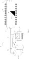
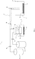
- the mist epitaxy device 19 includes a susceptor 21 having a substrate 20 placed thereon, carrier gas supply means 22a for supplying a carrier gas, a flow rate control valve 23a for controlling the flow rate of the carrier gas supplied from the carrier gas supply means 22a, carrier gas (dilution) supply means 22b for supplying a carrier gas (dilution), a flow rate control valve 23b for controlling the flow rate of the carrier gas (dilution) supplied from the dilution carrier gas supply means 22b, a mist source 24 containing a raw-material solution 24a, a container 25 containing water 25a, an ultrasonic transducer 26 mounted on the bottom of the container 25, a supply pipe 27 formed of a 40 mm-inner diameter quartz tube, a heater 28 disposed around the supply pipe 27, and an exhaust port 29 for exhausting a mist, droplets, and exhaust gas after thermal reaction.
- carrier gas supply means 22a for supplying a carrier gas
- a flow rate control valve 23a for controlling the flow rate of the carrier gas
- the susceptor 21 is formed of quartz, and the surface thereof for placing the substrate 20 is inclined from the horizontal plane. By forming both the supply pipe 27 serving as a film forming chamber and susceptor 21 from quartz, entry of device-derived impurities into a film formed on the substrate 20 is reduced.
- a solution prepared by dispersing rhodium acetylacetonate (0.01 mol/L) in a mixed solvent of methanol and water (methanol to water ratio 9.5:0.5) was used as a raw-material solution.
- C-plane sapphire was used as a substrate.
- Nitrogen was used as a carrier gas. The flow rate of the carrier gas was set to 5L/min, and the flow rate of the carrier gas (dilution) was set to 0.5L/min.
- a metal film was formed at 500°C in a nitrogen atmosphere.
- the formed metal film was confirmed to have a rhodium metal film formed therein.
- the thickness of the rhodium film was measured using a cross-sectional SEM image and found to be about 11.7 ⁇ m.
- the cross-sectional SEM image is shown in Fig. 2 .
- the surface of the metal film was observed using the SEM and found to be a less-bumpy, neat surface.
- a SEM image of this metal film surface is shown in Fig. 3 .
- Metal films were formed as in Example 1 except that the mixing ratio (volume ratio) between water and methanol was those shown in Table 1. The quality and adhesion of the formed metal films were evaluated. The results are shown in Table 1.
- Table 1 Volume ratio Film Formation Adhesion Water Methanol 0 100 ⁇ Film quality is not so good ⁇ Not so good 1 99 ⁇ Good ⁇ Good 5 95 ⁇ Good ⁇ Good 10 90 ⁇ Fairlv good ⁇ Good 20 80 ⁇ Fairly good ⁇ Fairly good 30 70 ⁇ Fairlv good ⁇ Fairly good 40 60 ⁇ Fairlv good ⁇ Fairlv good 50 50 ⁇ Colloid occurred (otherwise failv good) ⁇ Not so good 100 0 ⁇ Difficult to form film due, e.g., to coloring of substrate surface by yellow of raw material ⁇ Difficult to evaluate
- a metal film was formed as in Example 1 except that aluminum acetylacetonate was used in place of rhodium acetylacetonate. As a result, it was found that even when aluminum was used, a film could be formed in the same way as rhodium was used.
- the mist epitaxy device 1 includes a carrier gas source 2a for supplying a carrier gas, a flow rate control valve 3a for controlling the flow rate of the carrier gas supplied from the carrier gas source 2a, carrier gas (dilution) source 2b for supplying a carrier gas (dilution), a flow rate control valve 3b for controlling the flow rate of the carrier gas (dilution) supplied from the carrier gas (dilution) source 2b, a mist source 4 containing a raw-material solution 4a, a container 5 containing water 5a, an ultrasonic vibrator 6 mounted on the bottom of the container 5, a film forming chamber 7, a supply pipe 9 connecting the mist source 4a to the film forming chamber 7, a hot plate 8 mounted in the film forming chamber 7, and an exhaust port 11
- Copper acetylacetonate was mixed into methanol in such a manner that the concentration of copper acetylacetonate became 0.05 mol/L. Further, ethylenediamine was added as a chelating agent in such a manner that the concentration thereof in the mixed solution became 0.5 volume%. Thus, a raw-material solution 4a was prepared.
- the raw-material solution 4a obtained in the above 2. was charged into the mist source 4. Then, a glass substrate serving as the substrate 10 was placed on the hot plate 8, which was then operated to increase the temperature in the film forming chamber 7 to 500°C. Then, the flow rate control valves 3a, 3b were opened to supply carrier gases from the carrier-gas supply means 2a, 2b serving as carrier gas sources into the film forming chamber 7. After sufficiently substituting the carrier gases for the atmosphere in the film forming chamber 7, the flow rates of the carrier gas and the carrier gas (dilution) were adjusted to 5.0 L/min and 0.5 L/min, respectively. Nitrogen was used as the carrier gases.
- the ultrasonic transducer 6 was vibrated at 2.4 MHz in such a manner that the vibration propagated through the water 5a into the raw-material solution 4a.
- the raw-material solution 4a was atomized into a mist 4b.
- the mist 4b was introduced into the film forming chamber 7 by the carrier gas through the supply pipe 9.
- the mist then thermally reacted in the film forming chamber 7 under atmospheric pressure and at 400°C, so that a copper film was formed on the substrate 10.
- the film formation time was 30 min.
- the copper film was then checked using an X-ray measuring instrument.
- the XRD measurement results are shown in Fig. 5 .
- the thickness of the copper film was 200 nm. Further, the adhesion thereof was evaluated as in Example 1 and found to be good.
- a copper film was formed as in Example 4 except that the film formation temperature was set to 500°C in place of 400°C. The copper film was then checked using an X-ray measuring instrument. The XRD measurement results are shown in Fig. 6 . The thickness of the copper film was 925 nm. Further, the adhesion thereof was evaluated as in Example 1 and found to be good.
- Copper acetylacetonate was mixed into methanol in such a manner that the concentration of copper acetylacetonate became 0.05 mol/L. Further, hydrochloric acid was added as a protonic acid in such a manner that the concentration thereof in the mixed solution became 0.25 volume%. Thus, a raw-material solution was prepared. A copper film was formed as in Example 4 except that this raw-material solution was used in place of the raw-material solution 4a of Example 4. The copper film was then checked using an X-ray measuring instrument. The XRD measurement results are shown in Fig. 7 . The thickness of the copper film was 799 nm. Further, the adhesion thereof was evaluated as in Example 1 and found to be good.
- Example 4 In Examples 4, and 5, in which the chelating agent was used, the metal films had better luster.
- a surface image of the copper film formed in Example 5 is shown in Fig. 8 .
- Example 6 In Example 6, in which the protonic acid was used, the film formation rate was better.
- the metal film forming method of the present invention can be used in all fields, including semiconductors (e.g., compound semiconductor electronic devices), electronic components/electric apparatus components, optical/electronic image-related devices, and industrial materials.
- semiconductors e.g., compound semiconductor electronic devices
- electronic components/electric apparatus components e.g
Landscapes
- Chemical & Material Sciences (AREA)
- Engineering & Computer Science (AREA)
- Materials Engineering (AREA)
- Organic Chemistry (AREA)
- Metallurgy (AREA)
- Chemical Kinetics & Catalysis (AREA)
- General Chemical & Material Sciences (AREA)
- Mechanical Engineering (AREA)
- Microelectronics & Electronic Packaging (AREA)
- Power Engineering (AREA)
- Condensed Matter Physics & Semiconductors (AREA)
- Physics & Mathematics (AREA)
- General Physics & Mathematics (AREA)
- Crystallography & Structural Chemistry (AREA)
- Computer Hardware Design (AREA)
- Dispersion Chemistry (AREA)
- Ceramic Engineering (AREA)
- Life Sciences & Earth Sciences (AREA)
- Geochemistry & Mineralogy (AREA)
- Manufacturing & Machinery (AREA)
- Chemical Vapour Deposition (AREA)
- Chemically Coating (AREA)
- Electrodes Of Semiconductors (AREA)
Applications Claiming Priority (2)
| Application Number | Priority Date | Filing Date | Title |
|---|---|---|---|
| JP2014176648 | 2014-08-29 | ||
| JP2015108025A JP6945120B2 (ja) | 2014-08-29 | 2015-05-27 | 金属膜形成方法 |
Publications (2)
| Publication Number | Publication Date |
|---|---|
| EP2990503A1 EP2990503A1 (en) | 2016-03-02 |
| EP2990503B1 true EP2990503B1 (en) | 2022-01-12 |
Family
ID=54251921
Family Applications (1)
| Application Number | Title | Priority Date | Filing Date |
|---|---|---|---|
| EP15182652.6A Active EP2990503B1 (en) | 2014-08-29 | 2015-08-27 | Method of forming metal film |
Country Status (6)
| Country | Link |
|---|---|
| US (1) | US9828694B2 (ja) |
| EP (1) | EP2990503B1 (ja) |
| JP (1) | JP6945120B2 (ja) |
| KR (1) | KR101807544B1 (ja) |
| CN (2) | CN110952077B (ja) |
| TW (1) | TWI597381B (ja) |
Families Citing this family (18)
| Publication number | Priority date | Publication date | Assignee | Title |
|---|---|---|---|---|
| KR20210158882A (ko) * | 2016-03-11 | 2021-12-31 | 가부시키가이샤 니콘 | 미스트 발생장치, 성막장치, 미스트 발생 방법, 성막 방법, 및 디바이스 제조 방법 |
| CN107371338B (zh) * | 2016-05-13 | 2019-08-20 | 苏州卫鹏机电科技有限公司 | 一种超薄金属层的印刷线路板的制备方法 |
| KR20190022561A (ko) | 2016-06-30 | 2019-03-06 | 가부시키가이샤 플로스피아 | 산화물 반도체 막 및 그 제조 방법 |
| WO2018004009A1 (ja) | 2016-06-30 | 2018-01-04 | 株式会社Flosfia | p型酸化物半導体及びその製造方法 |
| JP6879483B2 (ja) * | 2016-07-30 | 2021-06-02 | 株式会社Flosfia | コンデンサの製造方法 |
| JP2018019052A (ja) * | 2016-07-30 | 2018-02-01 | 株式会社Flosfia | インダクタの製造方法 |
| JP2018019050A (ja) * | 2016-07-30 | 2018-02-01 | 株式会社Flosfia | 抵抗体の製造方法 |
| JP7064723B2 (ja) * | 2017-03-31 | 2022-05-11 | 株式会社Flosfia | 成膜方法 |
| CN109628910B (zh) | 2017-10-07 | 2023-06-30 | 株式会社Flosfia | 形成膜的方法 |
| JP2019119931A (ja) * | 2017-12-29 | 2019-07-22 | 株式会社Flosfia | 処理方法 |
| JP6875336B2 (ja) * | 2018-08-27 | 2021-05-26 | 信越化学工業株式会社 | 成膜方法 |
| JP7031564B2 (ja) * | 2018-11-14 | 2022-03-08 | トヨタ自動車株式会社 | 燃料電池用セパレータの製造方法 |
| JP2020092125A (ja) * | 2018-12-03 | 2020-06-11 | トヨタ自動車株式会社 | 成膜装置 |
| CN110318021B (zh) * | 2019-07-26 | 2020-08-25 | 中国科学技术大学 | 一种晶圆级二氧化钒薄膜的制备方法 |
| JP7261410B2 (ja) * | 2019-09-02 | 2023-04-20 | 信越化学工業株式会社 | 金属膜形成方法 |
| CN113439327B (zh) * | 2020-01-23 | 2023-07-25 | 株式会社日立高新技术 | 等离子体处理装置以及等离子体处理装置的工作方法 |
| CN111364020B (zh) * | 2020-04-10 | 2022-01-28 | 南昌航空大学 | 一种气溶胶传输辅助装置及输送方法 |
| CN112813406B (zh) * | 2020-12-30 | 2023-07-14 | 武汉工程大学 | 基于cvd技术在异形件表面制备三维金属单质薄膜的设备及方法 |
Family Cites Families (22)
| Publication number | Priority date | Publication date | Assignee | Title |
|---|---|---|---|---|
| US5034372A (en) * | 1987-12-07 | 1991-07-23 | Mitsubishi Denki Kabushiki Kaisha | Plasma based method for production of superconductive oxide layers |
| KR100479485B1 (ko) * | 1995-08-04 | 2005-09-07 | 마이크로코팅 테크놀로지, 인크. | 근초임계및초임계유동용액의열적분무를이용한화학증착및분말형성 |
| US6010969A (en) * | 1996-10-02 | 2000-01-04 | Micron Technology, Inc. | Method of depositing films on semiconductor devices by using carboxylate complexes |
| US6482374B1 (en) | 1999-06-16 | 2002-11-19 | Nanogram Corporation | Methods for producing lithium metal oxide particles |
| KR100460746B1 (ko) * | 1999-04-13 | 2004-12-09 | 주식회사 하이닉스반도체 | 반도체 소자의 구리 금속 배선 형성 방법 |
| JP3638487B2 (ja) | 1999-12-10 | 2005-04-13 | 株式会社荏原製作所 | 半導体素子の実装方法 |
| JP4781571B2 (ja) | 2001-07-31 | 2011-09-28 | エルピーダメモリ株式会社 | 半導体装置の製造方法 |
| AU2002337822A1 (en) * | 2001-10-05 | 2003-04-22 | Superior Micropowders Llc | Low viscosity precursor compositions and methods for the deposition of conductive electronic features |
| JP2004277585A (ja) * | 2003-03-17 | 2004-10-07 | Canon Inc | 有機顔料分散体製造方法および有機顔料分散体、水性着色液ならびにインクジェット記録用液 |
| DE102004001095A1 (de) * | 2004-01-05 | 2005-07-28 | Blue Membranes Gmbh | Hochfrequenzzerstäubungsvorrichtung |
| JP4841338B2 (ja) | 2005-07-14 | 2011-12-21 | 株式会社野田スクリーン | 成膜方法、および装置 |
| KR20080080154A (ko) * | 2005-12-29 | 2008-09-02 | 쓰리엠 이노베이티브 프로퍼티즈 컴파니 | 코팅 공정을 위한 물질의 분무화 방법 |
| EP2234119A4 (en) | 2007-12-18 | 2015-04-15 | Hitachi Chemical Co Ltd | COPPER CONDUCTIVE FILM AND MANUFACTURING METHOD THEREFOR, CONDUCTIVE SUBSTRATE AND METHOD FOR MANUFACTURING THE SAME, COPPER CONDUCTIVE THREAD AND METHOD FOR MANUFACTURING THE SAME, AND PROCESSING SOLUTION THEREOF |
| JP2009167522A (ja) | 2007-12-21 | 2009-07-30 | Shinko Electric Ind Co Ltd | 銅膜の形成方法 |
| KR100976264B1 (ko) | 2008-03-31 | 2010-08-18 | 주식회사 잉크테크 | 금속 박막 형성 장치 및 이를 이용한 금속 박막 형성 방법 |
| US20150004326A1 (en) * | 2008-05-07 | 2015-01-01 | Isaiah O. Oladeji | Apparatus and method for depositing alkali metals |
| US20110151619A1 (en) * | 2008-09-24 | 2011-06-23 | Toshiba Mitsubishi-Electric Industrial Sys. Corp. | Method of forming metal oxide film and apparatus for forming metal oxide film |
| JP5659495B2 (ja) | 2010-01-26 | 2015-01-28 | 三菱マテリアル株式会社 | 電極又は配線パターンの形成方法 |
| DE112010005624T5 (de) * | 2010-06-01 | 2013-03-21 | Kyoto University | Anlage zur Bildung eines Metalloxidfilmes, Verfahren zur Bildung eines Metalloxidfilmes und Metalloxidfilm |
| JP2013129887A (ja) | 2011-12-22 | 2013-07-04 | Nitto Denko Corp | 複合電極の形成方法 |
| JP5343224B1 (ja) | 2012-09-28 | 2013-11-13 | Roca株式会社 | 半導体装置および結晶 |
| MX2012011948A (es) | 2012-10-12 | 2014-04-24 | Vitro Vidrio Y Cristal S A De C V | Un recubrimiento con propiedades de control solar para un substrato y, un metodo y sistema para depositar dicho recubrimiento sobre el substrato. |
-
2015
- 2015-05-27 JP JP2015108025A patent/JP6945120B2/ja active Active
- 2015-08-27 EP EP15182652.6A patent/EP2990503B1/en active Active
- 2015-08-27 US US14/838,126 patent/US9828694B2/en active Active
- 2015-08-27 KR KR1020150121117A patent/KR101807544B1/ko active IP Right Grant
- 2015-08-27 TW TW104128055A patent/TWI597381B/zh active
- 2015-08-28 CN CN201911347903.6A patent/CN110952077B/zh active Active
- 2015-08-28 CN CN201510540239.2A patent/CN105386008B/zh active Active
Also Published As
| Publication number | Publication date |
|---|---|
| KR101807544B1 (ko) | 2017-12-11 |
| EP2990503A1 (en) | 2016-03-02 |
| CN105386008B (zh) | 2020-01-21 |
| CN110952077A (zh) | 2020-04-03 |
| TWI597381B (zh) | 2017-09-01 |
| US9828694B2 (en) | 2017-11-28 |
| KR20160026761A (ko) | 2016-03-09 |
| JP6945120B2 (ja) | 2021-10-06 |
| JP2016050357A (ja) | 2016-04-11 |
| TW201608048A (zh) | 2016-03-01 |
| CN110952077B (zh) | 2022-09-13 |
| US20160060788A1 (en) | 2016-03-03 |
| CN105386008A (zh) | 2016-03-09 |
Similar Documents
| Publication | Publication Date | Title |
|---|---|---|
| EP2990503B1 (en) | Method of forming metal film | |
| JP6478103B2 (ja) | 成膜装置および成膜方法 | |
| CN110870079B (zh) | 半导体装置 | |
| JP7014355B2 (ja) | 積層構造体および半導体装置 | |
| JP2016201540A (ja) | 結晶性酸化物半導体膜および半導体装置 | |
| JP2021009880A (ja) | エッチング処理方法およびエッチング処理装置 | |
| JP7240654B2 (ja) | 金属膜形成方法 | |
| JP7065440B2 (ja) | 半導体装置の製造方法および半導体装置 | |
| JP2023017874A (ja) | 酸化ガリウム膜及び積層体 | |
| TW202332813A (zh) | 積層體的製造方法、積層體的製造裝置、積層體以及半導體裝置 | |
| JP6999106B2 (ja) | 半導体装置 | |
| JP6999105B2 (ja) | 半導体装置の製造方法 | |
| JP6999103B2 (ja) | 半導体装置 | |
| JP2016079485A (ja) | 成膜方法ならびに膜形成用ミストおよびその前駆体溶液 | |
| JP7407426B2 (ja) | 半導体膜 | |
| JP7011207B2 (ja) | 成膜用ドーピング原料溶液の製造方法、積層体の製造方法、成膜用ドーピング原料溶液及び半導体膜 | |
| JP6999104B2 (ja) | 半導体装置 | |
| TWM639608U (zh) | 成膜裝置 | |
| JP6849874B2 (ja) | 積層構造体の製造方法 | |
| TW202242209A (zh) | 積層結構體、半導體裝置以及積層結構體的製造方法 | |
| JP2020047948A (ja) | 結晶性酸化物半導体膜、半導体装置 | |
| JP2018019050A (ja) | 抵抗体の製造方法 |
Legal Events
| Date | Code | Title | Description |
|---|---|---|---|
| PUAI | Public reference made under article 153(3) epc to a published international application that has entered the european phase |
Free format text: ORIGINAL CODE: 0009012 |
|
| 17P | Request for examination filed |
Effective date: 20150828 |
|
| AK | Designated contracting states |
Kind code of ref document: A1 Designated state(s): AL AT BE BG CH CY CZ DE DK EE ES FI FR GB GR HR HU IE IS IT LI LT LU LV MC MK MT NL NO PL PT RO RS SE SI SK SM TR |
|
| AX | Request for extension of the european patent |
Extension state: BA ME |
|
| STAA | Information on the status of an ep patent application or granted ep patent |
Free format text: STATUS: EXAMINATION IS IN PROGRESS |
|
| 17Q | First examination report despatched |
Effective date: 20180115 |
|
| RAP1 | Party data changed (applicant data changed or rights of an application transferred) |
Owner name: FLOSFIA INC. |
|
| STAA | Information on the status of an ep patent application or granted ep patent |
Free format text: STATUS: EXAMINATION IS IN PROGRESS |
|
| GRAP | Despatch of communication of intention to grant a patent |
Free format text: ORIGINAL CODE: EPIDOSNIGR1 |
|
| STAA | Information on the status of an ep patent application or granted ep patent |
Free format text: STATUS: GRANT OF PATENT IS INTENDED |
|
| INTG | Intention to grant announced |
Effective date: 20210910 |
|
| GRAS | Grant fee paid |
Free format text: ORIGINAL CODE: EPIDOSNIGR3 |
|
| GRAA | (expected) grant |
Free format text: ORIGINAL CODE: 0009210 |
|
| STAA | Information on the status of an ep patent application or granted ep patent |
Free format text: STATUS: THE PATENT HAS BEEN GRANTED |
|
| AK | Designated contracting states |
Kind code of ref document: B1 Designated state(s): AL AT BE BG CH CY CZ DE DK EE ES FI FR GB GR HR HU IE IS IT LI LT LU LV MC MK MT NL NO PL PT RO RS SE SI SK SM TR |
|
| REG | Reference to a national code |
Ref country code: GB Ref legal event code: FG4D |
|
| REG | Reference to a national code |
Ref country code: CH Ref legal event code: EP |
|
| REG | Reference to a national code |
Ref country code: DE Ref legal event code: R096 Ref document number: 602015076391 Country of ref document: DE |
|
| REG | Reference to a national code |
Ref country code: IE Ref legal event code: FG4D |
|
| REG | Reference to a national code |
Ref country code: AT Ref legal event code: REF Ref document number: 1462439 Country of ref document: AT Kind code of ref document: T Effective date: 20220215 |
|
| REG | Reference to a national code |
Ref country code: LT Ref legal event code: MG9D |
|
| REG | Reference to a national code |
Ref country code: NL Ref legal event code: MP Effective date: 20220112 |
|
| REG | Reference to a national code |
Ref country code: AT Ref legal event code: MK05 Ref document number: 1462439 Country of ref document: AT Kind code of ref document: T Effective date: 20220112 |
|
| PG25 | Lapsed in a contracting state [announced via postgrant information from national office to epo] |
Ref country code: NL Free format text: LAPSE BECAUSE OF FAILURE TO SUBMIT A TRANSLATION OF THE DESCRIPTION OR TO PAY THE FEE WITHIN THE PRESCRIBED TIME-LIMIT Effective date: 20220112 |
|
| PG25 | Lapsed in a contracting state [announced via postgrant information from national office to epo] |
Ref country code: SE Free format text: LAPSE BECAUSE OF FAILURE TO SUBMIT A TRANSLATION OF THE DESCRIPTION OR TO PAY THE FEE WITHIN THE PRESCRIBED TIME-LIMIT Effective date: 20220112 Ref country code: RS Free format text: LAPSE BECAUSE OF FAILURE TO SUBMIT A TRANSLATION OF THE DESCRIPTION OR TO PAY THE FEE WITHIN THE PRESCRIBED TIME-LIMIT Effective date: 20220112 Ref country code: PT Free format text: LAPSE BECAUSE OF FAILURE TO SUBMIT A TRANSLATION OF THE DESCRIPTION OR TO PAY THE FEE WITHIN THE PRESCRIBED TIME-LIMIT Effective date: 20220512 Ref country code: NO Free format text: LAPSE BECAUSE OF FAILURE TO SUBMIT A TRANSLATION OF THE DESCRIPTION OR TO PAY THE FEE WITHIN THE PRESCRIBED TIME-LIMIT Effective date: 20220412 Ref country code: LT Free format text: LAPSE BECAUSE OF FAILURE TO SUBMIT A TRANSLATION OF THE DESCRIPTION OR TO PAY THE FEE WITHIN THE PRESCRIBED TIME-LIMIT Effective date: 20220112 Ref country code: HR Free format text: LAPSE BECAUSE OF FAILURE TO SUBMIT A TRANSLATION OF THE DESCRIPTION OR TO PAY THE FEE WITHIN THE PRESCRIBED TIME-LIMIT Effective date: 20220112 Ref country code: ES Free format text: LAPSE BECAUSE OF FAILURE TO SUBMIT A TRANSLATION OF THE DESCRIPTION OR TO PAY THE FEE WITHIN THE PRESCRIBED TIME-LIMIT Effective date: 20220112 Ref country code: BG Free format text: LAPSE BECAUSE OF FAILURE TO SUBMIT A TRANSLATION OF THE DESCRIPTION OR TO PAY THE FEE WITHIN THE PRESCRIBED TIME-LIMIT Effective date: 20220412 |
|
| PG25 | Lapsed in a contracting state [announced via postgrant information from national office to epo] |
Ref country code: PL Free format text: LAPSE BECAUSE OF FAILURE TO SUBMIT A TRANSLATION OF THE DESCRIPTION OR TO PAY THE FEE WITHIN THE PRESCRIBED TIME-LIMIT Effective date: 20220112 Ref country code: LV Free format text: LAPSE BECAUSE OF FAILURE TO SUBMIT A TRANSLATION OF THE DESCRIPTION OR TO PAY THE FEE WITHIN THE PRESCRIBED TIME-LIMIT Effective date: 20220112 Ref country code: GR Free format text: LAPSE BECAUSE OF FAILURE TO SUBMIT A TRANSLATION OF THE DESCRIPTION OR TO PAY THE FEE WITHIN THE PRESCRIBED TIME-LIMIT Effective date: 20220413 Ref country code: FI Free format text: LAPSE BECAUSE OF FAILURE TO SUBMIT A TRANSLATION OF THE DESCRIPTION OR TO PAY THE FEE WITHIN THE PRESCRIBED TIME-LIMIT Effective date: 20220112 Ref country code: AT Free format text: LAPSE BECAUSE OF FAILURE TO SUBMIT A TRANSLATION OF THE DESCRIPTION OR TO PAY THE FEE WITHIN THE PRESCRIBED TIME-LIMIT Effective date: 20220112 |
|
| PG25 | Lapsed in a contracting state [announced via postgrant information from national office to epo] |
Ref country code: IS Free format text: LAPSE BECAUSE OF FAILURE TO SUBMIT A TRANSLATION OF THE DESCRIPTION OR TO PAY THE FEE WITHIN THE PRESCRIBED TIME-LIMIT Effective date: 20220512 |
|
| REG | Reference to a national code |
Ref country code: DE Ref legal event code: R097 Ref document number: 602015076391 Country of ref document: DE |
|
| PG25 | Lapsed in a contracting state [announced via postgrant information from national office to epo] |
Ref country code: SM Free format text: LAPSE BECAUSE OF FAILURE TO SUBMIT A TRANSLATION OF THE DESCRIPTION OR TO PAY THE FEE WITHIN THE PRESCRIBED TIME-LIMIT Effective date: 20220112 Ref country code: SK Free format text: LAPSE BECAUSE OF FAILURE TO SUBMIT A TRANSLATION OF THE DESCRIPTION OR TO PAY THE FEE WITHIN THE PRESCRIBED TIME-LIMIT Effective date: 20220112 Ref country code: RO Free format text: LAPSE BECAUSE OF FAILURE TO SUBMIT A TRANSLATION OF THE DESCRIPTION OR TO PAY THE FEE WITHIN THE PRESCRIBED TIME-LIMIT Effective date: 20220112 Ref country code: EE Free format text: LAPSE BECAUSE OF FAILURE TO SUBMIT A TRANSLATION OF THE DESCRIPTION OR TO PAY THE FEE WITHIN THE PRESCRIBED TIME-LIMIT Effective date: 20220112 Ref country code: DK Free format text: LAPSE BECAUSE OF FAILURE TO SUBMIT A TRANSLATION OF THE DESCRIPTION OR TO PAY THE FEE WITHIN THE PRESCRIBED TIME-LIMIT Effective date: 20220112 Ref country code: CZ Free format text: LAPSE BECAUSE OF FAILURE TO SUBMIT A TRANSLATION OF THE DESCRIPTION OR TO PAY THE FEE WITHIN THE PRESCRIBED TIME-LIMIT Effective date: 20220112 |
|
| PLBE | No opposition filed within time limit |
Free format text: ORIGINAL CODE: 0009261 |
|
| STAA | Information on the status of an ep patent application or granted ep patent |
Free format text: STATUS: NO OPPOSITION FILED WITHIN TIME LIMIT |
|
| PG25 | Lapsed in a contracting state [announced via postgrant information from national office to epo] |
Ref country code: AL Free format text: LAPSE BECAUSE OF FAILURE TO SUBMIT A TRANSLATION OF THE DESCRIPTION OR TO PAY THE FEE WITHIN THE PRESCRIBED TIME-LIMIT Effective date: 20220112 |
|
| 26N | No opposition filed |
Effective date: 20221013 |
|
| PG25 | Lapsed in a contracting state [announced via postgrant information from national office to epo] |
Ref country code: SI Free format text: LAPSE BECAUSE OF FAILURE TO SUBMIT A TRANSLATION OF THE DESCRIPTION OR TO PAY THE FEE WITHIN THE PRESCRIBED TIME-LIMIT Effective date: 20220112 |
|
| PG25 | Lapsed in a contracting state [announced via postgrant information from national office to epo] |
Ref country code: MC Free format text: LAPSE BECAUSE OF FAILURE TO SUBMIT A TRANSLATION OF THE DESCRIPTION OR TO PAY THE FEE WITHIN THE PRESCRIBED TIME-LIMIT Effective date: 20220112 |
|
| REG | Reference to a national code |
Ref country code: CH Ref legal event code: PL |
|
| PG25 | Lapsed in a contracting state [announced via postgrant information from national office to epo] |
Ref country code: LU Free format text: LAPSE BECAUSE OF NON-PAYMENT OF DUE FEES Effective date: 20220827 Ref country code: LI Free format text: LAPSE BECAUSE OF NON-PAYMENT OF DUE FEES Effective date: 20220831 Ref country code: CH Free format text: LAPSE BECAUSE OF NON-PAYMENT OF DUE FEES Effective date: 20220831 |
|
| REG | Reference to a national code |
Ref country code: BE Ref legal event code: MM Effective date: 20220831 |
|
| PG25 | Lapsed in a contracting state [announced via postgrant information from national office to epo] |
Ref country code: IT Free format text: LAPSE BECAUSE OF FAILURE TO SUBMIT A TRANSLATION OF THE DESCRIPTION OR TO PAY THE FEE WITHIN THE PRESCRIBED TIME-LIMIT Effective date: 20220112 Ref country code: IE Free format text: LAPSE BECAUSE OF NON-PAYMENT OF DUE FEES Effective date: 20220827 |
|
| PG25 | Lapsed in a contracting state [announced via postgrant information from national office to epo] |
Ref country code: BE Free format text: LAPSE BECAUSE OF NON-PAYMENT OF DUE FEES Effective date: 20220831 |
|
| PGFP | Annual fee paid to national office [announced via postgrant information from national office to epo] |
Ref country code: GB Payment date: 20230706 Year of fee payment: 9 |
|
| PGFP | Annual fee paid to national office [announced via postgrant information from national office to epo] |
Ref country code: FR Payment date: 20230703 Year of fee payment: 9 Ref country code: DE Payment date: 20230703 Year of fee payment: 9 |
|
| PG25 | Lapsed in a contracting state [announced via postgrant information from national office to epo] |
Ref country code: HU Free format text: LAPSE BECAUSE OF FAILURE TO SUBMIT A TRANSLATION OF THE DESCRIPTION OR TO PAY THE FEE WITHIN THE PRESCRIBED TIME-LIMIT; INVALID AB INITIO Effective date: 20150827 |
|
| PG25 | Lapsed in a contracting state [announced via postgrant information from national office to epo] |
Ref country code: CY Free format text: LAPSE BECAUSE OF FAILURE TO SUBMIT A TRANSLATION OF THE DESCRIPTION OR TO PAY THE FEE WITHIN THE PRESCRIBED TIME-LIMIT Effective date: 20220112 |