EP2943049B1 - Elektronische vorrichtung - Google Patents
Elektronische vorrichtung Download PDFInfo
- Publication number
- EP2943049B1 EP2943049B1 EP14868704.9A EP14868704A EP2943049B1 EP 2943049 B1 EP2943049 B1 EP 2943049B1 EP 14868704 A EP14868704 A EP 14868704A EP 2943049 B1 EP2943049 B1 EP 2943049B1
- Authority
- EP
- European Patent Office
- Prior art keywords
- metal member
- electronic component
- electronic device
- enclosing
- slot
- Prior art date
- Legal status (The legal status is an assumption and is not a legal conclusion. Google has not performed a legal analysis and makes no representation as to the accuracy of the status listed.)
- Active
Links
Images

Classifications
-
- H—ELECTRICITY
- H05—ELECTRIC TECHNIQUES NOT OTHERWISE PROVIDED FOR
- H05K—PRINTED CIRCUITS; CASINGS OR CONSTRUCTIONAL DETAILS OF ELECTRIC APPARATUS; MANUFACTURE OF ASSEMBLAGES OF ELECTRICAL COMPONENTS
- H05K9/00—Screening of apparatus or components against electric or magnetic fields
- H05K9/0007—Casings
- H05K9/0049—Casings being metallic containers
-
- H—ELECTRICITY
- H05—ELECTRIC TECHNIQUES NOT OTHERWISE PROVIDED FOR
- H05K—PRINTED CIRCUITS; CASINGS OR CONSTRUCTIONAL DETAILS OF ELECTRIC APPARATUS; MANUFACTURE OF ASSEMBLAGES OF ELECTRICAL COMPONENTS
- H05K9/00—Screening of apparatus or components against electric or magnetic fields
- H05K9/0073—Shielding materials
- H05K9/0081—Electromagnetic shielding materials, e.g. EMI, RFI shielding
-
- B—PERFORMING OPERATIONS; TRANSPORTING
- B29—WORKING OF PLASTICS; WORKING OF SUBSTANCES IN A PLASTIC STATE IN GENERAL
- B29C—SHAPING OR JOINING OF PLASTICS; SHAPING OF MATERIAL IN A PLASTIC STATE, NOT OTHERWISE PROVIDED FOR; AFTER-TREATMENT OF THE SHAPED PRODUCTS, e.g. REPAIRING
- B29C45/00—Injection moulding, i.e. forcing the required volume of moulding material through a nozzle into a closed mould; Apparatus therefor
- B29C45/14—Injection moulding, i.e. forcing the required volume of moulding material through a nozzle into a closed mould; Apparatus therefor incorporating preformed parts or layers, e.g. injection moulding around inserts or for coating articles
- B29C45/14639—Injection moulding, i.e. forcing the required volume of moulding material through a nozzle into a closed mould; Apparatus therefor incorporating preformed parts or layers, e.g. injection moulding around inserts or for coating articles for obtaining an insulating effect, e.g. for electrical components
-
- G—PHYSICS
- G06—COMPUTING OR CALCULATING; COUNTING
- G06F—ELECTRIC DIGITAL DATA PROCESSING
- G06F1/00—Details not covered by groups G06F3/00 - G06F13/00 and G06F21/00
- G06F1/16—Constructional details or arrangements
- G06F1/1613—Constructional details or arrangements for portable computers
- G06F1/1633—Constructional details or arrangements of portable computers not specific to the type of enclosures covered by groups G06F1/1615 - G06F1/1626
- G06F1/1656—Details related to functional adaptations of the enclosure, e.g. to provide protection against EMI, shock, water, or to host detachable peripherals like a mouse or removable expansions units like PCMCIA cards, or to provide access to internal components for maintenance or to removable storage supports like CDs or DVDs, or to mechanically mount accessories
-
- G—PHYSICS
- G06—COMPUTING OR CALCULATING; COUNTING
- G06F—ELECTRIC DIGITAL DATA PROCESSING
- G06F1/00—Details not covered by groups G06F3/00 - G06F13/00 and G06F21/00
- G06F1/16—Constructional details or arrangements
- G06F1/18—Packaging or power distribution
- G06F1/181—Enclosures
- G06F1/182—Enclosures with special features, e.g. for use in industrial environments; grounding or shielding against radio frequency interference [RFI] or electromagnetical interference [EMI]
-
- H—ELECTRICITY
- H05—ELECTRIC TECHNIQUES NOT OTHERWISE PROVIDED FOR
- H05K—PRINTED CIRCUITS; CASINGS OR CONSTRUCTIONAL DETAILS OF ELECTRIC APPARATUS; MANUFACTURE OF ASSEMBLAGES OF ELECTRICAL COMPONENTS
- H05K9/00—Screening of apparatus or components against electric or magnetic fields
- H05K9/0007—Casings
- H05K9/002—Casings with localised screening
- H05K9/0022—Casings with localised screening of components mounted on printed circuit boards [PCB]
-
- B—PERFORMING OPERATIONS; TRANSPORTING
- B29—WORKING OF PLASTICS; WORKING OF SUBSTANCES IN A PLASTIC STATE IN GENERAL
- B29K—INDEXING SCHEME ASSOCIATED WITH SUBCLASSES B29B, B29C OR B29D, RELATING TO MOULDING MATERIALS OR TO MATERIALS FOR MOULDS, REINFORCEMENTS, FILLERS OR PREFORMED PARTS, e.g. INSERTS
- B29K2995/00—Properties of moulding materials, reinforcements, fillers, preformed parts or moulds
- B29K2995/0003—Properties of moulding materials, reinforcements, fillers, preformed parts or moulds having particular electrical or magnetic properties, e.g. piezoelectric
- B29K2995/0005—Conductive
-
- B—PERFORMING OPERATIONS; TRANSPORTING
- B29—WORKING OF PLASTICS; WORKING OF SUBSTANCES IN A PLASTIC STATE IN GENERAL
- B29L—INDEXING SCHEME ASSOCIATED WITH SUBCLASS B29C, RELATING TO PARTICULAR ARTICLES
- B29L2031/00—Other particular articles
- B29L2031/34—Electrical apparatus, e.g. sparking plugs or parts thereof
- B29L2031/3481—Housings or casings incorporating or embedding electric or electronic elements
Definitions
- the present invention relates to the field of electronic technologies, and in particular, to an electronic device.
- An electronic device generally includes a circuit board on which an electronic component is disposed and a diecasting metal member on which a hole or slot is disposed, where the diecasting metal member is also used as shielding space of the electronic component.
- a purpose of disposing the hole or slot is to reduce a weight of the diecasting metal member, or the hole or slot needs to be disposed because of a spatial constraint of a product structure and because of a component layout (for example: a component is high, and in order not to increase an overall thickness, a hole or slot needs to be disposed on some part of the diecasting metal member).
- the diecasting metal member may be made into different complex shapes and structures according to a need.
- the hole or slot is disposed on the metal member, and an electromagnetic wave of the electronic component can pass through the hole or slot, affecting operation of an electronic component on the other side of the diecasting metal member.
- an electromagnetic wave generated by the electronic component is prevented, in a manner of sticking an electrically conductive film, from passing through the hole or slot.
- US 7518880 B1 discloses a shielding arrangement for an electronic component mounted on a circuit board which includes a shield formed by a frame sidewall arranged to be oriented upstanding from the circuit board and surrounding the electronic component mounted on the circuit board.
- a first cover portion substantially closes the surrounding sidewall, enclosing the electronic component on the circuit board.
- a conductive layer, formed by vacuum deposition covers an inside surface of the surrounding sidewall and an inside surface of the first cover portion, continuously.
- the frame can be composed of an electrically conductive plastic.
- the first cover portion can be a stamped metal plate integrated with the frame by overmolding.
- Embodiments of the present invention provide an electronic device, resolving a technical problem in the prior art that, because a thickness a diecasting metal member itself is relatively large, sticking an electrically conductive film on a hole or slot of the diecasting metal member increases a thickness of an electronic device.
- a first aspect of an embodiment of the present invention provides an electronic device, where the electronic device includes: a metal member, a circuit board, and a shielding member, where a through hole or slot is disposed on the metal member, and the metal member is a stamped metal member or a forged metal member; an electronic component is disposed on the circuit board; the shielding member includes a blocking portion and an enclosing portion, the blocking portion is made of an electrically conductive plastic material, and the enclosing portion is made of a metal material or an electrically conductive plastic material; the blocking portion is configured to block the through hole or slot, the enclosing portion is disposed around the electronic component, one end of the enclosing portion is electrically connected to the metal member, and the other end of the enclosing portion is electrically connected to ground copper of the circuit board; the metal member, the blocking portion, the enclosing portion, and the circuit board form shielding space, and the electronic component is located in the shielding space.
- the shielding member further includes a buckling portion connected to the blocking portion, and the buckling portion is buckled in the through hole or slot.
- the shielding member further includes a fastening portion connected to the buckling portion, and a size of the fastening portion is greater than a size of the through hole or slot.
- An electrically conductive elastic member is disposed between the enclosing portion and the circuit board or between the enclosing portion and the metal member.
- the electronic device further includes a reinforcing portion that is configured to enhance strength of the metal member and is fastened on the metal member.
- the reinforcing portion is disposed opposite to the electronic component.
- the through hole or slot is disposed opposite to the electronic component.
- the electrically conductive plastic material is specifically electrically and thermally conductive plastic.
- an insulation layer is disposed on a surface, away from the metal member, of the blocking portion.
- the blocking portion and the enclosing portion are integrally injection molded, or the blocking portion, the enclosing portion, and the metal member are integrally metal injection molded.
- the blocking portion configured to block the through hole or slot on the metal member and the enclosing portion disposed around the electronic component are disposed, where one end of the enclosing portion is electrically connected to the metal member, and the other end of the enclosing portion is electrically connected to the ground copper of the circuit board.
- the ground copper is disposed on the circuit board, and the enclosing portion is made of an electrically conductive material, and therefore, enclosed space in which the electronic component is disposed is formed by the metal member, the circuit board, the blocking portion, and the enclosing portion, and an electromagnetic wave generated on the metal member is transferred to the ground copper of the circuit board by the enclosing portion, to be conducted away, so that shielding space enclosing the electronic component is formed, so as to reduce or prevent outward radiation of an electromagnetic wave generated by the electronic component, thereby preventing operation of another electronic component from being affected.
- the metal member is a stamped metal member or a forged metal member
- a thickness of the stamped metal member or a thickness of the forged metal member is less than a thickness of the diecasting metal member, and therefore, even after the shielding member is formed on the metal member, a sum of a thickness of the metal member and a thickness of the shielding member is also less than a sum of the thickness of the diecasting metal member and a thickness of an electrically conductive film. Therefore, the foregoing electronic device resolves a technical problem in the prior art that, because the thickness of the diecasting metal member itself is relatively large, sticking the electrically conductive film on the hole or slot of the diecasting metal member increases a thickness of the electronic device.
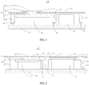
- FIG. 1 is a schematic structural diagram of an electronic device 100 according to an implementation manner of the present invention.
- the electronic device may be a device such as a mobile phone, a PAD, a computer, a television, or a server.
- the electronic device 100 includes a metal member 10, a circuit board 20, and a shielding member 30.
- a through hole or slot 11 is disposed on the metal member 10, a shape and a size of the hole or slot 11 may be set according to a need.
- a function of disposing the through hole or slot 11 is mainly to reduce a weight of metal of the electronic device 100, or is for stress relief, or is to make way for an electronic component in the electronic device 100, or is to fasten an element that needs to be fastened on the metal member 10. Therefore, according to a need, a quantity of through holes or slots 11 may be one, or may be multiple. As shown in FIG. 1 , the quantity of through holes or slots 11 is one, and disposing the through hole or slot 11 is to reduce a weight of the electronic device 100.
- a purpose of disposing the through hole or slot 11 may be to make way for the electronic component.
- the quantity of through holes or slots 11 is three, where some of the through holes or slots 11 are for reducing the weight of the electronic device 100, and a purpose of disposing other two through holes or slots 11 is to fasten the element that needs to be fastened on the metal member 10.
- the element may be the shielding member 30.
- the quantity of through holes or slots 11 is two, and a purpose of disposing the two through holes or slots 11 is to fasten the element that needs to be fastened on the metal member 10.
- the element may be the shielding member 30.
- the metal member 10 may be a stamped metal member or a forged metal member.
- the stamped metal member has a fine heat-conducting feature (a thermal conductivity coefficient may be greater than 250W/m-K), a low manufacturing cost, and a small wall thickness (in a case in which there is no strength requirement, the wall thickness may be ⁇ 0.1mm).
- weldability of the stamped metal member is better than that of a diecasting metal member, but a complex shielding cavity cannot be made in the stamped metal member and local thickening cannot be performed on the stamped metal member, and only a mechanical part with a simple structure requirement and a uniform wall thickness can be made (local thinning may be performed by means of an etching process, but in consideration of a process and a cost, a thickness difference is generally within 0.2mm).
- a heat-conducting feature of the diecasting metal member is worse than that of a stamped member, but a complex shielding cavity can be made and local thickening can be performed, resulting in high structural strength of the diecasting metal member.
- a CNC full name: computer numerical control machine, Computer numerical control machine
- a wall thickness of the diecasting metal member is greater than that of the stamped metal member (the wall thickness: mostly ⁇ 0.4mm, and locally ⁇ 0.3mm), and welding the diecasting metal member is difficult.
- performance of the forged metal member is between that of the diecasting metal member and that of the stamped metal member.
- the circuit board 20 may include an electronic component 21 and an electronic component 22.
- a height of the electronic component 22 is greater than a height of the electronic component 21.
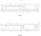
- the electronic component 21 and the electronic component 22 may be disposed opposite to the through hole or slot 11, or may not be disposed opposite to the through hole or slot 11. As shown in FIG. 1 , the electronic component 21 is disposed opposite to one through hole or slot 11, but the electronic component 22 is not disposed opposite to the through hole or slot 11. In FIG. 3 and FIG. 4 , neither the electronic component 21 nor the electronic component 22 is disposed opposite to the through hole or slot 11.
- the size of the hole or slot 11 may be set according to a need, that is, the size of the electronic component 21 may be greater than the size of the hole or slot 11, or may be smaller than the size of the hole or slot 11.
- the size of the hole or slot 11 may be greater than that of the electronic component 21, and a part of the electronic component 21 is disposed in the hole or slot 11, so as to reduce a distance between the metal member 10 and the circuit board 20, thereby reducing an overall thickness of the electronic device 100.
- the shielding member 30 is fastened on the metal member 10, and is configured to shield an electromagnetic wave generated by the electronic component 21.
- the shielding member 30 includes a blocking portion 31 and an enclosing portion 33.
- the shielding member 30 may be formed by one portion, may be formed by connecting two separate portions such as the blocking portion 31 and the enclosing portion 33, or may be formed by using a connecting portion to connect the blocking portion 31 and the enclosing portion 33; or the blocking portion 31 and the enclosing portion 33 may be two independent and separated portions.
- the blocking portion 31 is made of an electrically conductive plastic material
- the enclosing portion 33 is made of a metal material or an electrically conductive plastic material
- the blocking portion 31 and the enclosing portion 33 may be integrally injection molded
- the blocking portion 31, the enclosing portion 33, and the metal member 10 may be integrally metal injection molded.
- the blocking portion 31 may be made of the electrically conductive plastic material, the blocking portion 31 is configured to block the through hole or slot 11, to reduce or prevent passing, by the electromagnetic wave generated by the electronic component 21, through the through hole or slot 11.
- a quantity of blocking portions 31 is determined according to the quantity of through holes or slots 11, and when the quantity of blocking portions 31 is two or more than two, whether the blocking portions 31 are connected may be set according to a need. As shown in FIG. 1 , the quantity of through holes or slots 11 is one, and therefore, the quantity of blocking portions 31 may be one; in FIG. 2 and FIG.
- the quantity of through holes or slots 11 is three, and therefore, the quantity of blocking portions 31 is three, where one of the three blocking portions 31 is separate and is not connected to the other two blocking portions 31, and because strength of a metal member 10 between the other two blocking portions 31 needs to be enhanced or space is sufficient, a connecting portion or a reinforcing portion 37 configured to connect the two blocking portions 31 is disposed between the other two blocking portions 31.
- One or more reinforcing portions 37 may be disposed according to a need, the reinforcing portion 37 may be independent, or may be integrally formed with the blocking portion 31.
- a thickness of each part of each reinforcing portion 37 may be different.
- a material of the reinforcing portion 37 is the same as a material of the blocking portion 31, and in another implementation manner, the reinforcing portion 37 may be made of a plastic insulation material.
- the quantity of through holes or slots 11 is two, and therefore, the quantity of blocking portions 31 is two, and the two blocking portions 31 are independent, that is, the two blocking portions 31 are not connected to each other, or the two blocking portions 31 may be connected as a whole in another part according to a structural design requirement.
- Strength of a part that is of the metal member 10 and opposite to the electronic component 21 needs to be enhanced, and therefore, an reinforcing portion 37 connected to one of the two blocking portions 31 is disposed on a surface that is of the metal member 10 and opposite to the electronic component 21.
- the reinforcing portion 37 is connected to one blocking portion 31, and in another implementation manner, the reinforcing portion 37 may be independent and may not be connected to the blocking portion 31 or the enclosing portion 33.
- the quantity of through holes or slots 11 is two, and therefore, the quantity of blocking portions 31 is two, and the two blocking portions 31 are independent, that is, the two blocking portions 31 are not connected to each other, a connection part may be disposed, according to a structural design requirement, on a location allowed by a product thickness, such as an edge, and a location where a relatively short component is.
- the blocking portion 31, when there is sufficient space in the electronic device 100, the blocking portion 31, after being injection molded, may be fastened on the metal member 10 in a bonding manner or in a screw locking manner.
- the blocking portion 31 When there is limited space in the electronic device 100, the blocking portion 31 may be directly injection molded on the metal member 10, in this way, a thickness of the blocking portion 31 may be made relatively small, so as to reduce the thickness of the electronic device 100.
- the blocking portion 31 may be formed on the metal member 10 in a metal injection molding manner.
- the electrically conductive plastic material may be specifically electrically and thermally conductive plastic, which has a desirable heat-conducting property, and therefore, when the blocking portion 31 is an electrically conductive plastic material, the blocking portion 31 may be in direct contact with the electronic component 21.
- a thermal interface material such as a thermally conductive pad may be added between the electronic component 21 and the blocking portion 31, thereby achieving a smaller heat transfer thermal resistance, and increasing the heat conduction efficiency between the blocking portion 31 and the electronic component 21.
- an insulation layer is set on a surface, away from the metal member 10, of the blocking portion 31. By setting the insulation layer, after the blocking portion 31 is deformed, the electromagnetic wave generated by the electronic component 21 can still be shielded.
- a structure for example, this structure may be an insulation layer
- this structure may be an insulation layer covering the electronic component 21 may be formed on the metal member 10 in an injection molding manner and the like, to prevent the electromagnetic wave generated by the electronic component 21 from passing through the hole or slot 11 on the metal member 10.
- the enclosing portion 33 is made of a metal material or an electrically conductive plastic material, the enclosing portion 33 is disposed around the electronic component 21, one end of the enclosing portion 33 is in contact with the metal member 10 through an electrically conductive elastic member 40, and the other end of the enclosing portion 33 is in contact with the circuit board 20. Specifically, the other end of the enclosing portion 33 is electrically connected to ground copper of the circuit board 20.
- the ground copper is disposed on the circuit board 20 and the enclosing portion 33 is made of an electrically conductive material, and therefore, a charge generated on the metal member 10 may be transferred to the ground copper of the circuit board 20 by using the enclosing portion 33, to be conducted away, thereby reducing or preventing radiation and interference caused by the electromagnetic wave generated by the electronic component 21 to surroundings.
- the enclosing portion 33 comes into contact with the metal member 10 by using the electrically conductive elastic member 40, and in another implementation manner, the enclosing portion 33 may be in direct contact with the metal member 10.
- a quantity of enclosing portions 33 may be set according to a quantity of electronic components. As shown in FIG. 1, FIG. 2 , FIG. 5, and FIG. 6 , both the electronic component 21 and the electronic component 22 need to be shielded, and therefore, two shielding cavities are formed, where one shields the electronic component 21, and the other shields the electronic component 22.
- the enclosing portion 33 disposed around the electronic component 21 is made of a metal material
- the enclosing portion 33 disposed around the electronic component 22 is made of an electrically conductive plastic material, and the enclosing portion 33 is a separate element
- the enclosing portion 33 may be fastened on the circuit board 20 by means of welding
- the enclosing portion 33 is made of an electrically conductive material
- the enclosing portion 33 may be fastened on the circuit board 20 by using a fastening member such as a screw.
- both the enclosing portion 33 disposed around the electronic component 21 and the enclosing portion 33 disposed around the electronic component 22 are made of the metal material.
- the enclosing portion 33 when the enclosing portion 33 is made of the electrically conductive plastic material, the enclosing portion 33 may be a separate element, or may be integrally formed with the blocking portion 31 and formed on the metal member 10 in an injection molding manner.
- the enclosing portion 33 may be set as a separate metal member, and as shown in FIG. 5 , the enclosing portion 33 disposed around the electronic component 21 is a separate metal member. As shown in FIG. 6 , the enclosing portion 33 disposed around the electronic component 21 and the enclosing portion 33 disposed around the electronic component 22 are both separate metal members.
- the electronic component 21 is in shielding space, so as to prevent the electromagnetic wave generated by the electronic component 21 from affecting another electronic component.
- the electromagnetic wave generated by the electronic component 21 can be shielded by the blocking portion 31, the enclosing portion 33, and the metal member 10, so as to reduce or prevent outward radiation of the electromagnetic wave generated by the electronic component 21, thereby preventing operation of the another electronic component from being affected.
- the metal member 10, the enclosing portion 33, and the circuit board form shielding space, so that the electronic component 22 is in the shielding space, as shown in FIG. 1 .
- a thermally conductive material with a thermal conductivity coefficient k greater than 1W/m-K may be selected and used as the electrically conductive plastic material.
- the blocking portion 31 configured to block the through hole or slot 11 on the metal member 10 and the enclosing portion 33 disposed around the electronic component 21 are disposed, where one end of the enclosing portion 33 is electrically connected to the metal member 10, and the other end of the enclosing portion 33 is electrically connected to the circuit board 20.
- the ground copper is disposed on the circuit board 20, and the enclosing portion 33 is made of an electrically conductive material, and therefore, enclosed space in which the electronic component 21 is located is formed among the metal member 10, the circuit board 20, the blocking portion 31, and the enclosing portion 33, and an electromagnetic wave generated on the metal member 10 is transferred to the ground copper of the circuit board 20 by the enclosing portion 33, to be conducted away, so that shielding space enclosing the electronic component 21 is formed, so as to reduce or prevent outward radiation of the electromagnetic wave generated by the electronic component 21, thereby preventing operation of another electronic component from being affected.
- the metal member 10 may be a stamped metal member or a forged metal member, a thickness of the stamped metal member or a thickness of the forged metal member is less than a thickness of the diecasting metal member, and therefore, even after the shielding member 30 is formed on the metal member 10, a sum of a thickness of the metal member 10 and a thickness of the shielding member 30 is also less than a sum of the thickness of the diecasting metal member and a thickness of an electrically conductive film.
- the foregoing electronic device 100 resolves a technical problem in the prior art that, because the thickness of the diecasting metal member itself is relatively large, sticking the electrically conductive film on the hole or slot of the diecasting metal member further increases a thickness of the electronic device.
- combination of the stamped metal member or the forged metal member and the electrically conducive plastic member compared with original combination of the forged metal member and common plastic, not only enhances mechanical reliability of the metal member and the plastic member, and a cost of using an electrically and thermally conductive plastic member, compared with a cost of using common insulation plastic that is thermally conductive, is also reduced.
- an electrically conductive shielding cavity or isolation cavity may be made, that is, the blocking portion 31 and the enclosing portion 33 may be formed on the metal member 10 in a one-off manner.
- a thickness of each part of the shielding member 30 may be different from a thickness of the metal member 10, and when strength of a part of the metal member 10 needs to be enhanced, electrically conductive plastic needs to be injection molded on this part of the metal member 10, and a thickness of the electrically conductive plastic may be set according to a need; when space in a thickness direction of the electronic device 100 is limited, plastic may not be injection molded on a part whose thickness is limited and that is of the metal member 10, so that an overall thickness of a product is not increased.
- the shielding member 30 when the blocking portion 31 is located between the electronic component 21 and the metal member 10, to increase a structural binding force between the blocking portion 31 and the metal member 10, the shielding member 30 includes a buckling portion 32 connected to the blocking portion 31, and the buckling portion 32 is buckled in the through hole or slot 11, thereby increasing the structural binding force between the blocking portion 31 and the metal member 10, increasing stability of the blocking portion 31, and reducing a possibility that the blocking portion 31 is separated from the metal member 10.
- the blocking portion 31 and the buckling portion 32 may be integrally formed, and certainly, may also be two elements, where the blocking portion 31 and the buckling portion 32 are combined in a bonding manner.
- the shielding member 30 further includes a fastening portion 34 connected to the buckling portion 32, where the fastening portion 34 and the blocking portion 31 are separately disposed on two opposite sides of the metal member 10, and a size of the fastening portion 34 is greater than the size of the through hole or slot 11.
- the blocking portion 31, the buckling portion 32, and the fastening portion 34 may be integrally formed, and certainly, the blocking portion 31, the buckling portion 32, and the fastening portion 34 may also be combined in a bonding manner.
- the fastening portion 34 whose size is greater than that of the through hole or slot 11 on another side of the metal member 10, thereby preventing the shielding member 30 from departing from the metal member 10, and increasing stability of the shielding member 30.
- the electrically conductive elastic member 40 is disposed between the enclosing portion 33 and the circuit board 20.
- the electrically conductive elastic member 40 may be an electrically conductive elastomer or electrically conductive foam.
- the enclosing portion 33 may not be in direct contact with the ground copper of the circuit board 20, but may come into contact with the ground copper by using the electrically conductive elastic member 40.
- the ground copper of the circuit board 20 may be a copper layer on a surface layer of the circuit board 20.
- the blocking portion 31 configured to block the through hole or slot 11 on the metal member 10 and the enclosing portion 33 disposed around the electronic component 21 are disposed, where one end of the enclosing portion 33 is electrically connected to the metal member 10, and the other end of the enclosing portion 33 is electrically connected to the ground copper of the circuit board 20.
- the ground copper is disposed on the circuit board 20 and the enclosing portion 33 is made of an electrically conductive material, and therefore, enclosed space in which the electronic component 21 is located is formed among the metal member 10, the circuit board 20, the blocking portion 31, and the enclosing portion 33, and an electromagnetic wave generated on the metal member 10 is transferred to the ground copper of the circuit board 20 by the enclosing portion 33, to be conducted away, so that shielding space enclosing the electronic component 21 is formed, so as to reduce or prevent outward radiation of the electromagnetic wave generated by the electronic component 21, thereby preventing operation of another electronic component from being affected.
- the metal member 10 may be a stamped metal member or a forged metal member, a thickness of the stamped metal member or a thickness of the forged metal member is less than a thickness of the diecasting metal member, and therefore, even after the shielding member 30 is formed on the metal member 10, a sum of a thickness of the metal member 10 and a thickness of the shielding member 30 is also less than a sum of the thickness of the diecasting metal member and a thickness of an electrically conductive film.
- the foregoing electronic device 100 resolves a technical problem in the prior art that, because the thickness of the diecasting metal member itself is relatively large, sticking the electrically conductive film on the hole or slot of the diecasting metal member further increases a thickness of the electronic device.
- the buckling portion 32 connected to the blocking portion 31 is formed in the through hole or slot 11, thereby increasing the structural binding force between the blocking portion 31 and the metal member 10, increasing the stability of the blocking portion 31, and reducing the possibility that the blocking portion 31 is separated from the metal member 10.
- the fastening portion 34 whose size is greater than that of the through hole or slot 11 is disposed on the other side of the metal member 10, thereby preventing the shielding member 30 from departing from the metal member 10, and increasing the stability of the shielding member 30.
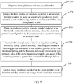
- FIG. 7 is a flowchart of a shielding member production method according to an implementation manner of the present invention. Also with reference to FIG. 1 , the shielding member production method includes the following steps:
- the method further includes: Step 240: Form, in the through hole or slot 11 in an injection molding manner by using a plastic material, a buckling portion 32 and a fastening portion 34 connected to the buckling portion 32, where the fastening portion 34 and the blocking portion 31 are separately disposed on two opposite sides of the metal member 10, and a size of the fastening portion 34 is greater than a size of the through hole or slot 11.
- the enclosing portion 33 is made of the electrically conductive plastic material, the enclosing portion 33, the blocking portion 31, the buckling portion 32, and the fastening portion 34 are formed on the metal member 10 by means of one-off injection molding.
- the method further includes: Step 250: Form, on the metal member 10 in an injection molding manner by using a plastic insulation material, a plastic insulation member used for antenna design.
- the blocking portion 31 configured to block the through hole or slot 11 on the metal member 10 and the enclosing portion 33 disposed around the electronic component 21 are disposed, where one end of the enclosing portion 33 is in contact with the metal member 10, and the other end of the enclosing portion 33 is in contact with the circuit board 20.
- Ground copper is disposed on the circuit board 20 and the enclosing portion 33 is made of an electrically conductive material, and therefore, an electromagnetic wave generated on the metal member 10 is transferred to the ground copper of the circuit board 20 by using the enclosing portion 33, to be conducted away, so that shielding space enclosing the electronic component 21 is formed, so as to reduce or prevent outward radiation of the electromagnetic wave generated by the electronic component 21, thereby preventing operation of another electronic component from being affected.
- a thickness of the stamped metal member or a thickness of the forged metal member is less than a thickness of the diecasting metal member, and therefore, even after the shielding member 30 is formed on the metal member 10, a sum of a thickness of the metal member 10 and a thickness of the shielding member 30 is also less than a sum of the thickness of the diecasting metal member and a thickness of an electrically conductive film. Therefore, the foregoing electronic device 100 resolves a technical problem in the prior art that, because the thickness of the diecasting metal member itself is relatively large, sticking the electrically conductive film on the hole or slot of the diecasting metal member further increases a thickness of the electronic device.
Landscapes
- Engineering & Computer Science (AREA)
- Physics & Mathematics (AREA)
- Computer Hardware Design (AREA)
- Theoretical Computer Science (AREA)
- Microelectronics & Electronic Packaging (AREA)
- General Engineering & Computer Science (AREA)
- Electromagnetism (AREA)
- Human Computer Interaction (AREA)
- General Physics & Mathematics (AREA)
- Power Engineering (AREA)
- Mechanical Engineering (AREA)
- Manufacturing & Machinery (AREA)
- Shielding Devices Or Components To Electric Or Magnetic Fields (AREA)
Claims (7)
- Elektronische Vorrichtung (100), wobei die elektronische Vorrichtung (100) umfasst:ein Metallelement (10), wobei ein Durchgangsloch oder Schlitz (11) auf dem Metallelement (10) angeordnet ist, und das Metallelement (10) ein gestanztes Metallelement (10) oder ein geschmiedetes Metallelement (10) ist;eine Leiterplatte (20), wobei ein elektronisches Bauelement (22) auf der Leiterplatte (20) angeordnet ist; undein Abschirmelement (30), wobei das Abschirmelement (30) einen Blockierabschnitt (31) und einen Umschließungsabschnitt (33) aufweist, wobei der Blockierabschnitt (31) aus einem elektrisch leitenden Kunststoffmaterial hergestellt ist, wobei der Umschließungsabschnitt (33) aus einem Metallmaterial oder einem elektrisch leitenden Kunststoffmaterial hergestellt ist; wobei der Blockierabschnitt (31) dazu ausgelegt ist, das Durchgangsloch oder den Schlitz (11) zu blockieren, der Umschließungsabschnitt (33) um das elektronische Bauelement (22) herum angeordnet ist, ein Ende des Umschließungsabschnitts (33) elektrisch mit dem Metallelement (10) verbunden ist und das andere Ende des Umschließungsabschnitts (33) elektrisch mit dem geerdeten Kupfer der Leiterplatte (20) verbunden ist; wobei das Metallelement (10), der Umschließungsabschnitt (33) und die Leiterplatte (20) einen Abschirmraum bilden und das elektronische Bauelement (22) in dem Abschirmraum angeordnet ist; oder das Metallelement (10), der Blockierabschnitt (31), der Umschließungsabschnitt (33) und die Leiterplatte (20) einen Abschirmraum bilden und das elektronische Bauelement (22) sich in dem Abschirmraum befindet,wobei das Abschirmelement (30) ferner einen mit dem Blockierabschnitt (31) verbundenen Knickabschnitt (32) umfasst, wobei der Knickabschnitt (32) in dem Durchgangsloch oder Schlitz (11) geknickt ist, und einen mit dem Knickabschnitt (32) verbundenen Befestigungsabschnitt (34) umfasst und eine Größe des Befestigungsabschnitts (34) größer als eine Größe des Durchgangslochs oder Schlitzes (11) ist,wobei ein elektrisch leitendes elastisches Element (40) zwischen dem Umschließungsabschnitt (33) und der Leiterplatte (20) oder zwischen dem Umschließungsabschnitt (33) und dem Metallelement (10) angeordnet ist.
- Elektronische Vorrichtung (100) nach Anspruch 1, wobei die elektronische Vorrichtung (100) ferner einen Verstärkungsabschnitt umfasst, der dazu ausgelegt ist, die Festigkeit des Metallelements (10) zu erhöhen, und an dem Metallelement (10) befestigt ist.
- Elektronische Vorrichtung (100) nach Anspruch 2, wobei der Verstärkungsabschnitt gegenüber dem elektronischen Bauelement (22) angeordnet ist.
- Elektronische Vorrichtung (100) nach einem der Ansprüche 1 bis 3, wobei das Durchgangsloch oder der Schlitz (11) gegenüber dem elektronischen Bauelement (22) angeordnet ist.
- Elektronische Vorrichtung (100) nach einem der Ansprüche 1 bis 4, wobei das elektrisch leitende Kunststoffmaterial ein konkret elektrisch und thermisch leitender Kunststoff ist.
- Elektronische Vorrichtung (100) nach einem der Ansprüche 1 bis 5, wobei eine Isolierschicht auf einer von dem Metallelement (10) entfernten Oberfläche des Blockierabschnitts (31) angeordnet ist.
- Elektronische Vorrichtung (100) nach einem der Ansprüche 1 bis 6, wobei der Blockierabschnitt (31) und der Umschließungsabschnitt (33) einstückig spritzgegossen sind, oder der Blockierabschnitt (31), der Umschließungsabschnitt (33) und das Metallelement (10) einstückig spritzgegossen sind.
Applications Claiming Priority (1)
| Application Number | Priority Date | Filing Date | Title |
|---|---|---|---|
| PCT/CN2014/073401 WO2015135186A1 (zh) | 2014-03-13 | 2014-03-13 | 一种电子设备及屏蔽件的制作方法 |
Publications (3)
| Publication Number | Publication Date |
|---|---|
| EP2943049A1 EP2943049A1 (de) | 2015-11-11 |
| EP2943049A4 EP2943049A4 (de) | 2016-03-16 |
| EP2943049B1 true EP2943049B1 (de) | 2020-10-07 |
Family
ID=53732400
Family Applications (1)
| Application Number | Title | Priority Date | Filing Date |
|---|---|---|---|
| EP14868704.9A Active EP2943049B1 (de) | 2014-03-13 | 2014-03-13 | Elektronische vorrichtung |
Country Status (5)
| Country | Link |
|---|---|
| US (1) | US9807918B2 (de) |
| EP (1) | EP2943049B1 (de) |
| JP (1) | JP6229215B2 (de) |
| CN (1) | CN104823532B (de) |
| WO (1) | WO2015135186A1 (de) |
Families Citing this family (14)
| Publication number | Priority date | Publication date | Assignee | Title |
|---|---|---|---|---|
| CN205124242U (zh) * | 2015-10-16 | 2016-03-30 | 中兴通讯股份有限公司 | 一种电子设备 |
| CN105467648A (zh) * | 2016-01-29 | 2016-04-06 | 京东方科技集团股份有限公司 | 背板组件和具有该背板组件的显示装置 |
| CN106210200B (zh) * | 2016-08-25 | 2019-05-10 | Oppo广东移动通信有限公司 | 移动终端、壳体组件及其制造方法 |
| ES2715974T3 (es) | 2016-08-25 | 2019-06-07 | Guangdong Oppo Mobile Telecommunications Corp Ltd | Terminal móvil, componente de carcasa y método de fabricación del mismo |
| CN106912191B (zh) * | 2017-03-16 | 2018-10-19 | 慧谷人工智能研究院(南京)有限公司 | 基于柔性阵列式吸波结构的视频通讯终端 |
| CN107787176A (zh) * | 2017-10-19 | 2018-03-09 | 广东欧珀移动通信有限公司 | 屏蔽罩、电路板组件及移动终端 |
| CN108828629A (zh) * | 2018-06-22 | 2018-11-16 | 安徽尼古拉电子科技有限公司 | 一种基于北斗卫星的抗干扰装置 |
| JP6379319B1 (ja) * | 2018-06-28 | 2018-08-22 | デクセリアルズ株式会社 | 半導体装置 |
| CN109714426A (zh) * | 2019-01-09 | 2019-05-03 | 田凤香 | 网络程序自动下载方法 |
| TWI739245B (zh) * | 2019-03-12 | 2021-09-11 | 仁寶電腦工業股份有限公司 | 殼體結構及其製造方法 |
| CN111800995B (zh) * | 2019-04-09 | 2023-02-28 | 北京小米移动软件有限公司 | 屏蔽罩结构及电子设备 |
| US11343934B2 (en) * | 2019-08-23 | 2022-05-24 | Dell Products L.P. | Mechanical clip lock for an information handling system |
| CN115696888A (zh) * | 2021-07-22 | 2023-02-03 | 启碁科技股份有限公司 | 屏蔽结构及其制造方法 |
| CN113923966A (zh) * | 2021-10-20 | 2022-01-11 | Oppo广东移动通信有限公司 | 电路板组件及电子设备 |
Family Cites Families (23)
| Publication number | Priority date | Publication date | Assignee | Title |
|---|---|---|---|---|
| US4717990A (en) * | 1986-05-30 | 1988-01-05 | Motorola, Inc. | Double-shielded housing for RF circuitry |
| US5574628A (en) * | 1995-05-17 | 1996-11-12 | The Whitaker Corporation | Rigid PCMCIA frame kit |
| JPH1197874A (ja) * | 1997-09-19 | 1999-04-09 | Fujitsu General Ltd | 電子機器のシールド構造 |
| GB9902056D0 (en) * | 1999-01-29 | 1999-03-24 | Neopost Ltd | Secure housing |
| JP3270028B2 (ja) * | 1999-09-10 | 2002-04-02 | 株式会社ソニー・コンピュータエンタテインメント | 電磁シールド板、電磁シールド構造体及びエンタテインメント装置 |
| JP2001244127A (ja) * | 2000-02-29 | 2001-09-07 | Murata Mfg Co Ltd | 高周波部品および通信装置 |
| US6243274B1 (en) * | 2000-04-20 | 2001-06-05 | Redcom Laboratories, Inc. | Shields for electronic components with ready access to shielded components |
| US6949706B2 (en) | 2001-09-28 | 2005-09-27 | Siemens Information And Communication Mobile, Llc | Radio frequency shield for electronic equipment |
| CN1707698A (zh) * | 2004-06-12 | 2005-12-14 | 鸿富锦精密工业(深圳)有限公司 | 可屏蔽电磁干扰的电子装置 |
| US7087835B2 (en) * | 2004-10-19 | 2006-08-08 | Bi-Link Metal Specialties Inc. | Apparatus and method for shielding printed circuit boards |
| CN1849052A (zh) * | 2005-04-05 | 2006-10-18 | 鸿富锦精密工业(深圳)有限公司 | 电磁干扰屏蔽封装体及其制程 |
| CN2862614Y (zh) * | 2005-07-29 | 2007-01-24 | 林江俊 | 防电磁干扰遮蔽罩结构 |
| US7518880B1 (en) * | 2006-02-08 | 2009-04-14 | Bi-Link | Shielding arrangement for electronic device |
| WO2007094068A1 (ja) * | 2006-02-16 | 2007-08-23 | Matsushita Electric Industrial Co., Ltd. | 回路基板 |
| CN100502626C (zh) * | 2006-04-03 | 2009-06-17 | 华冠通讯股份有限公司 | 手持式通讯装置 |
| JP2008084964A (ja) * | 2006-09-26 | 2008-04-10 | Alps Electric Co Ltd | 高周波ユニットの製造方法、及び高周波ユニット |
| US7729500B2 (en) * | 2006-12-19 | 2010-06-01 | Fortmedia, Inc. | Microphone array with electromagnetic interference shielding means |
| JP2009218432A (ja) * | 2008-03-11 | 2009-09-24 | Sharp Corp | 高周波モジュールおよび高周波モジュールの製造方法 |
| CN101578033B (zh) * | 2008-05-09 | 2011-07-20 | 莱尔德电子材料(深圳)有限公司 | 屏蔽装置和制造屏蔽装置的方法 |
| CN101652057B (zh) * | 2008-08-13 | 2012-12-19 | 深圳富泰宏精密工业有限公司 | 屏蔽罩结构 |
| US20100257732A1 (en) * | 2009-04-14 | 2010-10-14 | Ziberna Frank J | Shielding Arrangement for Electronic Device |
| CN201766809U (zh) * | 2010-08-24 | 2011-03-16 | 中兴通讯股份有限公司 | 一种电子通信设备系统及电磁屏蔽装置 |
| CN202634996U (zh) * | 2012-04-24 | 2012-12-26 | 亚旭电子科技(江苏)有限公司 | 电磁波屏蔽罩 |
-
2014
- 2014-03-13 EP EP14868704.9A patent/EP2943049B1/de active Active
- 2014-03-13 JP JP2016506762A patent/JP6229215B2/ja active Active
- 2014-03-13 CN CN201480003096.5A patent/CN104823532B/zh active Active
- 2014-03-13 WO PCT/CN2014/073401 patent/WO2015135186A1/zh not_active Ceased
-
2015
- 2015-07-06 US US14/791,726 patent/US9807918B2/en active Active
Non-Patent Citations (1)
| Title |
|---|
| None * |
Also Published As
| Publication number | Publication date |
|---|---|
| EP2943049A1 (de) | 2015-11-11 |
| EP2943049A4 (de) | 2016-03-16 |
| JP6229215B2 (ja) | 2017-11-15 |
| US20150313045A1 (en) | 2015-10-29 |
| WO2015135186A1 (zh) | 2015-09-17 |
| CN104823532B (zh) | 2019-04-30 |
| US9807918B2 (en) | 2017-10-31 |
| JP2016516308A (ja) | 2016-06-02 |
| CN104823532A (zh) | 2015-08-05 |
Similar Documents
| Publication | Publication Date | Title |
|---|---|---|
| EP2943049B1 (de) | Elektronische vorrichtung | |
| KR102142397B1 (ko) | 이동 단말기 및 방열 및 차폐 구조체 | |
| JP5939102B2 (ja) | 電子機器 | |
| EP2509403B1 (de) | Anordnungen und Verfahren zur Wärmeableitung von tragbaren elektronischen Vorrichtungen | |
| EP1240811B1 (de) | Tragrahmen eines wärmeleitenden materials | |
| US7486517B2 (en) | Hand-held portable electronic device having a heat spreader | |
| US9705553B2 (en) | Mobile terminal with waterproof sheet and manufacturing method | |
| EP3261173B1 (de) | Kommunikationsvorrichtung und antennenanordnung dafür | |
| EP4060807B1 (de) | Tragbare elektronische vorrichtung | |
| EP3686768A1 (de) | Fingerabdruckerkennungsmodul und endgerätevorrichtung | |
| US20130077282A1 (en) | Integrated thermal and emi shields and methods for making the same | |
| US10999957B2 (en) | Communication module and mounting structure thereof | |
| KR20190019901A (ko) | 케이스 및 케이스의 제조 방법 | |
| JP2006319134A (ja) | 放熱構造 | |
| CN110535248B (zh) | 移动终端、无线充电模组及其制备方法 | |
| US20130170127A1 (en) | Memory assembly | |
| CN110418562A (zh) | 一种屏蔽罩及电子设备 | |
| JP2013171932A (ja) | 電子機器の放熱装置 | |
| CN101507045A (zh) | 便携式设备 | |
| CN203481390U (zh) | 一种用于电子设备的铁氧体模块 | |
| JP2011187844A (ja) | 電子装置及びシールド部材 | |
| CN222216343U (zh) | 电子设备 | |
| CN111315191B (zh) | 散热机构、显示装置及电子设备 | |
| EP4503341A1 (de) | Verbindungsstruktur und elektronische vorrichtung | |
| CN204335204U (zh) | 终端 |
Legal Events
| Date | Code | Title | Description |
|---|---|---|---|
| PUAI | Public reference made under article 153(3) epc to a published international application that has entered the european phase |
Free format text: ORIGINAL CODE: 0009012 |
|
| 17P | Request for examination filed |
Effective date: 20150612 |
|
| AK | Designated contracting states |
Kind code of ref document: A1 Designated state(s): AL AT BE BG CH CY CZ DE DK EE ES FI FR GB GR HR HU IE IS IT LI LT LU LV MC MK MT NL NO PL PT RO RS SE SI SK SM TR |
|
| AX | Request for extension of the european patent |
Extension state: BA ME |
|
| A4 | Supplementary search report drawn up and despatched |
Effective date: 20160212 |
|
| RIC1 | Information provided on ipc code assigned before grant |
Ipc: H05K 9/00 20060101AFI20160208BHEP |
|
| DAX | Request for extension of the european patent (deleted) | ||
| RAP1 | Party data changed (applicant data changed or rights of an application transferred) |
Owner name: HUAWEI DEVICE (DONGGUAN) CO., LTD. |
|
| STAA | Information on the status of an ep patent application or granted ep patent |
Free format text: STATUS: EXAMINATION IS IN PROGRESS |
|
| 17Q | First examination report despatched |
Effective date: 20180703 |
|
| RAP1 | Party data changed (applicant data changed or rights of an application transferred) |
Owner name: HUAWEI DEVICE CO., LTD. |
|
| GRAP | Despatch of communication of intention to grant a patent |
Free format text: ORIGINAL CODE: EPIDOSNIGR1 |
|
| STAA | Information on the status of an ep patent application or granted ep patent |
Free format text: STATUS: GRANT OF PATENT IS INTENDED |
|
| INTG | Intention to grant announced |
Effective date: 20200430 |
|
| GRAS | Grant fee paid |
Free format text: ORIGINAL CODE: EPIDOSNIGR3 |
|
| GRAA | (expected) grant |
Free format text: ORIGINAL CODE: 0009210 |
|
| STAA | Information on the status of an ep patent application or granted ep patent |
Free format text: STATUS: THE PATENT HAS BEEN GRANTED |
|
| AK | Designated contracting states |
Kind code of ref document: B1 Designated state(s): AL AT BE BG CH CY CZ DE DK EE ES FI FR GB GR HR HU IE IS IT LI LT LU LV MC MK MT NL NO PL PT RO RS SE SI SK SM TR |
|
| REG | Reference to a national code |
Ref country code: GB Ref legal event code: FG4D |
|
| REG | Reference to a national code |
Ref country code: CH Ref legal event code: EP Ref country code: AT Ref legal event code: REF Ref document number: 1322622 Country of ref document: AT Kind code of ref document: T Effective date: 20201015 |
|
| REG | Reference to a national code |
Ref country code: IE Ref legal event code: FG4D |
|
| REG | Reference to a national code |
Ref country code: DE Ref legal event code: R096 Ref document number: 602014071101 Country of ref document: DE |
|
| REG | Reference to a national code |
Ref country code: NL Ref legal event code: FP |
|
| REG | Reference to a national code |
Ref country code: AT Ref legal event code: MK05 Ref document number: 1322622 Country of ref document: AT Kind code of ref document: T Effective date: 20201007 |
|
| PG25 | Lapsed in a contracting state [announced via postgrant information from national office to epo] |
Ref country code: GR Free format text: LAPSE BECAUSE OF FAILURE TO SUBMIT A TRANSLATION OF THE DESCRIPTION OR TO PAY THE FEE WITHIN THE PRESCRIBED TIME-LIMIT Effective date: 20210108 Ref country code: NO Free format text: LAPSE BECAUSE OF FAILURE TO SUBMIT A TRANSLATION OF THE DESCRIPTION OR TO PAY THE FEE WITHIN THE PRESCRIBED TIME-LIMIT Effective date: 20210107 Ref country code: PT Free format text: LAPSE BECAUSE OF FAILURE TO SUBMIT A TRANSLATION OF THE DESCRIPTION OR TO PAY THE FEE WITHIN THE PRESCRIBED TIME-LIMIT Effective date: 20210208 Ref country code: RS Free format text: LAPSE BECAUSE OF FAILURE TO SUBMIT A TRANSLATION OF THE DESCRIPTION OR TO PAY THE FEE WITHIN THE PRESCRIBED TIME-LIMIT Effective date: 20201007 Ref country code: FI Free format text: LAPSE BECAUSE OF FAILURE TO SUBMIT A TRANSLATION OF THE DESCRIPTION OR TO PAY THE FEE WITHIN THE PRESCRIBED TIME-LIMIT Effective date: 20201007 |
|
| REG | Reference to a national code |
Ref country code: LT Ref legal event code: MG4D |
|
| PG25 | Lapsed in a contracting state [announced via postgrant information from national office to epo] |
Ref country code: LV Free format text: LAPSE BECAUSE OF FAILURE TO SUBMIT A TRANSLATION OF THE DESCRIPTION OR TO PAY THE FEE WITHIN THE PRESCRIBED TIME-LIMIT Effective date: 20201007 Ref country code: PL Free format text: LAPSE BECAUSE OF FAILURE TO SUBMIT A TRANSLATION OF THE DESCRIPTION OR TO PAY THE FEE WITHIN THE PRESCRIBED TIME-LIMIT Effective date: 20201007 Ref country code: IS Free format text: LAPSE BECAUSE OF FAILURE TO SUBMIT A TRANSLATION OF THE DESCRIPTION OR TO PAY THE FEE WITHIN THE PRESCRIBED TIME-LIMIT Effective date: 20210207 Ref country code: SE Free format text: LAPSE BECAUSE OF FAILURE TO SUBMIT A TRANSLATION OF THE DESCRIPTION OR TO PAY THE FEE WITHIN THE PRESCRIBED TIME-LIMIT Effective date: 20201007 Ref country code: BG Free format text: LAPSE BECAUSE OF FAILURE TO SUBMIT A TRANSLATION OF THE DESCRIPTION OR TO PAY THE FEE WITHIN THE PRESCRIBED TIME-LIMIT Effective date: 20210107 Ref country code: AT Free format text: LAPSE BECAUSE OF FAILURE TO SUBMIT A TRANSLATION OF THE DESCRIPTION OR TO PAY THE FEE WITHIN THE PRESCRIBED TIME-LIMIT Effective date: 20201007 Ref country code: ES Free format text: LAPSE BECAUSE OF FAILURE TO SUBMIT A TRANSLATION OF THE DESCRIPTION OR TO PAY THE FEE WITHIN THE PRESCRIBED TIME-LIMIT Effective date: 20201007 |
|
| PG25 | Lapsed in a contracting state [announced via postgrant information from national office to epo] |
Ref country code: HR Free format text: LAPSE BECAUSE OF FAILURE TO SUBMIT A TRANSLATION OF THE DESCRIPTION OR TO PAY THE FEE WITHIN THE PRESCRIBED TIME-LIMIT Effective date: 20201007 |
|
| REG | Reference to a national code |
Ref country code: DE Ref legal event code: R097 Ref document number: 602014071101 Country of ref document: DE |
|
| PG25 | Lapsed in a contracting state [announced via postgrant information from national office to epo] |
Ref country code: RO Free format text: LAPSE BECAUSE OF FAILURE TO SUBMIT A TRANSLATION OF THE DESCRIPTION OR TO PAY THE FEE WITHIN THE PRESCRIBED TIME-LIMIT Effective date: 20201007 Ref country code: SK Free format text: LAPSE BECAUSE OF FAILURE TO SUBMIT A TRANSLATION OF THE DESCRIPTION OR TO PAY THE FEE WITHIN THE PRESCRIBED TIME-LIMIT Effective date: 20201007 Ref country code: LT Free format text: LAPSE BECAUSE OF FAILURE TO SUBMIT A TRANSLATION OF THE DESCRIPTION OR TO PAY THE FEE WITHIN THE PRESCRIBED TIME-LIMIT Effective date: 20201007 Ref country code: SM Free format text: LAPSE BECAUSE OF FAILURE TO SUBMIT A TRANSLATION OF THE DESCRIPTION OR TO PAY THE FEE WITHIN THE PRESCRIBED TIME-LIMIT Effective date: 20201007 Ref country code: CZ Free format text: LAPSE BECAUSE OF FAILURE TO SUBMIT A TRANSLATION OF THE DESCRIPTION OR TO PAY THE FEE WITHIN THE PRESCRIBED TIME-LIMIT Effective date: 20201007 Ref country code: EE Free format text: LAPSE BECAUSE OF FAILURE TO SUBMIT A TRANSLATION OF THE DESCRIPTION OR TO PAY THE FEE WITHIN THE PRESCRIBED TIME-LIMIT Effective date: 20201007 |
|
| PLBE | No opposition filed within time limit |
Free format text: ORIGINAL CODE: 0009261 |
|
| STAA | Information on the status of an ep patent application or granted ep patent |
Free format text: STATUS: NO OPPOSITION FILED WITHIN TIME LIMIT |
|
| PG25 | Lapsed in a contracting state [announced via postgrant information from national office to epo] |
Ref country code: DK Free format text: LAPSE BECAUSE OF FAILURE TO SUBMIT A TRANSLATION OF THE DESCRIPTION OR TO PAY THE FEE WITHIN THE PRESCRIBED TIME-LIMIT Effective date: 20201007 |
|
| 26N | No opposition filed |
Effective date: 20210708 |
|
| PG25 | Lapsed in a contracting state [announced via postgrant information from national office to epo] |
Ref country code: IT Free format text: LAPSE BECAUSE OF FAILURE TO SUBMIT A TRANSLATION OF THE DESCRIPTION OR TO PAY THE FEE WITHIN THE PRESCRIBED TIME-LIMIT Effective date: 20201007 Ref country code: AL Free format text: LAPSE BECAUSE OF FAILURE TO SUBMIT A TRANSLATION OF THE DESCRIPTION OR TO PAY THE FEE WITHIN THE PRESCRIBED TIME-LIMIT Effective date: 20201007 Ref country code: MC Free format text: LAPSE BECAUSE OF FAILURE TO SUBMIT A TRANSLATION OF THE DESCRIPTION OR TO PAY THE FEE WITHIN THE PRESCRIBED TIME-LIMIT Effective date: 20201007 |
|
| REG | Reference to a national code |
Ref country code: CH Ref legal event code: PL |
|
| PG25 | Lapsed in a contracting state [announced via postgrant information from national office to epo] |
Ref country code: SI Free format text: LAPSE BECAUSE OF FAILURE TO SUBMIT A TRANSLATION OF THE DESCRIPTION OR TO PAY THE FEE WITHIN THE PRESCRIBED TIME-LIMIT Effective date: 20201007 |
|
| REG | Reference to a national code |
Ref country code: BE Ref legal event code: MM Effective date: 20210331 |
|
| PG25 | Lapsed in a contracting state [announced via postgrant information from national office to epo] |
Ref country code: IE Free format text: LAPSE BECAUSE OF NON-PAYMENT OF DUE FEES Effective date: 20210313 Ref country code: LI Free format text: LAPSE BECAUSE OF NON-PAYMENT OF DUE FEES Effective date: 20210331 Ref country code: LU Free format text: LAPSE BECAUSE OF NON-PAYMENT OF DUE FEES Effective date: 20210313 Ref country code: CH Free format text: LAPSE BECAUSE OF NON-PAYMENT OF DUE FEES Effective date: 20210331 |
|
| PG25 | Lapsed in a contracting state [announced via postgrant information from national office to epo] |
Ref country code: IS Free format text: LAPSE BECAUSE OF FAILURE TO SUBMIT A TRANSLATION OF THE DESCRIPTION OR TO PAY THE FEE WITHIN THE PRESCRIBED TIME-LIMIT Effective date: 20210207 |
|
| PG25 | Lapsed in a contracting state [announced via postgrant information from national office to epo] |
Ref country code: BE Free format text: LAPSE BECAUSE OF NON-PAYMENT OF DUE FEES Effective date: 20210331 |
|
| PG25 | Lapsed in a contracting state [announced via postgrant information from national office to epo] |
Ref country code: HU Free format text: LAPSE BECAUSE OF FAILURE TO SUBMIT A TRANSLATION OF THE DESCRIPTION OR TO PAY THE FEE WITHIN THE PRESCRIBED TIME-LIMIT; INVALID AB INITIO Effective date: 20140313 |
|
| PG25 | Lapsed in a contracting state [announced via postgrant information from national office to epo] |
Ref country code: CY Free format text: LAPSE BECAUSE OF FAILURE TO SUBMIT A TRANSLATION OF THE DESCRIPTION OR TO PAY THE FEE WITHIN THE PRESCRIBED TIME-LIMIT Effective date: 20201007 |
|
| PG25 | Lapsed in a contracting state [announced via postgrant information from national office to epo] |
Ref country code: MK Free format text: LAPSE BECAUSE OF FAILURE TO SUBMIT A TRANSLATION OF THE DESCRIPTION OR TO PAY THE FEE WITHIN THE PRESCRIBED TIME-LIMIT Effective date: 20201007 |
|
| PG25 | Lapsed in a contracting state [announced via postgrant information from national office to epo] |
Ref country code: TR Free format text: LAPSE BECAUSE OF FAILURE TO SUBMIT A TRANSLATION OF THE DESCRIPTION OR TO PAY THE FEE WITHIN THE PRESCRIBED TIME-LIMIT Effective date: 20201007 |
|
| PG25 | Lapsed in a contracting state [announced via postgrant information from national office to epo] |
Ref country code: MT Free format text: LAPSE BECAUSE OF FAILURE TO SUBMIT A TRANSLATION OF THE DESCRIPTION OR TO PAY THE FEE WITHIN THE PRESCRIBED TIME-LIMIT Effective date: 20201007 |
|
| PGFP | Annual fee paid to national office [announced via postgrant information from national office to epo] |
Ref country code: DE Payment date: 20250204 Year of fee payment: 12 |
|
| PGFP | Annual fee paid to national office [announced via postgrant information from national office to epo] |
Ref country code: FR Payment date: 20250210 Year of fee payment: 12 |
|
| PGFP | Annual fee paid to national office [announced via postgrant information from national office to epo] |
Ref country code: GB Payment date: 20250130 Year of fee payment: 12 |
|
| PGFP | Annual fee paid to national office [announced via postgrant information from national office to epo] |
Ref country code: NL Payment date: 20260213 Year of fee payment: 13 |