EP2942789A2 - Nichtlineares resistives spannungselement und verfahren zur herstellung davon - Google Patents
Nichtlineares resistives spannungselement und verfahren zur herstellung davon Download PDFInfo
- Publication number
- EP2942789A2 EP2942789A2 EP15159822.4A EP15159822A EP2942789A2 EP 2942789 A2 EP2942789 A2 EP 2942789A2 EP 15159822 A EP15159822 A EP 15159822A EP 2942789 A2 EP2942789 A2 EP 2942789A2
- Authority
- EP
- European Patent Office
- Prior art keywords
- rare
- zinc oxide
- earth metal
- metal oxide
- voltage nonlinear
- Prior art date
- Legal status (The legal status is an assumption and is not a legal conclusion. Google has not performed a legal analysis and makes no representation as to the accuracy of the status listed.)
- Granted
Links
Images

Classifications
-
- H—ELECTRICITY
- H01—ELECTRIC ELEMENTS
- H01C—RESISTORS
- H01C7/00—Non-adjustable resistors formed as one or more layers or coatings; Non-adjustable resistors made from powdered conducting material or powdered semi-conducting material with or without insulating material
- H01C7/10—Non-adjustable resistors formed as one or more layers or coatings; Non-adjustable resistors made from powdered conducting material or powdered semi-conducting material with or without insulating material voltage responsive, i.e. varistors
- H01C7/105—Varistor cores
- H01C7/108—Metal oxide
- H01C7/112—ZnO type
-
- C—CHEMISTRY; METALLURGY
- C04—CEMENTS; CONCRETE; ARTIFICIAL STONE; CERAMICS; REFRACTORIES
- C04B—LIME, MAGNESIA; SLAG; CEMENTS; COMPOSITIONS THEREOF, e.g. MORTARS, CONCRETE OR LIKE BUILDING MATERIALS; ARTIFICIAL STONE; CERAMICS; REFRACTORIES; TREATMENT OF NATURAL STONE
- C04B35/00—Shaped ceramic products characterised by their composition; Ceramics compositions; Processing powders of inorganic compounds preparatory to the manufacturing of ceramic products
- C04B35/01—Shaped ceramic products characterised by their composition; Ceramics compositions; Processing powders of inorganic compounds preparatory to the manufacturing of ceramic products based on oxide ceramics
- C04B35/453—Shaped ceramic products characterised by their composition; Ceramics compositions; Processing powders of inorganic compounds preparatory to the manufacturing of ceramic products based on oxide ceramics based on zinc, tin, or bismuth oxides or solid solutions thereof with other oxides, e.g. zincates, stannates or bismuthates
-
- C—CHEMISTRY; METALLURGY
- C04—CEMENTS; CONCRETE; ARTIFICIAL STONE; CERAMICS; REFRACTORIES
- C04B—LIME, MAGNESIA; SLAG; CEMENTS; COMPOSITIONS THEREOF, e.g. MORTARS, CONCRETE OR LIKE BUILDING MATERIALS; ARTIFICIAL STONE; CERAMICS; REFRACTORIES; TREATMENT OF NATURAL STONE
- C04B35/00—Shaped ceramic products characterised by their composition; Ceramics compositions; Processing powders of inorganic compounds preparatory to the manufacturing of ceramic products
- C04B35/622—Forming processes; Processing powders of inorganic compounds preparatory to the manufacturing of ceramic products
- C04B35/626—Preparing or treating the powders individually or as batches ; preparing or treating macroscopic reinforcing agents for ceramic products, e.g. fibres; mechanical aspects section B
- C04B35/62605—Treating the starting powders individually or as mixtures
- C04B35/62695—Granulation or pelletising
-
- C—CHEMISTRY; METALLURGY
- C04—CEMENTS; CONCRETE; ARTIFICIAL STONE; CERAMICS; REFRACTORIES
- C04B—LIME, MAGNESIA; SLAG; CEMENTS; COMPOSITIONS THEREOF, e.g. MORTARS, CONCRETE OR LIKE BUILDING MATERIALS; ARTIFICIAL STONE; CERAMICS; REFRACTORIES; TREATMENT OF NATURAL STONE
- C04B37/00—Joining burned ceramic articles with other burned ceramic articles or other articles by heating
- C04B37/003—Joining burned ceramic articles with other burned ceramic articles or other articles by heating by means of an interlayer consisting of a combination of materials selected from glass, or ceramic material with metals, metal oxides or metal salts
-
- C—CHEMISTRY; METALLURGY
- C04—CEMENTS; CONCRETE; ARTIFICIAL STONE; CERAMICS; REFRACTORIES
- C04B—LIME, MAGNESIA; SLAG; CEMENTS; COMPOSITIONS THEREOF, e.g. MORTARS, CONCRETE OR LIKE BUILDING MATERIALS; ARTIFICIAL STONE; CERAMICS; REFRACTORIES; TREATMENT OF NATURAL STONE
- C04B37/00—Joining burned ceramic articles with other burned ceramic articles or other articles by heating
- C04B37/003—Joining burned ceramic articles with other burned ceramic articles or other articles by heating by means of an interlayer consisting of a combination of materials selected from glass, or ceramic material with metals, metal oxides or metal salts
- C04B37/005—Joining burned ceramic articles with other burned ceramic articles or other articles by heating by means of an interlayer consisting of a combination of materials selected from glass, or ceramic material with metals, metal oxides or metal salts consisting of glass or ceramic material
-
- C—CHEMISTRY; METALLURGY
- C04—CEMENTS; CONCRETE; ARTIFICIAL STONE; CERAMICS; REFRACTORIES
- C04B—LIME, MAGNESIA; SLAG; CEMENTS; COMPOSITIONS THEREOF, e.g. MORTARS, CONCRETE OR LIKE BUILDING MATERIALS; ARTIFICIAL STONE; CERAMICS; REFRACTORIES; TREATMENT OF NATURAL STONE
- C04B37/00—Joining burned ceramic articles with other burned ceramic articles or other articles by heating
- C04B37/003—Joining burned ceramic articles with other burned ceramic articles or other articles by heating by means of an interlayer consisting of a combination of materials selected from glass, or ceramic material with metals, metal oxides or metal salts
- C04B37/006—Joining burned ceramic articles with other burned ceramic articles or other articles by heating by means of an interlayer consisting of a combination of materials selected from glass, or ceramic material with metals, metal oxides or metal salts consisting of metals or metal salts
-
- H—ELECTRICITY
- H01—ELECTRIC ELEMENTS
- H01C—RESISTORS
- H01C17/00—Apparatus or processes specially adapted for manufacturing resistors
-
- H—ELECTRICITY
- H01—ELECTRIC ELEMENTS
- H01C—RESISTORS
- H01C7/00—Non-adjustable resistors formed as one or more layers or coatings; Non-adjustable resistors made from powdered conducting material or powdered semi-conducting material with or without insulating material
- H01C7/10—Non-adjustable resistors formed as one or more layers or coatings; Non-adjustable resistors made from powdered conducting material or powdered semi-conducting material with or without insulating material voltage responsive, i.e. varistors
-
- H—ELECTRICITY
- H01—ELECTRIC ELEMENTS
- H01C—RESISTORS
- H01C7/00—Non-adjustable resistors formed as one or more layers or coatings; Non-adjustable resistors made from powdered conducting material or powdered semi-conducting material with or without insulating material
- H01C7/10—Non-adjustable resistors formed as one or more layers or coatings; Non-adjustable resistors made from powdered conducting material or powdered semi-conducting material with or without insulating material voltage responsive, i.e. varistors
- H01C7/102—Varistor boundary, e.g. surface layers
-
- H—ELECTRICITY
- H01—ELECTRIC ELEMENTS
- H01C—RESISTORS
- H01C7/00—Non-adjustable resistors formed as one or more layers or coatings; Non-adjustable resistors made from powdered conducting material or powdered semi-conducting material with or without insulating material
- H01C7/18—Non-adjustable resistors formed as one or more layers or coatings; Non-adjustable resistors made from powdered conducting material or powdered semi-conducting material with or without insulating material comprising a plurality of layers stacked between terminals
-
- C—CHEMISTRY; METALLURGY
- C04—CEMENTS; CONCRETE; ARTIFICIAL STONE; CERAMICS; REFRACTORIES
- C04B—LIME, MAGNESIA; SLAG; CEMENTS; COMPOSITIONS THEREOF, e.g. MORTARS, CONCRETE OR LIKE BUILDING MATERIALS; ARTIFICIAL STONE; CERAMICS; REFRACTORIES; TREATMENT OF NATURAL STONE
- C04B2235/00—Aspects relating to ceramic starting mixtures or sintered ceramic products
- C04B2235/02—Composition of constituents of the starting material or of secondary phases of the final product
- C04B2235/30—Constituents and secondary phases not being of a fibrous nature
- C04B2235/32—Metal oxides, mixed metal oxides, or oxide-forming salts thereof, e.g. carbonates, nitrates, (oxy)hydroxides, chlorides
- C04B2235/3217—Aluminum oxide or oxide forming salts thereof, e.g. bauxite, alpha-alumina
-
- C—CHEMISTRY; METALLURGY
- C04—CEMENTS; CONCRETE; ARTIFICIAL STONE; CERAMICS; REFRACTORIES
- C04B—LIME, MAGNESIA; SLAG; CEMENTS; COMPOSITIONS THEREOF, e.g. MORTARS, CONCRETE OR LIKE BUILDING MATERIALS; ARTIFICIAL STONE; CERAMICS; REFRACTORIES; TREATMENT OF NATURAL STONE
- C04B2235/00—Aspects relating to ceramic starting mixtures or sintered ceramic products
- C04B2235/02—Composition of constituents of the starting material or of secondary phases of the final product
- C04B2235/30—Constituents and secondary phases not being of a fibrous nature
- C04B2235/32—Metal oxides, mixed metal oxides, or oxide-forming salts thereof, e.g. carbonates, nitrates, (oxy)hydroxides, chlorides
- C04B2235/3217—Aluminum oxide or oxide forming salts thereof, e.g. bauxite, alpha-alumina
- C04B2235/322—Transition aluminas, e.g. delta or gamma aluminas
-
- C—CHEMISTRY; METALLURGY
- C04—CEMENTS; CONCRETE; ARTIFICIAL STONE; CERAMICS; REFRACTORIES
- C04B—LIME, MAGNESIA; SLAG; CEMENTS; COMPOSITIONS THEREOF, e.g. MORTARS, CONCRETE OR LIKE BUILDING MATERIALS; ARTIFICIAL STONE; CERAMICS; REFRACTORIES; TREATMENT OF NATURAL STONE
- C04B2235/00—Aspects relating to ceramic starting mixtures or sintered ceramic products
- C04B2235/02—Composition of constituents of the starting material or of secondary phases of the final product
- C04B2235/30—Constituents and secondary phases not being of a fibrous nature
- C04B2235/32—Metal oxides, mixed metal oxides, or oxide-forming salts thereof, e.g. carbonates, nitrates, (oxy)hydroxides, chlorides
- C04B2235/3284—Zinc oxides, zincates, cadmium oxides, cadmiates, mercury oxides, mercurates or oxide forming salts thereof
-
- C—CHEMISTRY; METALLURGY
- C04—CEMENTS; CONCRETE; ARTIFICIAL STONE; CERAMICS; REFRACTORIES
- C04B—LIME, MAGNESIA; SLAG; CEMENTS; COMPOSITIONS THEREOF, e.g. MORTARS, CONCRETE OR LIKE BUILDING MATERIALS; ARTIFICIAL STONE; CERAMICS; REFRACTORIES; TREATMENT OF NATURAL STONE
- C04B2235/00—Aspects relating to ceramic starting mixtures or sintered ceramic products
- C04B2235/02—Composition of constituents of the starting material or of secondary phases of the final product
- C04B2235/30—Constituents and secondary phases not being of a fibrous nature
- C04B2235/32—Metal oxides, mixed metal oxides, or oxide-forming salts thereof, e.g. carbonates, nitrates, (oxy)hydroxides, chlorides
- C04B2235/3286—Gallium oxides, gallates, indium oxides, indates, thallium oxides, thallates or oxide forming salts thereof, e.g. zinc gallate
-
- C—CHEMISTRY; METALLURGY
- C04—CEMENTS; CONCRETE; ARTIFICIAL STONE; CERAMICS; REFRACTORIES
- C04B—LIME, MAGNESIA; SLAG; CEMENTS; COMPOSITIONS THEREOF, e.g. MORTARS, CONCRETE OR LIKE BUILDING MATERIALS; ARTIFICIAL STONE; CERAMICS; REFRACTORIES; TREATMENT OF NATURAL STONE
- C04B2235/00—Aspects relating to ceramic starting mixtures or sintered ceramic products
- C04B2235/02—Composition of constituents of the starting material or of secondary phases of the final product
- C04B2235/30—Constituents and secondary phases not being of a fibrous nature
- C04B2235/44—Metal salt constituents or additives chosen for the nature of the anions, e.g. hydrides or acetylacetonate
- C04B2235/443—Nitrates or nitrites
-
- C—CHEMISTRY; METALLURGY
- C04—CEMENTS; CONCRETE; ARTIFICIAL STONE; CERAMICS; REFRACTORIES
- C04B—LIME, MAGNESIA; SLAG; CEMENTS; COMPOSITIONS THEREOF, e.g. MORTARS, CONCRETE OR LIKE BUILDING MATERIALS; ARTIFICIAL STONE; CERAMICS; REFRACTORIES; TREATMENT OF NATURAL STONE
- C04B2235/00—Aspects relating to ceramic starting mixtures or sintered ceramic products
- C04B2235/02—Composition of constituents of the starting material or of secondary phases of the final product
- C04B2235/50—Constituents or additives of the starting mixture chosen for their shape or used because of their shape or their physical appearance
- C04B2235/54—Particle size related information
- C04B2235/5418—Particle size related information expressed by the size of the particles or aggregates thereof
- C04B2235/5436—Particle size related information expressed by the size of the particles or aggregates thereof micrometer sized, i.e. from 1 to 100 micron
-
- C—CHEMISTRY; METALLURGY
- C04—CEMENTS; CONCRETE; ARTIFICIAL STONE; CERAMICS; REFRACTORIES
- C04B—LIME, MAGNESIA; SLAG; CEMENTS; COMPOSITIONS THEREOF, e.g. MORTARS, CONCRETE OR LIKE BUILDING MATERIALS; ARTIFICIAL STONE; CERAMICS; REFRACTORIES; TREATMENT OF NATURAL STONE
- C04B2235/00—Aspects relating to ceramic starting mixtures or sintered ceramic products
- C04B2235/02—Composition of constituents of the starting material or of secondary phases of the final product
- C04B2235/50—Constituents or additives of the starting mixture chosen for their shape or used because of their shape or their physical appearance
- C04B2235/54—Particle size related information
- C04B2235/5418—Particle size related information expressed by the size of the particles or aggregates thereof
- C04B2235/5454—Particle size related information expressed by the size of the particles or aggregates thereof nanometer sized, i.e. below 100 nm
-
- C—CHEMISTRY; METALLURGY
- C04—CEMENTS; CONCRETE; ARTIFICIAL STONE; CERAMICS; REFRACTORIES
- C04B—LIME, MAGNESIA; SLAG; CEMENTS; COMPOSITIONS THEREOF, e.g. MORTARS, CONCRETE OR LIKE BUILDING MATERIALS; ARTIFICIAL STONE; CERAMICS; REFRACTORIES; TREATMENT OF NATURAL STONE
- C04B2235/00—Aspects relating to ceramic starting mixtures or sintered ceramic products
- C04B2235/65—Aspects relating to heat treatments of ceramic bodies such as green ceramics or pre-sintered ceramics, e.g. burning, sintering or melting processes
- C04B2235/658—Atmosphere during thermal treatment
-
- C—CHEMISTRY; METALLURGY
- C04—CEMENTS; CONCRETE; ARTIFICIAL STONE; CERAMICS; REFRACTORIES
- C04B—LIME, MAGNESIA; SLAG; CEMENTS; COMPOSITIONS THEREOF, e.g. MORTARS, CONCRETE OR LIKE BUILDING MATERIALS; ARTIFICIAL STONE; CERAMICS; REFRACTORIES; TREATMENT OF NATURAL STONE
- C04B2235/00—Aspects relating to ceramic starting mixtures or sintered ceramic products
- C04B2235/70—Aspects relating to sintered or melt-casted ceramic products
- C04B2235/96—Properties of ceramic products, e.g. mechanical properties such as strength, toughness, wear resistance
-
- C—CHEMISTRY; METALLURGY
- C04—CEMENTS; CONCRETE; ARTIFICIAL STONE; CERAMICS; REFRACTORIES
- C04B—LIME, MAGNESIA; SLAG; CEMENTS; COMPOSITIONS THEREOF, e.g. MORTARS, CONCRETE OR LIKE BUILDING MATERIALS; ARTIFICIAL STONE; CERAMICS; REFRACTORIES; TREATMENT OF NATURAL STONE
- C04B2237/00—Aspects relating to ceramic laminates or to joining of ceramic articles with other articles by heating
- C04B2237/02—Aspects relating to interlayers, e.g. used to join ceramic articles with other articles by heating
- C04B2237/04—Ceramic interlayers
- C04B2237/06—Oxidic interlayers
-
- C—CHEMISTRY; METALLURGY
- C04—CEMENTS; CONCRETE; ARTIFICIAL STONE; CERAMICS; REFRACTORIES
- C04B—LIME, MAGNESIA; SLAG; CEMENTS; COMPOSITIONS THEREOF, e.g. MORTARS, CONCRETE OR LIKE BUILDING MATERIALS; ARTIFICIAL STONE; CERAMICS; REFRACTORIES; TREATMENT OF NATURAL STONE
- C04B2237/00—Aspects relating to ceramic laminates or to joining of ceramic articles with other articles by heating
- C04B2237/02—Aspects relating to interlayers, e.g. used to join ceramic articles with other articles by heating
- C04B2237/04—Ceramic interlayers
- C04B2237/06—Oxidic interlayers
- C04B2237/066—Oxidic interlayers based on rare earth oxides
-
- C—CHEMISTRY; METALLURGY
- C04—CEMENTS; CONCRETE; ARTIFICIAL STONE; CERAMICS; REFRACTORIES
- C04B—LIME, MAGNESIA; SLAG; CEMENTS; COMPOSITIONS THEREOF, e.g. MORTARS, CONCRETE OR LIKE BUILDING MATERIALS; ARTIFICIAL STONE; CERAMICS; REFRACTORIES; TREATMENT OF NATURAL STONE
- C04B2237/00—Aspects relating to ceramic laminates or to joining of ceramic articles with other articles by heating
- C04B2237/02—Aspects relating to interlayers, e.g. used to join ceramic articles with other articles by heating
- C04B2237/12—Metallic interlayers
- C04B2237/125—Metallic interlayers based on noble metals, e.g. silver
-
- C—CHEMISTRY; METALLURGY
- C04—CEMENTS; CONCRETE; ARTIFICIAL STONE; CERAMICS; REFRACTORIES
- C04B—LIME, MAGNESIA; SLAG; CEMENTS; COMPOSITIONS THEREOF, e.g. MORTARS, CONCRETE OR LIKE BUILDING MATERIALS; ARTIFICIAL STONE; CERAMICS; REFRACTORIES; TREATMENT OF NATURAL STONE
- C04B2237/00—Aspects relating to ceramic laminates or to joining of ceramic articles with other articles by heating
- C04B2237/02—Aspects relating to interlayers, e.g. used to join ceramic articles with other articles by heating
- C04B2237/12—Metallic interlayers
- C04B2237/126—Metallic interlayers wherein the active component for bonding is not the largest fraction of the interlayer
-
- C—CHEMISTRY; METALLURGY
- C04—CEMENTS; CONCRETE; ARTIFICIAL STONE; CERAMICS; REFRACTORIES
- C04B—LIME, MAGNESIA; SLAG; CEMENTS; COMPOSITIONS THEREOF, e.g. MORTARS, CONCRETE OR LIKE BUILDING MATERIALS; ARTIFICIAL STONE; CERAMICS; REFRACTORIES; TREATMENT OF NATURAL STONE
- C04B2237/00—Aspects relating to ceramic laminates or to joining of ceramic articles with other articles by heating
- C04B2237/30—Composition of layers of ceramic laminates or of ceramic or metallic articles to be joined by heating, e.g. Si substrates
- C04B2237/32—Ceramic
- C04B2237/34—Oxidic
-
- C—CHEMISTRY; METALLURGY
- C04—CEMENTS; CONCRETE; ARTIFICIAL STONE; CERAMICS; REFRACTORIES
- C04B—LIME, MAGNESIA; SLAG; CEMENTS; COMPOSITIONS THEREOF, e.g. MORTARS, CONCRETE OR LIKE BUILDING MATERIALS; ARTIFICIAL STONE; CERAMICS; REFRACTORIES; TREATMENT OF NATURAL STONE
- C04B2237/00—Aspects relating to ceramic laminates or to joining of ceramic articles with other articles by heating
- C04B2237/50—Processing aspects relating to ceramic laminates or to the joining of ceramic articles with other articles by heating
- C04B2237/70—Forming laminates or joined articles comprising layers of a specific, unusual thickness
- C04B2237/708—Forming laminates or joined articles comprising layers of a specific, unusual thickness of one or more of the interlayers
-
- C—CHEMISTRY; METALLURGY
- C04—CEMENTS; CONCRETE; ARTIFICIAL STONE; CERAMICS; REFRACTORIES
- C04B—LIME, MAGNESIA; SLAG; CEMENTS; COMPOSITIONS THEREOF, e.g. MORTARS, CONCRETE OR LIKE BUILDING MATERIALS; ARTIFICIAL STONE; CERAMICS; REFRACTORIES; TREATMENT OF NATURAL STONE
- C04B2237/00—Aspects relating to ceramic laminates or to joining of ceramic articles with other articles by heating
- C04B2237/50—Processing aspects relating to ceramic laminates or to the joining of ceramic articles with other articles by heating
- C04B2237/72—Forming laminates or joined articles comprising at least two interlayers directly next to each other
-
- H—ELECTRICITY
- H01—ELECTRIC ELEMENTS
- H01C—RESISTORS
- H01C7/00—Non-adjustable resistors formed as one or more layers or coatings; Non-adjustable resistors made from powdered conducting material or powdered semi-conducting material with or without insulating material
- H01C7/10—Non-adjustable resistors formed as one or more layers or coatings; Non-adjustable resistors made from powdered conducting material or powdered semi-conducting material with or without insulating material voltage responsive, i.e. varistors
- H01C7/1006—Thick film varistors
-
- H—ELECTRICITY
- H01—ELECTRIC ELEMENTS
- H01C—RESISTORS
- H01C7/00—Non-adjustable resistors formed as one or more layers or coatings; Non-adjustable resistors made from powdered conducting material or powdered semi-conducting material with or without insulating material
- H01C7/10—Non-adjustable resistors formed as one or more layers or coatings; Non-adjustable resistors made from powdered conducting material or powdered semi-conducting material with or without insulating material voltage responsive, i.e. varistors
- H01C7/12—Overvoltage protection resistors; Arresters
-
- Y—GENERAL TAGGING OF NEW TECHNOLOGICAL DEVELOPMENTS; GENERAL TAGGING OF CROSS-SECTIONAL TECHNOLOGIES SPANNING OVER SEVERAL SECTIONS OF THE IPC; TECHNICAL SUBJECTS COVERED BY FORMER USPC CROSS-REFERENCE ART COLLECTIONS [XRACs] AND DIGESTS
- Y10—TECHNICAL SUBJECTS COVERED BY FORMER USPC
- Y10T—TECHNICAL SUBJECTS COVERED BY FORMER US CLASSIFICATION
- Y10T29/00—Metal working
- Y10T29/49—Method of mechanical manufacture
- Y10T29/49002—Electrical device making
- Y10T29/49082—Resistor making
Definitions
- the present invention relates to a voltage nonlinear resistive element and a method for manufacturing the voltage nonlinear resistive element.
- Voltage nonlinear resistive elements are elements having a structure in which a voltage nonlinear resistor is disposed between a pair of electrodes, and are widely used as elements for protecting electronic circuits from abnormal voltage in various sensors, such as humidity sensors and temperature sensors.
- Patent Literature 1 discloses a voltage nonlinear resistive element of this type in which a resistor is disposed between a pair of electrodes, wherein the resistor has a structure in which a zinc oxide ceramic layer is joined to a metal oxide layer represented by M 1-x A x BO 3 (M: rare-earth element, A: at least one of Sr and Ba, B: at least one of Mn and Co, x ⁇ 0.4).
- the resistor is produced by joining a green zinc oxide ceramic and a green metal oxide and sintering them as one body at a temperature in the range of 1200°C to 1350°C.
- the zinc oxide ceramic layer has a specific resistance in the range of 0.001 to several ohms mm (10 -4 to 10 -1 of ohms cm). The specific resistance is identical to volume resistivity.
- Patent Literature 1 states that when an electric current of 1 mA flows through the voltage nonlinear resistive element, the voltage V1mA between both ends is approximately 4 V. However, voltage in a high electric current region (for example, in the case that an electric current of 20 A/cm 2 flows) is not studied.
- the present invention solves such problems and principally aims to lower clamping voltage in a high electric current region of a zinc oxide voltage nonlinear resistive element.
- a voltage nonlinear resistive element includes a voltage nonlinear resistor containing at least one joined body in which a zinc oxide ceramic layer composed mainly of zinc oxide and having a volume resistivity of less than 1.0 x 10 -2 ⁇ cm is joined to a rare-earth metal oxide layer composed mainly of a rare-earth metal oxide, and a pair of electrodes disposed on the voltage nonlinear resistor such that an electrically conductive path passes through a junction between the zinc oxide ceramic layer and the rare-earth metal oxide layer.
- the zinc oxide ceramic layer of the voltage nonlinear resistor is a zinc oxide ceramic layer having a lower volume resistivity than before.
- the clamping voltage in a high electric current region (for example, in the case that an electric current of 20 A/cm 2 flows) can be lower than before.
- a rise in voltage can be decreased, and the dielectric breakdown of the element can be prevented.
- the zinc oxide ceramic layer may contain one or more selected from the group consisting of Al 2 O 3 , In 2 O 3 , and Ga 2 O 3 .
- the addition of such a trivalent metal ion can relatively easily decrease the volume resistivity of the zinc oxide ceramic layer.
- the rare-earth metal oxide layer may be formed on the zinc oxide ceramic layer by sputtering.
- the rare-earth metal oxide layer can be formed by sputtering without exposing the zinc oxide ceramic layer to a high temperature.
- the volume resistivity of the zinc oxide ceramic layer is not increased by heat.
- the voltage nonlinear resistor may include two or more of the stacked joined bodies, and a rare-earth metal oxide layer, or a rare-earth metal oxide layer and a conductor layer, or a rare-earth metal oxide layer, a conductor layer, a rare-earth metal oxide layer are disposed between adjacent zinc oxide ceramic layers.
- the number of stacked joined bodies in the voltage nonlinear resistor can be adjusted for various varistor voltages.
- a method for manufacturing a voltage nonlinear resistive element according to the present invention includes the steps of
- This method can be used to relatively easily manufacture a voltage nonlinear resistive element that includes a plurality of stacked joined bodies in a voltage nonlinear resistor. Furthermore, because the heat treatment temperature in the step (b) ranges from 300°C to 700°C and is relatively low, this can prevent the volume resistivity of the zinc oxide ceramic layers from being increased by heat. In particular, this effect is significant when the heat treatment temperature in the step (b) ranges from 300°C to 500°C.
- Fig. 1 is a cross-sectional view of a voltage nonlinear resistive element 10 according to the present embodiment.
- the voltage nonlinear resistive element 10 includes a voltage nonlinear resistor (hereinafter abbreviated to a resistor) 14 and a pair of electrodes 16 and 18 disposed on opposite sides of the resistor 14.
- a voltage nonlinear resistor hereinafter abbreviated to a resistor
- electrodes 16 and 18 disposed on opposite sides of the resistor 14.
- the resistor 14 includes a joined body 12 in which a zinc oxide ceramic layer 12a is joined to a rare-earth metal oxide layer 12b composed mainly of a rare-earth metal oxide.
- the zinc oxide ceramic layer 12a is a layer composed mainly of zinc oxide and having a volume resistivity of less than 1.0 x 10 -2 ⁇ cm.
- the volume resistivity is preferably 1.0 x 10 -3 ⁇ cm or less. This can result in a still lower clamping voltage in a high electric current region than before.
- the rare-earth metal oxide layer 12b preferably has a thickness in the range of 0.01 to 1 ⁇ m, more preferably 0.05 to 0.5 ⁇ m.
- the rare-earth metal oxide is not particularly limited and is preferably Pr 2 O 3 , La 2 O 3 , or Yb 2 O 3 , for example.
- the pair of electrodes 16 and 18 are formed on the resistor 14 such that an electrically conductive path passes through a junction between the zinc oxide ceramic layer 12a and the rare-earth metal oxide layer 12b.
- the electrodes 16 and 18 may be formed of any electrically conductive material that can form a satisfactory ohmic contact with the zinc oxide ceramic, for example, gold, silver, platinum, or aluminum.
- a voltage is applied to the element such that the electrode 18 is an anode, an electric current can flow easily.
- the element when a voltage is applied to the element such that the electrode 16 is an anode, the element exhibits voltage nonlinearity.
- the zinc oxide ceramic layer 12a can be formed by cutting a plate material having a predetermined size from a zinc oxide ceramic block having a volume resistivity of less than 1.0 x 10 -2 ⁇ cm, preferably 1.0 x 10 -3 ⁇ cm or less.
- the zinc oxide ceramic block can be produced by dissolving a trivalent ion of Al, Ga, In, or the like in a zinc oxide ceramic as a dopant or by introducing an oxygen defect by firing a zinc oxide powder in a nonoxidizing atmosphere.
- a zinc oxide ceramic block in which a dopant is dissolved can be produced by first mixing a zinc oxide powder with an Al 2 O 3 , Ga 2 O 3 , In 2 O 3 , or another trivalent metal oxide powder such that the trivalent metal oxide constitutes 0.05% to 2.0% by mass and forming the mixed powder into a compact having a predetermined shape.
- the compact is then held in a nonoxidizing atmosphere (for example, a nitrogen or argon atmosphere) at a temperature in the range of 900°C to 1200°C for several hours and is then fired at a temperature in the range of 1300°C to 1500°C for several hours.
- a zinc oxide ceramic block having low volume resistivity can be relatively easily produced.
- the mass percentage of the trivalent metal oxide powder to be mixed with the zinc oxide powder or the firing temperature may be adjusted.
- the zinc oxide powder used as a raw material preferably has an average particle size in the range of 0.02 to 5 ⁇ m.
- the trivalent metal oxide powder preferably has an average particle size in the range of 0.01 to 0.5 ⁇ m.
- the trivalent metal oxide powder is preferably an Al 2 O 3 powder.
- the Al 2 O 3 powder may be formed of ⁇ -alumina, ⁇ -alumina, or boehmite.
- the zinc oxide powder is fired in a nonoxidizing atmosphere (for example, a nitrogen or argon atmosphere) at a temperature in the range of 1300°C to 1500°C for several hours.
- a nonoxidizing atmosphere for example, a nitrogen or argon atmosphere
- the rare-earth metal oxide layer 12b may be formed of a rare-earth metal oxide alone or a mixture of two or more rare-earth oxides or may contain a rare-earth metal oxide as a main component and another oxide (for example, Cr 2 O 3 , MnO, CoO, ZnO, or SiO 2 ) as an accessory component.
- the rare-earth metal oxide layer 12b may be formed on the zinc oxide ceramic layer 12a by sputtering a target of the rare-earth metal oxide. Instead of sputtering, vacuum evaporation or ion plating may also be used.
- the rare-earth metal oxide layer 12b may also be formed by applying a paste containing a rare-earth metal oxide powder to the zinc oxide ceramic layer 12a, drying the paste, and heat-treating the dried product at a relatively low temperature (for example, in the range of 200°C to 700°C, preferably 200°C to 500°C).
- a relatively low temperature for example, in the range of 200°C to 700°C, preferably 200°C to 500°C.
- the rare-earth metal oxide layer 12b may be formed on the zinc oxide ceramic layer 12a by simultaneously sputtering targets of the rare-earth metal oxide and the accessory component.
- the rare-earth metal oxide layer 12b may also be formed by applying a paste containing a rare-earth metal oxide powder and an accessory component powder to the zinc oxide ceramic layer 12a, drying the paste, and heat-treating the dried product at a relatively low temperature.
- a paste containing a rare-earth metal oxide powder and an accessory component powder to the zinc oxide ceramic layer 12a, drying the paste, and heat-treating the dried product at a relatively low temperature.
- the volume resistivity of the zinc oxide ceramic layer 12a is less likely to be increased by heating because the temperature is relatively low.
- sputtering can be performed at a lower temperature, sputtering can eliminate the possibility of such an increase in volume resistivity.
- the resistor 14 includes one joined body 12 in which the zinc oxide ceramic layer 12a is joined to the rare-earth metal oxide layer 12b.
- the electrodes 16 and 18 can be formed on both sides of the resistor 14 by vapor deposition or sputtering of an electrode material.
- the electrode material may be gold, silver, platinum, or aluminum. Plate-shaped electrodes 16 and 18 may be joined to each surface of the resistor 14 with an electrically conductive joint member.
- the voltage nonlinear resistive element 10 When a voltage is applied to the voltage nonlinear resistive element 10 described above in detail such that the electrode 16 is an anode, the voltage nonlinear resistive element 10 exhibits voltage nonlinearity.
- the clamping voltage in a high electric current region (for example, in the case that an electric current of 20 A/cm 2 flows) can be lower than before.
- a rise in voltage can be decreased, and the dielectric breakdown of the element can be prevented.
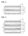
- the voltage nonlinear resistive element 10 includes the electrodes 16 and 18 on both sides of the resistor 14 containing one joined body 12, the resistor 14 may be replaced with a layered resistor composed of a plurality of joined bodies 12. Such a layered resistor can be used to control the varistor voltage. Thus, it is possible to manufacture a voltage nonlinear resistive element that has a varistor voltage suitable for the intended application. Examples that include a layered resistor are illustrated in Figs. 2 to 5 .
- a voltage nonlinear resistive element 30 illustrated in Fig. 2 includes a layered resistor 34 and electrodes 16 and 18 disposed on both sides of the layered resistor 34.
- the layered resistor 34 includes two joined bodies 12 stacked with a conductor layer 33 interposed therebetween.
- a rare-earth metal oxide layer 12b and the conductor layer 33 are disposed between adjacent zinc oxide ceramic layers 12a.
- the resistor 34 can be manufactured as described below. First, two joined bodies 12 are prepared.
- a zinc oxide ceramic layer 12a of one of the joined bodies 12 is brought into contact with a rare-earth metal oxide layer 12b of the other of the joined bodies 12 with a brazing filler (for example, Au-Ge alloy foil, Au-Sn alloy foil, or Au-Si alloy foil), which is a conductor foil, interposed therebetween.
- a brazing filler for example, Au-Ge alloy foil, Au-Sn alloy foil, or Au-Si alloy foil
- These are pressed into a single piece.
- the piece is heated at a predetermined joining temperature (for example, 300°C to 700°C, preferably 300°C to 500°C) in an inert atmosphere for a predetermined time and is then cooled. This allows the brazing filler to be melted or softened and then solidified and form the conductor layer 33, thus constituting the resistor 34.
- the voltage nonlinear resistive element 30 has the same advantages as the element 10. Because the layered resistor 34 includes the two joined bodies 12, the clamping voltage can be approximately twice the clamping voltage of the voltage nonlinear resistive element 10 according to Example 1. Furthermore, when the resistance of the zinc oxide ceramic layers 12a is decreased by adding a large amount of dopant (trivalent ion) to a zinc oxide ceramic or by forming a large number of oxygen deficiencies by heat treatment in an inert atmosphere, an excessively high joining temperature (for example, 900°C or 1000°C) sometimes results in high resistance due to precipitation of the dopant or elimination of the oxygen deficiencies. In this embodiment, however, because the joining temperature is 700°C or less, preferably 500°C or less, the zinc oxide ceramic layers 12a can have consistently low resistance.
- dopant trivalent ion
- a voltage nonlinear resistive element 130 illustrated in Fig. 3 includes a layered resistor 134 and electrodes 16 and 18 disposed on both sides of the layered resistor 134.
- the layered resistor 134 includes three joined bodies 12 stacked with a conductor layer 33 interposed therebetween. In the resistor 134, a rare-earth metal oxide layer 12b and the conductor layer 33 are disposed between adjacent zinc oxide ceramic layers 12a.
- the voltage nonlinear resistive element 130 has the same basic structure and advantages as the voltage nonlinear resistive element 30 illustrated in Fig. 2 and is therefore not described in detail. Because the layered resistor 134 in the element 130 includes the three joined bodies 12, the clamping voltage can be approximately three times the clamping voltage of the voltage nonlinear resistive element 10 according to Example 1.
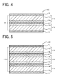
- a voltage nonlinear resistive element 40 illustrated in Fig. 4 includes a layered resistor 44 and electrodes 16 and 18 disposed on both sides of the layered resistor 44.
- the layered resistor 44 includes two joined bodies 12 stacked with a conductor layer 43 interposed therebetween.
- a rare-earth metal oxide layer 12b, the conductor layer 43, and another rare-earth metal oxide layer 12b are disposed between adjacent zinc oxide ceramic layers 12a.
- the resistor 44 can be manufactured as described below. First, two joined bodies 12 are prepared. A rare-earth metal oxide layer 12b of one of the joined bodies 12 is brought into contact with a rare-earth metal oxide layer 12b of the other of the joined bodies 12 with the brazing filler interposed therebetween.
- the voltage nonlinear resistive element 40 exhibits voltage nonlinearity.
- the clamping voltage of the voltage nonlinear resistive element 40 is almost the same as the clamping voltage of the voltage nonlinear resistive element 10 according to Example 1. Furthermore, for the reason described above for the voltage nonlinear resistive element 30, the zinc oxide ceramic layers 12a can have consistently low resistance.
- a voltage nonlinear resistive element 140 illustrated in Fig. 5 includes a layered resistor 144 and electrodes 16 and 18 disposed on both sides of the layered resistor 144.
- the layered resistor 144 includes two joined bodies 12 and one joined body 42 having a three-layer structure stacked with a conductor layer 43 interposed therebetween.
- a rare-earth metal oxide layer 12b, the conductor layer 43, and another rare-earth metal oxide layer 12b are disposed between adjacent zinc oxide ceramic layers 12a.
- the resistor 144 can be manufactured as described below. First, two joined bodies 12 are prepared.
- a zinc oxide ceramic layer 12a is overlaid with a rare-earth metal oxide layer 12b on both sides thereof, thereby producing the joined body 42 having the three-layer structure.
- a rare-earth metal oxide layer 12b of one of the joined bodies 12 is brought into contact with one of the rare-earth metal oxide layers 12b of the joined body 42 having the three-layer structure with the brazing filler interposed therebetween.
- the other of the rare-earth metal oxide layers 12b of the joined body 42 having the three-layer structure is brought into contact with a rare-earth metal oxide layer 12b of the other of the joined bodies 12 with the brazing filler interposed therebetween.
- the voltage nonlinear resistive element 140 In the same manner as in the voltage nonlinear resistive element 30, heat treatment in an inert atmosphere allows the brazing filler to be melted or softened and then solidified and form the conductor layer 43, thus constituting the resistor 144.
- a voltage is applied to the voltage nonlinear resistive element 140 such that the electrode 16 or the electrode 18 is an anode, the voltage nonlinear resistive element 140 exhibits voltage nonlinearity.
- the clamping voltage of the voltage nonlinear resistive element 140 is approximately twice the clamping voltage of the voltage nonlinear resistive element 10 according to Example 1.
- the joined bodies 12 may be directly joined without the brazing filler. Also in such a case, the joined bodies 12 are preferably joined at a relatively low temperature (for example, 300°C to 700°C, preferably 300°C to 500°C).
- Zinc oxide (average particle size 1.5 ⁇ m) was added to 0.1% by mass of ⁇ -alumina (average particle size 0.02 ⁇ m), the mixture was wet-blended, was dried, was passed through a sifter having a sieve opening of 75 ⁇ m, and was shaped to form a compact.
- the compact was degreased and held in a N 2 atmosphere at 1100°C for 5 hours and was then fired at 1400°C for 5 hours, thereby producing a zinc oxide ceramic block.
- the zinc oxide ceramic block had a volume resistivity of 9.0 x 10 -3 ⁇ cm.
- a 10 mm x 10 mm x 1 mm zinc oxide ceramic sheet was cut from the zinc oxide ceramic block.
- a sputtered praseodymium oxide film (thickness 0.3 ⁇ m) was formed on the zinc oxide ceramic sheet by high-frequency plasma sputtering a target of praseodymium oxide (Pr 2 O 3 ), thereby producing a joined body.
- RFS-200 manufactured by ULVAC KIKO, Inc. was used for sputtering.
- the deposition conditions were as follows: target size: 80 mm in diameter, RF output: 20 W, gas pressure (Ar): 2.0 Pa, deposition time: 15 minutes.
- the joined body was directly used as a resistor.
- An Al vapor deposition electrode was formed on both sides of the resistor.
- a voltage nonlinear resistive element was manufactured (see Fig. 1 ). Electric current-voltage characteristics were measured by applying a voltage between the electrodes of the voltage nonlinear resistive element.
- the electrode on the zinc oxide ceramic sheet was an anode, and the electrode on the praseodymium oxide sputtered film was a cathode.
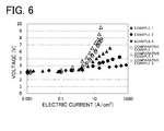
- Table 1 and Fig. 6 show the results.
- the clamping voltage at an electric current corresponding to 1 mA/cm 2 was 3.2 V
- the clamping voltage at an electric current corresponding to 20 A/cm 2 was 5.4 V.
- a zinc oxide ceramic block was produced in the same manner as in Example 1 except that zinc oxide was mixed with 1% by mass ⁇ -alumina.
- the zinc oxide ceramic block had a volume resistivity of 9.3 x 10 -4 ⁇ cm.
- a 10 mm x 10 mm x 1 mm zinc oxide ceramic sheet was cut from the zinc oxide ceramic block. The sheet is used to produce a joined body in the same manner as in Example 1. The joined body was directly used as a resistor. An Al vapor deposition electrode was formed on both sides of the resistor. Thus, a voltage nonlinear resistive element was manufactured. Electric current-voltage characteristics were measured by applying a voltage between the electrodes of the voltage nonlinear resistive element in the same manner as in Example 1. Table 1 and Fig. 6 show the results. The clamping voltage at an electric current corresponding to 1 mA/cm 2 was 3.1 V, and the clamping voltage at an electric current corresponding to 20 A/cm 2 was 4.4 V.
- a zinc oxide ceramic block was produced in the same manner as in Example 1 except that zinc oxide was mixed with 2% by mass ⁇ -alumina.
- the zinc oxide ceramic block had a volume resistivity of 1.1 x 10 -4 ⁇ cm.
- a 10 mm x 10 mm x 1 mm zinc oxide ceramic sheet was cut from the zinc oxide ceramic block. The sheet is used to produce a joined body in the same manner as in Example 1. The joined body was directly used as a resistor.
- An Al vapor deposition electrode was formed on both sides of the resistor.
- a voltage nonlinear resistive element was manufactured. Electric current-voltage characteristics were measured by applying a voltage between the electrodes of the voltage nonlinear resistive element in the same manner as in Example 1. Table 1 and Fig. 6 show the results.
- the clamping voltage at an electric current corresponding to 1 mA/cm 2 was 3.2 V
- the clamping voltage at an electric current corresponding to 20 A/cm 2 was 3.6 V.
- Aqueous aluminum nitrate was added to zinc oxide.
- the amount of aluminum nitrate was 0.01% by mass on an Al 2 O 3 basis.
- the water content of the product was adjusted to be 50% by mass by the addition of water.
- Minute amounts of binder and antifoaming agent were added to the product.
- the product was agitated by ultrasonic waves for 30 minutes and with an impeller blade for 30 minutes. After agitation, the product was granulated using a spray dryer to produce a granulated powder.
- the granulated powder was passed through a sifter having a sieve opening of 200 ⁇ m, was shaped, was degreased, and was fired in the air at 1400°C for 5 hours, thereby producing a zinc oxide ceramic block.
- the zinc oxide ceramic block had a volume resistivity of 2.0 x 10 -2 ⁇ cm.
- a 10 mm x 10 mm x 1 mm zinc oxide ceramic sheet was cut from the zinc oxide ceramic block.
- a sputtered rare-earth metal oxide film was formed on the zinc oxide ceramic sheet in the same manner as in Example 1, thereby producing a joined body.
- the joined body was directly used as a resistor.
- An Al vapor deposition electrode was formed on both sides of the resistor.
- a voltage nonlinear resistive element was manufactured. Electric current-voltage characteristics were measured by applying a voltage between the electrodes of the voltage nonlinear resistive element in the same manner as in Example 1.
- Table 1 and Fig. 6 show the results.
- the clamping voltage at an electric current corresponding to 1 mA/cm 2 was 2.9 V
- the clamping voltage at an electric current corresponding to 20 A/cm 2 was 7.3 V.
- Comparative Example 2 is an example in which a zinc oxide compact was fired in an air (in Example 1 and 2, the compact was fired in a N 2 atmosphere).
- Zinc oxide was added to 0.1% by mass of ⁇ -alumina, the mixture was wet-blended and dried. After heat-treating at a temperature of 1000°C, the calcined mixture was ground in a ball mill until the particle size of it becomes 1 ⁇ m or less.
- Zinc oxide and ⁇ -alumina are the same one as used in Example 1.
- the ground product was dried, was passed through a sifter having a sieve opening of 75 ⁇ m, and was shaped to form a compact.
- the compact was degreased and fired in an air at 1300°C for 5 hours, thereby producing a zinc oxide ceramic block.
- the zinc oxide ceramic block had a volume resistivity of 7.3 x 10 -1 ⁇ cm.
- a 10 mm x 10 mm x 1 mm zinc oxide ceramic sheet was cut from the zinc oxide ceramic block.
- a sputtered rare-earth metal oxide film (praseodymium oxide) was formed on the zinc oxide ceramic sheet in the same manner as in Example 1, thereby producing a joined body.
- the joined body was directly used as a resistor.
- An Al vapor deposition electrode was formed on both sides of the resistor.
- Electric current-voltage characteristics were measured by applying a voltage between the electrodes of the voltage nonlinear resistive element in the same manner as in Example 1.
- Table 1 and Fig. 6 show the results.
- the clamping voltage at an electric current corresponding to 1 mA/cm 2 was 3.3 V
- the clamping voltage at an electric current corresponding to 20 A/cm 2 was 8.5 V.
- a zinc oxide ceramic block was produced in the same manner as in Comparative Example 2 except that zinc oxide was mixed with 1% by mass ⁇ -alumina.
- the zinc oxide ceramic block had a volume resistivity of 3.5 x 10 -2 ⁇ cm.
- a 10 mm x 10 mm x 1 mm zinc oxide ceramic sheet was cut from the zinc oxide ceramic block.
- a sputtered rare-earth metal oxide film (praseodymium oxide) was formed on the zinc oxide ceramic sheet in the same manner as in Example 1, thereby producing a joined body.
- the joined body was directly used as a resistor.
- An Al vapor deposition electrode was formed on both sides of the resistor. Thus, a voltage nonlinear resistive element was manufactured.
- Electric current-voltage characteristics were measured by applying a voltage between the electrodes of the voltage nonlinear resistive element in the same manner as in Example 1.
- Table 1 and Fig. 6 show the results.
- the clamping voltage at an electric current corresponding to 1 mA/cm 2 was 2.9 V
- the clamping voltage at an electric current corresponding to 20 A/cm 2 was 7.4 V.
- Voltage generated in a high electric current region was lower in the voltage nonlinear resistive elements according to Examples 1 to 3, which included the zinc oxide ceramic sheet having a volume resistivity of less than 1.0 x 10 -2 ⁇ cm (particularly 1.0 x 10 -3 ⁇ cm or less), than in the voltage nonlinear resistive element according to Comparative Example 1 to 3, which included the zinc oxide ceramic sheet having a volume resistivity of 2.0 x 10 -2 ⁇ cm or more and being fired in an air.
- the voltage nonlinear resistive elements according to Examples 1 to 3 had an improved electronic circuit protective function.
- Two joined bodies were prepared in the same manner as in Example 3.
- the joined bodies in this state were joined by heat treatment in an inert atmosphere at 420°C for 10 minutes, thereby producing a layered resistor.
- An Al vapor deposition electrode was formed on both sides of the resistor.
- a voltage nonlinear resistive element was manufactured (see Fig. 2 ). Electric current-voltage characteristics were measured by applying a voltage between the electrodes of the voltage nonlinear resistive element.
- the electrode on the zinc oxide ceramic sheet was an anode, and the electrode on the sputtered film was a cathode.
- the voltage nonlinear resistive element had the voltage nonlinear resistance characteristics similar to that in Example 3.
- the clamping voltage in a nonlinearity region (a region having an electric current in the range of 0.01 to 2 A/cm 2 ) in this case was approximately twice the clamping voltage in Example 3.
- the voltage nonlinear resistive element of the present invention is applicable to elements for protecting electronic circuits from abnormal voltage, specifically used for various sensors, such as humidity sensors and temperature sensors.
Landscapes
- Engineering & Computer Science (AREA)
- Chemical & Material Sciences (AREA)
- Ceramic Engineering (AREA)
- Microelectronics & Electronic Packaging (AREA)
- Materials Engineering (AREA)
- Structural Engineering (AREA)
- Organic Chemistry (AREA)
- Manufacturing & Machinery (AREA)
- Physics & Mathematics (AREA)
- Electromagnetism (AREA)
- Inorganic Chemistry (AREA)
- Thermistors And Varistors (AREA)
- Compositions Of Oxide Ceramics (AREA)
- Non-Adjustable Resistors (AREA)
Applications Claiming Priority (1)
| Application Number | Priority Date | Filing Date | Title |
|---|---|---|---|
| JP2014056498 | 2014-03-19 |
Publications (3)
| Publication Number | Publication Date |
|---|---|
| EP2942789A2 true EP2942789A2 (de) | 2015-11-11 |
| EP2942789A3 EP2942789A3 (de) | 2016-01-27 |
| EP2942789B1 EP2942789B1 (de) | 2018-07-04 |
Family
ID=52684149
Family Applications (1)
| Application Number | Title | Priority Date | Filing Date |
|---|---|---|---|
| EP15159822.4A Active EP2942789B1 (de) | 2014-03-19 | 2015-03-19 | Nichtlineares resistives spannungselement und verfahren zur herstellung davon |
Country Status (6)
| Country | Link |
|---|---|
| US (1) | US9679685B2 (de) |
| EP (1) | EP2942789B1 (de) |
| JP (1) | JP6496582B2 (de) |
| KR (1) | KR20150109293A (de) |
| CN (1) | CN104934173A (de) |
| TW (1) | TW201606813A (de) |
Families Citing this family (4)
| Publication number | Priority date | Publication date | Assignee | Title |
|---|---|---|---|---|
| JP6496581B2 (ja) * | 2014-03-19 | 2019-04-03 | 日本碍子株式会社 | 電圧非直線抵抗素子及びその製法 |
| TW201606813A (zh) * | 2014-03-19 | 2016-02-16 | 日本碍子股份有限公司 | 電壓非線性電阻元件及其製法 |
| CN104794173A (zh) * | 2015-04-01 | 2015-07-22 | 惠州Tcl移动通信有限公司 | 一种基于移动终端的拍照处理方法及系统 |
| JP6703428B2 (ja) * | 2016-03-28 | 2020-06-03 | 日本碍子株式会社 | 電圧非直線抵抗素子及びその製法 |
Citations (1)
| Publication number | Priority date | Publication date | Assignee | Title |
|---|---|---|---|---|
| JP4123957B2 (ja) | 2003-02-10 | 2008-07-23 | 株式会社村田製作所 | 電圧依存性抵抗器 |
Family Cites Families (21)
| Publication number | Priority date | Publication date | Assignee | Title |
|---|---|---|---|---|
| GB764693A (en) * | 1954-01-06 | 1957-01-02 | E M P Electric Ltd | Improvements in non-linear resistor elements for lightning arresters |
| JPS5524247B2 (de) * | 1973-10-19 | 1980-06-27 | ||
| JPS5912002B2 (ja) * | 1979-05-10 | 1984-03-19 | 松下電器産業株式会社 | 電圧非直線抵抗器とその製造方法 |
| US4296002A (en) * | 1979-06-25 | 1981-10-20 | Mcgraw-Edison Company | Metal oxide varistor manufacture |
| US4272754A (en) * | 1979-12-17 | 1981-06-09 | General Electric Company | Thin film varistor |
| US4383237A (en) | 1980-05-07 | 1983-05-10 | Matsushita Electric Industrial Co., Ltd. | Voltage-dependent resistor |
| US4400683A (en) | 1981-09-18 | 1983-08-23 | Matsushita Electric Industrial Co., Ltd. | Voltage-dependent resistor |
| JPS5886702A (ja) * | 1981-11-19 | 1983-05-24 | 松下電器産業株式会社 | バリスタの製造方法 |
| JPH02214101A (ja) * | 1989-02-14 | 1990-08-27 | Tdk Corp | 電圧非直線性抵抗素子 |
| JPH06204006A (ja) * | 1992-10-20 | 1994-07-22 | Matsushita Electric Ind Co Ltd | 酸化亜鉛バリスタの製造方法 |
| JP2985559B2 (ja) * | 1993-03-17 | 1999-12-06 | 松下電器産業株式会社 | バリスタ |
| JP3622774B2 (ja) * | 1994-04-18 | 2005-02-23 | 株式会社村田製作所 | 電圧非直線抵抗体の製造方法 |
| US5854586A (en) * | 1997-09-17 | 1998-12-29 | Lockheed Martin Energy Research Corporation | Rare earth doped zinc oxide varistors |
| JP2000228302A (ja) * | 1999-02-04 | 2000-08-15 | Atsushi Iga | 酸化亜鉛系磁器積層物とその製造方法および酸化亜鉛バリスタ |
| JP2000243608A (ja) * | 1999-02-18 | 2000-09-08 | Atsushi Iga | 酸化亜鉛バリスタとその製造方法 |
| US6279811B1 (en) * | 2000-05-12 | 2001-08-28 | Mcgraw-Edison Company | Solder application technique |
| US8117739B2 (en) | 2004-01-23 | 2012-02-21 | Cooper Technologies Company | Manufacturing process for surge arrester module using pre-impregnated composite |
| JP5088029B2 (ja) * | 2007-07-19 | 2012-12-05 | Tdk株式会社 | バリスタ |
| DE102009023628A1 (de) * | 2009-05-27 | 2010-12-02 | Siemens Aktiengesellschaft | Verfahren zum Erzeugen einer Schicht mit Absorberpartikeln für eine Energiestrahlung |
| JP6496581B2 (ja) * | 2014-03-19 | 2019-04-03 | 日本碍子株式会社 | 電圧非直線抵抗素子及びその製法 |
| TW201606813A (zh) * | 2014-03-19 | 2016-02-16 | 日本碍子股份有限公司 | 電壓非線性電阻元件及其製法 |
-
2015
- 2015-03-19 TW TW104108730A patent/TW201606813A/zh unknown
- 2015-03-19 JP JP2015055491A patent/JP6496582B2/ja active Active
- 2015-03-19 KR KR1020150038098A patent/KR20150109293A/ko not_active Withdrawn
- 2015-03-19 CN CN201510121872.8A patent/CN104934173A/zh active Pending
- 2015-03-19 US US14/662,669 patent/US9679685B2/en active Active
- 2015-03-19 EP EP15159822.4A patent/EP2942789B1/de active Active
Patent Citations (1)
| Publication number | Priority date | Publication date | Assignee | Title |
|---|---|---|---|---|
| JP4123957B2 (ja) | 2003-02-10 | 2008-07-23 | 株式会社村田製作所 | 電圧依存性抵抗器 |
Also Published As
| Publication number | Publication date |
|---|---|
| JP6496582B2 (ja) | 2019-04-03 |
| EP2942789A3 (de) | 2016-01-27 |
| US20150270037A1 (en) | 2015-09-24 |
| KR20150109293A (ko) | 2015-10-01 |
| EP2942789B1 (de) | 2018-07-04 |
| JP2015195370A (ja) | 2015-11-05 |
| TW201606813A (zh) | 2016-02-16 |
| US9679685B2 (en) | 2017-06-13 |
| CN104934173A (zh) | 2015-09-23 |
Similar Documents
| Publication | Publication Date | Title |
|---|---|---|
| EP2942788B1 (de) | Nichtlineares resistives spannungselement und verfahren zur herstellung davon | |
| US7075404B2 (en) | Porcelain composition for varistor and varistor | |
| US9679685B2 (en) | Voltage nonlinear resistive element and method for manufacturing the same | |
| EP3196904A1 (de) | Keramische halbleiterelektronikkomponente in form eines chips | |
| KR101823770B1 (ko) | ZnO계 바리스터 조성물 및 그의 제조방법과 바리스터 | |
| EP3226261B1 (de) | Nichtlineares widerstandselement und verfahren zu seiner herstellung | |
| JP5830715B2 (ja) | 積層バリスタ及びその製造方法 | |
| JP4082696B2 (ja) | 積層型電子部品及びその製造方法 | |
| EP3202747B1 (de) | Bariumtitanathalbleiterkeramik, bariumtitanathalbleiterkeramikzusammensetzung und ptc-thermistor zur temperaturdetektion | |
| JP2013197447A (ja) | 積層バリスタの製造方法 | |
| CN100590756C (zh) | 可变电阻素体和可变电阻 | |
| JP7833647B2 (ja) | 積層バリスタ | |
| JP4292801B2 (ja) | 積層バリスタの製造方法 | |
| JP4087359B2 (ja) | 積層型チップバリスタ | |
| KR102666011B1 (ko) | ZnO계 바리스터 조성물과 이의 제조방법 및 바리스터 | |
| JP2009266976A (ja) | 酸化亜鉛積層チップバリスタの製造方法 | |
| JP2019165103A (ja) | 積層バリスタ | |
| JPH03261645A (ja) | バリスタ用磁器組成物 |
Legal Events
| Date | Code | Title | Description |
|---|---|---|---|
| PUAI | Public reference made under article 153(3) epc to a published international application that has entered the european phase |
Free format text: ORIGINAL CODE: 0009012 |
|
| AK | Designated contracting states |
Kind code of ref document: A2 Designated state(s): AL AT BE BG CH CY CZ DE DK EE ES FI FR GB GR HR HU IE IS IT LI LT LU LV MC MK MT NL NO PL PT RO RS SE SI SK SM TR |
|
| AX | Request for extension of the european patent |
Extension state: BA ME |
|
| PUAL | Search report despatched |
Free format text: ORIGINAL CODE: 0009013 |
|
| AK | Designated contracting states |
Kind code of ref document: A3 Designated state(s): AL AT BE BG CH CY CZ DE DK EE ES FI FR GB GR HR HU IE IS IT LI LT LU LV MC MK MT NL NO PL PT RO RS SE SI SK SM TR |
|
| AX | Request for extension of the european patent |
Extension state: BA ME |
|
| RIC1 | Information provided on ipc code assigned before grant |
Ipc: H01C 7/112 20060101ALI20151223BHEP Ipc: H01C 7/18 20060101ALI20151223BHEP Ipc: H01C 7/102 20060101AFI20151223BHEP Ipc: H01C 7/12 20060101ALI20151223BHEP Ipc: C01G 9/02 20060101ALI20151223BHEP Ipc: C04B 35/453 20060101ALI20151223BHEP Ipc: H01C 7/10 20060101ALN20151223BHEP |
|
| 17P | Request for examination filed |
Effective date: 20160726 |
|
| RBV | Designated contracting states (corrected) |
Designated state(s): AL AT BE BG CH CY CZ DE DK EE ES FI FR GB GR HR HU IE IS IT LI LT LU LV MC MK MT NL NO PL PT RO RS SE SI SK SM TR |
|
| RIC1 | Information provided on ipc code assigned before grant |
Ipc: C04B 35/626 20060101ALI20171130BHEP Ipc: H01C 7/12 20060101ALI20171130BHEP Ipc: H01C 7/18 20060101ALI20171130BHEP Ipc: H01C 7/102 20060101AFI20171130BHEP Ipc: C01G 9/02 20060101ALI20171130BHEP Ipc: H01C 7/10 20060101ALN20171130BHEP Ipc: C04B 37/00 20060101ALI20171130BHEP Ipc: C04B 35/453 20060101ALI20171130BHEP Ipc: H01C 7/112 20060101ALI20171130BHEP |
|
| GRAP | Despatch of communication of intention to grant a patent |
Free format text: ORIGINAL CODE: EPIDOSNIGR1 |
|
| STAA | Information on the status of an ep patent application or granted ep patent |
Free format text: STATUS: GRANT OF PATENT IS INTENDED |
|
| RIC1 | Information provided on ipc code assigned before grant |
Ipc: C01G 9/02 20060101ALI20171206BHEP Ipc: H01C 7/12 20060101ALI20171206BHEP Ipc: C04B 35/626 20060101ALI20171206BHEP Ipc: H01C 7/10 20060101ALN20171206BHEP Ipc: C04B 35/453 20060101ALI20171206BHEP Ipc: H01C 7/18 20060101ALI20171206BHEP Ipc: H01C 7/112 20060101ALI20171206BHEP Ipc: C04B 37/00 20060101ALI20171206BHEP Ipc: H01C 7/102 20060101AFI20171206BHEP |
|
| INTG | Intention to grant announced |
Effective date: 20180108 |
|
| RIN1 | Information on inventor provided before grant (corrected) |
Inventor name: TAKEUCHI, YUKIHISA Inventor name: HAYASE, TORU Inventor name: MORIMOTO, KENJI Inventor name: KAWASAKI, SHINJI Inventor name: YAMAKAZI, SATOSHI |
|
| GRAJ | Information related to disapproval of communication of intention to grant by the applicant or resumption of examination proceedings by the epo deleted |
Free format text: ORIGINAL CODE: EPIDOSDIGR1 |
|
| STAA | Information on the status of an ep patent application or granted ep patent |
Free format text: STATUS: REQUEST FOR EXAMINATION WAS MADE |
|
| GRAR | Information related to intention to grant a patent recorded |
Free format text: ORIGINAL CODE: EPIDOSNIGR71 |
|
| GRAS | Grant fee paid |
Free format text: ORIGINAL CODE: EPIDOSNIGR3 |
|
| STAA | Information on the status of an ep patent application or granted ep patent |
Free format text: STATUS: GRANT OF PATENT IS INTENDED |
|
| GRAA | (expected) grant |
Free format text: ORIGINAL CODE: 0009210 |
|
| STAA | Information on the status of an ep patent application or granted ep patent |
Free format text: STATUS: THE PATENT HAS BEEN GRANTED |
|
| INTC | Intention to grant announced (deleted) | ||
| RIC1 | Information provided on ipc code assigned before grant |
Ipc: H01C 7/12 20060101ALI20180518BHEP Ipc: C04B 37/00 20060101ALI20180518BHEP Ipc: C01G 9/02 20060101ALI20180518BHEP Ipc: H01C 7/18 20060101ALI20180518BHEP Ipc: H01C 7/102 20060101AFI20180518BHEP Ipc: H01C 7/10 20060101ALN20180518BHEP Ipc: C04B 35/453 20060101ALI20180518BHEP Ipc: H01C 7/112 20060101ALI20180518BHEP Ipc: C04B 35/626 20060101ALI20180518BHEP |
|
| AK | Designated contracting states |
Kind code of ref document: B1 Designated state(s): AL AT BE BG CH CY CZ DE DK EE ES FI FR GB GR HR HU IE IS IT LI LT LU LV MC MK MT NL NO PL PT RO RS SE SI SK SM TR |
|
| INTG | Intention to grant announced |
Effective date: 20180525 |
|
| REG | Reference to a national code |
Ref country code: GB Ref legal event code: FG4D |
|
| REG | Reference to a national code |
Ref country code: CH Ref legal event code: EP |
|
| REG | Reference to a national code |
Ref country code: AT Ref legal event code: REF Ref document number: 1015387 Country of ref document: AT Kind code of ref document: T Effective date: 20180715 |
|
| REG | Reference to a national code |
Ref country code: IE Ref legal event code: FG4D |
|
| REG | Reference to a national code |
Ref country code: DE Ref legal event code: R096 Ref document number: 602015012884 Country of ref document: DE |
|
| REG | Reference to a national code |
Ref country code: NL Ref legal event code: MP Effective date: 20180704 |
|
| REG | Reference to a national code |
Ref country code: LT Ref legal event code: MG4D |
|
| REG | Reference to a national code |
Ref country code: AT Ref legal event code: MK05 Ref document number: 1015387 Country of ref document: AT Kind code of ref document: T Effective date: 20180704 |
|
| PG25 | Lapsed in a contracting state [announced via postgrant information from national office to epo] |
Ref country code: NL Free format text: LAPSE BECAUSE OF FAILURE TO SUBMIT A TRANSLATION OF THE DESCRIPTION OR TO PAY THE FEE WITHIN THE PRESCRIBED TIME-LIMIT Effective date: 20180704 |
|
| PG25 | Lapsed in a contracting state [announced via postgrant information from national office to epo] |
Ref country code: FI Free format text: LAPSE BECAUSE OF FAILURE TO SUBMIT A TRANSLATION OF THE DESCRIPTION OR TO PAY THE FEE WITHIN THE PRESCRIBED TIME-LIMIT Effective date: 20180704 Ref country code: CZ Free format text: LAPSE BECAUSE OF FAILURE TO SUBMIT A TRANSLATION OF THE DESCRIPTION OR TO PAY THE FEE WITHIN THE PRESCRIBED TIME-LIMIT Effective date: 20180704 Ref country code: LT Free format text: LAPSE BECAUSE OF FAILURE TO SUBMIT A TRANSLATION OF THE DESCRIPTION OR TO PAY THE FEE WITHIN THE PRESCRIBED TIME-LIMIT Effective date: 20180704 Ref country code: PL Free format text: LAPSE BECAUSE OF FAILURE TO SUBMIT A TRANSLATION OF THE DESCRIPTION OR TO PAY THE FEE WITHIN THE PRESCRIBED TIME-LIMIT Effective date: 20180704 Ref country code: NO Free format text: LAPSE BECAUSE OF FAILURE TO SUBMIT A TRANSLATION OF THE DESCRIPTION OR TO PAY THE FEE WITHIN THE PRESCRIBED TIME-LIMIT Effective date: 20181004 Ref country code: BG Free format text: LAPSE BECAUSE OF FAILURE TO SUBMIT A TRANSLATION OF THE DESCRIPTION OR TO PAY THE FEE WITHIN THE PRESCRIBED TIME-LIMIT Effective date: 20181004 Ref country code: AT Free format text: LAPSE BECAUSE OF FAILURE TO SUBMIT A TRANSLATION OF THE DESCRIPTION OR TO PAY THE FEE WITHIN THE PRESCRIBED TIME-LIMIT Effective date: 20180704 Ref country code: SE Free format text: LAPSE BECAUSE OF FAILURE TO SUBMIT A TRANSLATION OF THE DESCRIPTION OR TO PAY THE FEE WITHIN THE PRESCRIBED TIME-LIMIT Effective date: 20180704 Ref country code: IS Free format text: LAPSE BECAUSE OF FAILURE TO SUBMIT A TRANSLATION OF THE DESCRIPTION OR TO PAY THE FEE WITHIN THE PRESCRIBED TIME-LIMIT Effective date: 20181104 Ref country code: RS Free format text: LAPSE BECAUSE OF FAILURE TO SUBMIT A TRANSLATION OF THE DESCRIPTION OR TO PAY THE FEE WITHIN THE PRESCRIBED TIME-LIMIT Effective date: 20180704 Ref country code: GR Free format text: LAPSE BECAUSE OF FAILURE TO SUBMIT A TRANSLATION OF THE DESCRIPTION OR TO PAY THE FEE WITHIN THE PRESCRIBED TIME-LIMIT Effective date: 20181005 |
|
| PG25 | Lapsed in a contracting state [announced via postgrant information from national office to epo] |
Ref country code: ES Free format text: LAPSE BECAUSE OF FAILURE TO SUBMIT A TRANSLATION OF THE DESCRIPTION OR TO PAY THE FEE WITHIN THE PRESCRIBED TIME-LIMIT Effective date: 20180704 Ref country code: HR Free format text: LAPSE BECAUSE OF FAILURE TO SUBMIT A TRANSLATION OF THE DESCRIPTION OR TO PAY THE FEE WITHIN THE PRESCRIBED TIME-LIMIT Effective date: 20180704 Ref country code: AL Free format text: LAPSE BECAUSE OF FAILURE TO SUBMIT A TRANSLATION OF THE DESCRIPTION OR TO PAY THE FEE WITHIN THE PRESCRIBED TIME-LIMIT Effective date: 20180704 Ref country code: LV Free format text: LAPSE BECAUSE OF FAILURE TO SUBMIT A TRANSLATION OF THE DESCRIPTION OR TO PAY THE FEE WITHIN THE PRESCRIBED TIME-LIMIT Effective date: 20180704 |
|
| REG | Reference to a national code |
Ref country code: DE Ref legal event code: R097 Ref document number: 602015012884 Country of ref document: DE |
|
| PG25 | Lapsed in a contracting state [announced via postgrant information from national office to epo] |
Ref country code: EE Free format text: LAPSE BECAUSE OF FAILURE TO SUBMIT A TRANSLATION OF THE DESCRIPTION OR TO PAY THE FEE WITHIN THE PRESCRIBED TIME-LIMIT Effective date: 20180704 Ref country code: IT Free format text: LAPSE BECAUSE OF FAILURE TO SUBMIT A TRANSLATION OF THE DESCRIPTION OR TO PAY THE FEE WITHIN THE PRESCRIBED TIME-LIMIT Effective date: 20180704 Ref country code: RO Free format text: LAPSE BECAUSE OF FAILURE TO SUBMIT A TRANSLATION OF THE DESCRIPTION OR TO PAY THE FEE WITHIN THE PRESCRIBED TIME-LIMIT Effective date: 20180704 |
|
| PLBE | No opposition filed within time limit |
Free format text: ORIGINAL CODE: 0009261 |
|
| STAA | Information on the status of an ep patent application or granted ep patent |
Free format text: STATUS: NO OPPOSITION FILED WITHIN TIME LIMIT |
|
| PG25 | Lapsed in a contracting state [announced via postgrant information from national office to epo] |
Ref country code: DK Free format text: LAPSE BECAUSE OF FAILURE TO SUBMIT A TRANSLATION OF THE DESCRIPTION OR TO PAY THE FEE WITHIN THE PRESCRIBED TIME-LIMIT Effective date: 20180704 Ref country code: SK Free format text: LAPSE BECAUSE OF FAILURE TO SUBMIT A TRANSLATION OF THE DESCRIPTION OR TO PAY THE FEE WITHIN THE PRESCRIBED TIME-LIMIT Effective date: 20180704 Ref country code: SM Free format text: LAPSE BECAUSE OF FAILURE TO SUBMIT A TRANSLATION OF THE DESCRIPTION OR TO PAY THE FEE WITHIN THE PRESCRIBED TIME-LIMIT Effective date: 20180704 |
|
| 26N | No opposition filed |
Effective date: 20190405 |
|
| PG25 | Lapsed in a contracting state [announced via postgrant information from national office to epo] |
Ref country code: SI Free format text: LAPSE BECAUSE OF FAILURE TO SUBMIT A TRANSLATION OF THE DESCRIPTION OR TO PAY THE FEE WITHIN THE PRESCRIBED TIME-LIMIT Effective date: 20180704 |
|
| PG25 | Lapsed in a contracting state [announced via postgrant information from national office to epo] |
Ref country code: MC Free format text: LAPSE BECAUSE OF FAILURE TO SUBMIT A TRANSLATION OF THE DESCRIPTION OR TO PAY THE FEE WITHIN THE PRESCRIBED TIME-LIMIT Effective date: 20180704 |
|
| REG | Reference to a national code |
Ref country code: CH Ref legal event code: PL |
|
| GBPC | Gb: european patent ceased through non-payment of renewal fee |
Effective date: 20190319 |
|
| PG25 | Lapsed in a contracting state [announced via postgrant information from national office to epo] |
Ref country code: LU Free format text: LAPSE BECAUSE OF NON-PAYMENT OF DUE FEES Effective date: 20190319 |
|
| REG | Reference to a national code |
Ref country code: BE Ref legal event code: MM Effective date: 20190331 |
|
| PG25 | Lapsed in a contracting state [announced via postgrant information from national office to epo] |
Ref country code: IE Free format text: LAPSE BECAUSE OF NON-PAYMENT OF DUE FEES Effective date: 20190319 Ref country code: GB Free format text: LAPSE BECAUSE OF NON-PAYMENT OF DUE FEES Effective date: 20190319 Ref country code: CH Free format text: LAPSE BECAUSE OF NON-PAYMENT OF DUE FEES Effective date: 20190331 Ref country code: LI Free format text: LAPSE BECAUSE OF NON-PAYMENT OF DUE FEES Effective date: 20190331 |
|
| PG25 | Lapsed in a contracting state [announced via postgrant information from national office to epo] |
Ref country code: BE Free format text: LAPSE BECAUSE OF NON-PAYMENT OF DUE FEES Effective date: 20190331 |
|
| PG25 | Lapsed in a contracting state [announced via postgrant information from national office to epo] |
Ref country code: TR Free format text: LAPSE BECAUSE OF FAILURE TO SUBMIT A TRANSLATION OF THE DESCRIPTION OR TO PAY THE FEE WITHIN THE PRESCRIBED TIME-LIMIT Effective date: 20180704 |
|
| PG25 | Lapsed in a contracting state [announced via postgrant information from national office to epo] |
Ref country code: MT Free format text: LAPSE BECAUSE OF NON-PAYMENT OF DUE FEES Effective date: 20190319 Ref country code: PT Free format text: LAPSE BECAUSE OF FAILURE TO SUBMIT A TRANSLATION OF THE DESCRIPTION OR TO PAY THE FEE WITHIN THE PRESCRIBED TIME-LIMIT Effective date: 20181104 |
|
| PG25 | Lapsed in a contracting state [announced via postgrant information from national office to epo] |
Ref country code: CY Free format text: LAPSE BECAUSE OF FAILURE TO SUBMIT A TRANSLATION OF THE DESCRIPTION OR TO PAY THE FEE WITHIN THE PRESCRIBED TIME-LIMIT Effective date: 20180704 |
|
| PG25 | Lapsed in a contracting state [announced via postgrant information from national office to epo] |
Ref country code: HU Free format text: LAPSE BECAUSE OF FAILURE TO SUBMIT A TRANSLATION OF THE DESCRIPTION OR TO PAY THE FEE WITHIN THE PRESCRIBED TIME-LIMIT; INVALID AB INITIO Effective date: 20150319 |
|
| PG25 | Lapsed in a contracting state [announced via postgrant information from national office to epo] |
Ref country code: MK Free format text: LAPSE BECAUSE OF FAILURE TO SUBMIT A TRANSLATION OF THE DESCRIPTION OR TO PAY THE FEE WITHIN THE PRESCRIBED TIME-LIMIT Effective date: 20180704 |
|
| PGFP | Annual fee paid to national office [announced via postgrant information from national office to epo] |
Ref country code: DE Payment date: 20260128 Year of fee payment: 12 |
|
| PGFP | Annual fee paid to national office [announced via postgrant information from national office to epo] |
Ref country code: FR Payment date: 20260209 Year of fee payment: 12 |