EP2904641B1 - Wasserstoffabschwächungsschemata bei der passivierung fortgeschrittener vorrichtungen - Google Patents
Wasserstoffabschwächungsschemata bei der passivierung fortgeschrittener vorrichtungen Download PDFInfo
- Publication number
- EP2904641B1 EP2904641B1 EP13774322.5A EP13774322A EP2904641B1 EP 2904641 B1 EP2904641 B1 EP 2904641B1 EP 13774322 A EP13774322 A EP 13774322A EP 2904641 B1 EP2904641 B1 EP 2904641B1
- Authority
- EP
- European Patent Office
- Prior art keywords
- hydrogen
- semiconductor body
- silicon nitride
- layer
- contact
- Prior art date
- Legal status (The legal status is an assumption and is not a legal conclusion. Google has not performed a legal analysis and makes no representation as to the accuracy of the status listed.)
- Active
Links
Images


Classifications
-
- H—ELECTRICITY
- H10—SEMICONDUCTOR DEVICES; ELECTRIC SOLID-STATE DEVICES NOT OTHERWISE PROVIDED FOR
- H10D—INORGANIC ELECTRIC SEMICONDUCTOR DEVICES
- H10D30/00—Field-effect transistors [FET]
- H10D30/40—FETs having zero-dimensional [0D], one-dimensional [1D] or two-dimensional [2D] charge carrier gas channels
- H10D30/47—FETs having zero-dimensional [0D], one-dimensional [1D] or two-dimensional [2D] charge carrier gas channels having two-dimensional [2D] charge carrier gas channels, e.g. nanoribbon FETs or high electron mobility transistors [HEMT]
- H10D30/471—High electron mobility transistors [HEMT] or high hole mobility transistors [HHMT]
- H10D30/475—High electron mobility transistors [HEMT] or high hole mobility transistors [HHMT] having wider bandgap layer formed on top of lower bandgap active layer, e.g. undoped barrier HEMTs such as i-AlGaN/GaN HEMTs
- H10D30/4755—High electron mobility transistors [HEMT] or high hole mobility transistors [HHMT] having wider bandgap layer formed on top of lower bandgap active layer, e.g. undoped barrier HEMTs such as i-AlGaN/GaN HEMTs having wide bandgap charge-carrier supplying layers, e.g. modulation doped HEMTs such as n-AlGaAs/GaAs HEMTs
-
- H—ELECTRICITY
- H10—SEMICONDUCTOR DEVICES; ELECTRIC SOLID-STATE DEVICES NOT OTHERWISE PROVIDED FOR
- H10D—INORGANIC ELECTRIC SEMICONDUCTOR DEVICES
- H10D30/00—Field-effect transistors [FET]
- H10D30/01—Manufacture or treatment
- H10D30/015—Manufacture or treatment of FETs having heterojunction interface channels or heterojunction gate electrodes, e.g. HEMT
-
- H—ELECTRICITY
- H10—SEMICONDUCTOR DEVICES; ELECTRIC SOLID-STATE DEVICES NOT OTHERWISE PROVIDED FOR
- H10W—GENERIC PACKAGES, INTERCONNECTIONS, CONNECTORS OR OTHER CONSTRUCTIONAL DETAILS OF DEVICES COVERED BY CLASS H10
- H10W74/00—Encapsulations, e.g. protective coatings
- H10W74/40—Encapsulations, e.g. protective coatings characterised by their materials
- H10W74/43—Encapsulations, e.g. protective coatings characterised by their materials comprising oxides, nitrides or carbides, e.g. ceramics or glasses
-
- H—ELECTRICITY
- H10—SEMICONDUCTOR DEVICES; ELECTRIC SOLID-STATE DEVICES NOT OTHERWISE PROVIDED FOR
- H10D—INORGANIC ELECTRIC SEMICONDUCTOR DEVICES
- H10D62/00—Semiconductor bodies, or regions thereof, of devices having potential barriers
- H10D62/80—Semiconductor bodies, or regions thereof, of devices having potential barriers characterised by the materials
- H10D62/85—Semiconductor bodies, or regions thereof, of devices having potential barriers characterised by the materials being Group III-V materials, e.g. GaAs
- H10D62/8503—Nitride Group III-V materials, e.g. AlN or GaN
-
- H—ELECTRICITY
- H10—SEMICONDUCTOR DEVICES; ELECTRIC SOLID-STATE DEVICES NOT OTHERWISE PROVIDED FOR
- H10W—GENERIC PACKAGES, INTERCONNECTIONS, CONNECTORS OR OTHER CONSTRUCTIONAL DETAILS OF DEVICES COVERED BY CLASS H10
- H10W74/00—Encapsulations, e.g. protective coatings
- H10W74/10—Encapsulations, e.g. protective coatings characterised by their shape or disposition
- H10W74/131—Encapsulations, e.g. protective coatings characterised by their shape or disposition the semiconductor body being only partially enclosed
- H10W74/137—Encapsulations, e.g. protective coatings characterised by their shape or disposition the semiconductor body being only partially enclosed the encapsulations being directly on the semiconductor body
Definitions
- the present disclosure relates to passivation of a semiconductor device.
- SiN Chemical Vapor Deposition
- SiN Silicon Nitride
- MESFETs Metal Semiconductor Field Effect Transistors
- MOSFETs Metal Oxide Semiconductor Field Effect Transistors
- CVD SiN has relatively low permittivity, good encapsulation properties, and is easy to deposit.
- Hydrogen present in CVD SiN passivation structures adversely affects device characteristics. As such, there is a need for a SiN passivation structure that eliminates or substantially reduces the effects of Hydrogen in the SiN passivation structure.
- WO2011/125928 discloses a semiconductor device comprising: an interlayer insulating film; a wiring line that is formed on the interlayer insulating film so as to protrude therefrom; and a passivation film that is formed so as to cover the wiring line.
- the passivation film is composed of a laminated film wherein a first nitride film, an intermediate film and a second nitride film are laminated in this order from the wiring line side.
- the intermediate film is formed of an insulating material (for example, an oxide) that is different from those of the first and second nitride films.
- US2008/035934 discloses a field effect transistor formed in the Group III nitride material system including a two-part structure in which a chemical vapor deposited passivation layer of silicon nitride encapsulates a previously sputtered-deposited layer of silicon nitride.
- US2007/001174 discloses a passivated semiconductor structure including a silicon carbide substrate; an oxidation layer on the silicon carbide substrate; a first sputtered non-stoichiometric silicon nitride layer on the thermal oxidation layer; a second sputtered non-stoichiometric silicon nitride layer on the first layer; a sputtered stoichiometric silicon nitride layer on the second sputtered layer; and a chemical vapor deposited environmental barrier layer of stoichiometric silicon nitride.
- US6611014 discloses a semiconductor device having a semiconductor substrate; an insulating film formed on said semiconductor substrate; a ferroelectric capacitor having a lower electrode, a ferroelectric film and an upper electrode which are stacked sequentially on the insulating film; a first hydrogen barrier film; a first inter-layer insulating film covering said ferroelectric capacitor; and a second inter-layer insulating film stacked on the first inter-layer insulating film, the first hydrogen barrier film being interposed between the first and second interlayer insulating films is proposed.
- US2007/164321 discloses transistors having a protective layer with an opening extending therethrough on a substrate, and a gate electrode in the opening.
- Embodiments of a Silicon Nitride (SiN) passivation structure for a semiconductor device and methods of fabrication thereof are disclosed.
- the semiconductor device may be, for example, a Metal Semiconductor Field Effect Transistor (MESFET), a High Electron Mobility Transistor (HEMT), a Metal Oxide Semiconductor Field Effect Transistors (MOSFET), or the like.
- a semiconductor device includes a semiconductor body and a SiN passivation structure over a surface of the semiconductor body.
- the SiN passivation structure includes one or more Hydrogen-free SiN layers on, and preferably directly on, the surface of the semiconductor body, a Hydrogen barrier layer on, and preferably directly on, a surface of the one or more Hydrogen-free SiN layers opposite the semiconductor body, and a Chemical Vapor Deposition (CVD) SiN layer on, and preferably directly on, a surface of the Hydrogen barrier layer opposite the one or more Hydrogen-free SiN layers.
- the CVD SiN layer is preferably a Plasma Enhanced CVD (PECVD) SiN layer.
- the Hydrogen barrier layer includes a repeating sequence of different oxide layers.
- the Hydrogen barrier layer includes stoichiometric monolayers of different compositions formed by Atomic Layer Deposition (ALD).
- the one or more Hydrogen-free SiN layers include a first Hydrogen-free SiN layer on, and preferably directly on, the surface of the semiconductor body and a second Hydrogen-free SiN layer on, and preferably directly on, a surface of the first Hydrogen-free SiN layer opposite the semiconductor body.
- a refractive index of the first Hydrogen-free SiN layer is in a range of and including 1.84 to 1.95 and, in one preferred embodiment, is approximately equal to 1.86 (e.g., 1.86 ⁇ 10%, 1.86 ⁇ 5%, or 1.86 ⁇ 1%), and a refractive index of the second Hydrogen-free SiN layer is in a range of and including 1.95 to 2.03 and, in one preferred embodiment, is approximately equal to 2.02 (e.g., 2.02 ⁇ 10%, 2.02 ⁇ 5%, or 2.02 ⁇ 1%).
- the first and second Hydrogen-free SiN layers are sputter-deposited SiN layers.
- CVD SiN Chemical Vapor Deposition
- SiN Silicon Nitride
- MESFETs Metal Semiconductor Field Effect Transistors
- HEMTs High Electron Mobility Transistors
- MOSFETs Metal Oxide Semiconductor Field Effect Transistors
- CVD SiN has relatively low permittivity, good encapsulation properties, and is easy to deposit.
- the inventors have found that one issue with CVD SiN passivation is that the CVD SiN contains a significant amount of Hydrogen stemming from the use of ammonia and silane as the precursors for the CVD process.
- This Hydrogen is weakly bonded in the SiN and, as such, can become mobile at elevated temperatures, which wreaks havoc on device performance. Specifically, as the Hydrogen becomes mobile, the Hydrogen represents mobile charges and can be re-trapped in different device areas, thereby changing device characteristics. As such, there is a need for a SiN passivation structure that eliminates or substantially reduces the effects of Hydrogen in the SiN passivation structure.
- FIG. 1 illustrates a semiconductor device, and in particular a Metal Semiconductor Field Effect Transistor (MESFET) 10, that incorporates a SiN passivation structure 12 according to one embodiment of the present disclosure.
- the SiN passivation structure 12 is not limited to use with the MESFET 10. Rather, the SiN passivation structure 12 can be utilized for passivation of any suitable semiconductor device.
- additional semiconductor devices with which the SiN passivation structure 12 can be used are described below. However, these additional examples are only examples and are not to be construed as an exhaustive list of semiconductor devices with which the SiN passivation structure 12 can be used.
- the MESFET 10 includes a substrate 14 and a semiconductor body 16 on a surface of the substrate 14.
- the substrate 14 is preferably formed of Silicon Carbide (SiC), but is not limited thereto.
- the substrate 14 may be formed of other materials such as, for example, Sapphire, Aluminum Nitride (AIN), Aluminum Gallium Nitride (AIGaN), Gallium Nitride (GaN), Silicon (Si), Gallium Arsenide (GaAs), Zinc Oxide (ZnO), and Indium Phosphide (InP).
- the semiconductor body 16 preferably includes one or more epitaxial layers of one or more wideband materials such as, for example, one or more Group III nitrides.
- the semiconductor body 16 may be formed of one or more layers of GaN or AIGaN. However, other Group III nitride materials may be used.
- a source region 18 and a drain region 20 are formed in the semiconductor body 16 by, for example, implanting appropriate ions into a surface of the semiconductor body 16 to achieve a desired doping concentration.
- a source contact 22 is formed by one or more metallic layers on, and preferably directly on, the surface of the semiconductor body 16 adjacent to the source region 18.
- a drain contact 24 is formed by one or more metallic layers on, and preferably directly on, the surface of the semiconductor body 16 adjacent to the drain region 20.
- the source and drain contacts 22 and 24 preferably provide low-resistance ohmic contacts to the source and drain regions 18 and 20, respectively.
- a gate contact 26 is formed by one or more metallic layers on, and preferably directly on, a surface of the semiconductor body 16 between the source region 18 and the drain region 20.
- the region within the semiconductor body 16 between the source and drain regions 18 and 20 is a channel region of the MESFET 10.
- the SiN passivation structure 12 is formed on the surface of the semiconductor body 16 between the source contact 22 and the gate contact 26 and between the drain contact 24 and the gate contact 26. In this embodiment, the SiN passivation structure 12 extends over the gate contact 26. As discussed below, the SiN passivation structure 12 eliminates or at least mitigates the effects of Hydrogen in the SiN passivation structure 12 on the performance of the MESFET 10.
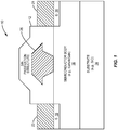
- Figure 2 illustrates the SiN passivation structure 12 of Figure 1 in more detail according to one embodiment of the present disclosure.
- the SiN passivation structure 12 includes a Hydrogen-free SiN layer 28 on, and preferably directly on, the surface of the semiconductor body 16 opposite the substrate 14.
- the Hydrogen-free SiN layer 28 is etched to form an opening in which the gate contact 26 is formed such that the gate contact 26 is in contact with the semiconductor body 16.
- the SiN passivation structure 12 also includes a Hydrogen-free SiN layer 30 on, and preferably directly on, a surface of the Hydrogen-free SiN layer 28 and a surface of the gate contact 26 opposite the semiconductor body 16.
- the Hydrogen-free SiN layers 28 and 30 form a first passivation substructure that provides some benefits of SiN passivation (e.g., reduces parasitic capacitance, minimizes device trapping) and, in addition, positions subsequent passivation layers further from the channel region.
- the SiN passivation structure 12 includes a Hydrogen barrier layer 32 on, and preferably directly on, a surface of the Hydrogen-free SiN layer 30 opposite the Hydrogen-free SiN layer 28.
- the Hydrogen barrier layer 32 includes more than one oxide layer of different composition.
- the Hydrogen barrier layer 32 includes layers of SiO 2 , Aluminum Oxide (Al 2 O 3 ), Titanium (III) Oxide (TiO), Hafnium Oxide (HfO), and/or the like.
- the Hydrogen barrier layer 32 includes one or more repeating sequences of oxide layers (e.g., SiO 2 , Al 2 O 3 , SiO 2 , Al 2 O 3 , etc.).
- the Hydrogen barrier layer 32 is preferably stoichiometric monolayers of different compositions formed by Atomic Layer Deposition (ALD).
- the SiN passivation structure 12 includes a Chemical Vapor Deposition (CVD) SiN layer 34 on, and preferably directly on, a surface of the Hydrogen barrier layer 32 opposite the Hydrogen-free SiN layer 30.
- the CVD SiN layer 34 is formed by Plasma Enhanced Chemical Vapor Deposition (PECVD) using ammonia and silane as precursors.
- PECVD Plasma Enhanced Chemical Vapor Deposition
- the CVD SiN layer 34 includes a substantial amount of Hydrogen.
- the Hydrogen barrier layer 32 along with the Hydrogen barrier properties of the Hydrogen-free SiN layers 28 and 30 prevent, or at least substantially reduce, migration of Hydrogen toward the surface of the semiconductor body 16.
- the CVD SiN layer 34 is replaced with a SiN layer formed via ALD where the ALD process may, in some embodiments, use precursors that reduce or substantially eliminate Hydrogen in the SiN layer as compared to the CVD SiN layer 34.
- a "Hydrogen-free" layer is a layer that has no Hydrogen or no substantial amount of Hydrogen.
- sputtering is one technique that may be used to form a Hydrogen-free SiN layer.
- the Hydrogen-free SiN layers 28 and 30 are sputter-deposited SiN layers (i.e., SiN layers formed using a sputtering technique(s)).
- a PECVD SiN layer formed using ammonia and silane as precursors includes a substantial amount of Hydrogen (e.g., about 15% to 22% Hydrogen) and is therefore not Hydrogen-free.
- a sputtered layer of SiN has substantially no Hydrogen as compared to that contained in a PECVD SiN layer because, unlike PECVD which is a chemical process, sputtering SiN is a reactive physical process where Silicon atoms are knocked off of the target in the presence of Nitrogen gas flow under pressure and bias. So, for sputtered SiN, the only Hydrogen present in the SiN is incorporated from the walls of the growth chamber or the surface of the wafer after loading the wafer into the growth chamber.
- the proportion of Silicon or Nitrogen in SiN can be determined by the refractive index of the SiN.
- the refractive index is an indicator of the composition of a SiN film.
- a refractive index of the Hydrogen-free SiN layer 28 is in a range of and including 1.84 to 1.95 and more preferably approximately equal to 1.86 at an absorption 632 nanometers (nm) (e.g., 1.86 ⁇ 10%, 1.86 ⁇ 5%, or 1.86 ⁇ 1%)
- a refractive index of the Hydrogen-free SiN layer 30 is in a range of and including 1.95 to 2.03 at an absorption 632 nm and more preferably is approximately equal to 2.02 at an absorption 632 nm (e.g., 2.02 ⁇ 10%, 2.02 ⁇ 5%, or 2.02 ⁇ 1 %).
- a thickness of the Hydrogen-free SiN layer 28 is in a range of and including 250 to 600 Angstroms
- a thickness of the Hydrogen-free SiN layer 30 is in a range of and including 1200 to 3000 Angstroms
- a thickness of the Hydrogen barrier layer 32 is in a range of and including 250 Angstroms to 1200 Angstroms
- a thickness of the CDV SiN layer 34 is greater than 500 Angstroms. Note, however, that these thicknesses are only examples. Other thicknesses may be used depending on the particular implementation.
- the SiN passivation structure 12 may also be used with respect to a High Electron Mobility Transistor (HEMT) 36, as illustrated in Figure 3 .
- HEMT High Electron Mobility Transistor
- the HEMT 36 is formed in a Group III nitride material system on a substrate 38.
- the HEMT 36 is formed in a GaN/AlGaN material system, and the substrate 38 is formed of SiC.
- the substrate 38 is a semi-insulating substrate formed of a 4H polytype of SiC.
- Optional SiC polytypes include 3C, 6H, and 15R polytypes.
- substrate 38 is used in a relative rather than absolute sense.
- Alternative material for the substrate 38 may include Sapphire, AIN, AIGaN, GaN, Si, GaAs, ZnO, and InP.
- the substrate 38 is generally between 300 micrometers and 500 micrometers thick.
- a channel layer 40 is formed on a surface of the substrate 38.
- a nucleation layer is typically formed between the substrate 38 and the channel layer 40 to provide an appropriate crystal structure transition between the substrate 38 and the channel layer 40.
- the channel layer 40 is formed by one or more epitaxial layers.
- the channel layer 40 is GaN.
- the channel layer 40 may more generally be a Group III nitride such as GaN, Al X Ga 1-X N where 0 ⁇ X ⁇ 1, Indium Gallium Nitride (InGaN), Aluminum Indium Gallium Nitride (AlInGaN), or the like.
- the channel layer 40 may be undoped, or at least unintentionally doped, and may be grown to a thickness of greater than about 20 Angstroms.
- the channel layer 40 may employ a multilayer structure, such as a superlattice or alternating layers of different Group III nitrides, such as GaN, AIGaN, or the like.
- a barrier layer 42 is formed on the channel layer 40.
- the barrier layer 42 may have a bandgap that is greater than the bandgap of the underlying channel layer 40. Further, the barrier layer 42 may have a smaller electron affinity than the channel layer 40.
- the barrier layer 42 is AIGaN; however, the barrier layer 42 may include AIGaN, AlInGaN, AIN, or various combinations of these layers.
- the barrier layer 42 is generally between 20 Angstroms and 400 Angstroms thick; however, the barrier layer 42 should not be so thick as to cause cracking or substantial defect formation therein.
- the barrier layer 42 may be either undoped, or at least unintentionally doped, or doped with an n-type dopant to a concentration less than about 1x10 19 cm -3 . Notably, together, the channel layer 40 and the barrier layer 42 form a semiconductor body of the HEMT 36.
- a source region 44 and a drain region 46 are formed in the semiconductor body by, for example, implanting appropriate ions into a surface of the barrier layer 42 to achieve a desired depth and doping concentration.
- the source and drain regions 44 and 46 extend just below the interface between the channel layer 40 and the barrier layer 42 where a two-dimensional electron gas (2-DEG) plane is formed during operation and in which electron conductivity is modulated.
- a source contact 48 is formed by one or more metallic layers on, and preferably directly on, the surface of the barrier layer 42 adjacent to the source region 44.
- a drain contact 50 is formed by one or more metallic layers on, and preferably directly on, the surface of the barrier layer 42 adjacent to the drain region 46.
- the source and drain contacts 48 and 50 preferably provide low-resistance ohmic contacts to the source and drain regions 44 and 46, respectively.
- a gate contact 52 is formed by one or more metallic layers on, and preferably directly on, a surface of the barrier layer 42 between the source region 44 and the drain region 46.
- the SiN passivation structure 12 is formed on the surface of the semiconductor body, and specifically on the surface of the barrier layer 42, between the source contact 48 and the gate contact 52 and between the drain contact 50 and the gate contact 52. In this embodiment, the SiN passivation structure 12 extends over the gate contact 52. As discussed above, the SiN passivation structure 12 includes the Hydrogen-free SiN layers 28 and 30, the Hydrogen barrier layer 32, and the CVD SiN layer 34. Again, the Hydrogen barrier layer 32 and the Hydrogen barrier properties of the Hydrogen-free SiN layers 28 and 30 eliminate or at least mitigate the effects of the Hydrogen in the CVD SiN layer 34. As a result, the performance of the HEMT 36 is substantially improved as compared to the performance of the same HEMT with conventional CVD SiN passivation.
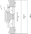
- the SiN passivation structure 12 may also be used with respect to a Metal Oxide Semiconductor Field Effect Transistor (MOSFET) 54, as illustrated in Figure 4 .
- MOSFET Metal Oxide Semiconductor Field Effect Transistor
- the MOSFET 54 includes a substrate 56 and a semiconductor body 58 on a surface of the substrate 56.
- the substrate 56 is preferably formed of SiC, but is not limited thereto.
- the substrate 56 may be formed of other materials such as, for example, Sapphire, AIN, AIGaN, GaN, Si, GaAs, ZnO, and InP.
- the semiconductor body 58 preferably includes one or more epitaxial layers of one or more wideband materials such as, for example, one or more Group III nitrides.
- the semiconductor body 58 may be formed of one or more layers of GaN or AIGaN. However, other Group III nitride materials may be used.
- a source region 60 and a drain region 62 are formed in the semiconductor body 58 by, for example, implanting appropriate ions into a surface of the semiconductor body 58 to achieve a desired doping concentration.
- a source contact 64 is formed by one or more metallic layers on, and preferably directly on, the surface of the semiconductor body 58 adjacent to the source region 60.
- a drain contact 66 is formed by one or more metallic layers on, and preferably directly on, the surface of the semiconductor body 58 adjacent to the drain region 62.
- the source and drain contacts 64 and 66 preferably provide low-resistance ohmic contacts to the source and drain regions 60 and 62, respectively.
- an insulator layer 68 is formed on, and preferably directly on, a surface of the semiconductor body 58 between the source and drain contacts 64 and 66.
- the insulator layer 68 may be, for example, one or more oxide layers (e.g., SiO 2 ).
- a gate contact 70 is formed by one or more metallic layers on, and preferably directly on, a surface of the insulator layer 68 through an opening in the Hydrogen-free SiN layer 28 between the source region 60 and the drain region 62.
- the region within the semiconductor body 58 between the source and drain regions 60 and 62 is a channel region of the MOSFET 54.
- the SiN passivation structure 12 is formed on the surface of the semiconductor body 58, and more specifically on a surface of the insulator layer 68 opposite the semiconductor body 58, between the source contact 64 and the gate contact 70 and between the drain contact 66 and the gate contact 70. In this embodiment, the SiN passivation structure 12 extends over the gate contact 70. As discussed above, the SiN passivation structure 12 includes the Hydrogen-free SiN layers 28 and 30, the Hydrogen barrier layer 32, and the CVD SiN layer 34. Again, the Hydrogen barrier layer 32 and the Hydrogen barrier properties of the Hydrogen-free SiN layers 28 and 30 eliminate or at least mitigate the effects of the Hydrogen in the CVD SiN layer 34. As a result, the performance of the MOSFET 54 substantially improved as compared to the performance of the same MOSFET with conventional CVD SiN passivation.
- Figure 5 illustrates another example of a MOSFET 72 that includes the SiN passivation structure 12.
- the MOSFET 72 includes a substrate 74 and a semiconductor body 76 on a surface of the substrate 74.
- the substrate 74 is preferably formed of SiC, but is not limited thereto.
- the substrate 74 may be formed of other materials such as, for example, Sapphire, AIN, AIGaN, GaN, Si, GaAs, ZnO, and InP.
- the semiconductor body 76 preferably includes one or more epitaxial layers of one or more wideband materials such as, for example, one or more Group III nitrides.
- the semiconductor body 76 may be formed of one or more layers of GaN or AIGaN. However, other Group III nitride materials may be used.
- a source region 78 and a drain region 80 are formed in the semiconductor body 76 by, for example, implanting appropriate ions into a surface of the semiconductor body 76 to achieve a desired doping concentration.
- a source contact 82 is formed by one or more metallic layers on, and preferably directly on, the surface of the semiconductor body 76 adjacent to the source region 78.
- a drain contact 84 is formed by one or more metallic layers on, and preferably directly on, the surface of the semiconductor body 80 adjacent to the drain region 80.
- the source and drain contacts 82 and 84 preferably provide low-resistance ohmic contacts to the source and drain regions 78 and 80, respectively.
- an insulator layer 86, or a gate insulator, for the MOSFET 72 is formed within the SiN passivation structure 12. More specifically, the Hydrogen-free SiN layer 28 is formed on a surface of the semiconductor body 76. An opening in the Hydrogen-free SiN layer 28 for a gate contact 88 of the MOSFET 72 is formed between the source and drain regions 78 and 80. The insulator layer 86 is then formed on a surface of the Hydrogen-free SiN layer 28 and on the surface of the semiconductor body 76 within the opening in the Hydrogen-free SiN layer 28.
- the gate contact 88 is formed on, and preferably directly on, a surface of the insulator layer 86 over the opening in Hydrogen-free SiN layer 28, thereby providing an insulated gate contact for the MOSFET 72.
- the insulator layer 86 may be, for example, one or more oxide layers (e.g., SiO 2 ).
- the gate contact 88 is formed by one or more metallic layers.
- the region within the semiconductor body 76 between the source and drain regions 78 and 80 is a channel region of the MOSFET 72.
- the SiN passivation structure 12 includes the Hydrogen-free SiN layer 30 (which in this embodiment is formed on, and preferably directly on, a surface of the insulator layer 86 opposite the Hydrogen-free SiN layer 28), the Hydrogen barrier layer 32, and the CVD SiN layer 34.
- the Hydrogen barrier layer 32 and the Hydrogen barrier properties of the Hydrogen-free SiN layers 28 and 30 eliminate or at least mitigate the effects of the Hydrogen in the CVD SiN layer 34.
- the performance of the MOSFET 72 is substantially improved as compared to the performance of the same MOSFET with conventional CVD SiN passivation.
Landscapes
- Junction Field-Effect Transistors (AREA)
- Chemical & Material Sciences (AREA)
- Engineering & Computer Science (AREA)
- Ceramic Engineering (AREA)
- Formation Of Insulating Films (AREA)
- Insulated Gate Type Field-Effect Transistor (AREA)
- Electrodes Of Semiconductors (AREA)
Claims (13)
- Halbleitervorrichtung (10, 36, 54, 72), umfassend:einen Halbleiterkörper (16, 58, 76); undeine Passivierungsstruktur (12) auf einer Oberfläche des Halbleiterkörpers, die Passivierungsstruktur umfassend:eine oder mehrere wasserstofffreie Siliciumnitridschichten (28, 30) auf der Oberfläche des Halbleiterkörpers;eine Wasserstoffbarriereschicht (32), die eine sich wiederholende Folge verschiedener Oxidschichten auf einer Oberfläche der einen oder der mehreren wasserstofffreien Siliciumnitridschichten gegenüber dem Halbleiterkörper aufweist; undeine zusätzliche Siliciumnitridschicht (34) auf einer Oberfläche der Wasserstoffschicht gegenüber der einen oder den mehreren wasserstofffreien Siliciumnitridschichten.
- Halbleitervorrichtung nach Anspruch 1, wobei die zusätzliche Siliciumnitridschicht einen Anteil zwischen 15% und 22% Wasserstoff enthält.
- Halbleitervorrichtung nach Anspruch 1, wobei die Halbleitervorrichtung ein Metall-Halbleiter-Feldeffekttransistor (10) ist.
- Halbleitervorrichtung nach Anspruch 1, wobei die Halbleitervorrichtung ein Transistor mit hoher Elektronenmobilität (36) ist.
- Halbleitervorrichtung nach Anspruch 1, ferner umfassend:einen Quellbereich (44) in dem Halbleiterkörper;einen Drainbereich (46) in dem Halbleiterkörper;einen Quellkontakt (48) auf der Oberfläche des Halbleiterkörpers benachbart zu dem Quellbereich;einen Drainkontakt (50) auf der Oberfläche des Halbleiterkörpers benachbart zu dem Drainbereich; undeinen Gatekontakt (52) auf der Oberfläche des Halbleiterkörpers zwischen dem Quellbereich und dem Drainbereich;wobei die Passivierungsstruktur sich auf der Oberfläche des Halbleiterkörpers mindestens zwischen dem Quellkontakt und dem Gatekontakt und zwischen dem Drainkontakt und dem Gatekontakt befindet.
- Halbleitervorrichtung nach Anspruch 1, wobei die Halbleitervorrichtung ein Metalloxid-Halbleiter-Feldeffekttransistor (54, 72) ist.
- Halbleitervorrichtung nach Anspruch 6, ferner umfassend:einen Quellbereich (60) in dem Halbleiterkörper;einen Drainbereich (62) in dem Halbleiterkörper;einen Quellkontakt (64) auf der Oberfläche des Halbleiterkörpers benachbart zu dem Quellbereich;einen Drainkontakt (66) auf der Oberfläche des Halbleiterkörpers benachbart zu dem Drainbereich;eine Isolierschicht (68) auf der Oberfläche des Halbleiterkörpers zwischen dem Quellkontakt und dem Drainkontakt; undeinen Gatekontakt (70) auf einer Oberfläche der Isolierschicht zwischen dem Quellkontakt und dem Drainkontakt gegenüber dem Halbleiterkörper;wobei die Passivierungsstruktur sich auf der Oberfläche der Isolierschicht gegenüber dem Halbleiterkörper mindestens zwischen dem Quellkontakt und dem Gatekontakt und zwischen dem Drainkontakt und dem Gatekontakt befindet.
- Halbleitervorrichtung nach Anspruch 6, ferner umfassend:einen Quellbereich (78) in dem Halbleiterkörper;einen Drainbereich (80) in dem Halbleiterkörper;einen Quellkontakt (82) auf der Oberfläche des Halbleiterkörpers benachbart zu dem Quellbereich; undeinen Drainkontakt (84) auf der Oberfläche des Halbleiterkörpers benachbart zu dem Drainbereich;wobei die Passivierungsstruktur umfasst:eine erste wasserstofffreie Siliciumnitridschicht (28) auf der Oberfläche des Halbleiterkörpers zwischen dem Quellbereich und dem Drainbereich und die eine Öffnung für einen Gatekontakt (88) aufweist;eine Isolierschicht (86) auf einer Oberfläche der ersten wasserstofffreien Siliciumnitridschicht gegenüber dem Halbleiterkörper und auf der Oberfläche des Halbleiterkörpers innerhalb der Öffnung für den Gatekontakt;eine oder mehrere zweite wasserstofffreie Siliciumnitridschichten (30) auf einer Oberfläche der Isolierschicht gegenüber der ersten wasserstofffreien Siliciumnitridschicht und dem Halbleiterkörper;die Wasserstoffbarriereschicht (32) auf einer Oberfläche der einen oder der mehreren zweiten wasserstofffreien Siliciumnitridschichten gegenüber der Isolierschicht; unddie zusätzliche Siliciumnitridschicht (34) auf der Oberfläche der Wasserstoffschicht gegenüber der einen oder den mehreren zweiten wasserstofffreien Siliciumnitridschichten;wobei die Halbleitervorrichtung ferner den Gatekontakt (88) auf der Oberfläche der Isolierschicht zwischen der Isolierschicht und der eine oder den mehreren wasserstofffreien Siliciumnitridschichten und über der Öffnung für den Gatekontakt umfasst.
- Verfahren zum Herstellen einer Passivierungsstruktur für eine Halbleitervorrichtung, umfassend:Bereitstellen einer oder mehrerer wasserstofffreier Siliciumnitridschichten (28) auf einer Oberfläche eines Halbleiterkörpers der Halbleitervorrichtung;Bereitstellen einer Wasserstoffbarriereschicht (32), die eine sich wiederholende Folge verschiedener Oxidschichten auf einer Oberfläche der einen oder der mehreren wasserstofffreien Siliciumnitridschichten gegenüber dem Halbleiterkörper aufweist; undBereitstellen einer zusätzlichen Siliciumnitridschicht (34) auf einer Oberfläche der Wasserstoffschicht gegenüber der einen oder den mehreren wasserstofffreien Siliciumnitridschichten.
- Verfahren nach Anspruch 9, wobei das Bereitstellen der einen oder der mehreren Oxidschichten das Abscheiden der einen oder der mehreren Oxidschichten durch Atomlagenabscheidung umfasst.
- Verfahren nach Anspruch 9, wobei das Bereitstellen der zusätzlichen Siliciumnitridschicht das Bereitstellen der zusätzlichen Siliciumnitridschicht umfasst, sodass die zusätzliche Siliciumnitridschicht einen Anteil zwischen 15% und 22% Wasserstoff enthält.
- Verfahren nach Anspruch 11, wobei das Bereitstellen der zusätzlichen Siliciumnitridschicht das Abscheiden der zusätzlichen Siliciumnitridschicht durch Plasma unterstützte chemische Dampfabscheidung umfasst.
- Verfahren nach Anspruch 11, wobei das Bereitstellen der einen oder der mehreren wasserstofffreien Siliciumnitridschicht das Zerstäuben der einen oder der mehreren wasserstofffreien Siliciumnitridschichten umfasst.
Applications Claiming Priority (2)
| Application Number | Priority Date | Filing Date | Title |
|---|---|---|---|
| US13/644,506 US8994073B2 (en) | 2012-10-04 | 2012-10-04 | Hydrogen mitigation schemes in the passivation of advanced devices |
| PCT/US2013/061798 WO2014055315A1 (en) | 2012-10-04 | 2013-09-26 | Hydrogen mitigation schemes in the passivation of advanced devices |
Publications (2)
| Publication Number | Publication Date |
|---|---|
| EP2904641A1 EP2904641A1 (de) | 2015-08-12 |
| EP2904641B1 true EP2904641B1 (de) | 2019-03-06 |
Family
ID=49322740
Family Applications (1)
| Application Number | Title | Priority Date | Filing Date |
|---|---|---|---|
| EP13774322.5A Active EP2904641B1 (de) | 2012-10-04 | 2013-09-26 | Wasserstoffabschwächungsschemata bei der passivierung fortgeschrittener vorrichtungen |
Country Status (5)
| Country | Link |
|---|---|
| US (1) | US8994073B2 (de) |
| EP (1) | EP2904641B1 (de) |
| JP (1) | JP6305411B2 (de) |
| KR (1) | KR101730279B1 (de) |
| WO (1) | WO2014055315A1 (de) |
Families Citing this family (11)
| Publication number | Priority date | Publication date | Assignee | Title |
|---|---|---|---|---|
| US9991399B2 (en) | 2012-10-04 | 2018-06-05 | Cree, Inc. | Passivation structure for semiconductor devices |
| US9812338B2 (en) | 2013-03-14 | 2017-11-07 | Cree, Inc. | Encapsulation of advanced devices using novel PECVD and ALD schemes |
| US20150333141A1 (en) * | 2013-03-25 | 2015-11-19 | Fudan University | A high electron mobility device based on the gate-first process and the production method thereof |
| JP2015213100A (ja) * | 2014-05-01 | 2015-11-26 | 三菱電機株式会社 | 半導体装置およびその製造方法 |
| JP2016062910A (ja) * | 2014-09-12 | 2016-04-25 | 株式会社東芝 | 半導体装置 |
| JP6536318B2 (ja) * | 2015-09-24 | 2019-07-03 | 三菱電機株式会社 | 半導体装置及びその製造方法 |
| JP6300773B2 (ja) * | 2015-10-23 | 2018-03-28 | 三菱電機株式会社 | 半導体圧力センサ |
| JP6750455B2 (ja) * | 2016-10-28 | 2020-09-02 | 三菱電機株式会社 | 半導体装置及びその製造方法 |
| US12598994B2 (en) * | 2021-06-01 | 2026-04-07 | Wolfspeed, Inc. | Multilayer encapsulation for humidity robustness and related fabrication methods |
| US12218202B2 (en) * | 2021-09-16 | 2025-02-04 | Wolfspeed, Inc. | Semiconductor device incorporating a substrate recess |
| US20230317634A1 (en) * | 2022-04-05 | 2023-10-05 | Applied Materials, Inc. | Coatings with diffusion barriers for corrosion and contamination protection |
Citations (3)
| Publication number | Priority date | Publication date | Assignee | Title |
|---|---|---|---|---|
| US6611014B1 (en) * | 1999-05-14 | 2003-08-26 | Kabushiki Kaisha Toshiba | Semiconductor device having ferroelectric capacitor and hydrogen barrier film and manufacturing method thereof |
| US20070001174A1 (en) * | 2005-06-29 | 2007-01-04 | Zoltan Ring | Passivation of wide band-gap based semiconductor devices with hydrogen-free sputtered nitrides |
| US20070164321A1 (en) * | 2006-01-17 | 2007-07-19 | Cree, Inc. | Methods of fabricating transistors including supported gate electrodes and related devices |
Family Cites Families (86)
| Publication number | Priority date | Publication date | Assignee | Title |
|---|---|---|---|---|
| FR2268355B1 (de) | 1974-04-16 | 1978-01-20 | Thomson Csf | |
| US3895127A (en) | 1974-04-19 | 1975-07-15 | Rca Corp | Method of selectively depositing glass on semiconductor devices |
| US4551353A (en) | 1981-12-30 | 1985-11-05 | Unitrode Corporation | Method for reducing leakage currents in semiconductor devices |
| US4717641A (en) | 1986-01-16 | 1988-01-05 | Motorola Inc. | Method for passivating a semiconductor junction |
| US4799100A (en) | 1987-02-17 | 1989-01-17 | Siliconix Incorporated | Method and apparatus for increasing breakdown of a planar junction |
| US5332697A (en) | 1989-05-31 | 1994-07-26 | Smith Rosemary L | Formation of silicon nitride by nitridation of porous silicon |
| JPH056886A (ja) | 1991-06-27 | 1993-01-14 | Kawasaki Steel Corp | 半導体装置のパツシベーシヨン膜形成方法 |
| JPH05218015A (ja) | 1992-01-30 | 1993-08-27 | Sumitomo Electric Ind Ltd | 半導体装置 |
| JPH05234991A (ja) | 1992-02-26 | 1993-09-10 | Sumitomo Electric Ind Ltd | 半導体装置 |
| GB9206086D0 (en) | 1992-03-20 | 1992-05-06 | Philips Electronics Uk Ltd | Manufacturing electronic devices comprising,e.g.tfts and mims |
| US5612260A (en) | 1992-06-05 | 1997-03-18 | Cree Research, Inc. | Method of obtaining high quality silicon dioxide passivation on silicon carbide and resulting passivated structures |
| US5430324A (en) | 1992-07-23 | 1995-07-04 | Siliconix, Incorporated | High voltage transistor having edge termination utilizing trench technology |
| SE9500013D0 (sv) | 1995-01-03 | 1995-01-03 | Abb Research Ltd | Semiconductor device having a passivation layer |
| US5972801A (en) | 1995-11-08 | 1999-10-26 | Cree Research, Inc. | Process for reducing defects in oxide layers on silicon carbide |
| US6316820B1 (en) | 1997-07-25 | 2001-11-13 | Hughes Electronics Corporation | Passivation layer and process for semiconductor devices |
| US6825501B2 (en) | 1997-08-29 | 2004-11-30 | Cree, Inc. | Robust Group III light emitting diode for high reliability in standard packaging applications |
| US6303969B1 (en) | 1998-05-01 | 2001-10-16 | Allen Tan | Schottky diode with dielectric trench |
| TW471049B (en) | 1998-05-22 | 2002-01-01 | United Microelectronics Corp | Metal gate structure and manufacturing method for metal oxide semiconductor |
| WO2000003345A1 (de) | 1998-07-09 | 2000-01-20 | Infineon Technologies Ag | Halbleiterbauelement mit passivierung |
| US6246076B1 (en) | 1998-08-28 | 2001-06-12 | Cree, Inc. | Layered dielectric on silicon carbide semiconductor structures |
| US6972436B2 (en) | 1998-08-28 | 2005-12-06 | Cree, Inc. | High voltage, high temperature capacitor and interconnection structures |
| JP4361625B2 (ja) | 1998-10-05 | 2009-11-11 | 東京エレクトロン株式会社 | 半導体装置及びその製造方法 |
| US6242784B1 (en) | 1999-06-28 | 2001-06-05 | Intersil Corporation | Edge termination for silicon power devices |
| TW474024B (en) | 1999-08-16 | 2002-01-21 | Cornell Res Foundation Inc | Passivation of GaN based FETs |
| US6373076B1 (en) | 1999-12-07 | 2002-04-16 | Philips Electronics North America Corporation | Passivated silicon carbide devices with low leakage current and method of fabricating |
| US6586781B2 (en) | 2000-02-04 | 2003-07-01 | Cree Lighting Company | Group III nitride based FETs and HEMTs with reduced trapping and method for producing the same |
| US6939756B1 (en) | 2000-03-24 | 2005-09-06 | Vanderbilt University | Inclusion of nitrogen at the silicon dioxide-silicon carbide interace for passivation of interface defects |
| US6630413B2 (en) | 2000-04-28 | 2003-10-07 | Asm Japan K.K. | CVD syntheses of silicon nitride materials |
| US6686616B1 (en) | 2000-05-10 | 2004-02-03 | Cree, Inc. | Silicon carbide metal-semiconductor field effect transistors |
| US6580170B2 (en) | 2000-06-22 | 2003-06-17 | Texas Instruments Incorporated | Semiconductor device protective overcoat with enhanced adhesion to polymeric materials |
| US6396090B1 (en) | 2000-09-22 | 2002-05-28 | Industrial Technology Research Institute | Trench MOS device and termination structure |
| US6690042B2 (en) | 2000-09-27 | 2004-02-10 | Sensor Electronic Technology, Inc. | Metal oxide semiconductor heterostructure field effect transistor |
| US6767843B2 (en) | 2000-10-03 | 2004-07-27 | Cree, Inc. | Method of N2O growth of an oxide layer on a silicon carbide layer |
| US6610366B2 (en) | 2000-10-03 | 2003-08-26 | Cree, Inc. | Method of N2O annealing an oxide layer on a silicon carbide layer |
| US6573128B1 (en) | 2000-11-28 | 2003-06-03 | Cree, Inc. | Epitaxial edge termination for silicon carbide Schottky devices and methods of fabricating silicon carbide devices incorporating same |
| JP4011848B2 (ja) | 2000-12-12 | 2007-11-21 | 関西電力株式会社 | 高耐電圧半導体装置 |
| US6528373B2 (en) | 2001-02-12 | 2003-03-04 | Cree, Inc. | Layered dielectric on silicon carbide semiconductor structures |
| US7141859B2 (en) | 2001-03-29 | 2006-11-28 | Georgia Tech Research Corporation | Porous gas sensors and method of preparation thereof |
| US6849882B2 (en) | 2001-05-11 | 2005-02-01 | Cree Inc. | Group-III nitride based high electron mobility transistor (HEMT) with barrier/spacer layer |
| US6797586B2 (en) | 2001-06-28 | 2004-09-28 | Koninklijke Philips Electronics N.V. | Silicon carbide schottky barrier diode and method of making |
| US6740906B2 (en) | 2001-07-23 | 2004-05-25 | Cree, Inc. | Light emitting diodes including modifications for submount bonding |
| EP2267784B1 (de) | 2001-07-24 | 2020-04-29 | Cree, Inc. | AlGaN/GaN HEMT MIT ISOLIERTEM GATE |
| US6781184B2 (en) * | 2001-11-29 | 2004-08-24 | Symetrix Corporation | Barrier layers for protecting metal oxides from hydrogen degradation |
| US20040160118A1 (en) | 2002-11-08 | 2004-08-19 | Knollenberg Clifford F. | Actuator apparatus and method for improved deflection characteristics |
| US6956239B2 (en) | 2002-11-26 | 2005-10-18 | Cree, Inc. | Transistors having buried p-type layers beneath the source region |
| US6747338B1 (en) | 2002-11-27 | 2004-06-08 | Analog Devices, Inc. | Composite dielectric with improved etch selectivity for high voltage MEMS structures |
| US6983653B2 (en) | 2002-12-13 | 2006-01-10 | Denso Corporation | Flow sensor having thin film portion and method for manufacturing the same |
| US6933544B2 (en) | 2003-01-29 | 2005-08-23 | Kabushiki Kaisha Toshiba | Power semiconductor device |
| WO2005004198A2 (en) | 2003-06-13 | 2005-01-13 | North Carolina State University | Complex oxides for use in semiconductor devices and related methods |
| US7053425B2 (en) | 2003-11-12 | 2006-05-30 | General Electric Company | Gas sensor device |
| DE10358985B3 (de) | 2003-12-16 | 2005-05-19 | Infineon Technologies Ag | Halbleiterbauelement mit einem pn-Übergang und einer auf einer Oberfläche aufgebrachten Passivierungsschicht |
| US7306995B2 (en) * | 2003-12-17 | 2007-12-11 | Texas Instruments Incorporated | Reduced hydrogen sidewall spacer oxide |
| US7045404B2 (en) | 2004-01-16 | 2006-05-16 | Cree, Inc. | Nitride-based transistors with a protective layer and a low-damage recess and methods of fabrication thereof |
| DE102004012884B4 (de) | 2004-03-16 | 2011-07-21 | IXYS Semiconductor GmbH, 68623 | Leistungs-Halbleiterbauelement in Planartechnik |
| JP2005286135A (ja) | 2004-03-30 | 2005-10-13 | Eudyna Devices Inc | 半導体装置および半導体装置の製造方法 |
| US7573078B2 (en) | 2004-05-11 | 2009-08-11 | Cree, Inc. | Wide bandgap transistors with multiple field plates |
| US7550783B2 (en) | 2004-05-11 | 2009-06-23 | Cree, Inc. | Wide bandgap HEMTs with source connected field plates |
| US7332795B2 (en) | 2004-05-22 | 2008-02-19 | Cree, Inc. | Dielectric passivation for semiconductor devices |
| JP2006032911A (ja) | 2004-06-15 | 2006-02-02 | Ngk Insulators Ltd | 半導体積層構造、半導体素子およびhemt素子 |
| US7221039B2 (en) | 2004-06-24 | 2007-05-22 | Taiwan Semiconductor Manufacturing Co., Ltd. | Thin film transistor (TFT) device structure employing silicon rich silicon oxide passivation layer |
| US7547928B2 (en) | 2004-06-30 | 2009-06-16 | Interuniversitair Microelektronica Centrum (Imec) | AlGaN/GaN high electron mobility transistor devices |
| US7297995B2 (en) | 2004-08-24 | 2007-11-20 | Micron Technology, Inc. | Transparent metal shielded isolation for image sensors |
| US7345309B2 (en) | 2004-08-31 | 2008-03-18 | Lockheed Martin Corporation | SiC metal semiconductor field-effect transistor |
| US20060118892A1 (en) | 2004-12-02 | 2006-06-08 | Taiwan Semiconductor Manufacturing Company, Ltd. | Methods and Structures to Produce a Strain-Inducing Layer in a Semiconductor Device |
| US20060145190A1 (en) | 2004-12-31 | 2006-07-06 | Salzman David B | Surface passivation for III-V compound semiconductors |
| SG145706A1 (en) | 2005-02-02 | 2008-09-29 | Agency Science Tech & Res | Method and structure for fabricating iii-v nitride layers on silicon substrates |
| US11791385B2 (en) | 2005-03-11 | 2023-10-17 | Wolfspeed, Inc. | Wide bandgap transistors with gate-source field plates |
| US7598576B2 (en) | 2005-06-29 | 2009-10-06 | Cree, Inc. | Environmentally robust passivation structures for high-voltage silicon carbide semiconductor devices |
| US7855401B2 (en) * | 2005-06-29 | 2010-12-21 | Cree, Inc. | Passivation of wide band-gap based semiconductor devices with hydrogen-free sputtered nitrides |
| US20070018198A1 (en) | 2005-07-20 | 2007-01-25 | Brandes George R | High electron mobility electronic device structures comprising native substrates and methods for making the same |
| US20070018199A1 (en) | 2005-07-20 | 2007-01-25 | Cree, Inc. | Nitride-based transistors and fabrication methods with an etch stop layer |
| US9608102B2 (en) | 2005-12-02 | 2017-03-28 | Infineon Technologies Americas Corp. | Gallium nitride material devices and associated methods |
| US7419892B2 (en) | 2005-12-13 | 2008-09-02 | Cree, Inc. | Semiconductor devices including implanted regions and protective layers and methods of forming the same |
| US7709269B2 (en) | 2006-01-17 | 2010-05-04 | Cree, Inc. | Methods of fabricating transistors including dielectrically-supported gate electrodes |
| US20100279092A1 (en) | 2007-06-01 | 2010-11-04 | Lg Chem, Ltd. | Multiple-layer film and method for manufacturnig the same |
| JP2009094311A (ja) * | 2007-10-10 | 2009-04-30 | Fujitsu Microelectronics Ltd | 半導体装置の製造方法 |
| TWI420722B (zh) * | 2008-01-30 | 2013-12-21 | 歐斯朗奧托半導體股份有限公司 | 具有封裝單元之裝置 |
| JP5714481B2 (ja) | 2008-04-29 | 2015-05-07 | エージェンシー フォー サイエンス,テクノロジー アンド リサーチ | 無機傾斜バリア膜及びそれらの製造方法 |
| US8298628B2 (en) | 2008-06-02 | 2012-10-30 | Air Products And Chemicals, Inc. | Low temperature deposition of silicon-containing films |
| JP2010109276A (ja) * | 2008-10-31 | 2010-05-13 | Sumitomo Electric Ind Ltd | 半導体素子の製造方法および半導体素子 |
| JP4968747B2 (ja) | 2009-02-03 | 2012-07-04 | シャープ株式会社 | Iii−v族化合物半導体素子 |
| JP2010182819A (ja) | 2009-02-04 | 2010-08-19 | Sony Corp | 薄膜トランジスタおよび表示装置 |
| JP4752925B2 (ja) * | 2009-02-04 | 2011-08-17 | ソニー株式会社 | 薄膜トランジスタおよび表示装置 |
| JP2011216771A (ja) | 2010-04-01 | 2011-10-27 | Rohm Co Ltd | 半導体装置およびその製造方法 |
| KR101308480B1 (ko) | 2011-06-14 | 2013-09-16 | 엘지디스플레이 주식회사 | 플라스틱 유기 전계 발광 표시 장치 및 그 제조 방법 |
| KR20130017312A (ko) | 2011-08-10 | 2013-02-20 | 삼성디스플레이 주식회사 | 표시 장치 |
-
2012
- 2012-10-04 US US13/644,506 patent/US8994073B2/en active Active
-
2013
- 2013-09-26 EP EP13774322.5A patent/EP2904641B1/de active Active
- 2013-09-26 WO PCT/US2013/061798 patent/WO2014055315A1/en not_active Ceased
- 2013-09-26 JP JP2015535697A patent/JP6305411B2/ja active Active
- 2013-09-26 KR KR1020157011180A patent/KR101730279B1/ko active Active
Patent Citations (3)
| Publication number | Priority date | Publication date | Assignee | Title |
|---|---|---|---|---|
| US6611014B1 (en) * | 1999-05-14 | 2003-08-26 | Kabushiki Kaisha Toshiba | Semiconductor device having ferroelectric capacitor and hydrogen barrier film and manufacturing method thereof |
| US20070001174A1 (en) * | 2005-06-29 | 2007-01-04 | Zoltan Ring | Passivation of wide band-gap based semiconductor devices with hydrogen-free sputtered nitrides |
| US20070164321A1 (en) * | 2006-01-17 | 2007-07-19 | Cree, Inc. | Methods of fabricating transistors including supported gate electrodes and related devices |
Also Published As
| Publication number | Publication date |
|---|---|
| EP2904641A1 (de) | 2015-08-12 |
| JP6305411B2 (ja) | 2018-04-04 |
| US8994073B2 (en) | 2015-03-31 |
| WO2014055315A1 (en) | 2014-04-10 |
| JP2016506613A (ja) | 2016-03-03 |
| KR101730279B1 (ko) | 2017-05-11 |
| US20140097469A1 (en) | 2014-04-10 |
| KR20150065786A (ko) | 2015-06-15 |
Similar Documents
| Publication | Publication Date | Title |
|---|---|---|
| EP2904641B1 (de) | Wasserstoffabschwächungsschemata bei der passivierung fortgeschrittener vorrichtungen | |
| EP1974373B1 (de) | Verfahren zur herstellung von transistoren mit unterstützten gate-elektroden und entsprechende vorrichtungen | |
| US9337332B2 (en) | III-Nitride insulating-gate transistors with passivation | |
| EP2018663B1 (de) | Herstellungsverfahren von halbleiterbauelemente mit selbst ausrichtenden feuerfesten kontakten | |
| US7709859B2 (en) | Cap layers including aluminum nitride for nitride-based transistors | |
| EP1817798B2 (de) | Kappenschichten und/oder passivierungsschichten für transistoren auf nitridbasis, transistorstrukturen und herstellungsverfahren dafür | |
| KR101344972B1 (ko) | 매립층에 대한 저-저항 콘택을 제공하기 위한 주입된 영역을 포함하는 반도체 소자의 제조 방법 및 관련 소자 | |
| EP1798762A2 (de) | Halbleitervorrichtungen mit ionimplantierten Gebieten und Schutzschichten und Herstellungsverfahren | |
| US20170301765A1 (en) | Semiconductor device and method for manufacturing the same | |
| WO2005117129A1 (en) | Improved dielectric passivation for semiconductor devices | |
| KR20150120357A (ko) | 헤테로기판 상의 iii족-질화물 버퍼 층 구조의 p-도핑 | |
| WO2012047342A2 (en) | Methods of forming semiconductor contacts and related semiconductor devices | |
| TW201431084A (zh) | GaN半導體裝置及其形成方法 | |
| WO2019118473A1 (en) | Methods for transistor epitaxial stack fabrication | |
| WO2016100400A1 (en) | Buffer stack for group iiia-n devices | |
| KR20140139890A (ko) | 질화물 반도체 소자 및 그 제조 방법 | |
| EP2117039B1 (de) | Halbleitervorrichtungen mit flachimplantierten Bereichen und Verfahren zur Bildung davon | |
| WO2016073505A1 (en) | Thermal treated semiconductor/gate dielectric interface for group iiia-n devices | |
| KR20140139346A (ko) | 질화물 반도체 소자 및 그 제조 방법 | |
| KR102080744B1 (ko) | 질화물 반도체 소자 및 그 제조 방법 | |
| KR101364026B1 (ko) | 질화물 반도체 소자 및 그 제조 방법 | |
| KR20130137983A (ko) | 질화물 반도체 소자 및 그 제조 방법 |
Legal Events
| Date | Code | Title | Description |
|---|---|---|---|
| PUAI | Public reference made under article 153(3) epc to a published international application that has entered the european phase |
Free format text: ORIGINAL CODE: 0009012 |
|
| 17P | Request for examination filed |
Effective date: 20150408 |
|
| AK | Designated contracting states |
Kind code of ref document: A1 Designated state(s): AL AT BE BG CH CY CZ DE DK EE ES FI FR GB GR HR HU IE IS IT LI LT LU LV MC MK MT NL NO PL PT RO RS SE SI SK SM TR |
|
| AX | Request for extension of the european patent |
Extension state: BA ME |
|
| DAX | Request for extension of the european patent (deleted) | ||
| STAA | Information on the status of an ep patent application or granted ep patent |
Free format text: STATUS: EXAMINATION IS IN PROGRESS |
|
| 17Q | First examination report despatched |
Effective date: 20170531 |
|
| GRAP | Despatch of communication of intention to grant a patent |
Free format text: ORIGINAL CODE: EPIDOSNIGR1 |
|
| STAA | Information on the status of an ep patent application or granted ep patent |
Free format text: STATUS: GRANT OF PATENT IS INTENDED |
|
| RIC1 | Information provided on ipc code assigned before grant |
Ipc: H01L 29/778 20060101AFI20180829BHEP Ipc: H01L 23/31 20060101ALI20180829BHEP |
|
| INTG | Intention to grant announced |
Effective date: 20180925 |
|
| GRAS | Grant fee paid |
Free format text: ORIGINAL CODE: EPIDOSNIGR3 |
|
| GRAA | (expected) grant |
Free format text: ORIGINAL CODE: 0009210 |
|
| STAA | Information on the status of an ep patent application or granted ep patent |
Free format text: STATUS: THE PATENT HAS BEEN GRANTED |
|
| AK | Designated contracting states |
Kind code of ref document: B1 Designated state(s): AL AT BE BG CH CY CZ DE DK EE ES FI FR GB GR HR HU IE IS IT LI LT LU LV MC MK MT NL NO PL PT RO RS SE SI SK SM TR |
|
| REG | Reference to a national code |
Ref country code: GB Ref legal event code: FG4D |
|
| REG | Reference to a national code |
Ref country code: CH Ref legal event code: EP Ref country code: AT Ref legal event code: REF Ref document number: 1105709 Country of ref document: AT Kind code of ref document: T Effective date: 20190315 |
|
| REG | Reference to a national code |
Ref country code: DE Ref legal event code: R096 Ref document number: 602013051881 Country of ref document: DE |
|
| REG | Reference to a national code |
Ref country code: IE Ref legal event code: FG4D |
|
| REG | Reference to a national code |
Ref country code: NL Ref legal event code: FP |
|
| REG | Reference to a national code |
Ref country code: LT Ref legal event code: MG4D |
|
| PG25 | Lapsed in a contracting state [announced via postgrant information from national office to epo] |
Ref country code: LT Free format text: LAPSE BECAUSE OF FAILURE TO SUBMIT A TRANSLATION OF THE DESCRIPTION OR TO PAY THE FEE WITHIN THE PRESCRIBED TIME-LIMIT Effective date: 20190306 Ref country code: FI Free format text: LAPSE BECAUSE OF FAILURE TO SUBMIT A TRANSLATION OF THE DESCRIPTION OR TO PAY THE FEE WITHIN THE PRESCRIBED TIME-LIMIT Effective date: 20190306 Ref country code: NO Free format text: LAPSE BECAUSE OF FAILURE TO SUBMIT A TRANSLATION OF THE DESCRIPTION OR TO PAY THE FEE WITHIN THE PRESCRIBED TIME-LIMIT Effective date: 20190606 Ref country code: SE Free format text: LAPSE BECAUSE OF FAILURE TO SUBMIT A TRANSLATION OF THE DESCRIPTION OR TO PAY THE FEE WITHIN THE PRESCRIBED TIME-LIMIT Effective date: 20190306 |
|
| PG25 | Lapsed in a contracting state [announced via postgrant information from national office to epo] |
Ref country code: BG Free format text: LAPSE BECAUSE OF FAILURE TO SUBMIT A TRANSLATION OF THE DESCRIPTION OR TO PAY THE FEE WITHIN THE PRESCRIBED TIME-LIMIT Effective date: 20190606 Ref country code: HR Free format text: LAPSE BECAUSE OF FAILURE TO SUBMIT A TRANSLATION OF THE DESCRIPTION OR TO PAY THE FEE WITHIN THE PRESCRIBED TIME-LIMIT Effective date: 20190306 Ref country code: GR Free format text: LAPSE BECAUSE OF FAILURE TO SUBMIT A TRANSLATION OF THE DESCRIPTION OR TO PAY THE FEE WITHIN THE PRESCRIBED TIME-LIMIT Effective date: 20190607 Ref country code: RS Free format text: LAPSE BECAUSE OF FAILURE TO SUBMIT A TRANSLATION OF THE DESCRIPTION OR TO PAY THE FEE WITHIN THE PRESCRIBED TIME-LIMIT Effective date: 20190306 Ref country code: LV Free format text: LAPSE BECAUSE OF FAILURE TO SUBMIT A TRANSLATION OF THE DESCRIPTION OR TO PAY THE FEE WITHIN THE PRESCRIBED TIME-LIMIT Effective date: 20190306 |
|
| REG | Reference to a national code |
Ref country code: AT Ref legal event code: MK05 Ref document number: 1105709 Country of ref document: AT Kind code of ref document: T Effective date: 20190306 |
|
| PG25 | Lapsed in a contracting state [announced via postgrant information from national office to epo] |
Ref country code: RO Free format text: LAPSE BECAUSE OF FAILURE TO SUBMIT A TRANSLATION OF THE DESCRIPTION OR TO PAY THE FEE WITHIN THE PRESCRIBED TIME-LIMIT Effective date: 20190306 Ref country code: SK Free format text: LAPSE BECAUSE OF FAILURE TO SUBMIT A TRANSLATION OF THE DESCRIPTION OR TO PAY THE FEE WITHIN THE PRESCRIBED TIME-LIMIT Effective date: 20190306 Ref country code: CZ Free format text: LAPSE BECAUSE OF FAILURE TO SUBMIT A TRANSLATION OF THE DESCRIPTION OR TO PAY THE FEE WITHIN THE PRESCRIBED TIME-LIMIT Effective date: 20190306 Ref country code: ES Free format text: LAPSE BECAUSE OF FAILURE TO SUBMIT A TRANSLATION OF THE DESCRIPTION OR TO PAY THE FEE WITHIN THE PRESCRIBED TIME-LIMIT Effective date: 20190306 Ref country code: PT Free format text: LAPSE BECAUSE OF FAILURE TO SUBMIT A TRANSLATION OF THE DESCRIPTION OR TO PAY THE FEE WITHIN THE PRESCRIBED TIME-LIMIT Effective date: 20190706 Ref country code: AL Free format text: LAPSE BECAUSE OF FAILURE TO SUBMIT A TRANSLATION OF THE DESCRIPTION OR TO PAY THE FEE WITHIN THE PRESCRIBED TIME-LIMIT Effective date: 20190306 Ref country code: EE Free format text: LAPSE BECAUSE OF FAILURE TO SUBMIT A TRANSLATION OF THE DESCRIPTION OR TO PAY THE FEE WITHIN THE PRESCRIBED TIME-LIMIT Effective date: 20190306 |
|
| PG25 | Lapsed in a contracting state [announced via postgrant information from national office to epo] |
Ref country code: PL Free format text: LAPSE BECAUSE OF FAILURE TO SUBMIT A TRANSLATION OF THE DESCRIPTION OR TO PAY THE FEE WITHIN THE PRESCRIBED TIME-LIMIT Effective date: 20190306 Ref country code: SM Free format text: LAPSE BECAUSE OF FAILURE TO SUBMIT A TRANSLATION OF THE DESCRIPTION OR TO PAY THE FEE WITHIN THE PRESCRIBED TIME-LIMIT Effective date: 20190306 |
|
| REG | Reference to a national code |
Ref country code: DE Ref legal event code: R097 Ref document number: 602013051881 Country of ref document: DE |
|
| PG25 | Lapsed in a contracting state [announced via postgrant information from national office to epo] |
Ref country code: IS Free format text: LAPSE BECAUSE OF FAILURE TO SUBMIT A TRANSLATION OF THE DESCRIPTION OR TO PAY THE FEE WITHIN THE PRESCRIBED TIME-LIMIT Effective date: 20190706 Ref country code: AT Free format text: LAPSE BECAUSE OF FAILURE TO SUBMIT A TRANSLATION OF THE DESCRIPTION OR TO PAY THE FEE WITHIN THE PRESCRIBED TIME-LIMIT Effective date: 20190306 |
|
| PLBE | No opposition filed within time limit |
Free format text: ORIGINAL CODE: 0009261 |
|
| STAA | Information on the status of an ep patent application or granted ep patent |
Free format text: STATUS: NO OPPOSITION FILED WITHIN TIME LIMIT |
|
| PG25 | Lapsed in a contracting state [announced via postgrant information from national office to epo] |
Ref country code: DK Free format text: LAPSE BECAUSE OF FAILURE TO SUBMIT A TRANSLATION OF THE DESCRIPTION OR TO PAY THE FEE WITHIN THE PRESCRIBED TIME-LIMIT Effective date: 20190306 |
|
| 26N | No opposition filed |
Effective date: 20191209 |
|
| PG25 | Lapsed in a contracting state [announced via postgrant information from national office to epo] |
Ref country code: SI Free format text: LAPSE BECAUSE OF FAILURE TO SUBMIT A TRANSLATION OF THE DESCRIPTION OR TO PAY THE FEE WITHIN THE PRESCRIBED TIME-LIMIT Effective date: 20190306 |
|
| PG25 | Lapsed in a contracting state [announced via postgrant information from national office to epo] |
Ref country code: TR Free format text: LAPSE BECAUSE OF FAILURE TO SUBMIT A TRANSLATION OF THE DESCRIPTION OR TO PAY THE FEE WITHIN THE PRESCRIBED TIME-LIMIT Effective date: 20190306 |
|
| PG25 | Lapsed in a contracting state [announced via postgrant information from national office to epo] |
Ref country code: MC Free format text: LAPSE BECAUSE OF FAILURE TO SUBMIT A TRANSLATION OF THE DESCRIPTION OR TO PAY THE FEE WITHIN THE PRESCRIBED TIME-LIMIT Effective date: 20190306 |
|
| REG | Reference to a national code |
Ref country code: CH Ref legal event code: PL |
|
| PG25 | Lapsed in a contracting state [announced via postgrant information from national office to epo] |
Ref country code: LI Free format text: LAPSE BECAUSE OF NON-PAYMENT OF DUE FEES Effective date: 20190930 Ref country code: CH Free format text: LAPSE BECAUSE OF NON-PAYMENT OF DUE FEES Effective date: 20190930 Ref country code: IE Free format text: LAPSE BECAUSE OF NON-PAYMENT OF DUE FEES Effective date: 20190926 Ref country code: LU Free format text: LAPSE BECAUSE OF NON-PAYMENT OF DUE FEES Effective date: 20190926 |
|
| REG | Reference to a national code |
Ref country code: BE Ref legal event code: MM Effective date: 20190930 |
|
| PG25 | Lapsed in a contracting state [announced via postgrant information from national office to epo] |
Ref country code: BE Free format text: LAPSE BECAUSE OF NON-PAYMENT OF DUE FEES Effective date: 20190930 |
|
| GBPC | Gb: european patent ceased through non-payment of renewal fee |
Effective date: 20190926 |
|
| PG25 | Lapsed in a contracting state [announced via postgrant information from national office to epo] |
Ref country code: GB Free format text: LAPSE BECAUSE OF NON-PAYMENT OF DUE FEES Effective date: 20190926 Ref country code: FR Free format text: LAPSE BECAUSE OF NON-PAYMENT OF DUE FEES Effective date: 20190930 |
|
| PG25 | Lapsed in a contracting state [announced via postgrant information from national office to epo] |
Ref country code: CY Free format text: LAPSE BECAUSE OF FAILURE TO SUBMIT A TRANSLATION OF THE DESCRIPTION OR TO PAY THE FEE WITHIN THE PRESCRIBED TIME-LIMIT Effective date: 20190306 |
|
| PG25 | Lapsed in a contracting state [announced via postgrant information from national office to epo] |
Ref country code: MT Free format text: LAPSE BECAUSE OF FAILURE TO SUBMIT A TRANSLATION OF THE DESCRIPTION OR TO PAY THE FEE WITHIN THE PRESCRIBED TIME-LIMIT Effective date: 20190306 Ref country code: HU Free format text: LAPSE BECAUSE OF FAILURE TO SUBMIT A TRANSLATION OF THE DESCRIPTION OR TO PAY THE FEE WITHIN THE PRESCRIBED TIME-LIMIT; INVALID AB INITIO Effective date: 20130926 |
|
| REG | Reference to a national code |
Ref country code: NL Ref legal event code: HC Owner name: WOLFSPEED, INC.; US Free format text: DETAILS ASSIGNMENT: CHANGE OF OWNER(S), CHANGE OF OWNER(S) NAME; FORMER OWNER NAME: CREE, INC. Effective date: 20220311 |
|
| PG25 | Lapsed in a contracting state [announced via postgrant information from national office to epo] |
Ref country code: MK Free format text: LAPSE BECAUSE OF FAILURE TO SUBMIT A TRANSLATION OF THE DESCRIPTION OR TO PAY THE FEE WITHIN THE PRESCRIBED TIME-LIMIT Effective date: 20190306 |
|
| REG | Reference to a national code |
Ref country code: DE Ref legal event code: R081 Ref document number: 602013051881 Country of ref document: DE Owner name: WOLFSPEED, INC., DURHAM, US Free format text: FORMER OWNER: CREE, INC., DURHAM, N.C., US |
|
| REG | Reference to a national code |
Ref country code: DE Ref legal event code: R079 Ref document number: 602013051881 Country of ref document: DE Free format text: PREVIOUS MAIN CLASS: H01L0029778000 Ipc: H10D0030470000 |
|
| PGFP | Annual fee paid to national office [announced via postgrant information from national office to epo] |
Ref country code: DE Payment date: 20250929 Year of fee payment: 13 |
|
| PGFP | Annual fee paid to national office [announced via postgrant information from national office to epo] |
Ref country code: NL Payment date: 20250926 Year of fee payment: 13 Ref country code: IT Payment date: 20250919 Year of fee payment: 13 |