EP2903048B1 - Verbindung für organische elektrolumineszenzelemente und organisches elektrolumineszenzelement - Google Patents
Verbindung für organische elektrolumineszenzelemente und organisches elektrolumineszenzelement Download PDFInfo
- Publication number
- EP2903048B1 EP2903048B1 EP13841725.8A EP13841725A EP2903048B1 EP 2903048 B1 EP2903048 B1 EP 2903048B1 EP 13841725 A EP13841725 A EP 13841725A EP 2903048 B1 EP2903048 B1 EP 2903048B1
- Authority
- EP
- European Patent Office
- Prior art keywords
- group
- carbon atoms
- substituted
- compound
- unsubstituted aromatic
- Prior art date
- Legal status (The legal status is an assumption and is not a legal conclusion. Google has not performed a legal analysis and makes no representation as to the accuracy of the status listed.)
- Not-in-force
Links
- 150000001875 compounds Chemical class 0.000 title claims description 82
- 125000004432 carbon atom Chemical group C* 0.000 claims description 187
- 239000010410 layer Substances 0.000 claims description 152
- 239000000463 material Substances 0.000 claims description 84
- 125000002029 aromatic hydrocarbon group Chemical group 0.000 claims description 37
- 125000006615 aromatic heterocyclic group Chemical group 0.000 claims description 36
- 125000003118 aryl group Chemical group 0.000 claims description 34
- ZOXJGFHDIHLPTG-UHFFFAOYSA-N Boron Chemical compound [B] ZOXJGFHDIHLPTG-UHFFFAOYSA-N 0.000 claims description 24
- 229910052796 boron Inorganic materials 0.000 claims description 24
- 125000001424 substituent group Chemical group 0.000 claims description 23
- 239000002019 doping agent Substances 0.000 claims description 19
- 125000000217 alkyl group Chemical group 0.000 claims description 18
- YZCKVEUIGOORGS-OUBTZVSYSA-N Deuterium Chemical compound [2H] YZCKVEUIGOORGS-OUBTZVSYSA-N 0.000 claims description 15
- 229910052805 deuterium Inorganic materials 0.000 claims description 15
- 239000012044 organic layer Substances 0.000 claims description 15
- 125000003342 alkenyl group Chemical group 0.000 claims description 14
- 125000000304 alkynyl group Chemical group 0.000 claims description 14
- 125000003545 alkoxy group Chemical group 0.000 claims description 13
- 125000003710 aryl alkyl group Chemical group 0.000 claims description 10
- 125000004986 diarylamino group Chemical group 0.000 claims description 10
- 125000002252 acyl group Chemical group 0.000 claims description 9
- 125000004453 alkoxycarbonyl group Chemical group 0.000 claims description 9
- 125000004390 alkyl sulfonyl group Chemical group 0.000 claims description 9
- 125000004414 alkyl thio group Chemical group 0.000 claims description 9
- 125000004663 dialkyl amino group Chemical group 0.000 claims description 9
- 125000001188 haloalkyl group Chemical group 0.000 claims description 9
- 125000000951 phenoxy group Chemical group [H]C1=C([H])C([H])=C(O*)C([H])=C1[H] 0.000 claims description 9
- 125000000623 heterocyclic group Chemical group 0.000 claims description 8
- 125000002887 hydroxy group Chemical group [H]O* 0.000 claims description 7
- 125000003368 amide group Chemical group 0.000 claims description 6
- 125000003277 amino group Chemical group 0.000 claims description 6
- 125000003178 carboxy group Chemical group [H]OC(*)=O 0.000 claims description 6
- 125000004093 cyano group Chemical group *C#N 0.000 claims description 6
- 125000000449 nitro group Chemical group [O-][N+](*)=O 0.000 claims description 6
- WKBOTKDWSSQWDR-UHFFFAOYSA-N Bromine atom Chemical compound [Br] WKBOTKDWSSQWDR-UHFFFAOYSA-N 0.000 claims description 5
- ZAMOUSCENKQFHK-UHFFFAOYSA-N Chlorine atom Chemical compound [Cl] ZAMOUSCENKQFHK-UHFFFAOYSA-N 0.000 claims description 5
- PXGOKWXKJXAPGV-UHFFFAOYSA-N Fluorine Chemical compound FF PXGOKWXKJXAPGV-UHFFFAOYSA-N 0.000 claims description 5
- GDTBXPJZTBHREO-UHFFFAOYSA-N bromine Substances BrBr GDTBXPJZTBHREO-UHFFFAOYSA-N 0.000 claims description 5
- 229910052794 bromium Inorganic materials 0.000 claims description 5
- 239000000460 chlorine Substances 0.000 claims description 5
- 229910052801 chlorine Inorganic materials 0.000 claims description 5
- 239000011737 fluorine Substances 0.000 claims description 5
- 229910052731 fluorine Inorganic materials 0.000 claims description 5
- 150000002431 hydrogen Chemical class 0.000 claims description 4
- 229910052739 hydrogen Inorganic materials 0.000 claims description 4
- 239000001257 hydrogen Substances 0.000 claims description 4
- PJVZQNVOUCOJGE-CALCHBBNSA-N chembl289853 Chemical compound N1([C@H]2CC[C@H](O2)N2[C]3C=CC=CC3=C3C2=C11)C2=CC=C[CH]C2=C1C1=C3C(=O)N(C)C1=O PJVZQNVOUCOJGE-CALCHBBNSA-N 0.000 description 28
- -1 carbazole compound Chemical class 0.000 description 26
- 230000003111 delayed effect Effects 0.000 description 20
- VVVPGLRKXQSQSZ-UHFFFAOYSA-N indolo[3,2-c]carbazole Chemical class C1=CC=CC2=NC3=C4C5=CC=CC=C5N=C4C=CC3=C21 VVVPGLRKXQSQSZ-UHFFFAOYSA-N 0.000 description 18
- 239000000203 mixture Substances 0.000 description 18
- 229910052751 metal Inorganic materials 0.000 description 17
- 239000002184 metal Substances 0.000 description 17
- 239000000126 substance Substances 0.000 description 13
- UEEXRMUCXBPYOV-UHFFFAOYSA-N iridium;2-phenylpyridine Chemical compound [Ir].C1=CC=CC=C1C1=CC=CC=N1.C1=CC=CC=C1C1=CC=CC=N1.C1=CC=CC=C1C1=CC=CC=N1 UEEXRMUCXBPYOV-UHFFFAOYSA-N 0.000 description 10
- 239000000758 substrate Substances 0.000 description 10
- GVEPBJHOBDJJJI-UHFFFAOYSA-N fluoranthrene Natural products C1=CC(C2=CC=CC=C22)=C3C2=CC=CC3=C1 GVEPBJHOBDJJJI-UHFFFAOYSA-N 0.000 description 9
- FYYHWMGAXLPEAU-UHFFFAOYSA-N Magnesium Chemical compound [Mg] FYYHWMGAXLPEAU-UHFFFAOYSA-N 0.000 description 8
- YTPLMLYBLZKORZ-UHFFFAOYSA-N Thiophene Chemical compound C=1C=CSC=1 YTPLMLYBLZKORZ-UHFFFAOYSA-N 0.000 description 8
- 229910052782 aluminium Inorganic materials 0.000 description 8
- XAGFODPZIPBFFR-UHFFFAOYSA-N aluminium Chemical compound [Al] XAGFODPZIPBFFR-UHFFFAOYSA-N 0.000 description 8
- MWPLVEDNUUSJAV-UHFFFAOYSA-N anthracene Chemical compound C1=CC=CC2=CC3=CC=CC=C3C=C21 MWPLVEDNUUSJAV-UHFFFAOYSA-N 0.000 description 8
- 239000011777 magnesium Substances 0.000 description 8
- 229910052749 magnesium Inorganic materials 0.000 description 8
- VFUDMQLBKNMONU-UHFFFAOYSA-N 9-[4-(4-carbazol-9-ylphenyl)phenyl]carbazole Chemical group C12=CC=CC=C2C2=CC=CC=C2N1C1=CC=C(C=2C=CC(=CC=2)N2C3=CC=CC=C3C3=CC=CC=C32)C=C1 VFUDMQLBKNMONU-UHFFFAOYSA-N 0.000 description 7
- UHOVQNZJYSORNB-UHFFFAOYSA-N Benzene Chemical compound C1=CC=CC=C1 UHOVQNZJYSORNB-UHFFFAOYSA-N 0.000 description 7
- 0 CC([C@@](C=C(B(C(C)=CC=CC#C)c1ccccc1)C)c(cc1)c2c(c3ccccc33)c1[n]3-c(cc1c3cc(B(C4=CC5=*[C@]5C=C4)C4=CCC=CC=C4)ccc33)ccc1[n]3-c1ccccc1)N2c(cc1)cc(C2C=C(B(C3=CC=CCC3)c3ccccc3)C=C*22)c1N2C1C=CC=CC1 Chemical compound CC([C@@](C=C(B(C(C)=CC=CC#C)c1ccccc1)C)c(cc1)c2c(c3ccccc33)c1[n]3-c(cc1c3cc(B(C4=CC5=*[C@]5C=C4)C4=CCC=CC=C4)ccc33)ccc1[n]3-c1ccccc1)N2c(cc1)cc(C2C=C(B(C3=CC=CCC3)c3ccccc3)C=C*22)c1N2C1C=CC=CC1 0.000 description 7
- 150000001716 carbazoles Chemical class 0.000 description 7
- 150000004866 oxadiazoles Chemical class 0.000 description 7
- YBYIRNPNPLQARY-UHFFFAOYSA-N 1H-indene Chemical compound C1=CC=C2CC=CC2=C1 YBYIRNPNPLQARY-UHFFFAOYSA-N 0.000 description 6
- UFWIBTONFRDIAS-UHFFFAOYSA-N Naphthalene Chemical compound C1=CC=CC2=CC=CC=C21 UFWIBTONFRDIAS-UHFFFAOYSA-N 0.000 description 6
- WYURNTSHIVDZCO-UHFFFAOYSA-N Tetrahydrofuran Chemical compound C1CCOC1 WYURNTSHIVDZCO-UHFFFAOYSA-N 0.000 description 6
- 150000004945 aromatic hydrocarbons Chemical group 0.000 description 6
- WDECIBYCCFPHNR-UHFFFAOYSA-N chrysene Chemical compound C1=CC=CC2=CC=C3C4=CC=CC=C4C=CC3=C21 WDECIBYCCFPHNR-UHFFFAOYSA-N 0.000 description 6
- 230000005281 excited state Effects 0.000 description 6
- RAXXELZNTBOGNW-UHFFFAOYSA-N imidazole Natural products C1=CNC=N1 RAXXELZNTBOGNW-UHFFFAOYSA-N 0.000 description 6
- YNPNZTXNASCQKK-UHFFFAOYSA-N phenanthrene Chemical compound C1=CC=C2C3=CC=CC=C3C=CC2=C1 YNPNZTXNASCQKK-UHFFFAOYSA-N 0.000 description 6
- 229920000642 polymer Chemical class 0.000 description 6
- BBEAQIROQSPTKN-UHFFFAOYSA-N pyrene Chemical compound C1=CC=C2C=CC3=CC=CC4=CC=C1C2=C43 BBEAQIROQSPTKN-UHFFFAOYSA-N 0.000 description 6
- YLQBMQCUIZJEEH-UHFFFAOYSA-N Furan Chemical compound C=1C=COC=1 YLQBMQCUIZJEEH-UHFFFAOYSA-N 0.000 description 5
- 230000015572 biosynthetic process Effects 0.000 description 5
- 230000000052 comparative effect Effects 0.000 description 5
- 150000004696 coordination complex Chemical class 0.000 description 5
- 239000010408 film Substances 0.000 description 5
- 238000000034 method Methods 0.000 description 5
- 229910052757 nitrogen Inorganic materials 0.000 description 5
- 238000003786 synthesis reaction Methods 0.000 description 5
- 239000010409 thin film Substances 0.000 description 5
- PAYRUJLWNCNPSJ-UHFFFAOYSA-N Aniline Chemical compound NC1=CC=CC=C1 PAYRUJLWNCNPSJ-UHFFFAOYSA-N 0.000 description 4
- 150000004982 aromatic amines Chemical class 0.000 description 4
- 150000001491 aromatic compounds Chemical class 0.000 description 4
- IOJUPLGTWVMSFF-UHFFFAOYSA-N benzothiazole Chemical compound C1=CC=C2SC=NC2=C1 IOJUPLGTWVMSFF-UHFFFAOYSA-N 0.000 description 4
- 125000004435 hydrogen atom Chemical group [H]* 0.000 description 4
- 238000004020 luminiscence type Methods 0.000 description 4
- TWNQGVIAIRXVLR-UHFFFAOYSA-N oxo(oxoalumanyloxy)alumane Chemical compound O=[Al]O[Al]=O TWNQGVIAIRXVLR-UHFFFAOYSA-N 0.000 description 4
- 229920000553 poly(phenylenevinylene) Polymers 0.000 description 4
- 229920000123 polythiophene Polymers 0.000 description 4
- 229930192474 thiophene Natural products 0.000 description 4
- TVIVIEFSHFOWTE-UHFFFAOYSA-K tri(quinolin-8-yloxy)alumane Chemical compound [Al+3].C1=CN=C2C([O-])=CC=CC2=C1.C1=CN=C2C([O-])=CC=CC2=C1.C1=CN=C2C([O-])=CC=CC2=C1 TVIVIEFSHFOWTE-UHFFFAOYSA-K 0.000 description 4
- BCMCBBGGLRIHSE-UHFFFAOYSA-N 1,3-benzoxazole Chemical compound C1=CC=C2OC=NC2=C1 BCMCBBGGLRIHSE-UHFFFAOYSA-N 0.000 description 3
- KLCLIOISYBHYDZ-UHFFFAOYSA-N 1,4,4-triphenylbuta-1,3-dienylbenzene Chemical class C=1C=CC=CC=1C(C=1C=CC=CC=1)=CC=C(C=1C=CC=CC=1)C1=CC=CC=C1 KLCLIOISYBHYDZ-UHFFFAOYSA-N 0.000 description 3
- CFNMUZCFSDMZPQ-GHXNOFRVSA-N 7-[(z)-3-methyl-4-(4-methyl-5-oxo-2h-furan-2-yl)but-2-enoxy]chromen-2-one Chemical compound C=1C=C2C=CC(=O)OC2=CC=1OC/C=C(/C)CC1OC(=O)C(C)=C1 CFNMUZCFSDMZPQ-GHXNOFRVSA-N 0.000 description 3
- UJOBWOGCFQCDNV-UHFFFAOYSA-N Carbazole Natural products C1=CC=C2C3=CC=CC=C3NC2=C1 UJOBWOGCFQCDNV-UHFFFAOYSA-N 0.000 description 3
- XEKOWRVHYACXOJ-UHFFFAOYSA-N Ethyl acetate Chemical compound CCOC(C)=O XEKOWRVHYACXOJ-UHFFFAOYSA-N 0.000 description 3
- WHXSMMKQMYFTQS-UHFFFAOYSA-N Lithium Chemical compound [Li] WHXSMMKQMYFTQS-UHFFFAOYSA-N 0.000 description 3
- CSNNHWWHGAXBCP-UHFFFAOYSA-L Magnesium sulfate Chemical compound [Mg+2].[O-][S+2]([O-])([O-])[O-] CSNNHWWHGAXBCP-UHFFFAOYSA-L 0.000 description 3
- SLGBZMMZGDRARJ-UHFFFAOYSA-N Triphenylene Natural products C1=CC=C2C3=CC=CC=C3C3=CC=CC=C3C2=C1 SLGBZMMZGDRARJ-UHFFFAOYSA-N 0.000 description 3
- 239000007983 Tris buffer Substances 0.000 description 3
- REDXJYDRNCIFBQ-UHFFFAOYSA-N aluminium(3+) Chemical compound [Al+3] REDXJYDRNCIFBQ-UHFFFAOYSA-N 0.000 description 3
- XSCHRSMBECNVNS-UHFFFAOYSA-N benzopyrazine Natural products N1=CC=NC2=CC=CC=C21 XSCHRSMBECNVNS-UHFFFAOYSA-N 0.000 description 3
- 230000000903 blocking effect Effects 0.000 description 3
- 238000006243 chemical reaction Methods 0.000 description 3
- ZSWFCLXCOIISFI-UHFFFAOYSA-N cyclopentadiene Chemical class C1C=CC=C1 ZSWFCLXCOIISFI-UHFFFAOYSA-N 0.000 description 3
- 238000000295 emission spectrum Methods 0.000 description 3
- 229910052738 indium Inorganic materials 0.000 description 3
- APFVFJFRJDLVQX-UHFFFAOYSA-N indium atom Chemical compound [In] APFVFJFRJDLVQX-UHFFFAOYSA-N 0.000 description 3
- 229960005544 indolocarbazole Drugs 0.000 description 3
- 229910052744 lithium Inorganic materials 0.000 description 3
- DGBWPZSGHAXYGK-UHFFFAOYSA-N perinone Chemical class C12=NC3=CC=CC=C3N2C(=O)C2=CC=C3C4=C2C1=CC=C4C(=O)N1C2=CC=CC=C2N=C13 DGBWPZSGHAXYGK-UHFFFAOYSA-N 0.000 description 3
- 125000002080 perylenyl group Chemical group C1(=CC=C2C=CC=C3C4=CC=CC5=CC=CC(C1=C23)=C45)* 0.000 description 3
- CSHWQDPOILHKBI-UHFFFAOYSA-N peryrene Natural products C1=CC(C2=CC=CC=3C2=C2C=CC=3)=C3C2=CC=CC3=C1 CSHWQDPOILHKBI-UHFFFAOYSA-N 0.000 description 3
- 229920003227 poly(N-vinyl carbazole) Polymers 0.000 description 3
- 229920002098 polyfluorene Polymers 0.000 description 3
- 150000005255 pyrrolopyridines Chemical class 0.000 description 3
- 229910052709 silver Inorganic materials 0.000 description 3
- 239000004332 silver Substances 0.000 description 3
- 239000007787 solid Substances 0.000 description 3
- 239000002904 solvent Substances 0.000 description 3
- 238000004544 sputter deposition Methods 0.000 description 3
- IFLREYGFSNHWGE-UHFFFAOYSA-N tetracene Chemical compound C1=CC=CC2=CC3=CC4=CC=CC=C4C=C3C=C21 IFLREYGFSNHWGE-UHFFFAOYSA-N 0.000 description 3
- QKTRRACPJVYJNU-UHFFFAOYSA-N thiadiazolo[5,4-b]pyridine Chemical class C1=CN=C2SN=NC2=C1 QKTRRACPJVYJNU-UHFFFAOYSA-N 0.000 description 3
- 125000005580 triphenylene group Chemical group 0.000 description 3
- 238000007740 vapor deposition Methods 0.000 description 3
- DXBHBZVCASKNBY-UHFFFAOYSA-N 1,2-Benz(a)anthracene Chemical compound C1=CC=C2C3=CC4=CC=CC=C4C=C3C=CC2=C1 DXBHBZVCASKNBY-UHFFFAOYSA-N 0.000 description 2
- NGQSLSMAEVWNPU-YTEMWHBBSA-N 1,2-bis[(e)-2-phenylethenyl]benzene Chemical class C=1C=CC=CC=1/C=C/C1=CC=CC=C1\C=C\C1=CC=CC=C1 NGQSLSMAEVWNPU-YTEMWHBBSA-N 0.000 description 2
- CYSGHNMQYZDMIA-UHFFFAOYSA-N 1,3-Dimethyl-2-imidazolidinon Chemical compound CN1CCN(C)C1=O CYSGHNMQYZDMIA-UHFFFAOYSA-N 0.000 description 2
- 125000001140 1,4-phenylene group Chemical group [H]C1=C([H])C([*:2])=C([H])C([H])=C1[*:1] 0.000 description 2
- 238000005160 1H NMR spectroscopy Methods 0.000 description 2
- MVWPVABZQQJTPL-UHFFFAOYSA-N 2,3-diphenylcyclohexa-2,5-diene-1,4-dione Chemical class O=C1C=CC(=O)C(C=2C=CC=CC=2)=C1C1=CC=CC=C1 MVWPVABZQQJTPL-UHFFFAOYSA-N 0.000 description 2
- UXGVMFHEKMGWMA-UHFFFAOYSA-N 2-benzofuran Chemical compound C1=CC=CC2=COC=C21 UXGVMFHEKMGWMA-UHFFFAOYSA-N 0.000 description 2
- KDCGOANMDULRCW-UHFFFAOYSA-N 7H-purine Chemical compound N1=CNC2=NC=NC2=C1 KDCGOANMDULRCW-UHFFFAOYSA-N 0.000 description 2
- YFIJJNAKSZUOLT-UHFFFAOYSA-N Anthanthrene Chemical compound C1=C(C2=C34)C=CC=C2C=CC3=CC2=CC=CC3=CC=C1C4=C32 YFIJJNAKSZUOLT-UHFFFAOYSA-N 0.000 description 2
- RYGMFSIKBFXOCR-UHFFFAOYSA-N Copper Chemical compound [Cu] RYGMFSIKBFXOCR-UHFFFAOYSA-N 0.000 description 2
- SIKJAQJRHWYJAI-UHFFFAOYSA-N Indole Chemical compound C1=CC=C2NC=CC2=C1 SIKJAQJRHWYJAI-UHFFFAOYSA-N 0.000 description 2
- KDLHZDBZIXYQEI-UHFFFAOYSA-N Palladium Chemical compound [Pd] KDLHZDBZIXYQEI-UHFFFAOYSA-N 0.000 description 2
- PCNDJXKNXGMECE-UHFFFAOYSA-N Phenazine Natural products C1=CC=CC2=NC3=CC=CC=C3N=C21 PCNDJXKNXGMECE-UHFFFAOYSA-N 0.000 description 2
- 229920000265 Polyparaphenylene Polymers 0.000 description 2
- KYQCOXFCLRTKLS-UHFFFAOYSA-N Pyrazine Chemical compound C1=CN=CC=N1 KYQCOXFCLRTKLS-UHFFFAOYSA-N 0.000 description 2
- JUJWROOIHBZHMG-UHFFFAOYSA-N Pyridine Chemical compound C1=CC=NC=C1 JUJWROOIHBZHMG-UHFFFAOYSA-N 0.000 description 2
- KAESVJOAVNADME-UHFFFAOYSA-N Pyrrole Chemical compound C=1C=CNC=1 KAESVJOAVNADME-UHFFFAOYSA-N 0.000 description 2
- SMWDFEZZVXVKRB-UHFFFAOYSA-N Quinoline Chemical compound N1=CC=CC2=CC=CC=C21 SMWDFEZZVXVKRB-UHFFFAOYSA-N 0.000 description 2
- DZBUGLKDJFMEHC-UHFFFAOYSA-N acridine Chemical compound C1=CC=CC2=CC3=CC=CC=C3N=C21 DZBUGLKDJFMEHC-UHFFFAOYSA-N 0.000 description 2
- 229910045601 alloy Inorganic materials 0.000 description 2
- 239000000956 alloy Substances 0.000 description 2
- 150000008425 anthrones Chemical class 0.000 description 2
- 150000004984 aromatic diamines Chemical class 0.000 description 2
- JTRPLRMCBJSBJV-UHFFFAOYSA-N benzo[a]tetracene Chemical compound C1=CC=C2C3=CC4=CC5=CC=CC=C5C=C4C=C3C=CC2=C1 JTRPLRMCBJSBJV-UHFFFAOYSA-N 0.000 description 2
- 229920001577 copolymer Polymers 0.000 description 2
- 229910052802 copper Inorganic materials 0.000 description 2
- 239000010949 copper Substances 0.000 description 2
- TXCDCPKCNAJMEE-UHFFFAOYSA-N dibenzofuran Chemical compound C1=CC=C2C3=CC=CC=C3OC2=C1 TXCDCPKCNAJMEE-UHFFFAOYSA-N 0.000 description 2
- 150000004826 dibenzofurans Chemical class 0.000 description 2
- IYYZUPMFVPLQIF-UHFFFAOYSA-N dibenzothiophene Chemical compound C1=CC=C2C3=CC=CC=C3SC2=C1 IYYZUPMFVPLQIF-UHFFFAOYSA-N 0.000 description 2
- 230000000694 effects Effects 0.000 description 2
- 230000005684 electric field Effects 0.000 description 2
- 230000005284 excitation Effects 0.000 description 2
- 238000001914 filtration Methods 0.000 description 2
- RMBPEFMHABBEKP-UHFFFAOYSA-N fluorene Chemical compound C1=CC=C2C3=C[CH]C=CC3=CC2=C1 RMBPEFMHABBEKP-UHFFFAOYSA-N 0.000 description 2
- 150000008376 fluorenones Chemical class 0.000 description 2
- 239000011521 glass Substances 0.000 description 2
- 239000010931 gold Substances 0.000 description 2
- 150000007857 hydrazones Chemical class 0.000 description 2
- 150000002460 imidazoles Chemical class 0.000 description 2
- 150000002469 indenes Chemical class 0.000 description 2
- 238000002347 injection Methods 0.000 description 2
- 239000007924 injection Substances 0.000 description 2
- 229910052741 iridium Inorganic materials 0.000 description 2
- GKOZUEZYRPOHIO-UHFFFAOYSA-N iridium atom Chemical compound [Ir] GKOZUEZYRPOHIO-UHFFFAOYSA-N 0.000 description 2
- AWJUIBRHMBBTKR-UHFFFAOYSA-N isoquinoline Chemical compound C1=NC=CC2=CC=CC=C21 AWJUIBRHMBBTKR-UHFFFAOYSA-N 0.000 description 2
- 238000010030 laminating Methods 0.000 description 2
- 238000004768 lowest unoccupied molecular orbital Methods 0.000 description 2
- 238000004519 manufacturing process Methods 0.000 description 2
- 238000005259 measurement Methods 0.000 description 2
- 150000002739 metals Chemical class 0.000 description 2
- 239000012299 nitrogen atmosphere Substances 0.000 description 2
- NIHNNTQXNPWCJQ-UHFFFAOYSA-N o-biphenylenemethane Natural products C1=CC=C2CC3=CC=CC=C3C2=C1 NIHNNTQXNPWCJQ-UHFFFAOYSA-N 0.000 description 2
- NFBOHOGPQUYFRF-UHFFFAOYSA-N oxanthrene Chemical compound C1=CC=C2OC3=CC=CC=C3OC2=C1 NFBOHOGPQUYFRF-UHFFFAOYSA-N 0.000 description 2
- 150000007978 oxazole derivatives Chemical class 0.000 description 2
- 230000003647 oxidation Effects 0.000 description 2
- 238000007254 oxidation reaction Methods 0.000 description 2
- RDOWQLZANAYVLL-UHFFFAOYSA-N phenanthridine Chemical compound C1=CC=C2C3=CC=CC=C3C=NC2=C1 RDOWQLZANAYVLL-UHFFFAOYSA-N 0.000 description 2
- 150000004986 phenylenediamines Chemical class 0.000 description 2
- IEQIEDJGQAUEQZ-UHFFFAOYSA-N phthalocyanine Chemical class N1C(N=C2C3=CC=CC=C3C(N=C3C4=CC=CC=C4C(=N4)N3)=N2)=C(C=CC=C2)C2=C1N=C1C2=CC=CC=C2C4=N1 IEQIEDJGQAUEQZ-UHFFFAOYSA-N 0.000 description 2
- BASFCYQUMIYNBI-UHFFFAOYSA-N platinum Chemical compound [Pt] BASFCYQUMIYNBI-UHFFFAOYSA-N 0.000 description 2
- BWHMMNNQKKPAPP-UHFFFAOYSA-L potassium carbonate Chemical compound [K+].[K+].[O-]C([O-])=O BWHMMNNQKKPAPP-UHFFFAOYSA-L 0.000 description 2
- JEXVQSWXXUJEMA-UHFFFAOYSA-N pyrazol-3-one Chemical class O=C1C=CN=N1 JEXVQSWXXUJEMA-UHFFFAOYSA-N 0.000 description 2
- 150000003219 pyrazolines Chemical class 0.000 description 2
- RQGPLDBZHMVWCH-UHFFFAOYSA-N pyrrolo[3,2-b]pyrrole Chemical class C1=NC2=CC=NC2=C1 RQGPLDBZHMVWCH-UHFFFAOYSA-N 0.000 description 2
- MCJGNVYPOGVAJF-UHFFFAOYSA-N quinolin-8-ol Chemical class C1=CN=C2C(O)=CC=CC2=C1 MCJGNVYPOGVAJF-UHFFFAOYSA-N 0.000 description 2
- 229910052761 rare earth metal Inorganic materials 0.000 description 2
- 150000002910 rare earth metals Chemical class 0.000 description 2
- 238000005215 recombination Methods 0.000 description 2
- 230000006798 recombination Effects 0.000 description 2
- 238000010898 silica gel chromatography Methods 0.000 description 2
- 239000000243 solution Substances 0.000 description 2
- PJANXHGTPQOBST-UHFFFAOYSA-N stilbene Chemical class C=1C=CC=CC=1C=CC1=CC=CC=C1 PJANXHGTPQOBST-UHFFFAOYSA-N 0.000 description 2
- IBBLKSWSCDAPIF-UHFFFAOYSA-N thiopyran Chemical compound S1C=CC=C=C1 IBBLKSWSCDAPIF-UHFFFAOYSA-N 0.000 description 2
- XOLBLPGZBRYERU-UHFFFAOYSA-N tin dioxide Chemical compound O=[Sn]=O XOLBLPGZBRYERU-UHFFFAOYSA-N 0.000 description 2
- 229910052723 transition metal Inorganic materials 0.000 description 2
- 150000003624 transition metals Chemical class 0.000 description 2
- 239000012780 transparent material Substances 0.000 description 2
- 150000003918 triazines Chemical class 0.000 description 2
- 150000003852 triazoles Chemical class 0.000 description 2
- UWRZIZXBOLBCON-VOTSOKGWSA-N (e)-2-phenylethenamine Chemical class N\C=C\C1=CC=CC=C1 UWRZIZXBOLBCON-VOTSOKGWSA-N 0.000 description 1
- JYEUMXHLPRZUAT-UHFFFAOYSA-N 1,2,3-triazine Chemical compound C1=CN=NN=C1 JYEUMXHLPRZUAT-UHFFFAOYSA-N 0.000 description 1
- WQONPSCCEXUXTQ-UHFFFAOYSA-N 1,2-dibromobenzene Chemical compound BrC1=CC=CC=C1Br WQONPSCCEXUXTQ-UHFFFAOYSA-N 0.000 description 1
- FLBAYUMRQUHISI-UHFFFAOYSA-N 1,8-naphthyridine Chemical compound N1=CC=CC2=CC=CN=C21 FLBAYUMRQUHISI-UHFFFAOYSA-N 0.000 description 1
- VERMWGQSKPXSPZ-BUHFOSPRSA-N 1-[(e)-2-phenylethenyl]anthracene Chemical class C=1C=CC2=CC3=CC=CC=C3C=C2C=1\C=C\C1=CC=CC=C1 VERMWGQSKPXSPZ-BUHFOSPRSA-N 0.000 description 1
- ZHFLRRPGAVPNMB-UHFFFAOYSA-N 1-[3-(9h-carbazol-1-yl)phenyl]-9h-carbazole Chemical compound C12=CC=CC=C2NC2=C1C=CC=C2C1=CC(C2=C3NC=4C(C3=CC=C2)=CC=CC=4)=CC=C1 ZHFLRRPGAVPNMB-UHFFFAOYSA-N 0.000 description 1
- FCEHBMOGCRZNNI-UHFFFAOYSA-N 1-benzothiophene Chemical compound C1=CC=C2SC=CC2=C1 FCEHBMOGCRZNNI-UHFFFAOYSA-N 0.000 description 1
- WJFKNYWRSNBZNX-UHFFFAOYSA-N 10H-phenothiazine Chemical compound C1=CC=C2NC3=CC=CC=C3SC2=C1 WJFKNYWRSNBZNX-UHFFFAOYSA-N 0.000 description 1
- TZMSYXZUNZXBOL-UHFFFAOYSA-N 10H-phenoxazine Chemical compound C1=CC=C2NC3=CC=CC=C3OC2=C1 TZMSYXZUNZXBOL-UHFFFAOYSA-N 0.000 description 1
- HYZJCKYKOHLVJF-UHFFFAOYSA-N 1H-benzimidazole Chemical compound C1=CC=C2NC=NC2=C1 HYZJCKYKOHLVJF-UHFFFAOYSA-N 0.000 description 1
- BAXOFTOLAUCFNW-UHFFFAOYSA-N 1H-indazole Chemical compound C1=CC=C2C=NNC2=C1 BAXOFTOLAUCFNW-UHFFFAOYSA-N 0.000 description 1
- AAQTWLBJPNLKHT-UHFFFAOYSA-N 1H-perimidine Chemical compound N1C=NC2=CC=CC3=CC=CC1=C32 AAQTWLBJPNLKHT-UHFFFAOYSA-N 0.000 description 1
- VEPOHXYIFQMVHW-XOZOLZJESA-N 2,3-dihydroxybutanedioic acid (2S,3S)-3,4-dimethyl-2-phenylmorpholine Chemical compound OC(C(O)C(O)=O)C(O)=O.C[C@H]1[C@@H](OCCN1C)c1ccccc1 VEPOHXYIFQMVHW-XOZOLZJESA-N 0.000 description 1
- LYTMVABTDYMBQK-UHFFFAOYSA-N 2-benzothiophene Chemical compound C1=CC=CC2=CSC=C21 LYTMVABTDYMBQK-UHFFFAOYSA-N 0.000 description 1
- VHMICKWLTGFITH-UHFFFAOYSA-N 2H-isoindole Chemical compound C1=CC=CC2=CNC=C21 VHMICKWLTGFITH-UHFFFAOYSA-N 0.000 description 1
- LGLDSEPDYUTBNZ-UHFFFAOYSA-N 3-phenylbuta-1,3-dien-2-ylbenzene Chemical class C=1C=CC=CC=1C(=C)C(=C)C1=CC=CC=C1 LGLDSEPDYUTBNZ-UHFFFAOYSA-N 0.000 description 1
- GDRVFDDBLLKWRI-UHFFFAOYSA-N 4H-quinolizine Chemical compound C1=CC=CN2CC=CC=C21 GDRVFDDBLLKWRI-UHFFFAOYSA-N 0.000 description 1
- ZYASLTYCYTYKFC-UHFFFAOYSA-N 9-methylidenefluorene Chemical class C1=CC=C2C(=C)C3=CC=CC=C3C2=C1 ZYASLTYCYTYKFC-UHFFFAOYSA-N 0.000 description 1
- PQJUJGAVDBINPI-UHFFFAOYSA-N 9H-thioxanthene Chemical compound C1=CC=C2CC3=CC=CC=C3SC2=C1 PQJUJGAVDBINPI-UHFFFAOYSA-N 0.000 description 1
- PPLDCMVLSVJJIG-UHFFFAOYSA-N Brc1cc(-[n]2c(c(c3ccccc33)c(cc4)[n]3C3=CCC(C5)C5C=C3)c4c3c2cccc3)ccc1 Chemical compound Brc1cc(-[n]2c(c(c3ccccc33)c(cc4)[n]3C3=CCC(C5)C5C=C3)c4c3c2cccc3)ccc1 PPLDCMVLSVJJIG-UHFFFAOYSA-N 0.000 description 1
- LLAVBWRSYHPDKM-UHFFFAOYSA-N C(B(c1ccccc1)c(cc1)ccc1-[n]1c(cc(c(c2c3ccc(B(C(C4)C=CC5=C4C4C=CC=CC4S5)c(cc4)cc5c4[s]c4c5cccc4)c2)c2)[n]3-c3ccc(B(c4ccccc4)c4ccccc4)cc3)c2c2c1cccc2)Cc1ccccc1 Chemical compound C(B(c1ccccc1)c(cc1)ccc1-[n]1c(cc(c(c2c3ccc(B(C(C4)C=CC5=C4C4C=CC=CC4S5)c(cc4)cc5c4[s]c4c5cccc4)c2)c2)[n]3-c3ccc(B(c4ccccc4)c4ccccc4)cc3)c2c2c1cccc2)Cc1ccccc1 LLAVBWRSYHPDKM-UHFFFAOYSA-N 0.000 description 1
- ICTDKIGQMFRWIA-UHFFFAOYSA-N CC(C)(c1ccccc1)c1cc(C)c(B(c2ccc(C(C)(C)c3ccccc3)cc2C)c2nc(-c3ccccc3)nc(-[n]3c(c4c(cc5)c6ccccc6[n]4-c4ccccc4)c5c4ccccc34)n2)cc1 Chemical compound CC(C)(c1ccccc1)c1cc(C)c(B(c2ccc(C(C)(C)c3ccccc3)cc2C)c2nc(-c3ccccc3)nc(-[n]3c(c4c(cc5)c6ccccc6[n]4-c4ccccc4)c5c4ccccc34)n2)cc1 ICTDKIGQMFRWIA-UHFFFAOYSA-N 0.000 description 1
- YXKPNVFAIMAGED-UHFFFAOYSA-N CC(c1nc(-[n](c2ccccc22)c(cc3)c2c2c3c(cccc3)c3[n]2-c2cc(S3c4ccccc4-c4c3cccc4)ccc2)nc(-c2ccccc2)n1)=CC=CC=C Chemical compound CC(c1nc(-[n](c2ccccc22)c(cc3)c2c2c3c(cccc3)c3[n]2-c2cc(S3c4ccccc4-c4c3cccc4)ccc2)nc(-c2ccccc2)n1)=CC=CC=C YXKPNVFAIMAGED-UHFFFAOYSA-N 0.000 description 1
- QVDQLRQNJMUSQO-UHFFFAOYSA-N Cc1c(B(c(cc2c3c4cc(c5cc(B(c(c(C)c6)c(C)cc6-c6ccccc6)c(c(C)c6)c(C)cc6-c6ccccc6)ccc5[n]5-c(cc6)ccc6-c6nc(-c7ccccc7)nc(-c7ccccc7)n6)c5c3)ccc2[n]4-c(cc2)ccc2-c2nc(-c3ccccc3)nc(-c3ccccc3)n2)c(c(C)c2)c(C)cc2-c2ccccc2)c(C)cc(-c2ccccc2)c1 Chemical compound Cc1c(B(c(cc2c3c4cc(c5cc(B(c(c(C)c6)c(C)cc6-c6ccccc6)c(c(C)c6)c(C)cc6-c6ccccc6)ccc5[n]5-c(cc6)ccc6-c6nc(-c7ccccc7)nc(-c7ccccc7)n6)c5c3)ccc2[n]4-c(cc2)ccc2-c2nc(-c3ccccc3)nc(-c3ccccc3)n2)c(c(C)c2)c(C)cc2-c2ccccc2)c(C)cc(-c2ccccc2)c1 QVDQLRQNJMUSQO-UHFFFAOYSA-N 0.000 description 1
- KLIHYVJAYWCEDM-UHFFFAOYSA-N Dibenz[a,j]anthracene Chemical compound C1=CC=CC2=C(C=C3C4=CC=CC=C4C=CC3=C3)C3=CC=C21 KLIHYVJAYWCEDM-UHFFFAOYSA-N 0.000 description 1
- 229910052693 Europium Inorganic materials 0.000 description 1
- RGCKDWHETJINRC-UHFFFAOYSA-N FC(c1cccc(C(F)(F)F)c1B(c(cc1)cc(c2c3ccc(-[n](c(cccc4)c4c4ccc5c6ccccc66)c4c5[n]6-c4ccccc4)c2)c1[n]3-c1ccccc1)c1c(C(F)(F)F)cccc1C(F)(F)F)(F)F Chemical compound FC(c1cccc(C(F)(F)F)c1B(c(cc1)cc(c2c3ccc(-[n](c(cccc4)c4c4ccc5c6ccccc66)c4c5[n]6-c4ccccc4)c2)c1[n]3-c1ccccc1)c1c(C(F)(F)F)cccc1C(F)(F)F)(F)F RGCKDWHETJINRC-UHFFFAOYSA-N 0.000 description 1
- DGAQECJNVWCQMB-PUAWFVPOSA-M Ilexoside XXIX Chemical compound C[C@@H]1CC[C@@]2(CC[C@@]3(C(=CC[C@H]4[C@]3(CC[C@@H]5[C@@]4(CC[C@@H](C5(C)C)OS(=O)(=O)[O-])C)C)[C@@H]2[C@]1(C)O)C)C(=O)O[C@H]6[C@@H]([C@H]([C@@H]([C@H](O6)CO)O)O)O.[Na+] DGAQECJNVWCQMB-PUAWFVPOSA-M 0.000 description 1
- 229910000799 K alloy Inorganic materials 0.000 description 1
- WTKZEGDFNFYCGP-UHFFFAOYSA-N Pyrazole Chemical compound C=1C=NNC=1 WTKZEGDFNFYCGP-UHFFFAOYSA-N 0.000 description 1
- CZPWVGJYEJSRLH-UHFFFAOYSA-N Pyrimidine Chemical compound C1=CN=CN=C1 CZPWVGJYEJSRLH-UHFFFAOYSA-N 0.000 description 1
- NRCMAYZCPIVABH-UHFFFAOYSA-N Quinacridone Chemical class N1C2=CC=CC=C2C(=O)C2=C1C=C1C(=O)C3=CC=CC=C3NC1=C2 NRCMAYZCPIVABH-UHFFFAOYSA-N 0.000 description 1
- KJTLSVCANCCWHF-UHFFFAOYSA-N Ruthenium Chemical compound [Ru] KJTLSVCANCCWHF-UHFFFAOYSA-N 0.000 description 1
- BQCADISMDOOEFD-UHFFFAOYSA-N Silver Chemical compound [Ag] BQCADISMDOOEFD-UHFFFAOYSA-N 0.000 description 1
- FZWLAAWBMGSTSO-UHFFFAOYSA-N Thiazole Chemical compound C1=CSC=N1 FZWLAAWBMGSTSO-UHFFFAOYSA-N 0.000 description 1
- ATJFFYVFTNAWJD-UHFFFAOYSA-N Tin Chemical compound [Sn] ATJFFYVFTNAWJD-UHFFFAOYSA-N 0.000 description 1
- FKCMADOPPWWGNZ-YUMQZZPRSA-N [(2r)-1-[(2s)-2-amino-3-methylbutanoyl]pyrrolidin-2-yl]boronic acid Chemical compound CC(C)[C@H](N)C(=O)N1CCC[C@H]1B(O)O FKCMADOPPWWGNZ-YUMQZZPRSA-N 0.000 description 1
- DGEZNRSVGBDHLK-UHFFFAOYSA-N [1,10]phenanthroline Chemical compound C1=CN=C2C3=NC=CC=C3C=CC2=C1 DGEZNRSVGBDHLK-UHFFFAOYSA-N 0.000 description 1
- 238000010521 absorption reaction Methods 0.000 description 1
- ILYGRCGTUMHLGR-UHFFFAOYSA-N acenaphtho[1,2-j]fluoranthene Chemical compound C1=CC2=CC=CC(C=3C4=C5C=6C=CC=C7C=CC=C(C=67)C5=CC=3)=C2C4=C1 ILYGRCGTUMHLGR-UHFFFAOYSA-N 0.000 description 1
- RFRXIWQYSOIBDI-UHFFFAOYSA-N benzarone Chemical compound CCC=1OC2=CC=CC=C2C=1C(=O)C1=CC=C(O)C=C1 RFRXIWQYSOIBDI-UHFFFAOYSA-N 0.000 description 1
- 150000001556 benzimidazoles Chemical class 0.000 description 1
- TUAHORSUHVUKBD-UHFFFAOYSA-N benzo[c]phenanthrene Chemical compound C1=CC=CC2=C3C4=CC=CC=C4C=CC3=CC=C21 TUAHORSUHVUKBD-UHFFFAOYSA-N 0.000 description 1
- XJHABGPPCLHLLV-UHFFFAOYSA-N benzo[de]isoquinoline-1,3-dione Chemical class C1=CC(C(=O)NC2=O)=C3C2=CC=CC3=C1 XJHABGPPCLHLLV-UHFFFAOYSA-N 0.000 description 1
- CYKIHIBNSFRKQP-UHFFFAOYSA-N benzo[f][1]benzothiole Chemical compound C1=CC=C2C=C(SC=C3)C3=CC2=C1 CYKIHIBNSFRKQP-UHFFFAOYSA-N 0.000 description 1
- 150000008366 benzophenones Chemical class 0.000 description 1
- UFVXQDWNSAGPHN-UHFFFAOYSA-K bis[(2-methylquinolin-8-yl)oxy]-(4-phenylphenoxy)alumane Chemical compound [Al+3].C1=CC=C([O-])C2=NC(C)=CC=C21.C1=CC=C([O-])C2=NC(C)=CC=C21.C1=CC([O-])=CC=C1C1=CC=CC=C1 UFVXQDWNSAGPHN-UHFFFAOYSA-K 0.000 description 1
- NIYSSWKVTXONEP-UHFFFAOYSA-N c(cc1)ccc1-[n](c1ccccc11)c(cc2)c1c1c2c2ccccc2[nH]1 Chemical compound c(cc1)ccc1-[n](c1ccccc11)c(cc2)c1c1c2c2ccccc2[nH]1 NIYSSWKVTXONEP-UHFFFAOYSA-N 0.000 description 1
- 150000001718 carbodiimides Chemical class 0.000 description 1
- 239000000969 carrier Substances 0.000 description 1
- QZHPTGXQGDFGEN-UHFFFAOYSA-N chromene Chemical compound C1=CC=C2C=C[CH]OC2=C1 QZHPTGXQGDFGEN-UHFFFAOYSA-N 0.000 description 1
- WCZVZNOTHYJIEI-UHFFFAOYSA-N cinnoline Chemical compound N1=NC=CC2=CC=CC=C21 WCZVZNOTHYJIEI-UHFFFAOYSA-N 0.000 description 1
- 238000000576 coating method Methods 0.000 description 1
- 150000004699 copper complex Chemical class 0.000 description 1
- ZYGHJZDHTFUPRJ-UHFFFAOYSA-N coumarin Chemical class C1=CC=C2OC(=O)C=CC2=C1 ZYGHJZDHTFUPRJ-UHFFFAOYSA-N 0.000 description 1
- 239000013078 crystal Substances 0.000 description 1
- 125000000753 cycloalkyl group Chemical group 0.000 description 1
- 238000000151 deposition Methods 0.000 description 1
- 230000008021 deposition Effects 0.000 description 1
- LHRCREOYAASXPZ-UHFFFAOYSA-N dibenz[a,h]anthracene Chemical compound C1=CC=C2C(C=C3C=CC=4C(C3=C3)=CC=CC=4)=C3C=CC2=C1 LHRCREOYAASXPZ-UHFFFAOYSA-N 0.000 description 1
- 125000006575 electron-withdrawing group Chemical group 0.000 description 1
- OGPBJKLSAFTDLK-UHFFFAOYSA-N europium atom Chemical compound [Eu] OGPBJKLSAFTDLK-UHFFFAOYSA-N 0.000 description 1
- WZWGERGANZMXOM-UHFFFAOYSA-N fluoro-bis(2,4,6-trimethylphenyl)borane Chemical compound CC1=CC(C)=CC(C)=C1B(F)C1=C(C)C=C(C)C=C1C WZWGERGANZMXOM-UHFFFAOYSA-N 0.000 description 1
- 230000004927 fusion Effects 0.000 description 1
- 230000009477 glass transition Effects 0.000 description 1
- PCHJSUWPFVWCPO-UHFFFAOYSA-N gold Chemical compound [Au] PCHJSUWPFVWCPO-UHFFFAOYSA-N 0.000 description 1
- 229910052737 gold Inorganic materials 0.000 description 1
- RBTKNAXYKSUFRK-UHFFFAOYSA-N heliogen blue Chemical compound [Cu].[N-]1C2=C(C=CC=C3)C3=C1N=C([N-]1)C3=CC=CC=C3C1=NC([N-]1)=C(C=CC=C3)C3=C1N=C([N-]1)C3=CC=CC=C3C1=N2 RBTKNAXYKSUFRK-UHFFFAOYSA-N 0.000 description 1
- QSQIGGCOCHABAP-UHFFFAOYSA-N hexacene Chemical compound C1=CC=CC2=CC3=CC4=CC5=CC6=CC=CC=C6C=C5C=C4C=C3C=C21 QSQIGGCOCHABAP-UHFFFAOYSA-N 0.000 description 1
- AMGQUBHHOARCQH-UHFFFAOYSA-N indium;oxotin Chemical compound [In].[Sn]=O AMGQUBHHOARCQH-UHFFFAOYSA-N 0.000 description 1
- PZOUSPYUWWUPPK-UHFFFAOYSA-N indole Natural products CC1=CC=CC2=C1C=CN2 PZOUSPYUWWUPPK-UHFFFAOYSA-N 0.000 description 1
- RKJUIXBNRJVNHR-UHFFFAOYSA-N indolenine Natural products C1=CC=C2CC=NC2=C1 RKJUIXBNRJVNHR-UHFFFAOYSA-N 0.000 description 1
- 150000002475 indoles Chemical class 0.000 description 1
- HOBCFUWDNJPFHB-UHFFFAOYSA-N indolizine Chemical compound C1=CC=CN2C=CC=C21 HOBCFUWDNJPFHB-UHFFFAOYSA-N 0.000 description 1
- 229910010272 inorganic material Inorganic materials 0.000 description 1
- 239000011147 inorganic material Substances 0.000 description 1
- 229910052747 lanthanoid Inorganic materials 0.000 description 1
- 150000002602 lanthanoids Chemical class 0.000 description 1
- 125000005647 linker group Chemical group 0.000 description 1
- 239000004973 liquid crystal related substance Substances 0.000 description 1
- DLEDOFVPSDKWEF-UHFFFAOYSA-N lithium butane Chemical compound [Li+].CCC[CH2-] DLEDOFVPSDKWEF-UHFFFAOYSA-N 0.000 description 1
- PQXKHYXIUOZZFA-UHFFFAOYSA-M lithium fluoride Chemical compound [Li+].[F-] PQXKHYXIUOZZFA-UHFFFAOYSA-M 0.000 description 1
- 229910052943 magnesium sulfate Inorganic materials 0.000 description 1
- 235000019341 magnesium sulphate Nutrition 0.000 description 1
- 238000004776 molecular orbital Methods 0.000 description 1
- 125000002950 monocyclic group Chemical group 0.000 description 1
- MZRVEZGGRBJDDB-UHFFFAOYSA-N n-Butyllithium Substances [Li]CCCC MZRVEZGGRBJDDB-UHFFFAOYSA-N 0.000 description 1
- IBHBKWKFFTZAHE-UHFFFAOYSA-N n-[4-[4-(n-naphthalen-1-ylanilino)phenyl]phenyl]-n-phenylnaphthalen-1-amine Chemical group C1=CC=CC=C1N(C=1C2=CC=CC=C2C=CC=1)C1=CC=C(C=2C=CC(=CC=2)N(C=2C=CC=CC=2)C=2C3=CC=CC=C3C=CC=2)C=C1 IBHBKWKFFTZAHE-UHFFFAOYSA-N 0.000 description 1
- KKFHAJHLJHVUDM-UHFFFAOYSA-N n-vinylcarbazole Chemical class C1=CC=C2N(C=C)C3=CC=CC=C3C2=C1 KKFHAJHLJHVUDM-UHFFFAOYSA-N 0.000 description 1
- AODWRBPUCXIRKB-UHFFFAOYSA-N naphthalene perylene Chemical group C1=CC=CC2=CC=CC=C21.C1=CC(C2=CC=CC=3C2=C2C=CC=3)=C3C2=CC=CC3=C1 AODWRBPUCXIRKB-UHFFFAOYSA-N 0.000 description 1
- ACIUFBMENRNYHI-UHFFFAOYSA-N naphtho[2,1-f]isoquinoline Chemical compound C1=CN=CC2=CC=C3C4=CC=CC=C4C=CC3=C21 ACIUFBMENRNYHI-UHFFFAOYSA-N 0.000 description 1
- 125000004433 nitrogen atom Chemical group N* 0.000 description 1
- 229910000510 noble metal Inorganic materials 0.000 description 1
- 238000005457 optimization Methods 0.000 description 1
- 150000002894 organic compounds Chemical class 0.000 description 1
- 239000011368 organic material Substances 0.000 description 1
- 229910052762 osmium Inorganic materials 0.000 description 1
- SYQBFIAQOQZEGI-UHFFFAOYSA-N osmium atom Chemical compound [Os] SYQBFIAQOQZEGI-UHFFFAOYSA-N 0.000 description 1
- WCPAKWJPBJAGKN-UHFFFAOYSA-N oxadiazole Chemical group C1=CON=N1 WCPAKWJPBJAGKN-UHFFFAOYSA-N 0.000 description 1
- 150000004893 oxazines Chemical class 0.000 description 1
- WYURNTSHIVDZCO-SVYQBANQSA-N oxolane-d8 Chemical compound [2H]C1([2H])OC([2H])([2H])C([2H])([2H])C1([2H])[2H] WYURNTSHIVDZCO-SVYQBANQSA-N 0.000 description 1
- 125000004430 oxygen atom Chemical group O* 0.000 description 1
- 229910052763 palladium Inorganic materials 0.000 description 1
- SLIUAWYAILUBJU-UHFFFAOYSA-N pentacene Chemical compound C1=CC=CC2=CC3=CC4=CC5=CC=CC=C5C=C4C=C3C=C21 SLIUAWYAILUBJU-UHFFFAOYSA-N 0.000 description 1
- GUVXZFRDPCKWEM-UHFFFAOYSA-N pentalene Chemical compound C1=CC2=CC=CC2=C1 GUVXZFRDPCKWEM-UHFFFAOYSA-N 0.000 description 1
- 229950000688 phenothiazine Drugs 0.000 description 1
- GJSGGHOYGKMUPT-UHFFFAOYSA-N phenoxathiine Chemical compound C1=CC=C2OC3=CC=CC=C3SC2=C1 GJSGGHOYGKMUPT-UHFFFAOYSA-N 0.000 description 1
- 238000000206 photolithography Methods 0.000 description 1
- LFSXCDWNBUNEEM-UHFFFAOYSA-N phthalazine Chemical compound C1=NN=CC2=CC=CC=C21 LFSXCDWNBUNEEM-UHFFFAOYSA-N 0.000 description 1
- 229920003023 plastic Polymers 0.000 description 1
- 229910052697 platinum Inorganic materials 0.000 description 1
- 229920000548 poly(silane) polymer Polymers 0.000 description 1
- 239000002861 polymer material Substances 0.000 description 1
- 229920006389 polyphenyl polymer Polymers 0.000 description 1
- 150000004032 porphyrins Chemical class 0.000 description 1
- BITYAPCSNKJESK-UHFFFAOYSA-N potassiosodium Chemical compound [Na].[K] BITYAPCSNKJESK-UHFFFAOYSA-N 0.000 description 1
- 229910000027 potassium carbonate Inorganic materials 0.000 description 1
- CPNGPNLZQNNVQM-UHFFFAOYSA-N pteridine Chemical compound N1=CN=CC2=NC=CN=C21 CPNGPNLZQNNVQM-UHFFFAOYSA-N 0.000 description 1
- PBMFSQRYOILNGV-UHFFFAOYSA-N pyridazine Chemical compound C1=CC=NN=C1 PBMFSQRYOILNGV-UHFFFAOYSA-N 0.000 description 1
- UMJSCPRVCHMLSP-UHFFFAOYSA-N pyridine Natural products COC1=CC=CN=C1 UMJSCPRVCHMLSP-UHFFFAOYSA-N 0.000 description 1
- FYNROBRQIVCIQF-UHFFFAOYSA-N pyrrolo[3,2-b]pyrrole-5,6-dione Chemical class C1=CN=C2C(=O)C(=O)N=C21 FYNROBRQIVCIQF-UHFFFAOYSA-N 0.000 description 1
- KRLLUZSLSSIQKH-UHFFFAOYSA-N pyrrolo[3,2-c]carbazole Chemical compound C12=CC=CC=C2N=C2C1=C1N=CC=C1C=C2 KRLLUZSLSSIQKH-UHFFFAOYSA-N 0.000 description 1
- 239000010453 quartz Substances 0.000 description 1
- JWVCLYRUEFBMGU-UHFFFAOYSA-N quinazoline Chemical compound N1=CN=CC2=CC=CC=C21 JWVCLYRUEFBMGU-UHFFFAOYSA-N 0.000 description 1
- QEVBPWGFJKJQHA-UHFFFAOYSA-N quinolino[6,5-f]quinoline Chemical compound C1=CC=NC2=CC=C(C=3C(=NC=CC=3)C=C3)C3=C21 QEVBPWGFJKJQHA-UHFFFAOYSA-N 0.000 description 1
- 150000003252 quinoxalines Chemical class 0.000 description 1
- 125000001567 quinoxalinyl group Chemical group N1=C(C=NC2=CC=CC=C12)* 0.000 description 1
- 239000002994 raw material Substances 0.000 description 1
- 238000001953 recrystallisation Methods 0.000 description 1
- 230000009467 reduction Effects 0.000 description 1
- 229910052702 rhenium Inorganic materials 0.000 description 1
- WUAPFZMCVAUBPE-UHFFFAOYSA-N rhenium atom Chemical compound [Re] WUAPFZMCVAUBPE-UHFFFAOYSA-N 0.000 description 1
- 229910052703 rhodium Inorganic materials 0.000 description 1
- 239000010948 rhodium Substances 0.000 description 1
- MHOVAHRLVXNVSD-UHFFFAOYSA-N rhodium atom Chemical compound [Rh] MHOVAHRLVXNVSD-UHFFFAOYSA-N 0.000 description 1
- 229910052707 ruthenium Inorganic materials 0.000 description 1
- 150000004756 silanes Chemical class 0.000 description 1
- VYPSYNLAJGMNEJ-UHFFFAOYSA-N silicon dioxide Inorganic materials O=[Si]=O VYPSYNLAJGMNEJ-UHFFFAOYSA-N 0.000 description 1
- 239000011734 sodium Substances 0.000 description 1
- 229910052708 sodium Inorganic materials 0.000 description 1
- 229910052717 sulfur Inorganic materials 0.000 description 1
- 125000004434 sulfur atom Chemical group 0.000 description 1
- 150000004867 thiadiazoles Chemical class 0.000 description 1
- GVIJJXMXTUZIOD-UHFFFAOYSA-N thianthrene Chemical compound C1=CC=C2SC3=CC=CC=C3SC2=C1 GVIJJXMXTUZIOD-UHFFFAOYSA-N 0.000 description 1
- NZFNXWQNBYZDAQ-UHFFFAOYSA-N thioridazine hydrochloride Chemical class Cl.C12=CC(SC)=CC=C2SC2=CC=CC=C2N1CCC1CCCCN1C NZFNXWQNBYZDAQ-UHFFFAOYSA-N 0.000 description 1
- 238000001269 time-of-flight mass spectrometry Methods 0.000 description 1
- OVTCUIZCVUGJHS-VQHVLOKHSA-N trans-dipyrrin Chemical class C=1C=CNC=1/C=C1\C=CC=N1 OVTCUIZCVUGJHS-VQHVLOKHSA-N 0.000 description 1
- 230000007704 transition Effects 0.000 description 1
- 238000002834 transmittance Methods 0.000 description 1
- 238000001771 vacuum deposition Methods 0.000 description 1
- 230000000007 visual effect Effects 0.000 description 1
- XLYOFNOQVPJJNP-UHFFFAOYSA-N water Substances O XLYOFNOQVPJJNP-UHFFFAOYSA-N 0.000 description 1
Images

Classifications
-
- C—CHEMISTRY; METALLURGY
- C07—ORGANIC CHEMISTRY
- C07F—ACYCLIC, CARBOCYCLIC OR HETEROCYCLIC COMPOUNDS CONTAINING ELEMENTS OTHER THAN CARBON, HYDROGEN, HALOGEN, OXYGEN, NITROGEN, SULFUR, SELENIUM OR TELLURIUM
- C07F5/00—Compounds containing elements of Groups 3 or 13 of the Periodic Table
- C07F5/02—Boron compounds
- C07F5/027—Organoboranes and organoborohydrides
-
- C—CHEMISTRY; METALLURGY
- C09—DYES; PAINTS; POLISHES; NATURAL RESINS; ADHESIVES; COMPOSITIONS NOT OTHERWISE PROVIDED FOR; APPLICATIONS OF MATERIALS NOT OTHERWISE PROVIDED FOR
- C09B—ORGANIC DYES OR CLOSELY-RELATED COMPOUNDS FOR PRODUCING DYES, e.g. PIGMENTS; MORDANTS; LAKES
- C09B57/00—Other synthetic dyes of known constitution
-
- C—CHEMISTRY; METALLURGY
- C09—DYES; PAINTS; POLISHES; NATURAL RESINS; ADHESIVES; COMPOSITIONS NOT OTHERWISE PROVIDED FOR; APPLICATIONS OF MATERIALS NOT OTHERWISE PROVIDED FOR
- C09K—MATERIALS FOR MISCELLANEOUS APPLICATIONS, NOT PROVIDED FOR ELSEWHERE
- C09K11/00—Luminescent, e.g. electroluminescent, chemiluminescent materials
- C09K11/02—Use of particular materials as binders, particle coatings or suspension media therefor
- C09K11/025—Use of particular materials as binders, particle coatings or suspension media therefor non-luminescent particle coatings or suspension media
-
- C—CHEMISTRY; METALLURGY
- C09—DYES; PAINTS; POLISHES; NATURAL RESINS; ADHESIVES; COMPOSITIONS NOT OTHERWISE PROVIDED FOR; APPLICATIONS OF MATERIALS NOT OTHERWISE PROVIDED FOR
- C09K—MATERIALS FOR MISCELLANEOUS APPLICATIONS, NOT PROVIDED FOR ELSEWHERE
- C09K11/00—Luminescent, e.g. electroluminescent, chemiluminescent materials
- C09K11/06—Luminescent, e.g. electroluminescent, chemiluminescent materials containing organic luminescent materials
-
- H—ELECTRICITY
- H05—ELECTRIC TECHNIQUES NOT OTHERWISE PROVIDED FOR
- H05B—ELECTRIC HEATING; ELECTRIC LIGHT SOURCES NOT OTHERWISE PROVIDED FOR; CIRCUIT ARRANGEMENTS FOR ELECTRIC LIGHT SOURCES, IN GENERAL
- H05B33/00—Electroluminescent light sources
- H05B33/12—Light sources with substantially two-dimensional radiating surfaces
- H05B33/14—Light sources with substantially two-dimensional radiating surfaces characterised by the chemical or physical composition or the arrangement of the electroluminescent material, or by the simultaneous addition of the electroluminescent material in or onto the light source
-
- H—ELECTRICITY
- H10—SEMICONDUCTOR DEVICES; ELECTRIC SOLID-STATE DEVICES NOT OTHERWISE PROVIDED FOR
- H10K—ORGANIC ELECTRIC SOLID-STATE DEVICES
- H10K85/00—Organic materials used in the body or electrodes of devices covered by this subclass
- H10K85/30—Coordination compounds
- H10K85/321—Metal complexes comprising a group IIIA element, e.g. Tris (8-hydroxyquinoline) gallium [Gaq3]
- H10K85/322—Metal complexes comprising a group IIIA element, e.g. Tris (8-hydroxyquinoline) gallium [Gaq3] comprising boron
-
- H—ELECTRICITY
- H10—SEMICONDUCTOR DEVICES; ELECTRIC SOLID-STATE DEVICES NOT OTHERWISE PROVIDED FOR
- H10K—ORGANIC ELECTRIC SOLID-STATE DEVICES
- H10K85/00—Organic materials used in the body or electrodes of devices covered by this subclass
- H10K85/60—Organic compounds having low molecular weight
- H10K85/615—Polycyclic condensed aromatic hydrocarbons, e.g. anthracene
-
- H—ELECTRICITY
- H10—SEMICONDUCTOR DEVICES; ELECTRIC SOLID-STATE DEVICES NOT OTHERWISE PROVIDED FOR
- H10K—ORGANIC ELECTRIC SOLID-STATE DEVICES
- H10K85/00—Organic materials used in the body or electrodes of devices covered by this subclass
- H10K85/60—Organic compounds having low molecular weight
- H10K85/649—Aromatic compounds comprising a hetero atom
- H10K85/654—Aromatic compounds comprising a hetero atom comprising only nitrogen as heteroatom
-
- H—ELECTRICITY
- H10—SEMICONDUCTOR DEVICES; ELECTRIC SOLID-STATE DEVICES NOT OTHERWISE PROVIDED FOR
- H10K—ORGANIC ELECTRIC SOLID-STATE DEVICES
- H10K85/00—Organic materials used in the body or electrodes of devices covered by this subclass
- H10K85/60—Organic compounds having low molecular weight
- H10K85/649—Aromatic compounds comprising a hetero atom
- H10K85/657—Polycyclic condensed heteroaromatic hydrocarbons
- H10K85/6572—Polycyclic condensed heteroaromatic hydrocarbons comprising only nitrogen in the heteroaromatic polycondensed ring system, e.g. phenanthroline or carbazole
-
- H—ELECTRICITY
- H10—SEMICONDUCTOR DEVICES; ELECTRIC SOLID-STATE DEVICES NOT OTHERWISE PROVIDED FOR
- H10K—ORGANIC ELECTRIC SOLID-STATE DEVICES
- H10K85/00—Organic materials used in the body or electrodes of devices covered by this subclass
- H10K85/60—Organic compounds having low molecular weight
- H10K85/649—Aromatic compounds comprising a hetero atom
- H10K85/657—Polycyclic condensed heteroaromatic hydrocarbons
- H10K85/6574—Polycyclic condensed heteroaromatic hydrocarbons comprising only oxygen in the heteroaromatic polycondensed ring system, e.g. cumarine dyes
-
- C—CHEMISTRY; METALLURGY
- C09—DYES; PAINTS; POLISHES; NATURAL RESINS; ADHESIVES; COMPOSITIONS NOT OTHERWISE PROVIDED FOR; APPLICATIONS OF MATERIALS NOT OTHERWISE PROVIDED FOR
- C09K—MATERIALS FOR MISCELLANEOUS APPLICATIONS, NOT PROVIDED FOR ELSEWHERE
- C09K2211/00—Chemical nature of organic luminescent or tenebrescent compounds
- C09K2211/10—Non-macromolecular compounds
- C09K2211/1018—Heterocyclic compounds
- C09K2211/1025—Heterocyclic compounds characterised by ligands
- C09K2211/1029—Heterocyclic compounds characterised by ligands containing one nitrogen atom as the heteroatom
-
- H—ELECTRICITY
- H10—SEMICONDUCTOR DEVICES; ELECTRIC SOLID-STATE DEVICES NOT OTHERWISE PROVIDED FOR
- H10K—ORGANIC ELECTRIC SOLID-STATE DEVICES
- H10K2101/00—Properties of the organic materials covered by group H10K85/00
- H10K2101/10—Triplet emission
-
- H—ELECTRICITY
- H10—SEMICONDUCTOR DEVICES; ELECTRIC SOLID-STATE DEVICES NOT OTHERWISE PROVIDED FOR
- H10K—ORGANIC ELECTRIC SOLID-STATE DEVICES
- H10K2102/00—Constructional details relating to the organic devices covered by this subclass
-
- H—ELECTRICITY
- H10—SEMICONDUCTOR DEVICES; ELECTRIC SOLID-STATE DEVICES NOT OTHERWISE PROVIDED FOR
- H10K—ORGANIC ELECTRIC SOLID-STATE DEVICES
- H10K2102/00—Constructional details relating to the organic devices covered by this subclass
- H10K2102/10—Transparent electrodes, e.g. using graphene
- H10K2102/101—Transparent electrodes, e.g. using graphene comprising transparent conductive oxides [TCO]
- H10K2102/103—Transparent electrodes, e.g. using graphene comprising transparent conductive oxides [TCO] comprising indium oxides, e.g. ITO
-
- H—ELECTRICITY
- H10—SEMICONDUCTOR DEVICES; ELECTRIC SOLID-STATE DEVICES NOT OTHERWISE PROVIDED FOR
- H10K—ORGANIC ELECTRIC SOLID-STATE DEVICES
- H10K50/00—Organic light-emitting devices
- H10K50/10—OLEDs or polymer light-emitting diodes [PLED]
- H10K50/11—OLEDs or polymer light-emitting diodes [PLED] characterised by the electroluminescent [EL] layers
-
- H—ELECTRICITY
- H10—SEMICONDUCTOR DEVICES; ELECTRIC SOLID-STATE DEVICES NOT OTHERWISE PROVIDED FOR
- H10K—ORGANIC ELECTRIC SOLID-STATE DEVICES
- H10K50/00—Organic light-emitting devices
- H10K50/10—OLEDs or polymer light-emitting diodes [PLED]
- H10K50/14—Carrier transporting layers
- H10K50/15—Hole transporting layers
-
- H—ELECTRICITY
- H10—SEMICONDUCTOR DEVICES; ELECTRIC SOLID-STATE DEVICES NOT OTHERWISE PROVIDED FOR
- H10K—ORGANIC ELECTRIC SOLID-STATE DEVICES
- H10K50/00—Organic light-emitting devices
- H10K50/10—OLEDs or polymer light-emitting diodes [PLED]
- H10K50/14—Carrier transporting layers
- H10K50/16—Electron transporting layers
-
- H—ELECTRICITY
- H10—SEMICONDUCTOR DEVICES; ELECTRIC SOLID-STATE DEVICES NOT OTHERWISE PROVIDED FOR
- H10K—ORGANIC ELECTRIC SOLID-STATE DEVICES
- H10K50/00—Organic light-emitting devices
- H10K50/10—OLEDs or polymer light-emitting diodes [PLED]
- H10K50/17—Carrier injection layers
-
- H—ELECTRICITY
- H10—SEMICONDUCTOR DEVICES; ELECTRIC SOLID-STATE DEVICES NOT OTHERWISE PROVIDED FOR
- H10K—ORGANIC ELECTRIC SOLID-STATE DEVICES
- H10K50/00—Organic light-emitting devices
- H10K50/10—OLEDs or polymer light-emitting diodes [PLED]
- H10K50/17—Carrier injection layers
- H10K50/171—Electron injection layers
-
- H—ELECTRICITY
- H10—SEMICONDUCTOR DEVICES; ELECTRIC SOLID-STATE DEVICES NOT OTHERWISE PROVIDED FOR
- H10K—ORGANIC ELECTRIC SOLID-STATE DEVICES
- H10K50/00—Organic light-emitting devices
- H10K50/10—OLEDs or polymer light-emitting diodes [PLED]
- H10K50/18—Carrier blocking layers
-
- H—ELECTRICITY
- H10—SEMICONDUCTOR DEVICES; ELECTRIC SOLID-STATE DEVICES NOT OTHERWISE PROVIDED FOR
- H10K—ORGANIC ELECTRIC SOLID-STATE DEVICES
- H10K50/00—Organic light-emitting devices
- H10K50/80—Constructional details
- H10K50/805—Electrodes
- H10K50/81—Anodes
-
- H—ELECTRICITY
- H10—SEMICONDUCTOR DEVICES; ELECTRIC SOLID-STATE DEVICES NOT OTHERWISE PROVIDED FOR
- H10K—ORGANIC ELECTRIC SOLID-STATE DEVICES
- H10K50/00—Organic light-emitting devices
- H10K50/80—Constructional details
- H10K50/805—Electrodes
- H10K50/82—Cathodes
Definitions
- the present invention relates to a novel compound for an organic electroluminescent device and an organic electroluminescent device using the compound, and more specifically, to a thin-film-type device that emits light when an electric field is applied to a light-emitting layer formed of an organic compound.
- an organic electroluminescent device (hereinafter referred to as organic EL device) is constructed of a light-emitting layer and a pair of counter electrodes interposing the light-emitting layer therebetween in its simplest structure. That is, the organic EL device uses the phenomenon that, when an electric field is applied between both the electrodes, electrons are injected from a cathode and holes are injected from an anode, and each electron and each hole recombine in the light-emitting layer to emit light.
- CBP 4,4'-bis(9-carbazolyl)biphenyl
- Ir(ppy) 3 a tris (2-phenylpyridine) iridium complex
- Patent Literature 3 discloses an indolocarbazole compound having a diphenylamino group as a hole-transporting material.
- Patent Literature 4 discloses a diphenylindolocarbazole compound as a hole-transporting material.
- Patent Literature 5 and Patent Literature 6 disclose nitrogen-containing heterocyclic group-substituted indolocarbazole compounds having a substituent as phosphorescent host materials, and disclose that organic EL devices using the compounds are improved in luminous efficiency and have high driving stability.
- Patent Literatures 1 to 6 discloses that a compound having an indolocarbazole skeleton is used in an organic EL device, but none of the literatures discloses a compound having a boron-containing group on an indolocarbazole skeleton.
- Patent Literature 7 teaches a compound obtained by substituting a fused five-membered ring with various substituents but does not teach any compound having a boron-containing group on an indolocarbazole skeleton.
- WO2011/125020 and JP2012140367 disclose substituted carbazole derivatives for use in organic electronics.
- the present invention has an object to provide, in view of the above-mentioned circumstances, an organic EL device that has high efficiency, has high luminance stability when driven, and is practically useful and a compound suitable for the organic EL device.
- the inventors of the present invention have made intensive studies and have consequently found that, when a compound having an indolocarbazole skeleton with a specific structure is used in an organic EL device, the organic EL device exhibits excellent characteristics. As a result, the present invention has been completed.
- a compound for an organic EL device of the present invention is represented by the following general formula (1).
- a ring I represents an aromatic hydrocarbon ring represented by the formula (1a) to be fused to adjacent rings at arbitrary positions
- a ring II represents a heterocycle represented by the formula (1b) to be fused to adjacent rings at arbitrary positions.
- L 1 and L 2 each independently represent a substituted or unsubstituted aromatic hydrocarbon group having 6 to 18 carbon atoms, a substituted or unsubstituted aromatic heterocyclic group having 3 to 17 carbon atoms, or a linked aromatic group formed by linking two to six of the substituted or unsubstituted aromatic rings, the linked aromatic group may be linear or branched, and the aromatic rings to be linked may be identical to or different from each other.
- L 1 represents an i+1-valent group and L 2 represents a k+1-valent group.
- Z represents a boron-containing group represented by the formula (1c)
- a 1 and A 2 each independently represent hydrogen, deuterium, an alkyl group having 1 to 12 carbon atoms, an alkenyl group having 2 to 12 carbon atoms, an alkynyl group having 2 to 12 carbon atoms, an alkoxyl group having 1 to 12 carbon atoms, chlorine, bromine, fluorine, a substituted or unsubstituted aromatic hydrocarbon group having 6 to 18 carbon atoms , or a substituted or unsubstituted aromatic heterocyclic group having 3 to 17 carbon atoms, and A 1 and A 2 may be bonded to adjacent A 1 and A 2 or substituents of A 1 and A 2 to form a ring.
- Rs each independently represent deuterium, an alkyl group having 1 to 12 carbon atoms, an aralkyl group having 7 to 19 carbon atoms, an alkenyl group having 2 to 12 carbon atoms, an alkynyl group having 2 to 12 carbon atoms, a cyano group, a dialkylamino group having 2 to 24 carbon atoms, a diarylamino group having 6 to 36 carbon atoms, a diaralkylamino group having 14 to 38 carbon atoms, an amino group, a nitro group, an acyl group having 2 to 12 carbon atoms, an alkoxycarbonyl group having 2 to 12 carbon atoms, a carboxyl group, an alkoxyl group having 1 to 12 carbon atoms, an alkylsulfonyl group having 1 to 12 carbon atoms, a haloalkyl group having 1 to 12 carbon atoms, a hydroxyl group, an amide group, a
- p and q each independently represent an integer of from 0 to 4, and in the formula (1a), r represents an integer of from 0 to 2.
- i and k each represent an integer of from 0 to 5, provided that p+q+r+i+k ⁇ 1 and when both of i and k represent 0, at least one of Rs represents a boron-containing group represented by the formula (1c), and when p, q, r, i, and k each represent 2 or more, Rs and Zs may be identical to or different from each other.
- Examples of the compound for an organic EL device represented by the general formula (1) include compounds represented by the following general formulae (2) to (5).
- L 1 , L 2 , Z, R, p, q, r, i, and k each have the same meaning as that of the general formula (1) .
- Rs each independently represent deuterium, an alkyl group having 1 to 12 carbon atoms, an aralkyl group having 7 to 19 carbon atoms, an alkenyl group having 2 to 12 carbon atoms, an alkynyl group having 2 to 12 carbon atoms, a dialkylamino group having 2 to 24 carbon atoms, a diarylamino group having 6 to 36 carbon atoms, a diaralkylamino group having 14 to 38 carbon atoms, an acyl group having 2 to 12 carbon atoms, an alkoxycarbonyl group having 2 to 12 carbon atoms, an alkoxyl group having 1 to 12 carbon atoms, an alkylsulfonyl group having 1 to 12 carbon atoms, a haloalkyl group having 1 to 12 carbon atoms, a phenoxy group, an alkylthio group having 1 to 12 carbon atoms, a substituted or unsubsti
- a 1 and A 2 each independently represent an alkyl group having 1 to 12 carbon atoms, a substituted or unsubstituted aromatic hydrocarbon group having 6 to 18 carbon atoms, or a substituted or unsubstituted aromatic heterocyclic group having 3 to 17 carbon atoms, and it is more preferred that A 1 and A 2 each independently represent a substituted or unsubstituted aromatic hydrocarbon group having 6 to 18 carbon atoms, or a substituted or unsubstituted aromatic heterocyclic group having 3 to 17 carbon atoms.
- the present invention relates to an organic EL device including an organic layer containing the compound for an organic EL device.
- the organic layer is preferably at least one layer selected from a light-emitting layer, a hole-transporting layer, a hole-injecting layer, an electron-transporting layer, and an electron-injecting layer. It is more preferred that the light-emitting layer contain a phosphorescent light-emitting dopant and the compound for an organic EL device represented by any one of the general formulae (1) to (5) as a host material.
- the indolocarbazole compound for an organic EL device of the present invention has at least one boron-containing group in a molecule of the indolocarbazole compound.
- a boron atom of the boron-containing group has an unoccupied orbital on its molecular orbital, and hence the group has a low lowest unoccupied molecular orbital (LUMO) energy level and has a characteristic by which an energy gap with respect to the valence band of a cathode is reduced. Accordingly, the use of the compound of the present invention in an organic EL device can be expected to exhibit an effect by which charge-injecting/transporting properties are improved and hence the voltage of the organic EL device is reduced.
- LUMO lowest unoccupied molecular orbital
- the organic EL device using the indolocarbazole compound can realize a carrier balance optimum for various dopants in its light-emitting layer. As a result, an organic EL device significantly improved in light-emitting characteristics can be provided. Further, the indolocarbazole compound can improve stability in each of active states, i.e., oxidation, reduction, and excitation, and at the same time, has a good amorphous characteristic. Accordingly, the compound can realize an organic EL device that can be driven at a low voltage and has high durability.
- a compound for an organic EL device of the present invention is represented by the general formula (1).
- a ring I represents an aromatic hydrocarbon ring represented by the formula (1a) to be fused to adjacent rings at arbitrary positions
- a ring II represents a heterocycle represented by the formula (1b) to be fused to adjacent rings at arbitrary positions.
- the aromatic hydrocarbon ring represented by the formula (1a) may be fused with two adjacent rings at arbitrary positions, but there is a position at which the aromatic hydrocarbon ring cannot be fused with the rings from the structural viewpoint.
- the aromatic hydrocarbon ring represented by the formula (1a) has six sides, and is not fused with the two adjacent rings through two adjacent sides.
- the heterocycle represented by the formula (1b) may be fused with two adjacent rings at arbitrary positions, but there is a position at which the heterocycle cannot be fused with the rings from the structural viewpoint.
- the heterocycle represented by the formula (1b) has five sides, and is not fused with the two adjacent rings through two adjacent sides and is not fused with an adjacent ring through a side including a nitrogen atom.
- the indolocarbazole skeleton there is a limitation on the kind of the indolocarbazole skeleton.
- the indolocarbazole skeleton is preferably represented by any one of the following structures. Preferred fusion positions of the aromatic hydrocarbon ring and the heterocycle in the indolocarbazole skeleton are understood from these examples.
- L 1 represents an i+1-valent group
- L 2 represents a k+1-valent group
- L 1 and L 2 each independently represent a substituted or unsubstituted aromatic hydrocarbon group having 6 to 18 carbon atoms, a substituted or unsubstituted aromatic heterocyclic group having 3 to 17 carbon atoms, or a linked aromatic group in which two to six of aromatic rings of the aromatic hydrocarbon groups or the aromatic heterocyclic groups are linked, preferably a substituted or unsubstituted aromatic hydrocarbon group having 6 to 12 carbon atoms, a substituted or unsubstituted aromatic heterocyclic group having 3 to 12 carbon atoms, or a substituted or unsubstituted linked aromatic group produced by linking two to six of the substituted or unsubstituted aromatic rings.
- the linked aromatic group the group may be linear or branched, and the aromatic rings to be linked may be identical to or different from each other.
- L 1 and L 2 each represent an unsubstituted aromatic hydrocarbon group, aromatic heterocyclic group, or linked aromatic group in which two to six of the substituted or unsubstituted aromatic rings are linked include: a group produced by removing i+1 or k+1 hydrogen atoms from an aromatic compound such as benzene, pentalene, indene, naphthalene, anthracene, phenanthrene, pyrrole, imidazole, pyrazole, thiazole, thiophene, pyridine, pyrazine, pyrimidine, pyridazine, triazine, isoindole, indazole, purine, benzimidazole, indolizine, chromene, benzoxazole, isobenzofuran, quinolizine, isoquinoline, imidazole, naphthyridine, phthalazine, quinazoline, quinoxaline, cinn
- L 1 and L 2 each represent an aromatic hydrocarbon group having a substituent, an aromatic heterocyclic group having a substituent, or a linked aromatic group having a substituent
- deuterium an alkyl group having 1 to 12 carbon atoms, an aralkyl group having 7 to 19 carbon atoms, an alkenyl group having 2 to 12 carbon atoms, an alkynyl group having 2 to 12 carbon atoms, a cyano group, a dialkylamino group having 2 to 24 carbon atoms, a diarylamino group having 6 to 36 carbon atoms, a diaralkylamino group having 14 to 38 carbon atoms, an amino group, a nitro group, an acyl group, an alkoxycarbonyl group having 2 to 12 carbon atoms, a carboxyl group, an alkoxyl group having 1 to 12 carbon atoms, an alkylsulfonyl group having 1 to 12 carbon atoms, a
- an alkyl group having 1 to 12 carbon atoms an aralkyl group having 7 to 19 carbon atoms, an alkenyl group having 2 to 12 carbon atoms, an alkynyl group having 2 to 12 carbon atoms, a dialkylamino group having 2 to 24 carbon atoms, a diarylamino group having 6 to 36 carbon atoms, a diaralkylamino group having 14 to 38 carbon atoms, an acyl group having 2 to 12 carbon atoms, an alkoxycarbonyl group having 2 to 12 carbon atoms, an alkoxyl group having 1 to 12 carbon atoms, an alkylsulfonyl group having 1 to 12 carbon atoms, a haloalkyl group having 1 to 12 carbon atoms, a phenoxy group, or an alkylthio group having 1 to 12 carbon atoms.
- L 1 and L 2 each represent an unsubstituted monovalent linked aromatic group
- examples of the structure of the linked aromatic group include such structures as represented by the following formulae (6) to (8). It should be noted that when i or k represents 1 or more, structures each produced by removing i or k hydrogen atoms from any one of those structures are adopted.
- Ar 1 to Ar 6 each represent an unsubstituted monocyclic or fused aromatic ring, and may be identical to or different from one another.
- L 1 and L 2 each represent an unsubstituted linked aromatic group
- L 1 and L 2 are each represented by any one of the formulae (6) to (8)
- groups each produced by removing i or k hydrogen atoms from any one of these groups.
- R' represents an aromatic hydrocarbon group having 6 to 18 carbon atoms or an aromatic heterocyclic group having 3 to 17 carbon atoms.
- Specific examples of the aromatic hydrocarbon group and the aromatic heterocyclic group are the same as those described for L 1 and L 2 in the general formula (1) except that the valence of each of the examples is one.
- Z represents a boron-containing group represented by the formula (1c).
- a 1 and A 2 each independently represent hydrogen, deuterium, an alkyl group having 1 to 12 carbon atoms, an alkenyl group having 2 to 12 carbon atoms, an alkynyl group having 2 to 12 carbon atoms, an alkoxyl group having 1 to 12 carbon atoms, chlorine, bromine, fluorine, a substituted or unsubstituted aromatic hydrocarbon group having 6 to 18 carbon atoms, or a substituted or unsubstituted aromatic heterocyclic group having 3 to 17 carbon atoms, preferably a substituted or unsubstituted aromatic hydrocarbon group having 6 to 18 carbon atoms, or a substituted or unsubstituted aromatic heterocyclic group having 3 to 17 carbon atoms.
- a 1 and A 2 each represent an aromatic hydrocarbon group or an aromatic heterocyclic group
- the groups may be bonded to each other to form a ring.
- the two aromatic rings may be bonded to form a ring together with B.
- substituents of the two aromatic rings may be bonded to each other to form a ring.
- one aromatic ring and a substituent of the other aromatic ring may be bonded to form a ring.
- the following substituent is preferred: deuterium, an alkyl group having 1 to 12 carbon atoms, an aralkyl group having 7 to 19 carbon atoms, an alkenyl group having 2 to 12 carbon atoms, an alkynyl group having 2 to 12 carbon atoms, an aromatic hydrocarbon group having 6 to 18 carbon atoms, or an aromatic heterocyclic group having 3 to 17 carbon atoms.
- Rs each independently represent deuterium, an alkyl group having 1 to 12 carbon atoms, an aralkyl group having 2 to 12 carbon atoms, an alkenyl group having 2 to 12 carbon atoms, an alkynyl group having 2 to 12 carbon atoms, a cyano group, a dialkylamino group having 2 to 24 carbon atoms, a diarylamino group having 6 to 36 carbon atoms, a diaralkylamino group having 14 to 38 carbon atoms, an amino group, a nitro group, an acyl group having 2 to 12 carbon atoms, an alkoxycarbonyl group having 2 to 12 carbon atoms, a carboxyl group, an alkoxyl group having 1 to 12 carbon atoms, an alkylsulfonyl group having 1 to 12 carbon atoms, a haloalkyl group having 1 to 12 carbon atoms, a hydroxyl group, an alkyl group having 1 to 12 carbon atoms, an alkyl
- the formula (1a), and the formula (1b) each independently represent an integer of from 0 to 4
- r represents an integer of from 0 to 2
- i and k each represent an integer of from 0 to 5. It is preferred that p, q, r, i, and k each independently represent 0 or 1.
- p+q+r+i+k ⁇ 1 and at least one boron-containing group represented by the formula (1c) is present in the general formula (1) . It is preferred that i+k be 1 or more and Rs each represent a group except a boron-containing group represented by the formula (1c). When p, q, r, i, and k each represent 2 or more, Rs and Zs may be identical to or different from each other.
- indolocarbazole compound represented by the general formula (1) examples include indolocarbazole compounds each represented by any one of the general formulae (2) to (5).
- symbols common to the general formula (1), the formula (1a), the formula (1b), and the formula (1c) each have the same meaning.
- a skeleton represented by any one of the formulae (IC-1) to (IC-4) is available as a preferred skeleton of the indolocarbazole compound represented by the general formula (1).
- the general formula (1) is a concept comprehending the skeletons represented by the formulae (IC-1) to (IC-4), and these skeletons can be described by taking the compound represented by the general formula (1) as a typical example.
- Such skeletons as represented in the forms of the formulae (IC-1) to (IC-4) are each conceivable as the skeleton of the indolocarbazole compound represented by the general formula (1), and these skeletons can each be synthesized by employing a known approach from a raw material selected in accordance with the structure of a target compound.
- the indolocarbazole skeleton represented by the formula (IC-1) can be synthesized by the following reaction formula with reference to a synthesis example described in Synlett, 2005, No. 1, p42-48 .
- indolocarbazole skeleton represented by the formula (IC-3) can be synthesized by the following reaction formula with reference to a synthesis example described in Archiv der Pharmazie (Weinheim, Germany) 1987, 320(3), p280-2 .
- indolocarbazole compound represented by the general formula (1) Specific examples of the indolocarbazole compound represented by the general formula (1) are shown below. However, the material for an organic EL device of the present invention is not limited thereto.
- the indolocarbazole compound represented by the general formula (1) (hereinafter sometimes referred to as compound of the present invention) is contained in at least one of a plurality of organic layers of an organic EL device formed by laminating an anode, the plurality of organic layers, and a cathode on a substrate, an excellent organic electroluminescent device is provided.
- a light-emitting layer, a hole-transporting layer, an electron-transporting layer, a hole-blocking layer, or an electron-blocking layer is suitable as the organic layer in which the indolocarbazole compound is contained.
- the compound of the present invention when used in the light-emitting layer, the compound can be used as a host material for the light-emitting layer containing a fluorescent light-emitting, delayed fluorescent light-emitting, or phosphorescent light-emitting dopant.
- the compound of the present invention can be used as an organic light-emitting material that radiates fluorescence and delayed fluorescence.
- the compound of the present invention is particularly preferably incorporated as a host material for the light-emitting layer containing the phosphorescent light-emitting dopant.
- the organic EL device of the present invention includes organic layers including at least one light-emitting layer between an anode and a cathode laminated on a substrate.
- at least one of the organic layers contains the indolocarbazole compound.
- the compound for an organic EL device of the present invention is advantageously contained in the light-emitting layer together with a phosphorescent light-emitting dopant.
- FIG. 1 is a sectional view illustrating a structure example of a general organic EL device used in the present invention.
- Reference numeral 1 represents a substrate
- reference numeral 2 represents an anode
- reference numeral 3 represents a hole-injecting layer
- reference numeral 4 represents a hole-transporting layer
- reference numeral 5 represents a light-emitting layer
- reference numeral 6 represents an electron-transporting layer
- reference numeral 7 represents a cathode.
- the organic EL device of the present invention may include an exciton-blocking layer adjacent to the light-emitting layer, or may include an electron-blocking layer between the light-emitting layer and the hole-injecting layer.
- the exciton-blocking layer may be inserted on any of the anode side and the cathode side of the light-emitting layer, and may also be inserted simultaneously on both sides.
- the organic EL device of the present invention includes the substrate, the anode, the light-emitting layer, and the cathode as its essential layers .
- the organic EL device of the present invention preferably includes a hole-injecting/transporting layer and an electron-injecting/transporting layer in addition to the essential layers, and more preferably includes a hole-blocking layer between the light-emitting layer and the electron-injecting/transporting layer.
- the hole-injecting/transporting layer means any one or both of the hole-injecting layer and the hole-transporting layer
- the electron-injecting/transporting layer means any one or both of an electron-injecting layer and the electron-transporting layer.
- the organic EL device of the present invention is preferably supported by a substrate.
- the substrate is not particularly limited, and any substrate that has long been conventionally used for an organic EL device may be used.
- a substrate made of glass, a transparent plastic, quartz, or the like may be used.
- anode in the organic EL device is an anode formed by using, as an electrode substance, any of a metal, an alloy, an electrically conductive compound, and a mixture thereof, all of which have a large work function (4 eV or more).
- electrode substance include metals such as Au and conductive transparent materials such as CuI, indium tin oxide (ITO), SnO 2 , and ZnO.
- ITO indium tin oxide
- ZnO ZnO
- IDIXO In 2 O 3 -ZnO
- any of those electrode substances into a thin film by using a method such as vapor deposition or sputtering and form a pattern having a desired shape thereon by photolithography.
- a pattern may be formed via a mask having a desired shape when any of the above-mentioned electrode substances is subj ected to vapor deposition or sputtering.
- a coatable substance such as an organic conductive compound
- it is also possible to use a wet film-forming method such as a printing method or a coating method.
- the transmittance of the anode is desirably controlled to more than 10%.
- the sheet resistance as the anode is preferably several hundred ⁇ / ⁇ or less.
- the thickness of the film is, depending on its material, selected from usually the range of from 10 to 1,000 nm, preferably the range of from 10 to 200 nm.
- a cathode used as the cathode is a cathode formed by using, as an electrode substance, any of a metal (referred to as electron-injecting metal), an alloy, an electrically conductive compound, and a mixture thereof, all of which have a small work function (4 eV or less).
- a metal referred to as electron-injecting metal
- an alloy referred to as electron-injecting metal
- an electrically conductive compound referred to as electrically conductive compound
- a mixture thereof all of which have a small work function (4 eV or less.
- Specific examples of such electrode substance include sodium, a sodium-potassium alloy, magnesium, lithium, a magnesium/copper mixture, a magnesium/silver mixture, a magnesium/aluminum mixture, a magnesium/indium mixture, an aluminum/aluminum oxide (Al 2 O 3 ) mixture, indium, a lithium/aluminum mixture, and a rare earth metal.
- a mixture of an electron-injecting metal and a second metal as a stable metal having a larger work function value than the former metal such as a magnesium/silver mixture, a magnesium/aluminum mixture, a magnesium/indium mixture, an aluminum/aluminum oxide (Al 2 O 3 ) mixture, or a lithium/aluminum mixture, or aluminum is suitable from the viewpoints of electron-injecting property and durability against oxidation or the like.
- the cathode may be produced by forming any of those electrode substances into a thin film by using a method such as vapor deposition or sputtering.
- the sheet resistance as the cathode is preferably several hundred ⁇ / ⁇ or less, and the thickness of the film is selected from usually the range of from 10 nm to 5 ⁇ m, preferably the range of from 50 to 200 nm. It should be noted that, in order for luminescence produced to pass through, any one of the anode and cathode of the organic EL device is preferably transparent or semi-transparent, because the light emission luminance improves.
- any of the above-mentioned metals is formed into a film having a thickness of from 1 to 20 nm as a cathode
- any of the conductive transparent materials mentioned in the description of the anode is formed into a film on the cathode, thereby being able to produce a transparent or semi-transparent cathode. Then, by applying this, it is possible to produce a device in which both the anode and cathode have transparency.
- the light-emitting layer is a layer that emits light after the production of an exciton by the recombination of a hole injected from the anode and an electron injected from the cathode, and the light-emitting layer contains an organic light-emitting material and a host material.
- the light-emitting layer is a fluorescent light-emitting layer
- a fluorescent light-emitting material can be used alone in the light-emitting layer.
- the fluorescent light-emitting material be used as a fluorescent light-emitting dopant and the host material be mixed.
- the indolocarbazole compound represented by the general formula (1) can be used as the fluorescent light-emitting material in the light-emitting layer.
- the fluorescent light-emitting material is known through, for example, many patent literatures, and hence can be selected therefrom.
- Examples thereof include a benzoxazole derivative, a benzothiazole derivative, a benzimidazole derivative, a styrylbenzene derivative, a polyphenyl derivative, a diphenylbutadiene derivative, a tetraphenylbutadiene derivative, a naphthalimide derivative, a coumarine derivative, a fused aromatic compound, a perinone derivative, an oxadiazole derivative, an oxazine derivative, an aldazine derivative, a pyrrolidine derivative, a cyclopentadiene derivative, a bisstyrylanthracene derivative, a quinacridone derivative, a pyrrolopyridine derivative, a thiadiazolopyridine derivative, a styrylamine derivative, a diketopyrrolopyrrole derivative, an aromatic dimethylidene compound, various metal complexes typified by a metal complex of a 8-quinolinol
- the following compound is preferred: a fused aromatic compound, a styryl compound, a diketopyrrolopyrrole compound, an oxazine compound, or a pyrromethene metal complex, transition metal complex, or lanthanoid complex.
- the following compound is more preferred: naphthacene, pyrene, chrysene, triphenylene, benzo [c] phenanthrene, benzo [a] anthracene, pentacene, perylene, fluoranthene, acenaphthofluoranthene, dibenzo[a,j] anthracene, dibenzo[a,h] anthracene, benzo[a]naphthacene, hexacene, anthanthrene, naphtho[2,1-f]isoquinoline, ⁇ -naphthaphenanthridine, phenanthroxazole, quinolino[6,5-f]quinoline, or benzothiophanthrene.
- Those compounds may each have an alkyl group, aryl group, aromatic heterocyclic group, or diarylamino group as a substituent.
- the indolocarbazole compound represented by the general formula (1) can be used as a fluorescent host material in the light-emitting layer.
- the fluorescent host material is known through, for example, many patent literatures, and hence can be selected therefrom.
- the following material can be used: a compound having a fused aryl ring such as naphthalene, anthracene, phenanthrene, pyrene, chrysene, naphthacene, triphenylene, perylene, fluoranthene, fluorene, or indene, or a derivative thereof; an aromatic amine derivative such as N,N'-dinaphthyl-N,N'-diphenyl-4,4'-diphenyl-1,1'-diamine; a metal chelated oxinoid compound typified by tris(8-quinolinato)aluminum(III); a bisstyryl derivative such as a distyrylbenzene derivative; a
- the content of the fluorescent light-emitting dopant in the light-emitting layer desirably falls within the range of from 0.01 to 20 wt%, preferably from 0.1 to 10 wt%.
- An organic EL device typically injects charges from both of its electrodes, i.e., its anode and cathode into a light-emitting substance to produce a light-emitting substance in an excited state, and causes the substance to emit light.
- a charge injection-type organic EL device 25% of the produced excitons are said to be excited to a singlet excited state and the remaining 75% are said to be excited to a triplet excited state.
- the organic EL device of the present invention can also express delayed fluorescence.
- the light emission can include both fluorescent light emission and delayed fluorescent light emission, provided that light emission from the host material may be present in part of the light emission.
- the light-emitting layer is a delayed fluorescent light-emitting layer
- a delayed fluorescent light-emitting material can be used alone in the light-emitting layer.
- the delayed fluorescent light-emitting material be used as a delayed fluorescent light-emitting dopant and the host material be mixed.
- the indolocarbazole compound represented by the general formula (1) can be used as the delayed fluorescent light-emitting material in the light-emitting layer
- a material selected from known delayed fluorescent light-emitting materials can also be used. Examples thereof include a tin complex, an indolocarbazole derivative, a copper complex, and a carbazole derivative. Specific examples thereof include, but not limited to, compounds described in the following non patent literatures and patent literature.
- delayed fluorescent light-emitting material Specific examples of the delayed fluorescent light-emitting material are shownbelow, but the delayed fluorescent light-emitting material is not limited to the following compounds.
- the content of the delayed fluorescent light-emitting dopant in the light-emitting layer desirably falls within the range of from 0.01 to 50 wt%, preferably from 0.1 to 20 wt%, more preferably from 0.01 to 10%.
- the indolocarbazole compound represented by the general formula (1) can be used as the delayed fluorescent host material in the light-emitting layer.
- the delayed fluorescent host material may be selected from compounds other than the indolocarbazole.
- the following compound can be used: a compound having a fused aryl ring such as naphthalene, anthracene, phenanthrene, pyrene, chrysene, naphthacene, triphenylene, perylene, fluoranthene, fluorene, or indene, or a derivative thereof; an aromatic amine derivative such as N,N'-dinaphthyl-N,N'-diphenyl-4,4'-diphenyl-1,1'-diamine; a metal chelated oxinoid compound typified by tris(8-quinolinato)aluminum(III); a bisstyryl derivative such as a distyrylbenzene derivative; a tetra
- the light-emitting layer is a phosphorescent light-emitting layer
- the light-emitting layer contains a phosphorescent light-emitting dopant and a host material. It is recommended to use, as a material for the phosphorescent light-emitting dopant, a material containing an organic metal complex including at least one metal selected from ruthenium, rhodium, palladium, silver, rhenium, osmium, iridium, platinum, and gold. Specific examples thereof include, but not limited to, the compounds disclosed in the following patent publications.
- Preferred examples of the phosphorescent light-emitting dopant include complexes such as Ir(ppy)3, complexes such as Ir(bt)2 ⁇ acac3, and complexes such as PtOEt3, the complexes each having a noble metal element such as Ir as a central metal. Specific examples of those complexes are shown below, but the complexes are not limited to the compounds described below.
- the content of the phosphorescent light-emitting dopant in the light-emitting layer be in the range of from 2 to 40 wt%, preferably from 5 to 30 wt%.
- the light-emitting layer is a phosphorescent light-emitting layer
- the indolocarbazole compound represented by the general formula (1) it is preferred to use, as a host material in the light-emitting layer, the indolocarbazole compound represented by the general formula (1).
- the material to be used in the light-emitting layer may be another host material other than the indolocarbazole compound, or the indolocarbazole compound and any other host material may be used in combination. Further, a plurality of kinds of known host materials may be used in combination.
- a compound that has a hole-transporting ability or an electron-transporting ability is capable of preventing luminescence from having a longer wavelength, and has a high glass transition temperature.
- Such other host materials are known because they are mentioned in many patent literatures and the like, and hence a suitable host material may be chosen from those in the patent literatures and the like.
- Specific examples of the host material include, but are not particularly limited to, an indole derivative, a carbazole derivative, a triazole derivative, an oxazole derivative, an oxadiazole derivative, an imidazole derivative, a polyarylalkane derivative, a pyrazoline derivative, a pyrazolone derivative, a phenylenediamine derivative, an arylamine derivative, an amino-substituted chalcone derivative, a styrylanthracene derivative, a fluorenone derivative, a hydrazone derivative, a stilbene derivative, a silazane derivative, an aromatic tertiary amine compound, a styrylamine compound, an aromatic dimethylidene-based compound, a porphyrin-based compound, an anthraquinod
- the light-emitting layer which may be any one of a fluorescent light-emitting layer, a delayed fluorescent light-emitting layer, and a phosphorescent light-emitting layer, is preferably the phosphorescent light-emitting layer.
- the injecting layer refers to a layer formed between an electrode and an organic layer for the purpose of lowering a driving voltage and improving light emission luminance, and includes a hole-injecting layer and an electron-injecting layer.
- the injecting layer may be interposed between the anode and the light-emitting layer or the hole-transporting layer, or may be interposed between the cathode and the light-emitting layer or the electron-transporting layer.
- the injecting layer may be formed as required.
- the hole-blocking layer has, in a broad sense, the function of an electron-transporting layer, and is formed of a hole-blocking material that has a remarkably small ability to transport holes while having a function of transporting electrons, and hence the hole-blocking layer is capable of improving the probability of recombining an electron and a hole by blocking holes while transporting electrons.
- the indolocarbazole compound represented by the general formula (1) for the hole-blocking layer.
- a known material for a hole-blocking layer may be used.
- the electron-blocking layer is formed of a material that has a remarkably small ability to transport electrons while having a function of transporting holes, and hence the electron-blocking layer is capable of improving the probability of recombining an electron and a hole by blocking electrons while transporting holes.
- the indolocarbazole compound represented by the general formula (1) according to the present invention can be used as a material for the electron-blocking layer, another material, i.e., any of the below-mentioned materials for the hole-transporting layer can be used as required.
- the thickness of the electron-blocking layer is preferably from 3 to 100 nm, more preferably from 5 to 30 nm.
- the exciton-blocking layer refers to a layer for blocking excitons produced by the recombination of a hole and an electron in the light-emitting layer from diffusing into charge-transporting layers. Inserting this layer enables effective confinement of the excitons in the light-emitting layer, thereby being able to improve the luminous efficiency of the device.
- the exciton-blocking layer may be inserted on any of the anode side and the cathode side of the adjacent light-emitting layer, and may also be inserted simultaneously on both sides.
- indolocarbazole compound represented by the general formula (1) can be used as a material for the exciton-blocking layer, as other materials therefor, there are given, for example, 1,3-dicarbazolylbenzene (mCP) and bis(2-methyl-8-quinolinolato)-4-phenylphenolatoaluminum(III)
- the hole-transporting layer is formed of a hole-transporting material having a function of transporting holes, and a single hole-transporting layer or a plurality of hole-transporting layers may be formed.
- the hole-transporting material has hole-injecting property or hole-transporting property or has electron-blocking property, and any of an organic material and an inorganic material may be used as the hole-transporting material.
- any compound selected from conventionally known compounds may be used.
- Examples of the known hole-transporting material include a triazole derivative, an oxadiazole derivative, an imidazole derivative, a polyarylalkane derivative, a pyrazoline derivative, and a pyrazolone derivative, a phenylenediamine derivative, an arylamine derivative, an amino-substituted chalcone derivative, an oxazole derivative, a styrylanthracene derivative, a fluorenone derivative, a hydrazone derivative, a stilbene derivative, a silazane derivative, an aniline-based copolymer, and a conductive high-molecular weight oligomer, inparticular, a thiophene oligomer.
- a porphyrin compound, an aromatic tertiary amine compound, or a styrylamine compound is preferably used, and an aromatic tertiary amine compound is more preferably used.
- the electron-transporting layer is formed of a material having a function of transporting electrons, and a single electron-transporting layer or a plurality of electron-transporting layers may be formed.
- An electron-transporting material (which also serves as a hole-blocking material in some cases) only needs to have a function of transferring electrons injected from the cathode into the light-emitting layer.
- any compound selected from conventionally known compounds may be used. Examples thereof include a nitro-substituted fluorene derivative, a diphenylquinone derivative, a thiopyran dioxide derivative, a carbodiimide, a fluorenylidenemethane derivative, anthraquinodimethane, an anthrone derivative, and an oxadiazole derivative.
- a thiadiazole derivative prepared by substituting an oxygen atom on an oxadiazole ring with a sulfur atom in the oxadiazole derivative and a quinoxaline derivative that has a quinoxaline ring known as an electron withdrawing group.
- a polymer material in which any of those materials is introduced in a polymer chain or is used as a polymer main chain.
- FIG. 2 shows the results of its 1H-NMR measurement (measurement solvent: THF-d8).
- Each thin film was laminated by a vacuum deposition method at a degree of vacuum of 4.0 ⁇ 10 -5 Pa on a glass substrate on which an anode formed of ITO having a thickness of 110 nm had been formed.
- copper phthalocyanine (CuPC) was formed into a layer having a thickness of 25 nm on the ITO.
- NPB 4,4'-bis[N-(1-naphthyl)-N-phenylamino]biphenyl
- Compound (B9) as a host material and tris(2-phenylpyridine)iridium(III) (Ir(ppy) 3 ) as a phosphorescent light-emitting dopant were co-deposited from different deposition sources onto the hole-transporting layer to form a light-emitting layer having a thickness of 40 nm.
- the concentration of Ir(ppy) 3 in the light-emitting layer was 10.0 wt%.
- tris(8-hydroxyquinolinato)aluminum(III) (Alq3) was formed into a layer having a thickness of 20 nm to serve as an electron-transporting layer.
- lithium fluoride (LiF) was formed into a layer having a thickness of 1.0 nm to serve as an electron-injecting layer on the electron-transporting layer.
- aluminum (Al) was formed into a layer having a thickness of 70 nm to serve as an electrode on the electron-injecting layer.
- Organic EL devices were each produced in the same manner as in Example 1 except that Compounds A1, A27, A33, A41, B4, B22, B33, C9, D8, D17, and E11 were each used instead of Compound B9 as the host material for the light-emitting layer of Example 1. It was found that the local maximum wavelength of the emission spectrum of each of the devices was 520 nm, and hence light emission from Ir(ppy) 3 was obtained. Table 1 shows the respective light-emitting characteristics.
- An organic EL device was produced in the same manner as in Example 1 except that CBP was used as the host material for the light-emitting layer.
- An organic EL device was produced in the same manner as in Example 1 except that the following compound Ho-1 was used as the host material for the light-emitting layer.
- An organic EL device was produced in the same manner as in Example 1 except that the follwing compound Ho-2 was used as the host material for the light-emitting layer.
- the organic EL device using the indolocarbazole compound represented by the general formula (1) has a low driving voltage and shows good light-emitting characteristics as compared to those in the case where CBP generally known as a phosphorescent host is used. It is also found that the device shows good light-emitting characteristics as compared to those in the case where any one of Ho-1 and Ho-2 as compounds each having no boron-containing group on a linking group bonded to N of indolocarbazole or on benzene of indolocarbazole is used. The superiority of the organic EL device using the indolocarbazole compound is apparent from the foregoing.
- the organic EL device according to the present invention has light-emitting characteristics, driving voltage, and durability at practically satisfactory levels.
- the organic EL device has a large technical value in applications to flat panel displays (display devices for mobile phones, in-vehicle display devices, display devices for OA computers, televisions, and the like), light sources utilizing characteristics of planar light emitters (light sources in lighting equipment and copying machines and backlight sources in liquid crystal displays and instruments), sign boards, sign lamps, and the like.
Landscapes
- Chemical & Material Sciences (AREA)
- Engineering & Computer Science (AREA)
- Materials Engineering (AREA)
- Organic Chemistry (AREA)
- Physics & Mathematics (AREA)
- Spectroscopy & Molecular Physics (AREA)
- Inorganic Chemistry (AREA)
- Electroluminescent Light Sources (AREA)
Claims (9)
- Eine Verbindung für eine organische Elektrolumineszenzvorrichtung, die durch die folgende allgemeine Formel (1) dargestellt ist:


 ein Ring I einen aromatischen Kohlenwasserstoffring, dargestellt durch die Formel (1a), darstellt, der an beliebigen Positionen an benachbarte Ringe anelliert werden soll, und ein Ring II einen Heterocyclus, dargestellt durch die Formel (1b), darstellt, der an beliebigen Positionen an benachbarte Ringe anelliert werden soll;L1 und L2 jeweils unabhängig eine i+1-wertige oder k+1-wertige Gruppe darstellen,ausgewählt aus einer substituierten oder unsubstituierten aromatischen Kohlenwasserstoffgruppe mit 6 bis 18 Kohlenstoffatomen, einer substituierten oderunsubstituierten aromatischen heterocyclischen Gruppe mit 3 bis 17 Kohlenstoffatomen,und einer verbundenen aromatischen Gruppe, die durch Verbinden von zwei bis sechs aromatischen Ringen der substituierten oder unsubstituierten aromatischen Kohlenwasserstoffgruppen und der substituierten oder unsubstituierten aromatischen heterocyclischen Gruppen gebildet ist, wobei die verbundene aromatische Gruppe geradkettig oder verzweigt sein kann, und die aromatischen Ringe, die verbunden werden sollen, gleich oder voneinander verschieden sein können;Z eine Bor enthaltende Gruppe mit der Formel (1c) darstellt;die Reste R jeweils unabhängig Deuterium, eine Alkylgruppe mit 1 bis 12 Kohlenstoffatomen, eine Aralkylgruppe mit 7 bis 19 Kohlenstoffatomen, eine Alkenylgruppe mit 2 bis 12 Kohlenstoffatomen, eine Alkinylgruppe mit 2 bis 12 Kohlenstoffatomen, eine Cyanogruppe, eine Dialkylaminogruppe mit 2 bis 24 Kohlenstoffatomen, eine Diarylaminogruppe mit 6 bis 36 Kohlenstoffatomen, eine Diaralkylaminogruppe mit 14 bis 38 Kohlenstoffatomen, eine Aminogruppe, eine Nitrogruppe, eine Acylgruppe mit 2 bis 12 Kohlenstoffatomen, eine Alkoxycarbonylgruppe mit 2 bis 12 Kohlenstoffatomen, eine Carboxylgruppe, eine Alkoxylgruppe mit 1 bis 12 Kohlenstoffatomen, eine Alkylsulfonylgruppe mit 1 bis 12 Kohlenstoffatomen, eine Halogenalkylgruppe mit 1 bis 12 Kohlenstoffatomen, eine Hydroxylgruppe, eine Amidgruppe, eine Phenoxygruppe, eine Alkylthiogruppe mit 1 bis 12 Kohlenstoffatomen, eine substituierte oder unsubstituierte aromatische Kohlenwasserstoffgruppe mit 6 bis 18 Kohlenstoffatomen, eine substituierte oderunsubstituierte aromatische heterocyclische Gruppe mit 3 bis 17 Kohlenstoffatomen odereine Bor enthaltende Gruppe, dargestellt durch die Formel (1c), darstellen;A1 und A2 jeweils unabhängig Wasserstoff, Deuterium, eine Alkylgruppe mit 1 bis 12 Kohlenstoffatomen, eine Alkenylgruppe mit 2 bis 12 Kohlenstoffatomen, eine Alkinylgruppe mit 2 bis 12 Kohlenstoffatomen, eine Alkoxylgruppe mit 1 bis 12 Kohlenstoffatomen, Chlor, Brom, Fluor, eine substituierte oder unsubstituierte aromatische Kohlenwasserstoffgruppe mit 6 bis 18 Kohlenstoffatomen oder eine substituierte oder unsubstituierte aromatische heterocyclische Gruppe mit 3 bis 17 Kohlenstoffatomen darstellen, oder, wenn A1 und A2 jeweils eine aromatische Kohlenwasserstoffgruppe oder eine aromatische heterocyclische. Gruppe darstellen, A1 und A2 an benachbarte A1 und A2 gebunden sein können oder an Substituenten von A1 und A2 gebunden sein können, um einen Ring zu bilden; undp und q jeweils unabhängig eine ganze Zahl von 0 bis 4 darstellen, r eine ganze Zahl von 0 bis 2 darstellt, und i und k jeweils eine ganze Zahl von 0 bis 5 darstellen, mit der Maßgabe, dass p+q+r+i+k≥1 und wenn i und k beide gleich 0 darstellen, mindestens einer der Reste R eine Bor enthaltende Gruppe, dargestellt durch die Formel (1c), darstellt, und wenn p, q, r, i und k jeweils 2 oder mehr darstellen, die Reste R und Z gleich oder voneinander verschieden sein können.
 - Eine Verbindung für eine organische Elektrolumineszenzvorrichtung gemäß Anspruch 1, wobei die Verbindung durch eine der allgemeinen Formeln (2) bis (5) dargestellt ist:

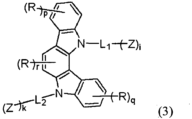


- Eine Verbindung für eine organische Elektrolumineszenzvorrichtung gemäß Anspruch 1, wobei:die Reste R jeweils unabhängig Deuterium, eine Alkylgruppe mit 1 bis 12 Kohlenstoffatomen, eine Aralkylgruppe mit 7 bis 19 Kohlenstoffatomen, eine Alkenylgruppe mit 2 bis 12 Kohlenstoffatomen, eine Alkinylgruppe mit 2 bis 12 Kohlenstoffatomen, eine Dialkylaminogruppe mit 2 bis 24 Kohlenstoffatomen, eine Diarylaminogruppe mit 6 bis 36 Kohlenstoffatomen, eine Diaralkylaminogruppe mit 14 bis 38 Kohlenstoffatomen, eine Acylgruppe mit 2 bis 12 Kohlenstoffatomen, eine Alkoxycarbonylgruppe mit 2 bis 12 Kohlenstoffatomen, eine Alkoxylgruppe mit 1 bis 12 Kohlenstoffatomen, eine Alkylsulfonylgruppe mit 1 bis 12 Kohlenstoffatomen, eine Halogenalkylgruppe mit 1 bis 12 Kohlenstoffatomen, eine Phenoxygruppe, eine Alkylthiogruppe mit 1 bis 12 Kohlenstoffatomen, eine substituierte oder unsubstituierte aromatische Kohlenwasserstoffgruppe mit 6 bis 18 Kohlenstoffatomen, eine substituierte oder unsubstituierte aromatische heterocyclische Gruppe mit 3 bis 17 Kohlenstoffatomen oder eine Bor enthaltende Gruppe, dargestellt durch die Formel (1c), darstellen; undA1 und A2 jeweils unabhängig eine Alkylgruppe mit 1 bis 12 Kohlenstoffatomen, eine substituierte oder unsubstituierte aromatische Kohlenwasserstoffgruppe mit 6 bis 18 Kohlenstoffatomen oder eine substituierte oder unsubstituierte aromatische heterocyclische Gruppe mit 3 bis 17 Kohlenstoffatomen darstellen.
- Eine Verbindung für eine organische Elektrolumineszenzvorrichtung gemäß Anspruch 1, wobei i+k gleich 1 oder mehr ist und die Reste R jeweils eine Gruppe außer einer Bor enthaltenden Gruppe darstellen.
- Eine Verbindung für eine organische Elektrolumineszenzvorrichtung gemäß Anspruch 1, wobei A1 und A2 jeweils unabhängig eine substituierte oder unsubstituierte aromatische Kohlenwasserstoffgruppe mit 6 bis 18 Kohlenstoffatomen oder eine substituierte oder unsubstituierte aromatische heterocyclische Gruppe mit 3 bis 17 Kohlenstoffatomen darstellen.
- Eine organische Elektrolumineszenzvorrichtung, umfassend eine organische Schicht, die eine Verbindung für eine organische Elektrolumineszenzvorrichtung, die durch die folgende allgemeine Formel (1) dargestellt ist, enthält:


 ein Ring I einen aromatischen Kohlenwasserstoffring, dargestellt durch die Formel (1a), darstellt, der an beliebigen Positionen an benachbarte Ringe anelliert werden soll, und ein Ring II einen Heterocyclus, dargestellt durch die Formel (1b), darstellt, der an beliebigen Positionen an benachbarte Ringe anelliert werden soll;L1 und L2 jeweils unabhängig eine i+1-wertige oder k+1-wertige Gruppe darstellen, ausgewählt aus einer substituierten oder unsubstituierten aromatischen Kohlenwasserstoffgruppe mit 6 bis 18 Kohlenstoffatomen, einer substituierten oder unsubstituierten aromatischen heterocyclischen Gruppe mit 3 bis 17 Kohlenstoffatomen, und einer verbundenen aromatischen Gruppe, die durch Verbinden von zwei bis sechs aromatischen Ringen der substituierten oder unsubstituierten aromatischen Kohlenwasserstoffgruppen und der substituierten oder unsubstituierten aromatischen heterocyclischen Gruppen gebildet ist, wobei die verbundene aromatische Gruppe geradkettig oder verzweigt sein kann, und die aromatischen Ringe, die verbunden werden sollen, gleich oder voneinander verschieden sein können;Z eine Bor enthaltende Gruppe mit der Formel (1c) darstellt;die Reste R jeweils unabhängig Deuterium, eine Alkylgruppe mit 1 bis 12 Kohlenstoffatomen, eine Aralkylgruppe mit 7 bis 19 Kohlenstoffatomen, eine Alkenylgruppe mit 2 bis 12 Kohlenstoffatomen, eine Alkinylgruppe mit 2 bis 12 Kohlenstoffatomen, eine Cyanogruppe, eine Dialkylaminogruppe mit 2 bis 24 Kohlenstoffatomen, eine Diarylaminogruppe mit 6 bis 36 Kohlenstoffatomen, eine Diaralkylaminogruppe mit 14 bis 38 Kohlenstoffatomen, eine Aminogruppe, eine Nitrogruppe, eine Acylgruppe mit 2 bis 12 Kohlenstoffatomen, eine Alkoxycarbonylgruppe mit 2 bis 12 Kohlenstoffatomen, eine. Carboxylgruppe, eine Alkoxylgruppe mit 1 bis 12 Kohlenstoffatomen, eine Alkylsulfonylgruppe mit 1 bis 12 Kohlenstoffatomen, eine Halogenalkylgruppe mit 1 bis 12 Kohlenstoffatomen, eine Hydroxylgruppe, eine Amidgruppe, eine Phenoxygruppe, eine Alkylthiogruppe mit 1 bis 12 Kohlenstoffatomen, eine substituierte oder unsubstituierte aromatische Kohlenwasserstoffgruppe mit 6 bis 18 Kohlenstoffatomen, eine substituierte oder unsubstituierte aromatische heterocyclische Gruppe mit 3 bis 17 Kohlenstoffatomen oder eine Bor enthaltende Gruppe, dargestellt durch die Formel (1c), darstellen;A1 und A2 jeweils unabhängig Wasserstoff, Deuterium, eine Alkylgruppe mit 1 bis 12 Kohlenstoffatomen, eine Alkenylgruppe mit 2 bis 12 Kohlenstoffatomen, eine Alkinylgruppe mit 2 bis 12 Kohlenstoffatomen, eine Alkoxylgruppe mit 1 bis 12 Kohlenstoffatomen, eine Hydroxylgruppe, Chlor, Brom, Fluor, eine substituierte oder unsubstituierte aromatische Kohlenwasserstoffgruppe mit 6 bis 18 Kohlenstoffatomen oder eine substituierte oder unsubstituierte aromatische heterocyclische Gruppe mit 3 bis 17 Kohlenstoffatomen darstellen, und A1 und A2 an benachbarte A1 und A2 gebunden sein können oder an Substituenten von A1 und A2 gebunden sein können, um einen Ring zu bilden; undp und q jeweils unabhängig eine ganze Zahl von 0 bis 4 darstellen, r eine ganze Zahl von 0 bis 2 darstellt, und i und k jeweils eine ganze Zahl von 0 bis 5 darstellen, mit der Maßgabe, dass p+q+r+i+k≥1 und wenn i und k beide gleich 0 darstellen, mindestens einer der Reste R eine Bor enthaltende Gruppe, dargestellt durch die Formel (1c), darstellt, und wenn p, q, r, i, und k jeweils 2 oder mehr darstellen, die Reste R und Z gleich oder voneinander verschieden sein können.
 - Eine organische Elektrolumineszenzvorrichtung gemäß Anspruch 6, umfassend eine organische Schicht, die die Verbindung für eine organische Elektrolumineszenzvorrichtung gemäß einem der Ansprüche 1 bis 5 enthält.
- Eine organische Elektrolumineszenzvorrichtung gemäß Anspruch 6 oder 7, wobei die organische Schicht, die die Verbindung für eine organische Elektrolumineszenzvorrichtung enthält, mindestens eine Schicht, ausgewählt aus einer Licht-emittierenden Schicht, einer Lochtransportschicht, einer Lochinjektionsschicht, einer Elektronentransportschicht und einer Elektroneninjektionsschicht umfasst.
- Eine organische Elektrolumineszenzvorrichtung gemäß Anspruch 6 oder 7, wobei die organische Schicht, die die Verbindung für eine organische Elektrolumineszenzvorrichtung enthält, eine Licht-emittierende Schicht umfasst, und die Licht-emittierende Schicht einen phosphoreszenten Licht-emittierenden Dotierstoff und die Verbindung für eine organische Elektrolumineszenzvorrichtung als ein Gastmaterial enthält.
Applications Claiming Priority (2)
| Application Number | Priority Date | Filing Date | Title |
|---|---|---|---|
| JP2012216564 | 2012-09-28 | ||
| PCT/JP2013/075937 WO2014050904A1 (ja) | 2012-09-28 | 2013-09-25 | 有機電界発光素子用化合物及び有機電界発光素子 |
Publications (3)
| Publication Number | Publication Date |
|---|---|
| EP2903048A1 EP2903048A1 (de) | 2015-08-05 |
| EP2903048A4 EP2903048A4 (de) | 2016-05-18 |
| EP2903048B1 true EP2903048B1 (de) | 2018-01-10 |
Family
ID=50388299
Family Applications (1)
| Application Number | Title | Priority Date | Filing Date |
|---|---|---|---|
| EP13841725.8A Not-in-force EP2903048B1 (de) | 2012-09-28 | 2013-09-25 | Verbindung für organische elektrolumineszenzelemente und organisches elektrolumineszenzelement |
Country Status (7)
| Country | Link |
|---|---|
| US (1) | US20150218191A1 (de) |
| EP (1) | EP2903048B1 (de) |
| JP (1) | JP6334404B2 (de) |
| KR (1) | KR102097718B1 (de) |
| CN (1) | CN104662688B (de) |
| TW (1) | TWI599570B (de) |
| WO (1) | WO2014050904A1 (de) |
Families Citing this family (16)
| Publication number | Priority date | Publication date | Assignee | Title |
|---|---|---|---|---|
| CN107325050A (zh) | 2012-12-28 | 2017-11-07 | 出光兴产株式会社 | 有机电致发光元件 |
| US11895909B2 (en) * | 2015-04-29 | 2024-02-06 | Samsung Display Co., Ltd. | Organic light-emitting device |
| EP3188260B1 (de) * | 2015-12-31 | 2020-02-12 | Dow Global Technologies Llc | Nanostrukturmaterialstrukturen und verfahren |
| JP6803727B2 (ja) * | 2016-09-23 | 2020-12-23 | 日本放送協会 | 有機エレクトロルミネッセンス素子 |
| KR102109545B1 (ko) | 2016-12-22 | 2020-05-12 | 삼성에스디아이 주식회사 | 유기 광전자 소자용 조성물, 유기 광전자 소자 및 표시 장치 |
| JP6883437B2 (ja) * | 2017-01-31 | 2021-06-09 | 日本放送協会 | 有機エレクトロルミネッセンス素子 |
| US10892425B1 (en) * | 2017-03-03 | 2021-01-12 | Kyulux, Inc. | Composition of matter for use in organic light-emitting diodes |
| JP6846256B2 (ja) * | 2017-03-29 | 2021-03-24 | 日鉄ケミカル&マテリアル株式会社 | 有機電界発光素子用材料及びこれを用いた有機電界発光素子 |
| JP6846258B2 (ja) * | 2017-03-29 | 2021-03-24 | 日鉄ケミカル&マテリアル株式会社 | 有機電界発光素子用材料及びこれを用いた有機電界発光素子 |
| CN111094385B (zh) * | 2017-09-22 | 2024-04-09 | 三菱化学株式会社 | 电荷传输性化合物、含有电荷传输性化合物的组合物和使用该组合物的有机电致发光元件 |
| KR102595754B1 (ko) * | 2018-08-09 | 2023-10-30 | 덕산네오룩스 주식회사 | 이종 화합물의 혼합물을 호스트로 포함하는 유기전기소자 및 그 전자 장치 |
| WO2020111602A1 (ko) | 2018-11-27 | 2020-06-04 | 주식회사 엘지화학 | 신규한 화합물 및 이를 포함하는 유기발광 소자 |
| CN109678861A (zh) * | 2018-12-31 | 2019-04-26 | 瑞声科技(南京)有限公司 | 一种双极性热激活延迟荧光化合物及其应用 |
| CN109705125A (zh) * | 2018-12-31 | 2019-05-03 | 瑞声科技(南京)有限公司 | 一种双极性热延迟荧光化合物及其应用 |
| KR20210136224A (ko) | 2020-05-06 | 2021-11-17 | 삼성디스플레이 주식회사 | 발광 소자 및 이를 포함하는 전자 장치 |
| EP4180500A1 (de) | 2020-07-08 | 2023-05-17 | NIPPON STEEL Chemical & Material Co., Ltd. | Wärmeaktiviertes verzögertes fluoreszenzmaterial und organisches elektrolumineszenzelement |
Family Cites Families (112)
| Publication number | Priority date | Publication date | Assignee | Title |
|---|---|---|---|---|
| US5942340A (en) | 1997-10-02 | 1999-08-24 | Xerox Corporation | Indolocarbazole electroluminescent devices |
| US5952115A (en) | 1997-10-02 | 1999-09-14 | Xerox Corporation | Electroluminescent devices |
| ATE511222T1 (de) | 1999-12-01 | 2011-06-15 | Univ Princeton | Komplex der formel l2irx |
| JP2001313178A (ja) | 2000-04-28 | 2001-11-09 | Pioneer Electronic Corp | 有機エレクトロルミネッセンス素子 |
| JP4340401B2 (ja) | 2000-07-17 | 2009-10-07 | 富士フイルム株式会社 | 発光素子及びイリジウム錯体 |
| CN100505375C (zh) | 2000-08-11 | 2009-06-24 | 普林斯顿大学理事会 | 有机金属化合物和发射转换有机电致磷光 |
| US6939624B2 (en) | 2000-08-11 | 2005-09-06 | Universal Display Corporation | Organometallic compounds and emission-shifting organic electrophosphorescence |
| EP1217668A1 (de) * | 2000-12-22 | 2002-06-26 | Covion Organic Semiconductors GmbH | Verwendung von Bor- und Aluminium-Verbindungen in Elektronik-Bauteilen |
| JP3812730B2 (ja) | 2001-02-01 | 2006-08-23 | 富士写真フイルム株式会社 | 遷移金属錯体及び発光素子 |
| JP4285947B2 (ja) | 2001-06-15 | 2009-06-24 | 三洋電機株式会社 | 発光性有機金属化合物及び発光素子 |
| JP2003123982A (ja) | 2001-08-07 | 2003-04-25 | Fuji Photo Film Co Ltd | 発光素子及び新規イリジウム錯体 |
| JP2003073387A (ja) | 2001-09-04 | 2003-03-12 | Canon Inc | 金属配位化合物及び有機発光素子 |
| US6835473B2 (en) * | 2001-12-06 | 2004-12-28 | Konica Corporation | Organic electroluminescence element and display |
| JP2003253128A (ja) | 2002-02-28 | 2003-09-10 | Jsr Corp | 発光性組成物 |
| JP2003253129A (ja) | 2002-02-28 | 2003-09-10 | Jsr Corp | 発光性組成物 |
| JP2003253145A (ja) | 2002-02-28 | 2003-09-10 | Jsr Corp | 発光性組成物 |
| JP3969132B2 (ja) | 2002-03-12 | 2007-09-05 | コニカミノルタホールディングス株式会社 | 有機エレクトロルミネッセンス素子及びそれを用いた表示装置 |
| WO2004016711A1 (en) | 2002-08-16 | 2004-02-26 | The University Of Southern California | Organic light emitting materials and devices |
| US6916554B2 (en) | 2002-11-06 | 2005-07-12 | The University Of Southern California | Organic light emitting materials and devices |
| JP2004111193A (ja) | 2002-09-18 | 2004-04-08 | Konica Minolta Holdings Inc | 有機エレクトロルミネッセンス素子及び表示装置 |
| US20040086743A1 (en) | 2002-11-06 | 2004-05-06 | Brown Cory S. | Organometallic compounds for use in electroluminescent devices |
| JP4218311B2 (ja) | 2002-11-06 | 2009-02-04 | 株式会社豊田中央研究所 | 有機金属錯体化合物及びこれを用いた有機発光素子 |
| US6858327B2 (en) | 2002-11-08 | 2005-02-22 | Universal Display Corporation | Organic light emitting materials and devices |
| JP2004319438A (ja) | 2003-03-28 | 2004-11-11 | Konica Minolta Holdings Inc | 有機エレクトロルミネッセンス素子、表示装置、照明装置及びロジウム錯体化合物 |
| KR100682858B1 (ko) | 2003-06-26 | 2007-02-15 | 삼성에스디아이 주식회사 | 유기 금속 착물 및 이를 채용한 유기 전계 발광 소자 |
| KR100718100B1 (ko) | 2003-09-06 | 2007-05-14 | 삼성에스디아이 주식회사 | 이핵 유기금속 착물 및 이를 이용한 유기 전계 발광 소자 |
| KR100773523B1 (ko) | 2003-11-06 | 2007-11-07 | 삼성에스디아이 주식회사 | 유기 금속 착물 및 이를 이용한 유기 전계 발광 소자 |
| KR100773524B1 (ko) | 2003-12-24 | 2007-11-07 | 삼성에스디아이 주식회사 | 이핵 유기 금속 착물 및 이를 이용한 유기 전계 발광 소자 |
| US7279232B2 (en) | 2004-01-26 | 2007-10-09 | Universal Display Corporation | Electroluminescent stability |
| KR100537621B1 (ko) | 2004-02-02 | 2005-12-19 | 삼성에스디아이 주식회사 | 이리듐 화합물 및 이를 이용한 유기 전계 발광 소자 |
| US7332232B2 (en) | 2004-02-03 | 2008-02-19 | Universal Display Corporation | OLEDs utilizing multidentate ligand systems |
| WO2005113704A2 (en) | 2004-05-18 | 2005-12-01 | The University Of Southern California | Luminescent compounds with carbene ligands |
| US7534505B2 (en) | 2004-05-18 | 2009-05-19 | The University Of Southern California | Organometallic compounds for use in electroluminescent devices |
| US7279704B2 (en) | 2004-05-18 | 2007-10-09 | The University Of Southern California | Complexes with tridentate ligands |
| US20060008670A1 (en) | 2004-07-06 | 2006-01-12 | Chun Lin | Organic light emitting materials and devices |
| JP4574470B2 (ja) | 2004-07-06 | 2010-11-04 | キヤノン株式会社 | データ処理装置およびディザパターン製造方法 |
| EP3428986B1 (de) | 2004-07-07 | 2021-01-20 | Universal Display Corporation | Stabile und leistungsstarke elektrolumineszente materialien |
| KR101030011B1 (ko) | 2004-08-28 | 2011-04-20 | 삼성모바일디스플레이주식회사 | 시클로메탈화 전이금속 착물 및 이를 이용한 유기 전계발광 소자 |
| JP4500735B2 (ja) | 2004-09-22 | 2010-07-14 | 富士フイルム株式会社 | 有機電界発光素子 |
| JP4531509B2 (ja) | 2004-09-27 | 2010-08-25 | 富士フイルム株式会社 | 発光素子 |
| KR100668305B1 (ko) | 2004-10-01 | 2007-01-12 | 삼성에스디아이 주식회사 | 시클로메탈화 전이금속 착물 및 이를 이용한 유기 전계발광 소자 |
| JP4687059B2 (ja) | 2004-10-06 | 2011-05-25 | 凸版印刷株式会社 | 有機金属錯体、および発光材料、並びに発光素子 |
| KR101015882B1 (ko) | 2004-10-11 | 2011-02-23 | 삼성모바일디스플레이주식회사 | 시클로메탈화 전이금속 착물 및 이를 이용한 유기 전계발광 소자 |
| JP5243684B2 (ja) | 2004-11-04 | 2013-07-24 | ユー・ディー・シー アイルランド リミテッド | 有機金属錯体、発光性固体、有機el素子及び有機elディスプレイ |
| JP2006131561A (ja) | 2004-11-08 | 2006-05-25 | Idemitsu Kosan Co Ltd | 金属錯体化合物 |
| KR101234226B1 (ko) | 2005-02-03 | 2013-02-18 | 삼성디스플레이 주식회사 | 유기 금속 착물 및 이를 이용한 유기 전계 발광 소자 |
| JPWO2006100888A1 (ja) | 2005-03-22 | 2008-08-28 | コニカミノルタホールディングス株式会社 | 有機el素子用材料、有機el素子、表示装置及び照明装置 |
| KR101223717B1 (ko) | 2005-04-12 | 2013-01-18 | 삼성디스플레이 주식회사 | 실릴 치환된 시클로메탈화 전이금속 착물 및 이를 이용한 유기 전계 발광 소자 |
| KR100611885B1 (ko) | 2005-04-21 | 2006-08-11 | 삼성에스디아이 주식회사 | 호스트용 화합물과 도판트용 화합물이 연결된 유기 금속화합물, 이를 이용한 유기 전계 발광 소자 및 그의제조방법 |
| KR100732823B1 (ko) | 2005-04-21 | 2007-06-27 | 삼성에스디아이 주식회사 | 호스트용 화합물과 도판트용 화합물이 연결된 유기 금속화합물, 이를 이용한 유기 전계 발광 소자 및 그의제조방법 |
| JP4801928B2 (ja) | 2005-04-25 | 2011-10-26 | 富士フイルム株式会社 | 有機電界発光素子 |
| JP2006303394A (ja) | 2005-04-25 | 2006-11-02 | Fuji Photo Film Co Ltd | 有機電界発光素子 |
| JP2006310479A (ja) | 2005-04-27 | 2006-11-09 | Fuji Photo Film Co Ltd | 有機電界発光素子 |
| US7902374B2 (en) | 2005-05-06 | 2011-03-08 | Universal Display Corporation | Stability OLED materials and devices |
| US9051344B2 (en) | 2005-05-06 | 2015-06-09 | Universal Display Corporation | Stability OLED materials and devices |
| JP4904727B2 (ja) | 2005-06-23 | 2012-03-28 | コニカミノルタホールディングス株式会社 | 有機エレクトロルミネッセンス素子材料、有機エレクトロルミネッセンス素子、表示装置及び照明装置 |
| JP4935001B2 (ja) | 2005-06-29 | 2012-05-23 | コニカミノルタホールディングス株式会社 | 有機エレクトロルミネッセンス素子材料 |
| US20090039771A1 (en) | 2005-07-01 | 2009-02-12 | Konica Minolta Holdings, Inc. | Organic electroluminescent element material, organic electroluminescent element, display device and lighting device |
| KR20080037006A (ko) | 2005-08-05 | 2008-04-29 | 이데미쓰 고산 가부시키가이샤 | 전이금속 착체화합물 및 그것을 이용한 유기 전기발광 소자 |
| WO2007023659A1 (ja) | 2005-08-25 | 2007-03-01 | Konica Minolta Holdings, Inc. | 有機エレクトロルミネッセンス素子材料、有機エレクトロルミネッセンス素子、表示装置及び照明装置 |
| JP4867244B2 (ja) * | 2005-09-12 | 2012-02-01 | Jsr株式会社 | 電荷輸送性化合物およびその製造方法、有機エレクトロルミネッセンス素子用組成物並びに有機エレクトロルミネッセンス素子 |
| JP2007088105A (ja) | 2005-09-20 | 2007-04-05 | Fujifilm Corp | 有機電界発光素子 |
| JPWO2007058080A1 (ja) | 2005-11-17 | 2009-04-30 | 出光興産株式会社 | 金属錯体化合物及びそれを用いた有機エレクトロルミネッセンス素子 |
| WO2007058104A1 (ja) | 2005-11-17 | 2007-05-24 | Idemitsu Kosan Co., Ltd. | 金属錯体化合物及びそれを用いた有機エレクトロルミネッセンス素子 |
| CN101415718B (zh) | 2006-02-10 | 2013-05-29 | 通用显示公司 | 环金属化的咪唑并[1,2-f]菲啶和二咪唑并[1,2-a:1',2'-c]喹唑啉配位体和其等电子和苯并环化类似物的金属络合物 |
| JP4945156B2 (ja) | 2006-03-24 | 2012-06-06 | 富士フイルム株式会社 | 有機電界発光素子 |
| EP1842854A1 (de) | 2006-04-07 | 2007-10-10 | SOLVAY (Société Anonyme) | Lichtemittierendes Material |
| US7737277B2 (en) | 2006-05-08 | 2010-06-15 | E.I. Du Pont De Nemours And Company | Electroluminescent bis-cyclometalled iridium compounds and devices made with such compounds |
| JP5144034B2 (ja) | 2006-05-31 | 2013-02-13 | 富士フイルム株式会社 | 有機電界発光素子 |
| ATE449830T1 (de) | 2006-06-26 | 2009-12-15 | Basf Se | Verwendung von pt- und pd-bis- und tetracarbenkomplexen mit verbrückten carbenliganden in oleds |
| JP2008037848A (ja) | 2006-08-10 | 2008-02-21 | Takasago Internatl Corp | 白金錯体及び発光素子 |
| JP5644050B2 (ja) | 2006-09-20 | 2014-12-24 | コニカミノルタ株式会社 | 有機エレクトロルミネッセンス素子材料 |
| WO2008050733A1 (fr) | 2006-10-24 | 2008-05-02 | Ube Industries, Ltd. | Complexe de l'or, procédé pour la production du complexe de l'or et élément électroluminescent ultraviolet organique utilisant le complexe de l'or |
| CN101511834B (zh) | 2006-11-09 | 2013-03-27 | 新日铁化学株式会社 | 有机场致发光元件用化合物及有机场致发光元件 |
| JP5127206B2 (ja) | 2006-11-28 | 2013-01-23 | キヤノン株式会社 | 金属錯体化合物、有機発光素子及び表示装置 |
| US8778508B2 (en) | 2006-12-08 | 2014-07-15 | Universal Display Corporation | Light-emitting organometallic complexes |
| EP3719099B1 (de) | 2007-03-08 | 2022-09-14 | Universal Display Corporation | Phosphoreszierende materialien |
| JP2008270737A (ja) | 2007-03-23 | 2008-11-06 | Fujifilm Corp | 有機電界発光素子 |
| JP2008239565A (ja) | 2007-03-28 | 2008-10-09 | Idemitsu Kosan Co Ltd | イリジウム錯体とその製造法及びそれを用いた有機エレクトロルミネッセンス |
| JP5202864B2 (ja) | 2007-03-29 | 2013-06-05 | コニカミノルタホールディングス株式会社 | 有機エレクトロルミネッセンス素子及びそれを用いた表示装置 |
| JP2008266163A (ja) | 2007-04-17 | 2008-11-06 | Idemitsu Kosan Co Ltd | 遷移金属錯体化合物及びそれを用いた有機エレクトロルミネッセンス素子 |
| US7993763B2 (en) | 2007-05-10 | 2011-08-09 | Universal Display Corporation | Organometallic compounds having host and dopant functionalities |
| JP5256485B2 (ja) | 2007-05-16 | 2013-08-07 | コニカミノルタ株式会社 | 有機エレクトロルミネッセンス素子、表示装置及び照明装置 |
| TWI468489B (zh) | 2007-05-29 | 2015-01-11 | Nippon Steel & Sumikin Chem Co | Organic electroluminescent element compounds and organic electroluminescent elements |
| US8013330B2 (en) * | 2007-05-30 | 2011-09-06 | Nippon Steel Chemical Co., Ltd | Compound for organic electroluminescent device and organic electroluminescent device |
| WO2008156879A1 (en) | 2007-06-20 | 2008-12-24 | Universal Display Corporation | Blue phosphorescent imidazophenanthridine materials |
| JP5088025B2 (ja) | 2007-07-12 | 2012-12-05 | コニカミノルタホールディングス株式会社 | 有機エレクトロルミネッセンス材料、有機エレクトロルミネッセンス素子、表示装置及び照明装置 |
| JP2009057367A (ja) | 2007-08-03 | 2009-03-19 | Idemitsu Kosan Co Ltd | 金属錯体化合物、有機エレクトロルミネッセンス素子用材料及びそれを用いた有機エレクトロルミネッセンス素子 |
| JP5115094B2 (ja) | 2007-08-21 | 2013-01-09 | コニカミノルタホールディングス株式会社 | 有機エレクトロルミネッセンス素子材料、有機エレクトロルミネッセンス素子、表示装置及び照明装置 |
| JP2009057304A (ja) | 2007-08-30 | 2009-03-19 | Mitsubishi Chemicals Corp | 金属錯体及び有機電界発光素子 |
| JP5438941B2 (ja) | 2007-09-25 | 2014-03-12 | ユー・ディー・シー アイルランド リミテッド | 有機電界発光素子 |
| JP4816610B2 (ja) | 2007-09-26 | 2011-11-16 | コニカミノルタホールディングス株式会社 | 有機エレクトロルミネッセンス素子 |
| US8067100B2 (en) | 2007-10-04 | 2011-11-29 | Universal Display Corporation | Complexes with tridentate ligands |
| JP2009114369A (ja) | 2007-11-08 | 2009-05-28 | Konica Minolta Holdings Inc | 有機エレクトロルミネッセンス材料、有機エレクトロルミネッセンス素子、表示装置及び照明装置 |
| JP5438955B2 (ja) | 2007-12-14 | 2014-03-12 | ユー・ディー・シー アイルランド リミテッド | 白金錯体化合物及びこれを用いた有機電界発光素子 |
| KR101082144B1 (ko) * | 2008-05-08 | 2011-11-09 | 신닛테츠가가쿠 가부시키가이샤 | 유기 전계 발광 소자용 화합물 및 유기 전계 발광 소자 |
| JP2009286716A (ja) | 2008-05-28 | 2009-12-10 | Sumitomo Seika Chem Co Ltd | イリジウム錯体 |
| JP2010083852A (ja) | 2008-10-03 | 2010-04-15 | Wakayama Univ | 金属錯体の製造方法、金属錯体および有機電界発光素子 |
| KR101477613B1 (ko) | 2009-03-31 | 2014-12-30 | 롬엔드하스전자재료코리아유한회사 | 신규한 유기 전자재료용 화합물 및 이를 포함하는 유기 전자 소자 |
| TWI471406B (zh) * | 2009-03-31 | 2015-02-01 | Nippon Steel & Sumikin Chem Co | A phosphorescent element, and an organic electroluminescent device using the same |
| KR101801048B1 (ko) * | 2009-06-08 | 2017-11-28 | 에스에프씨 주식회사 | 인돌로카바졸 유도체 및 이를 이용한 유기전계발광소자 |
| KR101902917B1 (ko) * | 2009-07-27 | 2018-10-02 | 에스에프씨 주식회사 | 인돌로카바졸 유도체 및 이를 이용한 유기전계발광소자 |
| KR101324788B1 (ko) * | 2009-12-31 | 2013-10-31 | (주)씨에스엘쏠라 | 유기 광소자 및 이를 위한 유기 광합물 |
| JP2011213643A (ja) | 2010-03-31 | 2011-10-27 | Canon Inc | 銅錯体化合物及びこれを用いた有機発光素子 |
| JP5931051B2 (ja) * | 2010-04-06 | 2016-06-08 | ビーエーエスエフ ソシエタス・ヨーロピアBasf Se | 置換カルバゾール誘導体および有機エレクトロニクスにおけるその使用 |
| WO2012039561A1 (en) * | 2010-09-20 | 2012-03-29 | Rohm And Haas Electronic Materials Korea Ltd. | Novel organic electroluminescent compounds and organic electroluminescent device using the same |
| KR101256205B1 (ko) * | 2010-09-30 | 2013-04-19 | (주)씨에스엘쏠라 | 유기발광화합물 및 이를 구비한 유기발광소자 |
| KR20120052879A (ko) * | 2010-11-16 | 2012-05-24 | 롬엔드하스전자재료코리아유한회사 | 신규한 유기 전자재료용 화합물 및 이를 채용하고 있는 유기 전계 발광 소자 |
| JP2012140367A (ja) * | 2010-12-28 | 2012-07-26 | Idemitsu Kosan Co Ltd | 縮合多環化合物、有機エレクトロルミネッセンス素子用材料、及びそれを用いた有機エレクトロルミネッセンス素子 |
| CN103688383B (zh) * | 2011-06-27 | 2016-01-20 | 新日铁住金化学株式会社 | 有机电致发光元件用聚合物及使用了其的有机电致发光元件 |
| WO2013088934A1 (ja) * | 2011-12-12 | 2013-06-20 | 新日鉄住金化学株式会社 | 有機電界発光素子用材料及びそれを用いた有機電界発光素子 |
| CN102827196B (zh) * | 2012-09-12 | 2015-06-03 | 山西大学 | 一种含硼吲哚[3,2-b]咔唑衍生物及其制备方法和应用 |
-
2013
- 2013-09-18 TW TW102133877A patent/TWI599570B/zh not_active IP Right Cessation
- 2013-09-25 EP EP13841725.8A patent/EP2903048B1/de not_active Not-in-force
- 2013-09-25 WO PCT/JP2013/075937 patent/WO2014050904A1/ja active Application Filing
- 2013-09-25 JP JP2014538540A patent/JP6334404B2/ja not_active Expired - Fee Related
- 2013-09-25 KR KR1020157010556A patent/KR102097718B1/ko active IP Right Grant
- 2013-09-25 US US14/421,792 patent/US20150218191A1/en not_active Abandoned
- 2013-09-25 CN CN201380050369.7A patent/CN104662688B/zh not_active Expired - Fee Related
Non-Patent Citations (1)
| Title |
|---|
| None * |
Also Published As
| Publication number | Publication date |
|---|---|
| KR102097718B1 (ko) | 2020-04-07 |
| WO2014050904A1 (ja) | 2014-04-03 |
| TWI599570B (zh) | 2017-09-21 |
| KR20150063462A (ko) | 2015-06-09 |
| CN104662688A (zh) | 2015-05-27 |
| EP2903048A1 (de) | 2015-08-05 |
| TW201431864A (zh) | 2014-08-16 |
| EP2903048A4 (de) | 2016-05-18 |
| US20150218191A1 (en) | 2015-08-06 |
| CN104662688B (zh) | 2017-06-23 |
| JP6334404B2 (ja) | 2018-05-30 |
| JPWO2014050904A1 (ja) | 2016-08-22 |
Similar Documents
| Publication | Publication Date | Title |
|---|---|---|
| EP2903048B1 (de) | Verbindung für organische elektrolumineszenzelemente und organisches elektrolumineszenzelement | |
| EP2985802B1 (de) | Adamantanverbindung für organische elektrolumineszenzelemente und organisches elektrolumineszenzelement | |
| EP2827397B1 (de) | Organisches elektrolumineszenzelement | |
| EP2793280B1 (de) | Material für ein organisches elektrolumineszentes element und organisches elektrolumineszentes element, das dieses verwendet | |
| EP2869356B1 (de) | Organisches elektrolumineszierendes element und material für ein organisches elektrolumineszierendes element | |
| EP3054496B1 (de) | Material für ein organisches elektrolumineszierendes element und organisches elektrolumineszierendes element damit | |
| EP2629345B1 (de) | Organisches elektrolumineszenzelement | |
| EP3089230B1 (de) | Material für organische elektrolumineszierende elemente und organisches elektrolumineszierendes element daraus | |
| EP3125326B1 (de) | Material für ein organisches elektrolumineszentes element und organische elektrolumineszente elemente damit | |
| US9716238B2 (en) | Boron compound for organic electroluminescent elements, and organic electroluminescent element | |
| EP3054495B1 (de) | Material für organische elektrolumineszenzelemente und dieses verwendetes organisches elektrolumineszenzelement | |
| EP2876699B1 (de) | Organisches elektrolumineszenzelement | |
| EP3279964A1 (de) | Material für ein organisches elektrolumineszenzelement und organisches elektrolumineszenzelement damit | |
| EP3125325B1 (de) | Material für ein organisches elektrolumineszenzelement und ein organisches elektrolumineszenzelement in dem es verwendet wird | |
| EP3125324B1 (de) | Material für ein organisches elektrolumineszentes element und organisches elektrolumineszentes element damit | |
| EP3089231B1 (de) | Material für organische elektrolumineszierende elemente und organisches elektrolumineszierendes element damit | |
| EP3279962B1 (de) | Material für ein organisches elektrolumineszierendes element und organisches elektrolumineszierendes element damit |
Legal Events
| Date | Code | Title | Description |
|---|---|---|---|
| PUAI | Public reference made under article 153(3) epc to a published international application that has entered the european phase |
Free format text: ORIGINAL CODE: 0009012 |
|
| 17P | Request for examination filed |
Effective date: 20150411 |
|
| AK | Designated contracting states |
Kind code of ref document: A1 Designated state(s): AL AT BE BG CH CY CZ DE DK EE ES FI FR GB GR HR HU IE IS IT LI LT LU LV MC MK MT NL NO PL PT RO RS SE SI SK SM TR |
|
| AX | Request for extension of the european patent |
Extension state: BA ME |
|
| DAX | Request for extension of the european patent (deleted) | ||
| RA4 | Supplementary search report drawn up and despatched (corrected) |
Effective date: 20160420 |
|
| RIC1 | Information provided on ipc code assigned before grant |
Ipc: H01L 51/50 20060101AFI20160413BHEP Ipc: C07F 5/02 20060101ALI20160413BHEP Ipc: C09K 11/06 20060101ALI20160413BHEP |
|
| GRAP | Despatch of communication of intention to grant a patent |
Free format text: ORIGINAL CODE: EPIDOSNIGR1 |
|
| INTG | Intention to grant announced |
Effective date: 20170412 |
|
| GRAS | Grant fee paid |
Free format text: ORIGINAL CODE: EPIDOSNIGR3 |
|
| GRAJ | Information related to disapproval of communication of intention to grant by the applicant or resumption of examination proceedings by the epo deleted |
Free format text: ORIGINAL CODE: EPIDOSDIGR1 |
|
| GRAL | Information related to payment of fee for publishing/printing deleted |
Free format text: ORIGINAL CODE: EPIDOSDIGR3 |
|
| GRAP | Despatch of communication of intention to grant a patent |
Free format text: ORIGINAL CODE: EPIDOSNIGR1 |
|
| INTC | Intention to grant announced (deleted) | ||
| INTG | Intention to grant announced |
Effective date: 20171005 |
|
| GRAA | (expected) grant |
Free format text: ORIGINAL CODE: 0009210 |
|
| AK | Designated contracting states |
Kind code of ref document: B1 Designated state(s): AL AT BE BG CH CY CZ DE DK EE ES FI FR GB GR HR HU IE IS IT LI LT LU LV MC MK MT NL NO PL PT RO RS SE SI SK SM TR |
|
| REG | Reference to a national code |
Ref country code: CH Ref legal event code: EP Ref country code: AT Ref legal event code: REF Ref document number: 963316 Country of ref document: AT Kind code of ref document: T Effective date: 20180115 |
|
| REG | Reference to a national code |
Ref country code: IE Ref legal event code: FG4D |
|
| REG | Reference to a national code |
Ref country code: DE Ref legal event code: R096 Ref document number: 602013031982 Country of ref document: DE |
|
| REG | Reference to a national code |
Ref country code: NL Ref legal event code: MP Effective date: 20180110 |
|
| REG | Reference to a national code |
Ref country code: AT Ref legal event code: MK05 Ref document number: 963316 Country of ref document: AT Kind code of ref document: T Effective date: 20180110 |
|
| PG25 | Lapsed in a contracting state [announced via postgrant information from national office to epo] |
Ref country code: NL Free format text: LAPSE BECAUSE OF FAILURE TO SUBMIT A TRANSLATION OF THE DESCRIPTION OR TO PAY THE FEE WITHIN THE PRESCRIBED TIME-LIMIT Effective date: 20180110 |
|
| PG25 | Lapsed in a contracting state [announced via postgrant information from national office to epo] |
Ref country code: ES Free format text: LAPSE BECAUSE OF FAILURE TO SUBMIT A TRANSLATION OF THE DESCRIPTION OR TO PAY THE FEE WITHIN THE PRESCRIBED TIME-LIMIT Effective date: 20180110 Ref country code: NO Free format text: LAPSE BECAUSE OF FAILURE TO SUBMIT A TRANSLATION OF THE DESCRIPTION OR TO PAY THE FEE WITHIN THE PRESCRIBED TIME-LIMIT Effective date: 20180410 Ref country code: FI Free format text: LAPSE BECAUSE OF FAILURE TO SUBMIT A TRANSLATION OF THE DESCRIPTION OR TO PAY THE FEE WITHIN THE PRESCRIBED TIME-LIMIT Effective date: 20180110 Ref country code: LT Free format text: LAPSE BECAUSE OF FAILURE TO SUBMIT A TRANSLATION OF THE DESCRIPTION OR TO PAY THE FEE WITHIN THE PRESCRIBED TIME-LIMIT Effective date: 20180110 Ref country code: CY Free format text: LAPSE BECAUSE OF FAILURE TO SUBMIT A TRANSLATION OF THE DESCRIPTION OR TO PAY THE FEE WITHIN THE PRESCRIBED TIME-LIMIT Effective date: 20180110 Ref country code: HR Free format text: LAPSE BECAUSE OF FAILURE TO SUBMIT A TRANSLATION OF THE DESCRIPTION OR TO PAY THE FEE WITHIN THE PRESCRIBED TIME-LIMIT Effective date: 20180110 |
|
| PG25 | Lapsed in a contracting state [announced via postgrant information from national office to epo] |
Ref country code: RS Free format text: LAPSE BECAUSE OF FAILURE TO SUBMIT A TRANSLATION OF THE DESCRIPTION OR TO PAY THE FEE WITHIN THE PRESCRIBED TIME-LIMIT Effective date: 20180110 Ref country code: AT Free format text: LAPSE BECAUSE OF FAILURE TO SUBMIT A TRANSLATION OF THE DESCRIPTION OR TO PAY THE FEE WITHIN THE PRESCRIBED TIME-LIMIT Effective date: 20180110 Ref country code: PL Free format text: LAPSE BECAUSE OF FAILURE TO SUBMIT A TRANSLATION OF THE DESCRIPTION OR TO PAY THE FEE WITHIN THE PRESCRIBED TIME-LIMIT Effective date: 20180110 Ref country code: LV Free format text: LAPSE BECAUSE OF FAILURE TO SUBMIT A TRANSLATION OF THE DESCRIPTION OR TO PAY THE FEE WITHIN THE PRESCRIBED TIME-LIMIT Effective date: 20180110 Ref country code: BG Free format text: LAPSE BECAUSE OF FAILURE TO SUBMIT A TRANSLATION OF THE DESCRIPTION OR TO PAY THE FEE WITHIN THE PRESCRIBED TIME-LIMIT Effective date: 20180410 Ref country code: GR Free format text: LAPSE BECAUSE OF FAILURE TO SUBMIT A TRANSLATION OF THE DESCRIPTION OR TO PAY THE FEE WITHIN THE PRESCRIBED TIME-LIMIT Effective date: 20180411 Ref country code: IS Free format text: LAPSE BECAUSE OF FAILURE TO SUBMIT A TRANSLATION OF THE DESCRIPTION OR TO PAY THE FEE WITHIN THE PRESCRIBED TIME-LIMIT Effective date: 20180510 Ref country code: SE Free format text: LAPSE BECAUSE OF FAILURE TO SUBMIT A TRANSLATION OF THE DESCRIPTION OR TO PAY THE FEE WITHIN THE PRESCRIBED TIME-LIMIT Effective date: 20180110 |
|
| REG | Reference to a national code |
Ref country code: DE Ref legal event code: R097 Ref document number: 602013031982 Country of ref document: DE |
|
| PG25 | Lapsed in a contracting state [announced via postgrant information from national office to epo] |
Ref country code: RO Free format text: LAPSE BECAUSE OF FAILURE TO SUBMIT A TRANSLATION OF THE DESCRIPTION OR TO PAY THE FEE WITHIN THE PRESCRIBED TIME-LIMIT Effective date: 20180110 Ref country code: AL Free format text: LAPSE BECAUSE OF FAILURE TO SUBMIT A TRANSLATION OF THE DESCRIPTION OR TO PAY THE FEE WITHIN THE PRESCRIBED TIME-LIMIT Effective date: 20180110 Ref country code: EE Free format text: LAPSE BECAUSE OF FAILURE TO SUBMIT A TRANSLATION OF THE DESCRIPTION OR TO PAY THE FEE WITHIN THE PRESCRIBED TIME-LIMIT Effective date: 20180110 Ref country code: IT Free format text: LAPSE BECAUSE OF FAILURE TO SUBMIT A TRANSLATION OF THE DESCRIPTION OR TO PAY THE FEE WITHIN THE PRESCRIBED TIME-LIMIT Effective date: 20180110 |
|
| PLBE | No opposition filed within time limit |
Free format text: ORIGINAL CODE: 0009261 |
|
| STAA | Information on the status of an ep patent application or granted ep patent |
Free format text: STATUS: NO OPPOSITION FILED WITHIN TIME LIMIT |
|
| PG25 | Lapsed in a contracting state [announced via postgrant information from national office to epo] |
Ref country code: DK Free format text: LAPSE BECAUSE OF FAILURE TO SUBMIT A TRANSLATION OF THE DESCRIPTION OR TO PAY THE FEE WITHIN THE PRESCRIBED TIME-LIMIT Effective date: 20180110 Ref country code: SM Free format text: LAPSE BECAUSE OF FAILURE TO SUBMIT A TRANSLATION OF THE DESCRIPTION OR TO PAY THE FEE WITHIN THE PRESCRIBED TIME-LIMIT Effective date: 20180110 Ref country code: SK Free format text: LAPSE BECAUSE OF FAILURE TO SUBMIT A TRANSLATION OF THE DESCRIPTION OR TO PAY THE FEE WITHIN THE PRESCRIBED TIME-LIMIT Effective date: 20180110 Ref country code: CZ Free format text: LAPSE BECAUSE OF FAILURE TO SUBMIT A TRANSLATION OF THE DESCRIPTION OR TO PAY THE FEE WITHIN THE PRESCRIBED TIME-LIMIT Effective date: 20180110 |
|
| 26N | No opposition filed |
Effective date: 20181011 |
|
| PG25 | Lapsed in a contracting state [announced via postgrant information from national office to epo] |
Ref country code: SI Free format text: LAPSE BECAUSE OF FAILURE TO SUBMIT A TRANSLATION OF THE DESCRIPTION OR TO PAY THE FEE WITHIN THE PRESCRIBED TIME-LIMIT Effective date: 20180110 |
|
| PG25 | Lapsed in a contracting state [announced via postgrant information from national office to epo] |
Ref country code: MC Free format text: LAPSE BECAUSE OF FAILURE TO SUBMIT A TRANSLATION OF THE DESCRIPTION OR TO PAY THE FEE WITHIN THE PRESCRIBED TIME-LIMIT Effective date: 20180110 |
|
| REG | Reference to a national code |
Ref country code: CH Ref legal event code: PL |
|
| REG | Reference to a national code |
Ref country code: BE Ref legal event code: MM Effective date: 20180930 |
|
| REG | Reference to a national code |
Ref country code: IE Ref legal event code: MM4A |
|
| PG25 | Lapsed in a contracting state [announced via postgrant information from national office to epo] |
Ref country code: LU Free format text: LAPSE BECAUSE OF NON-PAYMENT OF DUE FEES Effective date: 20180925 |
|
| PG25 | Lapsed in a contracting state [announced via postgrant information from national office to epo] |
Ref country code: IE Free format text: LAPSE BECAUSE OF NON-PAYMENT OF DUE FEES Effective date: 20180925 |
|
| PG25 | Lapsed in a contracting state [announced via postgrant information from national office to epo] |
Ref country code: LI Free format text: LAPSE BECAUSE OF NON-PAYMENT OF DUE FEES Effective date: 20180930 Ref country code: CH Free format text: LAPSE BECAUSE OF NON-PAYMENT OF DUE FEES Effective date: 20180930 Ref country code: FR Free format text: LAPSE BECAUSE OF NON-PAYMENT OF DUE FEES Effective date: 20180930 Ref country code: BE Free format text: LAPSE BECAUSE OF NON-PAYMENT OF DUE FEES Effective date: 20180930 |
|
| PG25 | Lapsed in a contracting state [announced via postgrant information from national office to epo] |
Ref country code: MT Free format text: LAPSE BECAUSE OF NON-PAYMENT OF DUE FEES Effective date: 20180925 |
|
| PG25 | Lapsed in a contracting state [announced via postgrant information from national office to epo] |
Ref country code: TR Free format text: LAPSE BECAUSE OF FAILURE TO SUBMIT A TRANSLATION OF THE DESCRIPTION OR TO PAY THE FEE WITHIN THE PRESCRIBED TIME-LIMIT Effective date: 20180110 |
|
| PG25 | Lapsed in a contracting state [announced via postgrant information from national office to epo] |
Ref country code: PT Free format text: LAPSE BECAUSE OF FAILURE TO SUBMIT A TRANSLATION OF THE DESCRIPTION OR TO PAY THE FEE WITHIN THE PRESCRIBED TIME-LIMIT Effective date: 20180110 |
|
| PG25 | Lapsed in a contracting state [announced via postgrant information from national office to epo] |
Ref country code: MK Free format text: LAPSE BECAUSE OF NON-PAYMENT OF DUE FEES Effective date: 20180110 Ref country code: HU Free format text: LAPSE BECAUSE OF FAILURE TO SUBMIT A TRANSLATION OF THE DESCRIPTION OR TO PAY THE FEE WITHIN THE PRESCRIBED TIME-LIMIT; INVALID AB INITIO Effective date: 20130925 |
|
| PGFP | Annual fee paid to national office [announced via postgrant information from national office to epo] |
Ref country code: GB Payment date: 20200916 Year of fee payment: 8 |
|
| REG | Reference to a national code |
Ref country code: DE Ref legal event code: R081 Ref document number: 602013031982 Country of ref document: DE Owner name: NIPPON STEEL CHEMICAL & MATERIAL CO., LTD., JP Free format text: FORMER OWNER: NIPPON STEEL & SUMIKIN CHEMICAL CO., LTD., TOKYO, JP Ref country code: DE Ref legal event code: R082 Ref document number: 602013031982 Country of ref document: DE Representative=s name: VOSSIUS & PARTNER PATENTANWAELTE RECHTSANWAELT, DE |
|
| PGFP | Annual fee paid to national office [announced via postgrant information from national office to epo] |
Ref country code: DE Payment date: 20210818 Year of fee payment: 9 |
|
| GBPC | Gb: european patent ceased through non-payment of renewal fee |
Effective date: 20210925 |
|
| PG25 | Lapsed in a contracting state [announced via postgrant information from national office to epo] |
Ref country code: GB Free format text: LAPSE BECAUSE OF NON-PAYMENT OF DUE FEES Effective date: 20210925 |
|
| REG | Reference to a national code |
Ref country code: DE Ref legal event code: R079 Ref document number: 602013031982 Country of ref document: DE Free format text: PREVIOUS MAIN CLASS: H01L0051500000 Ipc: H10K0050000000 |
|
| REG | Reference to a national code |
Ref country code: DE Ref legal event code: R119 Ref document number: 602013031982 Country of ref document: DE |
|
| PG25 | Lapsed in a contracting state [announced via postgrant information from national office to epo] |
Ref country code: DE Free format text: LAPSE BECAUSE OF NON-PAYMENT OF DUE FEES Effective date: 20230401 |