EP4180500A1 - Wärmeaktiviertes verzögertes fluoreszenzmaterial und organisches elektrolumineszenzelement - Google Patents
Wärmeaktiviertes verzögertes fluoreszenzmaterial und organisches elektrolumineszenzelement Download PDFInfo
- Publication number
- EP4180500A1 EP4180500A1 EP21837328.0A EP21837328A EP4180500A1 EP 4180500 A1 EP4180500 A1 EP 4180500A1 EP 21837328 A EP21837328 A EP 21837328A EP 4180500 A1 EP4180500 A1 EP 4180500A1
- Authority
- EP
- European Patent Office
- Prior art keywords
- delayed fluorescence
- activated delayed
- thermally activated
- light emitting
- ring
- Prior art date
- Legal status (The legal status is an assumption and is not a legal conclusion. Google has not performed a legal analysis and makes no representation as to the accuracy of the status listed.)
- Withdrawn
Links
- 239000000463 material Substances 0.000 title claims abstract description 90
- 230000003111 delayed effect Effects 0.000 title claims abstract description 48
- 229910052760 oxygen Inorganic materials 0.000 claims abstract description 7
- 229910052717 sulfur Inorganic materials 0.000 claims abstract description 7
- 125000004432 carbon atom Chemical group C* 0.000 claims description 44
- 125000006615 aromatic heterocyclic group Chemical group 0.000 claims description 15
- 125000002029 aromatic hydrocarbon group Chemical group 0.000 claims description 15
- 239000002019 doping agent Substances 0.000 claims description 14
- 125000003118 aryl group Chemical group 0.000 claims description 11
- 125000001931 aliphatic group Chemical group 0.000 claims description 8
- 238000006467 substitution reaction Methods 0.000 claims description 5
- YZCKVEUIGOORGS-OUBTZVSYSA-N Deuterium Chemical compound [2H] YZCKVEUIGOORGS-OUBTZVSYSA-N 0.000 claims description 4
- 229910052805 deuterium Inorganic materials 0.000 claims description 4
- 150000001875 compounds Chemical class 0.000 abstract description 46
- ZOXJGFHDIHLPTG-UHFFFAOYSA-N Boron Chemical compound [B] ZOXJGFHDIHLPTG-UHFFFAOYSA-N 0.000 abstract description 5
- 229910052796 boron Inorganic materials 0.000 abstract description 5
- 239000010410 layer Substances 0.000 description 126
- 230000000903 blocking effect Effects 0.000 description 29
- 238000002347 injection Methods 0.000 description 28
- 239000007924 injection Substances 0.000 description 28
- -1 acenaphthene Natural products 0.000 description 22
- 239000000203 mixture Substances 0.000 description 21
- UHOVQNZJYSORNB-UHFFFAOYSA-N Benzene Chemical compound C1=CC=CC=C1 UHOVQNZJYSORNB-UHFFFAOYSA-N 0.000 description 18
- 238000000151 deposition Methods 0.000 description 18
- RAXXELZNTBOGNW-UHFFFAOYSA-N imidazole Natural products C1=CNC=N1 RAXXELZNTBOGNW-UHFFFAOYSA-N 0.000 description 18
- 238000000034 method Methods 0.000 description 18
- XSCHRSMBECNVNS-UHFFFAOYSA-N quinoxaline Chemical compound N1=CC=NC2=CC=CC=C21 XSCHRSMBECNVNS-UHFFFAOYSA-N 0.000 description 18
- YTPLMLYBLZKORZ-UHFFFAOYSA-N Thiophene Chemical compound C=1C=CSC=1 YTPLMLYBLZKORZ-UHFFFAOYSA-N 0.000 description 16
- 239000010408 film Substances 0.000 description 16
- 230000005525 hole transport Effects 0.000 description 16
- 125000001424 substituent group Chemical group 0.000 description 16
- 239000000758 substrate Substances 0.000 description 15
- UFWIBTONFRDIAS-UHFFFAOYSA-N Naphthalene Chemical compound C1=CC=CC2=CC=CC=C21 UFWIBTONFRDIAS-UHFFFAOYSA-N 0.000 description 14
- IOJUPLGTWVMSFF-UHFFFAOYSA-N benzothiazole Chemical compound C1=CC=C2SC=NC2=C1 IOJUPLGTWVMSFF-UHFFFAOYSA-N 0.000 description 14
- 239000000243 solution Substances 0.000 description 14
- 238000006243 chemical reaction Methods 0.000 description 13
- 230000008021 deposition Effects 0.000 description 13
- 229910052751 metal Inorganic materials 0.000 description 13
- 239000002184 metal Substances 0.000 description 13
- FCEHBMOGCRZNNI-UHFFFAOYSA-N 1-benzothiophene Chemical compound C1=CC=C2SC=CC2=C1 FCEHBMOGCRZNNI-UHFFFAOYSA-N 0.000 description 12
- KDCGOANMDULRCW-UHFFFAOYSA-N 7H-purine Chemical compound N1=CNC2=NC=NC2=C1 KDCGOANMDULRCW-UHFFFAOYSA-N 0.000 description 12
- UJOBWOGCFQCDNV-UHFFFAOYSA-N 9H-carbazole Chemical compound C1=CC=C2C3=CC=CC=C3NC2=C1 UJOBWOGCFQCDNV-UHFFFAOYSA-N 0.000 description 12
- YLQBMQCUIZJEEH-UHFFFAOYSA-N Furan Chemical compound C=1C=COC=1 YLQBMQCUIZJEEH-UHFFFAOYSA-N 0.000 description 12
- SIKJAQJRHWYJAI-UHFFFAOYSA-N Indole Chemical compound C1=CC=C2NC=CC2=C1 SIKJAQJRHWYJAI-UHFFFAOYSA-N 0.000 description 12
- KYQCOXFCLRTKLS-UHFFFAOYSA-N Pyrazine Chemical compound C1=CN=CC=N1 KYQCOXFCLRTKLS-UHFFFAOYSA-N 0.000 description 12
- JUJWROOIHBZHMG-UHFFFAOYSA-N Pyridine Chemical compound C1=CC=NC=C1 JUJWROOIHBZHMG-UHFFFAOYSA-N 0.000 description 12
- KAESVJOAVNADME-UHFFFAOYSA-N Pyrrole Chemical compound C=1C=CNC=1 KAESVJOAVNADME-UHFFFAOYSA-N 0.000 description 12
- SMWDFEZZVXVKRB-UHFFFAOYSA-N Quinoline Chemical compound N1=CC=CC2=CC=CC=C21 SMWDFEZZVXVKRB-UHFFFAOYSA-N 0.000 description 12
- CUFNKYGDVFVPHO-UHFFFAOYSA-N azulene Chemical compound C1=CC=CC2=CC=CC2=C1 CUFNKYGDVFVPHO-UHFFFAOYSA-N 0.000 description 12
- TXCDCPKCNAJMEE-UHFFFAOYSA-N dibenzofuran Chemical compound C1=CC=C2C3=CC=CC=C3OC2=C1 TXCDCPKCNAJMEE-UHFFFAOYSA-N 0.000 description 12
- IYYZUPMFVPLQIF-UHFFFAOYSA-N dibenzothiophene Chemical compound C1=CC=C2C3=CC=CC=C3SC2=C1 IYYZUPMFVPLQIF-UHFFFAOYSA-N 0.000 description 12
- IQZZFVDIZRWADY-UHFFFAOYSA-N isocoumarin Chemical compound C1=CC=C2C(=O)OC=CC2=C1 IQZZFVDIZRWADY-UHFFFAOYSA-N 0.000 description 12
- AWJUIBRHMBBTKR-UHFFFAOYSA-N isoquinoline Chemical compound C1=NC=CC2=CC=CC=C21 AWJUIBRHMBBTKR-UHFFFAOYSA-N 0.000 description 12
- VLKZOEOYAKHREP-UHFFFAOYSA-N n-Hexane Chemical compound CCCCCC VLKZOEOYAKHREP-UHFFFAOYSA-N 0.000 description 12
- VLLMWSRANPNYQX-UHFFFAOYSA-N thiadiazole Chemical compound C1=CSN=N1.C1=CSN=N1 VLLMWSRANPNYQX-UHFFFAOYSA-N 0.000 description 12
- KFZMGEQAYNKOFK-UHFFFAOYSA-N Isopropanol Chemical compound CC(C)O KFZMGEQAYNKOFK-UHFFFAOYSA-N 0.000 description 9
- 229910052782 aluminium Inorganic materials 0.000 description 9
- XAGFODPZIPBFFR-UHFFFAOYSA-N aluminium Chemical compound [Al] XAGFODPZIPBFFR-UHFFFAOYSA-N 0.000 description 9
- 239000012299 nitrogen atmosphere Substances 0.000 description 9
- FYYHWMGAXLPEAU-UHFFFAOYSA-N Magnesium Chemical compound [Mg] FYYHWMGAXLPEAU-UHFFFAOYSA-N 0.000 description 8
- MWPLVEDNUUSJAV-UHFFFAOYSA-N anthracene Chemical compound C1=CC=CC2=CC3=CC=CC=C3C=C21 MWPLVEDNUUSJAV-UHFFFAOYSA-N 0.000 description 8
- 239000011777 magnesium Substances 0.000 description 8
- 229910052749 magnesium Inorganic materials 0.000 description 8
- 239000007787 solid Substances 0.000 description 8
- 239000007858 starting material Substances 0.000 description 8
- 239000010409 thin film Substances 0.000 description 8
- 229930192474 thiophene Natural products 0.000 description 8
- BCMCBBGGLRIHSE-UHFFFAOYSA-N 1,3-benzoxazole Chemical compound C1=CC=C2OC=NC2=C1 BCMCBBGGLRIHSE-UHFFFAOYSA-N 0.000 description 7
- 230000015572 biosynthetic process Effects 0.000 description 7
- 238000000295 emission spectrum Methods 0.000 description 7
- 238000001771 vacuum deposition Methods 0.000 description 7
- FNQJDLTXOVEEFB-UHFFFAOYSA-N 1,2,3-benzothiadiazole Chemical compound C1=CC=C2SN=NC2=C1 FNQJDLTXOVEEFB-UHFFFAOYSA-N 0.000 description 6
- JYEUMXHLPRZUAT-UHFFFAOYSA-N 1,2,3-triazine Chemical compound C1=CN=NN=C1 JYEUMXHLPRZUAT-UHFFFAOYSA-N 0.000 description 6
- CSNIZNHTOVFARY-UHFFFAOYSA-N 1,2-benzothiazole Chemical compound C1=CC=C2C=NSC2=C1 CSNIZNHTOVFARY-UHFFFAOYSA-N 0.000 description 6
- HYZJCKYKOHLVJF-UHFFFAOYSA-N 1H-benzimidazole Chemical compound C1=CC=C2NC=NC2=C1 HYZJCKYKOHLVJF-UHFFFAOYSA-N 0.000 description 6
- BAXOFTOLAUCFNW-UHFFFAOYSA-N 1H-indazole Chemical compound C1=CC=C2C=NNC2=C1 BAXOFTOLAUCFNW-UHFFFAOYSA-N 0.000 description 6
- ZPSJGADGUYYRKE-UHFFFAOYSA-N 2H-pyran-2-one Chemical compound O=C1C=CC=CO1 ZPSJGADGUYYRKE-UHFFFAOYSA-N 0.000 description 6
- GOLORTLGFDVFDW-UHFFFAOYSA-N 3-(1h-benzimidazol-2-yl)-7-(diethylamino)chromen-2-one Chemical compound C1=CC=C2NC(C3=CC4=CC=C(C=C4OC3=O)N(CC)CC)=NC2=C1 GOLORTLGFDVFDW-UHFFFAOYSA-N 0.000 description 6
- 239000005964 Acibenzolar-S-methyl Substances 0.000 description 6
- PCNDJXKNXGMECE-UHFFFAOYSA-N Phenazine Natural products C1=CC=CC2=NC3=CC=CC=C3N=C21 PCNDJXKNXGMECE-UHFFFAOYSA-N 0.000 description 6
- VOLMSPGWNYJHQQ-UHFFFAOYSA-N Pyranone Natural products CC1=C(O)C(=O)C(O)CO1 VOLMSPGWNYJHQQ-UHFFFAOYSA-N 0.000 description 6
- WTKZEGDFNFYCGP-UHFFFAOYSA-N Pyrazole Chemical compound C=1C=NNC=1 WTKZEGDFNFYCGP-UHFFFAOYSA-N 0.000 description 6
- CZPWVGJYEJSRLH-UHFFFAOYSA-N Pyrimidine Chemical compound C1=CN=CN=C1 CZPWVGJYEJSRLH-UHFFFAOYSA-N 0.000 description 6
- FZWLAAWBMGSTSO-UHFFFAOYSA-N Thiazole Chemical compound C1=CSC=N1 FZWLAAWBMGSTSO-UHFFFAOYSA-N 0.000 description 6
- YXFVVABEGXRONW-UHFFFAOYSA-N Toluene Chemical compound CC1=CC=CC=C1 YXFVVABEGXRONW-UHFFFAOYSA-N 0.000 description 6
- RFRXIWQYSOIBDI-UHFFFAOYSA-N benzarone Chemical compound CCC=1OC2=CC=CC=C2C=1C(=O)C1=CC=C(O)C=C1 RFRXIWQYSOIBDI-UHFFFAOYSA-N 0.000 description 6
- QRUDEWIWKLJBPS-UHFFFAOYSA-N benzotriazole Chemical compound C1=CC=C2N[N][N]C2=C1 QRUDEWIWKLJBPS-UHFFFAOYSA-N 0.000 description 6
- 239000012964 benzotriazole Substances 0.000 description 6
- 125000000484 butyl group Chemical group [H]C([*])([H])C([H])([H])C([H])([H])C([H])([H])[H] 0.000 description 6
- OTAFHZMPRISVEM-UHFFFAOYSA-N chromone Chemical compound C1=CC=C2C(=O)C=COC2=C1 OTAFHZMPRISVEM-UHFFFAOYSA-N 0.000 description 6
- 239000012141 concentrate Substances 0.000 description 6
- DHFABSXGNHDNCO-UHFFFAOYSA-N dibenzoselenophene Chemical compound C1=CC=C2C3=CC=CC=C3[se]C2=C1 DHFABSXGNHDNCO-UHFFFAOYSA-N 0.000 description 6
- 125000001495 ethyl group Chemical group [H]C([H])([H])C([H])([H])* 0.000 description 6
- 238000002474 experimental method Methods 0.000 description 6
- NIHNNTQXNPWCJQ-UHFFFAOYSA-N fluorene Chemical compound C1=CC=C2CC3=CC=CC=C3C2=C1 NIHNNTQXNPWCJQ-UHFFFAOYSA-N 0.000 description 6
- 125000003187 heptyl group Chemical group [H]C([*])([H])C([H])([H])C([H])([H])C([H])([H])C([H])([H])C([H])([H])C([H])([H])[H] 0.000 description 6
- 125000004051 hexyl group Chemical group [H]C([H])([H])C([H])([H])C([H])([H])C([H])([H])C([H])([H])C([H])([H])* 0.000 description 6
- 125000004435 hydrogen atom Chemical group [H]* 0.000 description 6
- PZOUSPYUWWUPPK-UHFFFAOYSA-N indole Natural products CC1=CC=CC2=C1C=CN2 PZOUSPYUWWUPPK-UHFFFAOYSA-N 0.000 description 6
- RKJUIXBNRJVNHR-UHFFFAOYSA-N indolenine Natural products C1=CC=C2CC=NC2=C1 RKJUIXBNRJVNHR-UHFFFAOYSA-N 0.000 description 6
- ZLTPDFXIESTBQG-UHFFFAOYSA-N isothiazole Chemical compound C=1C=NSC=1 ZLTPDFXIESTBQG-UHFFFAOYSA-N 0.000 description 6
- CTAPFRYPJLPFDF-UHFFFAOYSA-N isoxazole Chemical compound C=1C=NOC=1 CTAPFRYPJLPFDF-UHFFFAOYSA-N 0.000 description 6
- 125000002347 octyl group Chemical group [H]C([*])([H])C([H])([H])C([H])([H])C([H])([H])C([H])([H])C([H])([H])C([H])([H])C([H])([H])[H] 0.000 description 6
- 125000001147 pentyl group Chemical group C(CCCC)* 0.000 description 6
- YNPNZTXNASCQKK-UHFFFAOYSA-N phenanthrene Chemical compound C1=CC=C2C3=CC=CC=C3C=CC2=C1 YNPNZTXNASCQKK-UHFFFAOYSA-N 0.000 description 6
- LFSXCDWNBUNEEM-UHFFFAOYSA-N phthalazine Chemical compound C1=NN=CC2=CC=CC=C21 LFSXCDWNBUNEEM-UHFFFAOYSA-N 0.000 description 6
- 125000001436 propyl group Chemical group [H]C([*])([H])C([H])([H])C([H])([H])[H] 0.000 description 6
- PBMFSQRYOILNGV-UHFFFAOYSA-N pyridazine Chemical compound C1=CC=NN=C1 PBMFSQRYOILNGV-UHFFFAOYSA-N 0.000 description 6
- UMJSCPRVCHMLSP-UHFFFAOYSA-N pyridine Natural products COC1=CC=CN=C1 UMJSCPRVCHMLSP-UHFFFAOYSA-N 0.000 description 6
- 239000010453 quartz Substances 0.000 description 6
- JWVCLYRUEFBMGU-UHFFFAOYSA-N quinazoline Chemical compound N1=CN=CC2=CC=CC=C21 JWVCLYRUEFBMGU-UHFFFAOYSA-N 0.000 description 6
- VYPSYNLAJGMNEJ-UHFFFAOYSA-N silicon dioxide Inorganic materials O=[Si]=O VYPSYNLAJGMNEJ-UHFFFAOYSA-N 0.000 description 6
- 238000003786 synthesis reaction Methods 0.000 description 6
- 150000003536 tetrazoles Chemical class 0.000 description 6
- 150000003852 triazoles Chemical class 0.000 description 6
- HXGDTGSAIMULJN-UHFFFAOYSA-N acetnaphthylene Natural products C1=CC(C=C2)=C3C2=CC=CC3=C1 HXGDTGSAIMULJN-UHFFFAOYSA-N 0.000 description 5
- 230000000052 comparative effect Effects 0.000 description 5
- 230000007246 mechanism Effects 0.000 description 5
- 239000012044 organic layer Substances 0.000 description 5
- 238000010898 silica gel chromatography Methods 0.000 description 5
- MFRIHAYPQRLWNB-UHFFFAOYSA-N sodium tert-butoxide Chemical compound [Na+].CC(C)(C)[O-] MFRIHAYPQRLWNB-UHFFFAOYSA-N 0.000 description 5
- DXBHBZVCASKNBY-UHFFFAOYSA-N 1,2-Benz(a)anthracene Chemical compound C1=CC=C2C3=CC4=CC=CC=C4C=C3C=CC2=C1 DXBHBZVCASKNBY-UHFFFAOYSA-N 0.000 description 4
- AJZDHLHTTJRNQJ-UHFFFAOYSA-N 3-[4-(aminomethyl)-6-(trifluoromethyl)pyridin-2-yl]oxy-N-[2-(tetrazol-1-yl)ethyl]benzamide Chemical compound N1(N=NN=C1)CCNC(C1=CC(=CC=C1)OC1=NC(=CC(=C1)CN)C(F)(F)F)=O AJZDHLHTTJRNQJ-UHFFFAOYSA-N 0.000 description 4
- PAYRUJLWNCNPSJ-UHFFFAOYSA-N Aniline Chemical compound NC1=CC=CC=C1 PAYRUJLWNCNPSJ-UHFFFAOYSA-N 0.000 description 4
- YQYBUJYBXOVWQW-UHFFFAOYSA-N [3-[4-(aminomethyl)-6-(trifluoromethyl)pyridin-2-yl]oxyphenyl]-(3,4-dihydro-1H-isoquinolin-2-yl)methanone Chemical compound NCC1=CC(=NC(=C1)C(F)(F)F)OC=1C=C(C=CC=1)C(=O)N1CC2=CC=CC=C2CC1 YQYBUJYBXOVWQW-UHFFFAOYSA-N 0.000 description 4
- 150000004982 aromatic amines Chemical class 0.000 description 4
- WDECIBYCCFPHNR-UHFFFAOYSA-N chrysene Chemical compound C1=CC=CC2=CC=C3C4=CC=CC=C4C=CC3=C21 WDECIBYCCFPHNR-UHFFFAOYSA-N 0.000 description 4
- 239000007772 electrode material Substances 0.000 description 4
- VVVPGLRKXQSQSZ-UHFFFAOYSA-N indolo[3,2-c]carbazole Chemical class C1=CC=CC2=NC3=C4C5=CC=CC=C5N=C4C=CC3=C21 VVVPGLRKXQSQSZ-UHFFFAOYSA-N 0.000 description 4
- TWNQGVIAIRXVLR-UHFFFAOYSA-N oxo(oxoalumanyloxy)alumane Chemical compound O=[Al]O[Al]=O TWNQGVIAIRXVLR-UHFFFAOYSA-N 0.000 description 4
- BWHMMNNQKKPAPP-UHFFFAOYSA-L potassium carbonate Chemical compound [K+].[K+].[O-]C([O-])=O BWHMMNNQKKPAPP-UHFFFAOYSA-L 0.000 description 4
- BBEAQIROQSPTKN-UHFFFAOYSA-N pyrene Chemical compound C1=CC=C2C=CC3=CC=CC4=CC=C1C2=C43 BBEAQIROQSPTKN-UHFFFAOYSA-N 0.000 description 4
- 238000007740 vapor deposition Methods 0.000 description 4
- RYGMFSIKBFXOCR-UHFFFAOYSA-N Copper Chemical compound [Cu] RYGMFSIKBFXOCR-UHFFFAOYSA-N 0.000 description 3
- WHXSMMKQMYFTQS-UHFFFAOYSA-N Lithium Chemical compound [Li] WHXSMMKQMYFTQS-UHFFFAOYSA-N 0.000 description 3
- 150000001412 amines Chemical class 0.000 description 3
- 238000004364 calculation method Methods 0.000 description 3
- 150000001716 carbazoles Chemical class 0.000 description 3
- 229910052802 copper Inorganic materials 0.000 description 3
- 239000010949 copper Substances 0.000 description 3
- 238000001914 filtration Methods 0.000 description 3
- 239000011521 glass Substances 0.000 description 3
- 230000006872 improvement Effects 0.000 description 3
- 229910052738 indium Inorganic materials 0.000 description 3
- APFVFJFRJDLVQX-UHFFFAOYSA-N indium atom Chemical compound [In] APFVFJFRJDLVQX-UHFFFAOYSA-N 0.000 description 3
- 229910052744 lithium Inorganic materials 0.000 description 3
- 125000001400 nonyl group Chemical group [H]C([*])([H])C([H])([H])C([H])([H])C([H])([H])C([H])([H])C([H])([H])C([H])([H])C([H])([H])C([H])([H])[H] 0.000 description 3
- 150000004866 oxadiazoles Chemical class 0.000 description 3
- 229920000642 polymer Polymers 0.000 description 3
- 150000004033 porphyrin derivatives Chemical class 0.000 description 3
- 238000005215 recombination Methods 0.000 description 3
- 230000006798 recombination Effects 0.000 description 3
- 238000004544 sputter deposition Methods 0.000 description 3
- RMVRSNDYEFQCLF-UHFFFAOYSA-N thiophenol Chemical compound SC1=CC=CC=C1 RMVRSNDYEFQCLF-UHFFFAOYSA-N 0.000 description 3
- 238000001269 time-of-flight mass spectrometry Methods 0.000 description 3
- 125000005580 triphenylene group Chemical group 0.000 description 3
- UWRZIZXBOLBCON-VOTSOKGWSA-N (e)-2-phenylethenamine Chemical class N\C=C\C1=CC=CC=C1 UWRZIZXBOLBCON-VOTSOKGWSA-N 0.000 description 2
- VERMWGQSKPXSPZ-BUHFOSPRSA-N 1-[(e)-2-phenylethenyl]anthracene Chemical class C=1C=CC2=CC3=CC=CC=C3C=C2C=1\C=C\C1=CC=CC=C1 VERMWGQSKPXSPZ-BUHFOSPRSA-N 0.000 description 2
- IJGRMHOSHXDMSA-UHFFFAOYSA-N Atomic nitrogen Chemical compound N#N IJGRMHOSHXDMSA-UHFFFAOYSA-N 0.000 description 2
- 101100016516 Caenorhabditis elegans hbl-1 gene Proteins 0.000 description 2
- XFAZZQREFHAALG-UHFFFAOYSA-N N-{1-amino-6-[(5-nitro-2-furoyl)amino]-1-oxohexan-2-yl}-23-(indol-3-yl)-20-oxo-4,7,10,13,16-pentaoxa-19-azatricosan-1-amide Chemical compound C=1NC2=CC=CC=C2C=1CCCC(=O)NCCOCCOCCOCCOCCOCCC(=O)NC(C(=O)N)CCCCNC(=O)C1=CC=C([N+]([O-])=O)O1 XFAZZQREFHAALG-UHFFFAOYSA-N 0.000 description 2
- CTQNGGLPUBDAKN-UHFFFAOYSA-N O-Xylene Chemical compound CC1=CC=CC=C1C CTQNGGLPUBDAKN-UHFFFAOYSA-N 0.000 description 2
- SLGBZMMZGDRARJ-UHFFFAOYSA-N Triphenylene Natural products C1=CC=C2C3=CC=CC=C3C3=CC=CC=C3C2=C1 SLGBZMMZGDRARJ-UHFFFAOYSA-N 0.000 description 2
- 229910045601 alloy Inorganic materials 0.000 description 2
- 239000000956 alloy Substances 0.000 description 2
- 229940054051 antipsychotic indole derivative Drugs 0.000 description 2
- 239000010406 cathode material Substances 0.000 description 2
- PJVZQNVOUCOJGE-CALCHBBNSA-N chembl289853 Chemical compound N1([C@H]2CC[C@H](O2)N2[C]3C=CC=CC3=C3C2=C11)C2=CC=C[CH]C2=C1C1=C3C(=O)N(C)C1=O PJVZQNVOUCOJGE-CALCHBBNSA-N 0.000 description 2
- 229920001577 copolymer Polymers 0.000 description 2
- 125000004093 cyano group Chemical group *C#N 0.000 description 2
- 125000002704 decyl group Chemical group [H]C([H])([H])C([H])([H])C([H])([H])C([H])([H])C([H])([H])C([H])([H])C([H])([H])C([H])([H])C([H])([H])C([H])([H])* 0.000 description 2
- 238000011161 development Methods 0.000 description 2
- 125000004986 diarylamino group Chemical group 0.000 description 2
- DKHNGUNXLDCATP-UHFFFAOYSA-N dipyrazino[2,3-f:2',3'-h]quinoxaline-2,3,6,7,10,11-hexacarbonitrile Chemical compound C12=NC(C#N)=C(C#N)N=C2C2=NC(C#N)=C(C#N)N=C2C2=C1N=C(C#N)C(C#N)=N2 DKHNGUNXLDCATP-UHFFFAOYSA-N 0.000 description 2
- GVEPBJHOBDJJJI-UHFFFAOYSA-N fluoranthrene Natural products C1=CC(C2=CC=CC=C22)=C3C2=CC=CC3=C1 GVEPBJHOBDJJJI-UHFFFAOYSA-N 0.000 description 2
- 150000008376 fluorenones Chemical class 0.000 description 2
- 150000002460 imidazoles Chemical class 0.000 description 2
- 150000002475 indoles Chemical class 0.000 description 2
- 229940079865 intestinal antiinfectives imidazole derivative Drugs 0.000 description 2
- PQXKHYXIUOZZFA-UHFFFAOYSA-M lithium fluoride Chemical compound [Li+].[F-] PQXKHYXIUOZZFA-UHFFFAOYSA-M 0.000 description 2
- 125000002496 methyl group Chemical group [H]C([H])([H])* 0.000 description 2
- 150000007978 oxazole derivatives Chemical class 0.000 description 2
- 230000003647 oxidation Effects 0.000 description 2
- 238000007254 oxidation reaction Methods 0.000 description 2
- KDLHZDBZIXYQEI-UHFFFAOYSA-N palladium Substances [Pd] KDLHZDBZIXYQEI-UHFFFAOYSA-N 0.000 description 2
- YJVFFLUZDVXJQI-UHFFFAOYSA-L palladium(ii) acetate Chemical compound [Pd+2].CC([O-])=O.CC([O-])=O YJVFFLUZDVXJQI-UHFFFAOYSA-L 0.000 description 2
- 150000004986 phenylenediamines Chemical class 0.000 description 2
- 238000001296 phosphorescence spectrum Methods 0.000 description 2
- IEQIEDJGQAUEQZ-UHFFFAOYSA-N phthalocyanine Chemical class N1C(N=C2C3=CC=CC=C3C(N=C3C4=CC=CC=C4C(=N4)N3)=N2)=C(C=CC=C2)C2=C1N=C1C2=CC=CC=C2C4=N1 IEQIEDJGQAUEQZ-UHFFFAOYSA-N 0.000 description 2
- 229910000027 potassium carbonate Inorganic materials 0.000 description 2
- 230000008569 process Effects 0.000 description 2
- 229910052709 silver Inorganic materials 0.000 description 2
- 239000004332 silver Substances 0.000 description 2
- 239000002356 single layer Substances 0.000 description 2
- PJANXHGTPQOBST-UHFFFAOYSA-N stilbene Chemical class C=1C=CC=CC=1C=CC1=CC=CC=C1 PJANXHGTPQOBST-UHFFFAOYSA-N 0.000 description 2
- 229940042055 systemic antimycotics triazole derivative Drugs 0.000 description 2
- XOLBLPGZBRYERU-UHFFFAOYSA-N tin dioxide Chemical compound O=[Sn]=O XOLBLPGZBRYERU-UHFFFAOYSA-N 0.000 description 2
- 238000002834 transmittance Methods 0.000 description 2
- 239000012780 transparent material Substances 0.000 description 2
- 239000008096 xylene Substances 0.000 description 2
- UKSZBOKPHAQOMP-SVLSSHOZSA-N (1e,4e)-1,5-diphenylpenta-1,4-dien-3-one;palladium Chemical compound [Pd].C=1C=CC=CC=1\C=C\C(=O)\C=C\C1=CC=CC=C1.C=1C=CC=CC=1\C=C\C(=O)\C=C\C1=CC=CC=C1 UKSZBOKPHAQOMP-SVLSSHOZSA-N 0.000 description 1
- ITBFRZCTJQWRKV-UHFFFAOYSA-N 2,3-diaminofluoren-1-one Chemical class C1=CC=C2C3=CC(N)=C(N)C(=O)C3=CC2=C1 ITBFRZCTJQWRKV-UHFFFAOYSA-N 0.000 description 1
- MVWPVABZQQJTPL-UHFFFAOYSA-N 2,3-diphenylcyclohexa-2,5-diene-1,4-dione Chemical class O=C1C=CC(=O)C(C=2C=CC=CC=2)=C1C1=CC=CC=C1 MVWPVABZQQJTPL-UHFFFAOYSA-N 0.000 description 1
- ITNMDRWLTGIOCF-UHFFFAOYSA-N 2-ethoxy-3-methoxyphenol Chemical compound CCOC1=C(O)C=CC=C1OC ITNMDRWLTGIOCF-UHFFFAOYSA-N 0.000 description 1
- ZYASLTYCYTYKFC-UHFFFAOYSA-N 9-methylidenefluorene Chemical class C1=CC=C2C(=C)C3=CC=CC=C3C2=C1 ZYASLTYCYTYKFC-UHFFFAOYSA-N 0.000 description 1
- NVFINOHFZXRPAD-UHFFFAOYSA-N 9h-fluorene-1,2-diamine Chemical class C1=CC=C2CC3=C(N)C(N)=CC=C3C2=C1 NVFINOHFZXRPAD-UHFFFAOYSA-N 0.000 description 1
- ROFVEXUMMXZLPA-UHFFFAOYSA-N Bipyridyl Chemical class N1=CC=CC=C1C1=CC=CC=N1 ROFVEXUMMXZLPA-UHFFFAOYSA-N 0.000 description 1
- HAKMCEOODDDIRS-UHFFFAOYSA-N CCSC(C(SC)=C(C(OC1=CC=CC=C1)=C1)OC2=CC=CC=C2)=C1S Chemical compound CCSC(C(SC)=C(C(OC1=CC=CC=C1)=C1)OC2=CC=CC=C2)=C1S HAKMCEOODDDIRS-UHFFFAOYSA-N 0.000 description 1
- 229910004039 HBF4 Inorganic materials 0.000 description 1
- DGAQECJNVWCQMB-PUAWFVPOSA-M Ilexoside XXIX Chemical compound C[C@@H]1CC[C@@]2(CC[C@@]3(C(=CC[C@H]4[C@]3(CC[C@@H]5[C@@]4(CC[C@@H](C5(C)C)OS(=O)(=O)[O-])C)C)[C@@H]2[C@]1(C)O)C)C(=O)O[C@H]6[C@@H]([C@H]([C@@H]([C@H](O6)CO)O)O)O.[Na+] DGAQECJNVWCQMB-PUAWFVPOSA-M 0.000 description 1
- 229910000799 K alloy Inorganic materials 0.000 description 1
- IJNNSBNIVBLUPP-UHFFFAOYSA-N OC(C=C(C(C1=CC=CC2=CC=CC=C12)=C1NC2=CC=CC=C2)N(C2=CC=CC=C2)C2=CC=CC=C2)=C1N(C1=CC=CC2=CC=CC=C12)C1=CC=CC2=CC=CC=C12 Chemical compound OC(C=C(C(C1=CC=CC2=CC=CC=C12)=C1NC2=CC=CC=C2)N(C2=CC=CC=C2)C2=CC=CC=C2)=C1N(C1=CC=CC2=CC=CC=C12)C1=CC=CC2=CC=CC=C12 IJNNSBNIVBLUPP-UHFFFAOYSA-N 0.000 description 1
- 229920000265 Polyparaphenylene Polymers 0.000 description 1
- DGEZNRSVGBDHLK-UHFFFAOYSA-N [1,10]phenanthroline Chemical class C1=CN=C2C3=NC=CC=C3C=CC2=C1 DGEZNRSVGBDHLK-UHFFFAOYSA-N 0.000 description 1
- 125000003545 alkoxy group Chemical group 0.000 description 1
- 125000004414 alkyl thio group Chemical group 0.000 description 1
- 239000010405 anode material Substances 0.000 description 1
- NDMVXIYCFFFPLE-UHFFFAOYSA-N anthracene-9,10-diamine Chemical class C1=CC=C2C(N)=C(C=CC=C3)C3=C(N)C2=C1 NDMVXIYCFFFPLE-UHFFFAOYSA-N 0.000 description 1
- 150000008425 anthrones Chemical class 0.000 description 1
- 229940058303 antinematodal benzimidazole derivative Drugs 0.000 description 1
- 229940027991 antiseptic and disinfectant quinoline derivative Drugs 0.000 description 1
- 125000005110 aryl thio group Chemical group 0.000 description 1
- 125000004104 aryloxy group Chemical group 0.000 description 1
- 239000012298 atmosphere Substances 0.000 description 1
- 230000004888 barrier function Effects 0.000 description 1
- 150000001556 benzimidazoles Chemical class 0.000 description 1
- 150000001718 carbodiimides Chemical class 0.000 description 1
- ILSGDBURWYKYHE-UHFFFAOYSA-N chrysene-1,2-diamine Chemical class C1=CC=CC2=CC=C3C4=CC=C(N)C(N)=C4C=CC3=C21 ILSGDBURWYKYHE-UHFFFAOYSA-N 0.000 description 1
- 238000000576 coating method Methods 0.000 description 1
- 229920001940 conductive polymer Polymers 0.000 description 1
- 238000009792 diffusion process Methods 0.000 description 1
- LTYMSROWYAPPGB-UHFFFAOYSA-N diphenyl sulfide Chemical group C=1C=CC=CC=1SC1=CC=CC=C1 LTYMSROWYAPPGB-UHFFFAOYSA-N 0.000 description 1
- 238000001035 drying Methods 0.000 description 1
- 230000000694 effects Effects 0.000 description 1
- 238000005516 engineering process Methods 0.000 description 1
- 230000004927 fusion Effects 0.000 description 1
- 230000009477 glass transition Effects 0.000 description 1
- 239000008187 granular material Substances 0.000 description 1
- 238000010438 heat treatment Methods 0.000 description 1
- JIMJACVRQFJADR-UHFFFAOYSA-N hexane;tritert-butylphosphane Chemical compound CCCCCC.CC(C)(C)P(C(C)(C)C)C(C)(C)C JIMJACVRQFJADR-UHFFFAOYSA-N 0.000 description 1
- 150000007857 hydrazones Chemical class 0.000 description 1
- AMGQUBHHOARCQH-UHFFFAOYSA-N indium;oxotin Chemical compound [In].[Sn]=O AMGQUBHHOARCQH-UHFFFAOYSA-N 0.000 description 1
- 239000011261 inert gas Substances 0.000 description 1
- 229910010272 inorganic material Inorganic materials 0.000 description 1
- 239000011147 inorganic material Substances 0.000 description 1
- 238000003780 insertion Methods 0.000 description 1
- 230000037431 insertion Effects 0.000 description 1
- 238000000691 measurement method Methods 0.000 description 1
- 230000008018 melting Effects 0.000 description 1
- 238000002844 melting Methods 0.000 description 1
- 150000002739 metals Chemical class 0.000 description 1
- 238000003801 milling Methods 0.000 description 1
- 229910052757 nitrogen Inorganic materials 0.000 description 1
- 238000006902 nitrogenation reaction Methods 0.000 description 1
- 239000011368 organic material Substances 0.000 description 1
- MPQXHAGKBWFSNV-UHFFFAOYSA-N oxidophosphanium Chemical class [PH3]=O MPQXHAGKBWFSNV-UHFFFAOYSA-N 0.000 description 1
- LXNAVEXFUKBNMK-UHFFFAOYSA-N palladium(II) acetate Substances [Pd].CC(O)=O.CC(O)=O LXNAVEXFUKBNMK-UHFFFAOYSA-N 0.000 description 1
- 238000000206 photolithography Methods 0.000 description 1
- 229920003023 plastic Polymers 0.000 description 1
- 229920003227 poly(N-vinyl carbazole) Polymers 0.000 description 1
- 229920000553 poly(phenylenevinylene) Polymers 0.000 description 1
- 229920002098 polyfluorene Polymers 0.000 description 1
- 239000002861 polymer material Substances 0.000 description 1
- 229920000123 polythiophene Polymers 0.000 description 1
- BITYAPCSNKJESK-UHFFFAOYSA-N potassiosodium Chemical compound [Na].[K] BITYAPCSNKJESK-UHFFFAOYSA-N 0.000 description 1
- 239000000843 powder Substances 0.000 description 1
- 150000003233 pyrroles Chemical class 0.000 description 1
- MCJGNVYPOGVAJF-UHFFFAOYSA-N quinolin-8-ol Chemical class C1=CN=C2C(O)=CC=CC2=C1 MCJGNVYPOGVAJF-UHFFFAOYSA-N 0.000 description 1
- 150000003248 quinolines Chemical class 0.000 description 1
- 229910052761 rare earth metal Inorganic materials 0.000 description 1
- 150000002910 rare earth metals Chemical class 0.000 description 1
- 229910052708 sodium Inorganic materials 0.000 description 1
- 239000011734 sodium Substances 0.000 description 1
- 238000000859 sublimation Methods 0.000 description 1
- 230000008022 sublimation Effects 0.000 description 1
- IBBLKSWSCDAPIF-UHFFFAOYSA-N thiopyran Chemical compound S1C=CC=C=C1 IBBLKSWSCDAPIF-UHFFFAOYSA-N 0.000 description 1
- OVTCUIZCVUGJHS-VQHVLOKHSA-N trans-dipyrrin Chemical class C=1C=CNC=1/C=C1\C=CC=N1 OVTCUIZCVUGJHS-VQHVLOKHSA-N 0.000 description 1
- TVIVIEFSHFOWTE-UHFFFAOYSA-K tri(quinolin-8-yloxy)alumane Chemical class [Al+3].C1=CN=C2C([O-])=CC=CC2=C1.C1=CN=C2C([O-])=CC=CC2=C1.C1=CN=C2C([O-])=CC=CC2=C1 TVIVIEFSHFOWTE-UHFFFAOYSA-K 0.000 description 1
- XLYOFNOQVPJJNP-UHFFFAOYSA-N water Substances O XLYOFNOQVPJJNP-UHFFFAOYSA-N 0.000 description 1
Images
Classifications
-
- C—CHEMISTRY; METALLURGY
- C09—DYES; PAINTS; POLISHES; NATURAL RESINS; ADHESIVES; COMPOSITIONS NOT OTHERWISE PROVIDED FOR; APPLICATIONS OF MATERIALS NOT OTHERWISE PROVIDED FOR
- C09K—MATERIALS FOR MISCELLANEOUS APPLICATIONS, NOT PROVIDED FOR ELSEWHERE
- C09K11/00—Luminescent, e.g. electroluminescent, chemiluminescent materials
- C09K11/06—Luminescent, e.g. electroluminescent, chemiluminescent materials containing organic luminescent materials
-
- C—CHEMISTRY; METALLURGY
- C07—ORGANIC CHEMISTRY
- C07F—ACYCLIC, CARBOCYCLIC OR HETEROCYCLIC COMPOUNDS CONTAINING ELEMENTS OTHER THAN CARBON, HYDROGEN, HALOGEN, OXYGEN, NITROGEN, SULFUR, SELENIUM OR TELLURIUM
- C07F5/00—Compounds containing elements of Groups 3 or 13 of the Periodic Table
- C07F5/02—Boron compounds
- C07F5/027—Organoboranes and organoborohydrides
-
- H—ELECTRICITY
- H10—SEMICONDUCTOR DEVICES; ELECTRIC SOLID-STATE DEVICES NOT OTHERWISE PROVIDED FOR
- H10K—ORGANIC ELECTRIC SOLID-STATE DEVICES
- H10K50/00—Organic light-emitting devices
- H10K50/10—OLEDs or polymer light-emitting diodes [PLED]
- H10K50/11—OLEDs or polymer light-emitting diodes [PLED] characterised by the electroluminescent [EL] layers
- H10K50/115—OLEDs or polymer light-emitting diodes [PLED] characterised by the electroluminescent [EL] layers comprising active inorganic nanostructures, e.g. luminescent quantum dots
-
- H—ELECTRICITY
- H10—SEMICONDUCTOR DEVICES; ELECTRIC SOLID-STATE DEVICES NOT OTHERWISE PROVIDED FOR
- H10K—ORGANIC ELECTRIC SOLID-STATE DEVICES
- H10K85/00—Organic materials used in the body or electrodes of devices covered by this subclass
- H10K85/60—Organic compounds having low molecular weight
- H10K85/649—Aromatic compounds comprising a hetero atom
- H10K85/657—Polycyclic condensed heteroaromatic hydrocarbons
-
- H—ELECTRICITY
- H10—SEMICONDUCTOR DEVICES; ELECTRIC SOLID-STATE DEVICES NOT OTHERWISE PROVIDED FOR
- H10K—ORGANIC ELECTRIC SOLID-STATE DEVICES
- H10K85/00—Organic materials used in the body or electrodes of devices covered by this subclass
- H10K85/60—Organic compounds having low molecular weight
- H10K85/658—Organoboranes
-
- C—CHEMISTRY; METALLURGY
- C09—DYES; PAINTS; POLISHES; NATURAL RESINS; ADHESIVES; COMPOSITIONS NOT OTHERWISE PROVIDED FOR; APPLICATIONS OF MATERIALS NOT OTHERWISE PROVIDED FOR
- C09K—MATERIALS FOR MISCELLANEOUS APPLICATIONS, NOT PROVIDED FOR ELSEWHERE
- C09K2211/00—Chemical nature of organic luminescent or tenebrescent compounds
- C09K2211/10—Non-macromolecular compounds
- C09K2211/1018—Heterocyclic compounds
- C09K2211/1025—Heterocyclic compounds characterised by ligands
- C09K2211/1029—Heterocyclic compounds characterised by ligands containing one nitrogen atom as the heteroatom
- C09K2211/1033—Heterocyclic compounds characterised by ligands containing one nitrogen atom as the heteroatom with oxygen
-
- C—CHEMISTRY; METALLURGY
- C09—DYES; PAINTS; POLISHES; NATURAL RESINS; ADHESIVES; COMPOSITIONS NOT OTHERWISE PROVIDED FOR; APPLICATIONS OF MATERIALS NOT OTHERWISE PROVIDED FOR
- C09K—MATERIALS FOR MISCELLANEOUS APPLICATIONS, NOT PROVIDED FOR ELSEWHERE
- C09K2211/00—Chemical nature of organic luminescent or tenebrescent compounds
- C09K2211/10—Non-macromolecular compounds
- C09K2211/1018—Heterocyclic compounds
- C09K2211/1025—Heterocyclic compounds characterised by ligands
- C09K2211/1029—Heterocyclic compounds characterised by ligands containing one nitrogen atom as the heteroatom
- C09K2211/1037—Heterocyclic compounds characterised by ligands containing one nitrogen atom as the heteroatom with sulfur
-
- C—CHEMISTRY; METALLURGY
- C09—DYES; PAINTS; POLISHES; NATURAL RESINS; ADHESIVES; COMPOSITIONS NOT OTHERWISE PROVIDED FOR; APPLICATIONS OF MATERIALS NOT OTHERWISE PROVIDED FOR
- C09K—MATERIALS FOR MISCELLANEOUS APPLICATIONS, NOT PROVIDED FOR ELSEWHERE
- C09K2211/00—Chemical nature of organic luminescent or tenebrescent compounds
- C09K2211/10—Non-macromolecular compounds
- C09K2211/1018—Heterocyclic compounds
- C09K2211/1025—Heterocyclic compounds characterised by ligands
- C09K2211/1029—Heterocyclic compounds characterised by ligands containing one nitrogen atom as the heteroatom
- C09K2211/104—Heterocyclic compounds characterised by ligands containing one nitrogen atom as the heteroatom with other heteroatoms
-
- C—CHEMISTRY; METALLURGY
- C09—DYES; PAINTS; POLISHES; NATURAL RESINS; ADHESIVES; COMPOSITIONS NOT OTHERWISE PROVIDED FOR; APPLICATIONS OF MATERIALS NOT OTHERWISE PROVIDED FOR
- C09K—MATERIALS FOR MISCELLANEOUS APPLICATIONS, NOT PROVIDED FOR ELSEWHERE
- C09K2211/00—Chemical nature of organic luminescent or tenebrescent compounds
- C09K2211/10—Non-macromolecular compounds
- C09K2211/1018—Heterocyclic compounds
- C09K2211/1025—Heterocyclic compounds characterised by ligands
- C09K2211/1044—Heterocyclic compounds characterised by ligands containing two nitrogen atoms as heteroatoms
-
- C—CHEMISTRY; METALLURGY
- C09—DYES; PAINTS; POLISHES; NATURAL RESINS; ADHESIVES; COMPOSITIONS NOT OTHERWISE PROVIDED FOR; APPLICATIONS OF MATERIALS NOT OTHERWISE PROVIDED FOR
- C09K—MATERIALS FOR MISCELLANEOUS APPLICATIONS, NOT PROVIDED FOR ELSEWHERE
- C09K2211/00—Chemical nature of organic luminescent or tenebrescent compounds
- C09K2211/10—Non-macromolecular compounds
- C09K2211/1018—Heterocyclic compounds
- C09K2211/1025—Heterocyclic compounds characterised by ligands
- C09K2211/1096—Heterocyclic compounds characterised by ligands containing other heteroatoms
-
- H—ELECTRICITY
- H10—SEMICONDUCTOR DEVICES; ELECTRIC SOLID-STATE DEVICES NOT OTHERWISE PROVIDED FOR
- H10K—ORGANIC ELECTRIC SOLID-STATE DEVICES
- H10K2101/00—Properties of the organic materials covered by group H10K85/00
- H10K2101/20—Delayed fluorescence emission
-
- H—ELECTRICITY
- H10—SEMICONDUCTOR DEVICES; ELECTRIC SOLID-STATE DEVICES NOT OTHERWISE PROVIDED FOR
- H10K—ORGANIC ELECTRIC SOLID-STATE DEVICES
- H10K50/00—Organic light-emitting devices
- H10K50/10—OLEDs or polymer light-emitting diodes [PLED]
- H10K50/11—OLEDs or polymer light-emitting diodes [PLED] characterised by the electroluminescent [EL] layers
- H10K50/12—OLEDs or polymer light-emitting diodes [PLED] characterised by the electroluminescent [EL] layers comprising dopants
-
- H—ELECTRICITY
- H10—SEMICONDUCTOR DEVICES; ELECTRIC SOLID-STATE DEVICES NOT OTHERWISE PROVIDED FOR
- H10K—ORGANIC ELECTRIC SOLID-STATE DEVICES
- H10K50/00—Organic light-emitting devices
- H10K50/10—OLEDs or polymer light-emitting diodes [PLED]
- H10K50/18—Carrier blocking layers
- H10K50/181—Electron blocking layers
Definitions
- the present invention relates to a thermally activated delayed fluorescence material and an organic electroluminescent element or device (also referred to as an organic EL element or device) including the thermally activated delayed fluorescence material as a light emitting layer.
- a technology for extending the lifetime of a phosphorescent organic EL device has advanced in recent years, and the device is being applied to a display of a mobile phone and others.
- a blue organic EL device however, a practical phosphorescent organic EL device has not been developed, and thus the development of a blue organic EL device having high efficiency and a long lifetime is desired.
- Patent Literature 1 discloses an organic EL device utilizing the Triplet-Triplet Fusion (TTF) mechanism, which is one of the mechanisms of delayed fluorescence.
- TTF Triplet-Triplet Fusion
- the TTF mechanism utilizes a phenomenon in which a singlet exciton is generated by the collision of two triplet excitons, and it is believed that the internal quantum efficiency can be enhanced up to 40%, in theory.
- its efficiency is low as compared with the efficiency of the phosphorescent organic EL device, and thus further improvement in efficiency is desired.
- Patent Literature 2 discloses an organic EL device utilizing the Thermally Activated Delayed Fluorescence (TADF) mechanism.
- the TADF mechanism utilizes a phenomenon in which reverse intersystem crossing occurs from the triplet exciton to the singlet exciton in a material having a small energy difference between the singlet level and the triplet level, and it is believed that the internal quantum efficiency can be enhanced up to 100%, in theory.
- Patent Literature 2 discloses an indolocarbazole compound shown below as a thermally activated delayed fluorescence material.
- Patent Literature 3 discloses an organic electroluminescent device in which an indolocarbazole compound shown below is used in the delayed fluorescence light emitting layer.
- Patent Literature 4 discloses a thermally activated delayed fluorescence material as shown below.
- thermally activated delayed fluorescence organic EL device as in the case of the phosphorescent device.
- a delayed fluorescence organic EL device in which such a thermally activated delayed fluorescence emitting material is utilized is characterized by high emission efficiency, but further improvement is desired.
- the present invention has been made under such circumstances, and an object thereof is to provide a thermally activated delayed fluorescence material that can be used to obtain a practically useful organic EL device having high emission efficiency and high driving stability, and an organic EL device including the thermally activated delayed fluorescence material.
- the present invention is a thermally activated delayed material represented by the following general formula (1) and also an organic EL device comprising one or more light emitting layers between an anode and a cathode opposite to each other, wherein at least one of the light emitting layers contains the thermally activated delayed fluorescence material.
- X 1 represents O or S.
- D is independently a nitrogen-containing heterocycle represented by formula (1a), ⁇ in the formula (1a) represents a bonding site to a ring in the general formula (1) is bonded, and the ring Y is any of formulas (1a-1), (1a-2), and (1a-3).
- the ring Y is fused at either position d or e.
- the ring Y is the formula (1a-2)
- the ring Y is fused at a position g
- X 2 represents O, S, or N-Ar 2 .
- the ring Y is the formula (1a-3)
- the ring Y is fused at any of the positions i, j, and k.
- Ar 1 to Ar 3 each represent a substituted or unsubstituted aromatic hydrocarbon group having 6 to 18 carbon atoms, a substituted or unsubstituted aromatic heterocyclic group having 3 to 17 carbon atoms, or a substituted or unsubstituted linked aromatic group formed by linking 2 to 5 aromatic rings thereof.
- R 1 to R 4 each represent deuterium, an aliphatic hydrocarbon group having 1 to 10 carbon atoms, a substituted or unsubstituted aromatic hydrocarbon group having 6 to 18 carbon atoms, or a substituted or unsubstituted aromatic heterocyclic group having 3 to 17 carbon atoms
- a and b each represent the number of substitutions and integer of 0 or 1, provided that a case where a and b are both 0 is excluded.
- c, f, h, and 1 each represent the number of substitutions and an integer of 0 to 4.
- the Y is preferably represented by the formula (1a-2) or (1a-3).
- X 1 in the general formula (1) is preferably S.
- the thermally activated delayed fluorescence emission material represented by the general formula (1) may have a difference between singlet excited energy (S1) and triplet excited energy (T1) of less than 0.20 eV, and preferably less than 0.10 eV.
- An organic EL device having high emission efficiency and a long lifetime can be provided by incorporating the thermally activated delayed fluorescence material of the present invention into the light emitting layer.
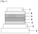
- Figure 1 shows a schematic cross-sectional view of a structure example of the organic EL device used in the present invention.
- the organic EL device of the present invention has one or more light emitting layers between an anode and a cathode opposite to each other, and at least one of the light emitting layers contains a thermally activated delayed fluorescence material (referred to as a TADF material) represented by the general formula (1).
- the organic EL device has a plurality of layers between an anode and a cathode opposite to each other, at least one of the plurality of layers is a light emitting layer, and the light emitting layer may contain a host material, as necessary.
- the organic EL device can contain a light emitting dopant other than the thermally activated delayed fluorescence material represented by the general formula (1).
- X 1 represents O or S.
- X 1 preferably represents S.
- D is independently a nitrogen-containing heterocycle represented by the formula (1a), and the ring Y in the formula (1a) is any of the formulas (1a-1), (1a-2), and (1a-3), preferably the formula (1a-2) or (1a-3), and more preferably the formula (1a-3).
- the ring Y is the formula (1a-1)
- the ring Y is fused at either position d or e.
- the ring Y is the formula (1a-2)
- the ring Y is fused at a position g.
- X 2 represents O, S, or N-Ar 2 , and preferably represents N-Ar 2 .
- the ring Y is fused at any of positions i, j, and k, and preferably fused at a position i.
- a and b each represent the number of substitutions and integer of 0 or 1, provided that a case where a and b are both 0 is excluded.
- Ar 1 to Ar 3 each independently represent a substituted or unsubstituted aromatic hydrocarbon group having 6 to 18 carbon atoms, a substituted or unsubstituted aromatic heterocyclic group having 3 to 17 carbon atoms, or a substituted or unsubstituted linked aromatic group formed by linking 2 to 5 aromatic rings thereof.
- Ar 1 to Ar 3 each represent an unsubstituted aromatic hydrocarbon group having 6 to 15 carbon atoms, a substituted or unsubstituted aromatic heterocyclic group having 3 to 15 carbon atoms, or a substituted or unsubstituted linked aromatic group formed by linking 2 to 4 aromatic rings thereof.
- Ar 1 to Ar 3 each represent an unsubstituted aromatic hydrocarbon group having 6 to 12 carbon atoms, a substituted or unsubstituted aromatic heterocyclic group having 3 to 12 carbon atoms, or a substituted or unsubstituted linked aromatic group formed by linking 2 to 3 aromatic rings thereof.
- the unsubstituted Ar 1 to Ar 3 include a group produced by removing one hydrogen atom from benzene, naphthalene, acenaphthene, acenaphthylene, azulene, anthracene, chrysene, pyrene, phenanthrene, triphenylene, fluorene, benzo[a]anthracene, pyridine, pyrimidine, triazine, thiophene, isothiazole, thiazole, pyridazine, pyrrole, pyrazole, imidazole, triazole, thiadiazole, pyrazine, furan, isoxazole, quinoline, isoquinoline, quinoxaline, quinazoline, thiadiazole, phthalazine, tetrazole, indole, benzofuran, benzothiophene, benzoxazole, benzothiazole, be
- Preferred examples thereof include a group produced by removing one hydrogen atom from benzene, naphthalene, acenaphthene, acenaphthylene, azulene, anthracene, phenanthrene, fluorene, pyridine, pyrimidine, triazine, thiophene, isothiazole, thiazole, pyridazine, pyrrole, pyrazole, imidazole, triazole, thiadiazole, pyrazine, furan, isoxazole, quinoline, isoquinoline, quinoxaline, quinazoline, thiadiazole, phthalazine, tetrazole, indole, benzofuran, benzothiophene, benzoxazole, benzothiazole, indazole, benzimidazole, benzotriazole, benzisothiazole, benzothiadiazole, purine,
- More preferred examples thereof include a group produced by removing one hydrogen atom from benzene, naphthalene, acenaphthene, acenaphthylene, azulene, pyridine, pyrimidine, triazine, thiophene, isothiazole, thiazole, pyridazine, pyrrole, pyrazole, imidazole, triazole, thiadiazole, pyrazine, furan, isoxazole, quinoline, isoquinoline, quinoxaline, quinazoline, thiadiazole, phthalazine, tetrazole, indole, benzofuran, benzothiophene, benzoxazole, benzothiazole, indazole, benzimidazole, benzotriazole, benzisothiazole, benzothiadiazole, purine, pyranone, coumarin, isocoumarin, chromone
- Each of these aromatic hydrocarbon groups, aromatic heterocyclic groups, and linked aromatic groups may have a substituent.
- the substituent is a cyano group, an aliphatic hydrocarbon group having 1 to 10 carbon atoms, a diarylamino group having 12 to 44 carbon atoms, an alkoxy group having 1 to 10 carbon atoms, an aryloxy group having 6 to 18 carbon atoms, an alkylthio group having 1 to 10 carbon atoms, or an arylthio group having 6 to 18 carbon atoms.
- the number of substituents is 0 to 5, and preferably 0 to 2.
- the number of carbon atoms of the substituent is not included in the calculation of the number of carbon atoms. However, it is preferred that the total number of carbon atoms including the number of carbon atoms of the substituent satisfy the above range.
- substituents include cyano, methyl, ethyl, propyl, butyl, pentyl, hexyl, heptyl, octyl, nonyl, decyl, diphenylamino, naphthylphenylamino, dinaphthylamino, dianthranilamino, diphenanthrenylamino, dipyrenylamino, methoxy, ethoxy, phenol, diphenyloxy, methylthio, ethylthio, thiophenol, and diphenylthio.
- Preferred examples thereof include cyano, methyl, ethyl, propyl, butyl, pentyl, hexyl, heptyl, octyl, diphenylamino, naphthylphenylamino, dinaphthylamino, phenol, and thiophenol.
- R 1 to R 4 each independently represent deuterium, an aliphatic hydrocarbon group having 1 to 10 carbon atoms, a substituted or unsubstituted aromatic hydrocarbon group having 6 to 18 carbon atoms, or an aromatic heterocyclic group having 3 to 17 carbon atoms.
- R 1 to R 4 each preferably represent deuterium, an aliphatic hydrocarbon group having 1 to 8 carbon atoms, a substituted or unsubstituted aromatic hydrocarbon group having 6 to 15 carbon atoms, or an aromatic heterocyclic group having 3 to 15 carbon atoms.
- R 1 to R 4 each represent an aliphatic hydrocarbon group having 1 to 6 carbon atoms, a substituted or unsubstituted aromatic hydrocarbon group having 6 to 12 carbon atoms, aromatic heterocyclic group having 3 to 12 carbon atoms, c, f, h, and 1 each represent an integer of 0 to 4.
- R 1 to R 4 are an aliphatic hydrocarbon group having 1 to 10 carbon atoms
- specific examples of R 1 to R 4 include methyl, ethyl, propyl, butyl, pentyl, hexyl, heptyl, octyl, and nonyl.
- Preferred examples thereof include methyl, ethyl, propyl, butyl, pentyl, hexyl, heptyl, and octyl.
- R 1 to R 4 are an unsubstituted aromatic hydrocarbon group having 6 to 18 carbon atoms or an unsubstituted aromatic heterocyclic group having 3 to 17 carbon atoms
- specific examples of R 1 to R 4 include a group produced by removing one hydrogen atom from benzene, naphthalene, acenaphthene, acenaphthylene, azulene, anthracene, chrysene, pyrene, phenanthrene, triphenylene, fluorene, benzo[a]anthracene, pyridine, pyrimidine, triazine, thiophene, isothiazole, thiazole, pyridazine, pyrrole, pyrazole, imidazole, triazole, thiadiazole, pyrazine, furan, isoxazole, quinoline, isoquinoline, quinoxaline, quinazoline, thiadiazole
- Preferred examples thereof include a group produced by removing one hydrogen atom from benzene, naphthalene, acenaphthene, acenaphthylene, azulene, pyridine, pyrimidine, triazine, thiophene, isothiazole, thiazole, pyridazine, pyrrole, pyrazole, imidazole, triazole, thiadiazole, pyrazine, furan, isoxazole, quinoline, isoquinoline, quinoxaline, quinazoline, thiadiazole, phthalazine, tetrazole, indole, benzofuran, benzothiophene, benzoxazole, benzothiazole, indazole, benzimidazole, benzotriazole, benzisothiazole, benzothiadiazole, purine, pyranone, coumarin, isocoumarin, chromone
- More preferred examples thereof include a group produced by removing one hydrogen atom from benzene, naphthalene, azulene, pyridine, pyrimidine, triazine, thiophene, isothiazole, thiazole, pyridazine, pyrrole, pyrazole, imidazole, triazole, thiadiazole, pyrazine, furan, isoxazole, quinoline, isoquinoline, quinoxaline, quinazoline, thiadiazole, phthalazine, tetrazole, indole, benzofuran, benzothiophene, benzoxazole, benzothiazole, indazole, benzimidazole, benzotriazole, benzisothiazole, benzothiadiazole, purine, pyranone, coumarin, isocoumarin, chromone, dibenzofuran, dibenzothiophene, dibenzosele
- Each of these aromatic hydrocarbon groups and aromatic heterocyclic groups may have a substituent.
- the substituent is a cyano group, an aliphatic hydrocarbon group having 1 to 10 carbon atoms, or a diarylamino group having 12 to 44 carbon atoms.
- the number of substituents is 0 to 5, and preferably 0 to 2.
- the number of carbon atoms of the substituent is not included in the calculation of the number of carbon atoms. However, it is preferred that the total number of carbon atoms including the number of carbon atoms of the substituent satisfy the above range.
- substituents include cyano, methyl, ethyl, propyl, butyl, pentyl, hexyl, heptyl, octyl, nonyl, decyl, diphenylamino, naphthylphenylamino, dinaphthylamino, dianthranilamino, and diphenanthrenylamino, dipyrenylamino.
- Preferred examples thereof include cyano, methyl, ethyl, propyl, butyl, pentyl, hexyl, heptyl, octyl, diphenylamino, naphthylphenylamino, and dinaphthylamino.
- thermally activated delayed fluorescence materials represented by the general formula (1) are shown below, but the materials are not limited to these exemplified compounds.
- S1 and T1 are measured as follows.
- a sample compound (thermally activated delayed fluorescence material) is deposited on a quartz substrate by a vacuum deposition method under conditions of a degree of vacuum of 10 -4 Pa or less to form a deposition film having a thickness of 100 nm.
- S1 the emission spectrum of this deposition film is measured, a tangent is drawn to the rise of the emission spectrum on the short-wavelength side, and the wavelength value ⁇ edge [nm] of the point of intersection of the tangent and the horizontal axis is substituted into the following equation (i) to calculate S1.
- S 1 eV 1239.85 / ⁇ edge
- T1 the phosphorescence spectrum of the above deposition film is measured, a tangent is drawn to the rise of the phosphorescence spectrum on the short-wavelength side, and the wavelength value ⁇ edge [nm] of the point of intersection of the tangent and the horizontal axis is substituted into the following equation (ii) to calculate T1.
- T1 eV 1239.85 / ⁇ edge
- thermally activated delayed fluorescence material represented by the general formula (1) as a light emitting dopant or TADF material into a light emitting layer, an excellent delayed fluorescence organic EL device can be provided.
- the light emitting layer can also contain a host material together with the thermally activated delayed fluorescence material represented by the general formula (1), as necessary.
- An excellent organic EL device can be provided by incorporating the host material thereinto.
- the light emitting layer can also contain a fluorescence material other than a compound represented by the general formula (1) as a light emitting dopant together with the thermally activated delayed fluorescence material represented by the general formula (1), as necessary.
- An excellent organic EL device is provided by incorporating a fluorescence material thereinto.
- the light emitting layer can further contain a host material.
- Figure 1 shows a cross-sectional view of a structure example of a typical organic EL device used in the present invention.
- Reference numeral 1 denotes a substrate
- reference numeral 2 denotes an anode
- reference numeral 3 denotes a hole injection layer
- reference numeral 4 denotes a hole transport layer
- reference numeral 5 denotes a light emitting layer
- reference numeral 6 denotes an electron transport layer
- reference numeral 7 denotes a cathode.
- the organic EL device of the present invention may have an exciton blocking layer adjacent to the light emitting layer, or may have an electron blocking layer between the light emitting layer and the hole injection layer.
- the exciton blocking layer may be inserted on either the cathode side or the anode side of the light emitting layer or may be inserted on both sides at the same time.
- the organic EL device of the present invention has the anode, the light emitting layer, and the cathode as essential layers, but preferably has a hole injection/transport layer and an electron injection/transport layer in addition to the essential layers, and further preferably has a hole blocking layer between the light emitting layer and the electron injection/transport layer.
- the hole injection/transport layer means either or both of the hole injection layer and the hole transport layer
- the electron injection/transport layer means either or both of the electron injection layer and electron transport layer.
- the organic EL device of the present invention is preferably supported on a substrate.
- the substrate is not particularly limited and may be a substrate conventionally used for organic EL devices, and for example, a substrate made of glass, transparent plastic, or quartz can be used.
- anode material in the organic EL device a material made of a metal, alloy, or conductive compound having a high work function (4 eV or more), or a mixture thereof is preferably used.
- an electrode material include metals such as Au, and conductive transparent materials such as CuI, indium tin oxide (ITO), SnO 2 , and ZnO.
- An amorphous material capable of producing a transparent conductive film such as IDIXO (In 2 O 3 -ZnO) may also be used.
- these electrode materials may be formed into a thin film by a method such as vapor deposition or sputtering, and then a pattern of a desired form may be formed by photolithography.
- a pattern may be formed through a mask of a desired form at the time of vapor deposition or sputtering of the above electrode materials.
- a coatable material such as an organic conductive compound
- a wet film forming method such as a printing method and a coating method can also be used.
- the transmittance is desirably more than 10%
- the sheet resistance as the anode is preferably several hundred ⁇ /square or less.
- the film thickness is selected within a range of usually 10 to 1,000 nm, and preferably 10 to 200 nm, although it depends on the material.
- a material made of a metal referred to as an electron injection metal), alloy, or conductive compound having a low work function (4 eV or less) or a mixture thereof is used as the cathode material.
- an electrode material include sodium, a sodium-potassium alloy, magnesium, lithium, a magnesium/copper mixture, a magnesium/silver mixture, a magnesium/aluminum mixture, a magnesium/indium mixture, an aluminum/aluminum oxide (Al 2 O 3 ) mixture, indium, a lithium/aluminum mixture, and a rare earth metal.
- a mixture of an electron injection metal with a second metal that has a higher work function value than the electron injection metal and is stable for example, a magnesium/silver mixture, a magnesium/aluminum mixture, a magnesium/indium mixture, an aluminum/aluminum oxide (Al 2 O 3 ) mixture, a lithium/aluminum mixture, or aluminum is suitable.
- the cathode can be produced by forming a thin film from these cathode materials by a method such as vapor deposition and sputtering.
- the sheet resistance as the cathode is preferably several hundred ⁇ /square or less, and the film thickness is selected within a range of usually 10 nm to 5 ⁇ m, and preferably 50 to 200 nm.
- either one of the anode and the cathode of the organic EL device is favorably transparent or translucent because light emission brightness is improved.
- the above metal is formed to have a film thickness of 1 to 20 nm on the cathode, and then a conductive transparent material mentioned in the description of the anode is formed on the metal, so that a transparent or translucent cathode can be produced.
- a device in which both anode and cathode have transmittance can be produced.
- the light emitting layer is a layer that emits light after holes and electrons respectively injected from the anode and the cathode are recombined to form exciton.
- the TADF material represented by the general formula (1) may be used alone, or the TADF material may be used in combination with a host material. When the TADF material is used together with host material, the TADF material serves as a light emitting dopant.
- the TADF material represented by the general formula (1) may also be used together with a fluorescence material other than those represented by the general formula (1).
- the TADF material may be further used together with a host material.
- the fluorescence material serves as a light emitting dopant.
- the content of the light emitting dopant is preferably 0.1 to 50 wt%, and more preferably 1 to 40 wt% based on the host material.
- the host material in the light emitting layer can be a known host material used for a phosphorescent device or a fluorescent device.
- a usable known host material is a compound having the ability to transport hole, the ability to transport electron, and a high glass transition temperature, and preferably has a higher T1 than the T1 of the TADF material represented by the general formula (1).
- a TADF-active compound may also be used as the host material, and the TADF-active compound preferably has ⁇ EST of 0.20 eV or less.
- Known hosts are known in a large number of patent literatures and the like, and hence may be selected from them.
- Specific examples of the host include, but are not particularly limited to, various metal complexes typified by metal complexes of indole derivatives, carbazole derivatives, indolocarbazole derivatives, triazole derivatives, oxazole derivatives, oxadiazole derivatives, imidazole derivatives, phenylenediamine derivatives, arylamine derivatives, styrylanthracene derivatives, fluorenone derivatives, stilbene derivatives, triphenylene derivatives, carborane derivatives, porphyrin derivatives, phthalocyanine derivatives, and 8-quinolinol derivatives, and metal phthalocyanine, and metal complexes of benzoxazole and benzothiazole derivatives; and polymer compounds such as poly(N-vinyl carbazole)derivatives, aniline-based copolymers, thiophen
- each host is deposited from different deposition sources, or a plurality of hosts is premixed before vapor deposition to form a premix, whereby a plurality of hosts can be simultaneously deposited from one deposition source.
- a method by which hosts can be mixed as uniformly as possible is desirable, and examples thereof include, but are not limited to, milling, a method of heating and melting hosts under reduced pressure or under an inert gas atmosphere such as nitrogen, and sublimation.
- the host and a premix thereof may be in the form of powder, sticks, or granules.
- Preferred examples of the host specifically include, but are not particularly limited to, the following.
- fluorescence material other than those represented by the general formula (1) when a fluorescence material other than those represented by the general formula (1) is used in the light emitting layer, preferred examples of the other fluorescence material include fused polycyclic aromatic derivatives, styrylamine derivatives, fused ring amine derivatives, boron-containing compounds, pyrrole derivatives, indole derivatives, carbazole derivatives, and indolocarbazole derivatives. Among them, fused ring amine derivatives, boron-containing compounds, carbazole derivatives, and indolocarbazole derivatives are preferred.
- fused ring amine derivatives examples include diaminepyrene derivatives, diaminochrysene derivatives, diaminoanthracene derivatives, diaminofluorenone derivatives, and diaminofluorene derivatives fused with one or more benzofuro backbones.
- Examples of the boron-containing compounds include pyrromethene derivatives and trriphenylborane derivatives.
- Preferred examples of the fluorescence material other than those represented by the general formula (1) are not particularly limited, but specific examples thereof include the following.
- the injection layer refers to a layer provided between the electrode and the organic layer to reduce the driving voltage and improve the light emission brightness, and includes the hole injection layer and the electron injection layer.
- the injection layer may be present between the anode and the light emitting layer or the hole transport layer, as well as between the cathode and the light emitting layer or the electron transport layer.
- the injection layer may be provided as necessary.
- the hole blocking layer has the function of the electron transport layer in a broad sense, is made of a hole blocking material having a very small ability to transport holes while having the function of transporting electrons, and can improve the recombination probability between the electrons and the holes in the light emitting layer by blocking the holes while transporting the electrons.
- a known hole blocking material can be used for the hole blocking layer.
- a plurality of hole blocking materials may be used in combination.
- the electron blocking layer has the function of the hole transport layer in a broad sense, and can improve the recombination probability between the electrons and the holes in the light emitting layer by blocking the electrons while transporting the holes.
- a known material for the electron blocking layer can be used as the material for the electron blocking layer.
- the exciton blocking layer is a layer to block the diffusion of the excitons generated by recombination of the holes and the electrons in the light emitting layer into a charge transport layer, and insertion of this layer makes it possible to efficiently keep the excitons in the light emitting layer, so that the emission efficiency of the device can be improved.
- the exciton blocking layer can be inserted between two light emitting layers adjacent to each other in the device in which two or more light emitting layers are adjacent to each other.
- a known material for the exciton blocking layer can be used as the material for such an exciton blocking layer.
- the layer adjacent to the light emitting layer includes the hole blocking layer, the electron blocking layer, and the exciton blocking layer, and when these layers are not provided, the adjacent layer is the hole transport layer, the electron transport layer, and the like.
- the hole transport layer is made of a hole transport material having the function of transporting holes, and the hole transport layer may be provided as a single layer or a plurality of layers.
- the hole transport material has any of hole injection properties, hole transport properties, or electron barrier properties, and may be either an organic material or an inorganic material.
- the hole transport layer any of conventionally known compounds may be selected and used.
- Examples of such a hole transport material include porphyrin derivatives, arylamine derivatives, triazole derivatives, oxadiazole derivatives, imidazole derivatives, polyarylalkane derivatives, phenylenediamine derivatives, arylamine derivatives, amino-substituted chalcone derivatives, oxazole derivatives, styrylanthracene derivatives, fluorenone derivatives, hydrazone derivatives, stilbene derivatives, silazane derivatives, aniline-based copolymers, and conductive polymer oligomers, particularly, thiophene oligomers.
- Porphyrin derivatives, arylamine derivatives, and styrylamine derivatives are preferably used, and arylamine compounds are
- the electron transport layer is made of a material having the function of transporting electrons, and the electron transport layer may be provided as a single layer or a plurality of layers.
- the electron transport material (may also serve as the hole blocking material) has the function of transmitting electrons injected from the cathode to the light emitting layer.
- any of conventionally known compounds may be selected and used, and examples thereof include polycyclic aromatic derivatives such as naphthalene, anthracene, and phenanthroline, tris(8-quinolinolato)aluminum (III) derivatives, phosphine oxide derivatives, nitro-substituted fluorene derivatives, diphenylquinone derivatives, thiopyran dioxide derivatives, carbodiimides, fluorenylidene methane derivatives, anthraquinodimethane and anthrone derivatives, bipyridine derivatives, quinoline derivatives, oxadiazole derivatives, benzimidazole derivatives, benzothiazole derivatives, and indolocarbazole derivatives. Further, polymer materials in which these materials are introduced in the polymer chain or these
- the film formation method of each layer is not particularly limited, and the layers may be produced by either a dry process or a wet process.
- the fluorescence lifetime of the compound 1-15 obtained in Synthesis Example 1 was measured as follows.
- the compound 1-15 and BH-1 shown hereinabove were deposited on a quartz substrate from different deposition sources by a vacuum deposition method under conditions of a degree of vacuum of 10 -4 Pa or less to form a co-deposition film having a thickness of 100 nm such that the concentration of the compound 1-15 was 30% by mass.
- the emission spectrum of this thin film was measured, it was confirmed that the emission peaked at 473 nm.
- the emission lifetime was also measured by a compact fluorescence lifetime measuring apparatus (Quantaurus-tau, manufactured by Hamamatsu Photonics K.K.) under a nitrogen atmosphere.
- the fluorescence emission with an emission lifetime of 1.6 ns and the delayed fluorescence emission with an emission lifetime of 1.9 ⁇ s were observed, which confirmed that the compound 1-15 is a compound showing delayed fluorescence emission.
- the fluorescence lifetime of the compound 1-11 obtained in Synthesis Example 2 was measured as follows.
- the compound 1-11 and BH-1 shown hereinabove were deposited on a quartz substrate from different deposition sources by a vacuum deposition method under conditions of a degree of vacuum of 10 -4 Pa or less to form a co-deposition film having a thickness of 100 nm such that the concentration of the compound 1-11 was 30% by mass.
- the emission spectrum of this thin film was measured, it was confirmed that the emission peaked at 473 nm.
- the emission lifetime was also measured by a compact fluorescence lifetime measuring apparatus (Quantaurus-tau, manufactured by Hamamatsu Photonics K.K.) under a nitrogen atmosphere.
- the fluorescence emission with an emission lifetime of 2.0 ns and the delayed fluorescence emission with an emission lifetime of 1.7 ⁇ s were observed, which confirmed that the compound 1-11 is a compound showing delayed fluorescence emission.
- the fluorescence lifetime of the compound 1-81 obtained in Synthesis Example 3 was measured as follows.
- the compound 1-81 and BH-1 shown hereinabove were deposited on a quartz substrate from different deposition sources by a vacuum deposition method under conditions of a degree of vacuum of 10 -4 Pa or less to form a co-deposition film having a thickness of 100 nm such that the concentration of the compound 1-81 was 30% by mass.
- the emission spectrum of this thin film was measured, it was confirmed that the emission peaked at 455 nm.
- the emission lifetime was also measured by a compact fluorescence lifetime measuring apparatus (Quantaurus-tau, manufactured by Hamamatsu Photonics K.K.) under a nitrogen atmosphere.
- the fluorescence emission with an emission lifetime of 7.4 ns and the delayed fluorescence emission with an emission lifetime of 1.5 ⁇ s were observed, which confirmed that the compound 1-81 is a compound showing delayed fluorescence emission.
- TD-1 and the previously presented BH-1 were deposited on a quartz substrate from different deposition sources by a vacuum deposition method under conditions of a degree of vacuum of 10 -4 Pa or less to form a co-deposition film having a thickness of 100 nm such that the concentration of the TD-1 was 30% by mass.
- the emission spectrum of this thin film was measured, it was confirmed that the emission peaked at 454 nm.
- the emission lifetime was also measured by a compact fluorescence lifetime measuring apparatus (Quantaurus-tau, manufactured by Hamamatsu Photonics K.K.) under a nitrogen atmosphere.
- the fluorescence emission with an emission lifetime of 12.7 ns and the delayed fluorescence emission with an emission lifetime of 1.0 ⁇ s were observed, which confirmed that the TD-1 is a compound showing delayed fluorescence emission.
- Each thin film shown below was laminated on the glass substrate on which an anode made of ITO having a film thickness of 70 nm was formed by a vacuum deposition method at a degree of vacuum of 4.0 ⁇ 10 -5 Pa.
- the previously presented HAT-CN was formed on ITO to a thickness of 10 nm as a hole injection layer, and then HT-1 was formed to a thickness of 25 nm as a hole transport layer.
- BH-1 was formed to a thickness of 5 nm as an electron blocking layer.
- BH-1 as the host and a compound (1-15) as the dopant were co-deposited from different deposition sources to form a light emitting layer having a thickness of 30 nm.
- HBL-1 was formed to a thickness of 5 nm as a hole blocking layer.
- ET-1 was formed to a thickness of 40 nm as an electron transport layer.
- lithium fluoride (LiF) was formed on the electron transport layer to a thickness of 1 nm as an electron injection layer.
- Al aluminum
- Each organic EL device was produced in the same manner as in Example 1, except that the dopant was changed to the compound (1-11).
- Each organic EL device was produced in the same manner as in Example 1, except that the dopant was changed to the compounds (1-81).
- Each thin film shown below was laminated on the glass substrate on which an anode made of ITO having a film thickness of 70 nm was formed, by a vacuum deposition method at a degree of vacuum of 4.0 ⁇ 10 -5 Pa.
- the previously presented HAT-CN was formed on ITO to a thickness of 10 nm as a hole injection layer, and then HT-1 was formed to a thickness of 25 nm as a hole transport layer.
- BH-1 was formed to a thickness of 5 nm as an electron blocking layer.
- BH-1 as the host, the compound (1-11) as the TADF material, and BD-1 as the dopant were co-deposited from different deposition sources to form a light emitting layer having a thickness of 30 nm.
- HBL-1 was formed to a thickness of 5 nm as a hole blocking layer.
- ET-1 was formed to a thickness of 40 nm as an electron transport layer.
- lithium fluoride (LiF) was formed on the electron transport layer to a thickness of 1 nm as an electron injection layer.
- Al aluminum
- Each organic EL device was produced in the same manner as in Example 1, except that the dopant was changed to the TD-1.
- the maximum emission wavelength of the emission spectrum, external quantum efficiency, and lifetime of each organic EL device produced are shown in Table 2.
- the maximum emission wavelength and the external quantum efficiency were values at a driving current density of 2.5 mA/cm 2 and were initial characteristics.
- the time taken for the luminance to reduce to 50% of the initial luminance when the initial luminance was 500 cd/m 2 was measured as the lifetime.
- the organic EL device including, as a light emitting dopant, the TADF material represented by the general formula (1), in which a boron-containing electron acceptor backbone is linked with an electron donor backbone having a specific fused ring structure, showed excellent results in both efficiency and lifetime as can be seen from the comparison with Comparative Example 1. It is considered that the reason for this is as follows: the use of an electron donor backbone having a specific fused ring structure reduced ⁇ EST and facilitated the development of TADF characteristics to thereby improve the efficiency; and in addition, the use of an electron donor backbone having a specific fused ring structure improved the stability against oxidation and the lifetime characteristics.
Landscapes
- Chemical & Material Sciences (AREA)
- Engineering & Computer Science (AREA)
- Materials Engineering (AREA)
- Organic Chemistry (AREA)
- Physics & Mathematics (AREA)
- Spectroscopy & Molecular Physics (AREA)
- Crystallography & Structural Chemistry (AREA)
- Inorganic Chemistry (AREA)
- Nanotechnology (AREA)
- Optics & Photonics (AREA)
- Electroluminescent Light Sources (AREA)
Applications Claiming Priority (2)
| Application Number | Priority Date | Filing Date | Title |
|---|---|---|---|
| JP2020118001 | 2020-07-08 | ||
| PCT/JP2021/025469 WO2022009883A1 (ja) | 2020-07-08 | 2021-07-06 | 熱活性化遅延蛍光材料、及び有機電界発光素子 |
Publications (1)
| Publication Number | Publication Date |
|---|---|
| EP4180500A1 true EP4180500A1 (de) | 2023-05-17 |
Family
ID=79553141
Family Applications (1)
| Application Number | Title | Priority Date | Filing Date |
|---|---|---|---|
| EP21837328.0A Withdrawn EP4180500A1 (de) | 2020-07-08 | 2021-07-06 | Wärmeaktiviertes verzögertes fluoreszenzmaterial und organisches elektrolumineszenzelement |
Country Status (6)
| Country | Link |
|---|---|
| US (1) | US20230309400A1 (de) |
| EP (1) | EP4180500A1 (de) |
| JP (1) | JPWO2022009883A1 (de) |
| KR (1) | KR20230035528A (de) |
| CN (1) | CN115943193A (de) |
| WO (1) | WO2022009883A1 (de) |
Family Cites Families (6)
| Publication number | Priority date | Publication date | Assignee | Title |
|---|---|---|---|---|
| US20100295444A1 (en) | 2009-05-22 | 2010-11-25 | Idemitsu Kosan Co., Ltd. | Organic electroluminescence device |
| EP3176241A1 (de) | 2009-12-07 | 2017-06-07 | Nippon Steel & Sumikin Chemical Co., Ltd. | Organisches lichtemittierendes material und organisches lichtemittierendes element |
| TWI599570B (zh) | 2012-09-28 | 2017-09-21 | 新日鐵住金化學股份有限公司 | Compounds for organic electroluminescent devices and organic electroluminescent devices |
| WO2015072537A1 (ja) | 2013-11-18 | 2015-05-21 | 国立大学法人九州大学 | 発光材料、有機発光素子および化合物 |
| US20180366653A1 (en) * | 2015-12-04 | 2018-12-20 | Guangzhou Chinaray Optoelectronic Materials Ltd. | D-a type compound and application thereof |
| CN110698504B (zh) * | 2019-10-31 | 2022-02-25 | 武汉天马微电子有限公司 | 硼杂环化合物、显示面板以及显示装置 |
-
2021
- 2021-07-06 CN CN202180044870.7A patent/CN115943193A/zh active Pending
- 2021-07-06 KR KR1020227044920A patent/KR20230035528A/ko unknown
- 2021-07-06 WO PCT/JP2021/025469 patent/WO2022009883A1/ja active Search and Examination
- 2021-07-06 EP EP21837328.0A patent/EP4180500A1/de not_active Withdrawn
- 2021-07-06 JP JP2022535348A patent/JPWO2022009883A1/ja active Pending
- 2021-07-06 US US18/011,403 patent/US20230309400A1/en active Pending
Also Published As
| Publication number | Publication date |
|---|---|
| US20230309400A1 (en) | 2023-09-28 |
| CN115943193A (zh) | 2023-04-07 |
| KR20230035528A (ko) | 2023-03-14 |
| WO2022009883A1 (ja) | 2022-01-13 |
| JPWO2022009883A1 (de) | 2022-01-13 |
Similar Documents
| Publication | Publication Date | Title |
|---|---|---|
| WO2018173598A1 (ja) | 有機電界発光素子 | |
| EP3399566B1 (de) | Organisches elektrolumineszenzelement | |
| EP4130191A1 (de) | Organische elektrolumineszente vorrichtung | |
| CN113614202A (zh) | 有机电场发光元件用熔融混合物、及有机电场发光元件 | |
| EP4276925A1 (de) | Organisches elektrolumineszenzelement und verfahren zu seiner herstellung | |
| KR102691086B1 (ko) | 유기 전계 발광 소자 | |
| EP4083033A1 (de) | Organisches elektrolumineszentes element | |
| EP3767698B1 (de) | Organisches elektrolumineszentes element | |
| WO2022254965A1 (ja) | 化合物、発光材料および発光素子 | |
| EP4130194A1 (de) | Organisches elektrolumineszenzelement | |
| EP4180500A1 (de) | Wärmeaktiviertes verzögertes fluoreszenzmaterial und organisches elektrolumineszenzelement | |
| EP3399565A1 (de) | Organisches elektrolumineszenzelement | |
| EP4234562A1 (de) | Lichtemittierendes material und organisches elektrolumineszenzelement | |
| EP4322236A1 (de) | Lichtemittierendes material und organisches elektrolumineszenzelement | |
| JP2020105341A (ja) | 熱活性化遅延蛍光発光材料、及び有機電界発光素子 | |
| US20240224800A1 (en) | Material for organic electroluminescent elements, and organic electroluminescent element | |
| EP4234556A1 (de) | Material für ein organisches elektrolumineszenzelement und organisches elektrolumineszenzelement | |
| EP4206301A1 (de) | Organisches elektrolumineszenzelement | |
| WO2024058146A1 (ja) | 発光材料、及び有機電界発光素子 | |
| EP4130192A1 (de) | Organische elektrolumineszente vorrichtung | |
| WO2023157629A1 (ja) | 発光材料、及び有機電界発光素子 | |
| EP4261910A1 (de) | Material für ein organisches elektrolumineszenzelement und organisches elektrolumineszenzelement | |
| WO2024019072A1 (ja) | 有機電界発光素子 | |
| CN118614162A (zh) | 有机电场发光元件用材料、及有机电场发光元件 | |
| CN115443551A (zh) | 有机电场发光元件用材料及有机电场发光元件 |
Legal Events
| Date | Code | Title | Description |
|---|---|---|---|
| STAA | Information on the status of an ep patent application or granted ep patent |
Free format text: STATUS: THE INTERNATIONAL PUBLICATION HAS BEEN MADE |
|
| PUAI | Public reference made under article 153(3) epc to a published international application that has entered the european phase |
Free format text: ORIGINAL CODE: 0009012 |
|
| STAA | Information on the status of an ep patent application or granted ep patent |
Free format text: STATUS: REQUEST FOR EXAMINATION WAS MADE |
|
| 17P | Request for examination filed |
Effective date: 20230129 |
|
| AK | Designated contracting states |
Kind code of ref document: A1 Designated state(s): AL AT BE BG CH CY CZ DE DK EE ES FI FR GB GR HR HU IE IS IT LI LT LU LV MC MK MT NL NO PL PT RO RS SE SI SK SM TR |
|
| DAV | Request for validation of the european patent (deleted) | ||
| DAX | Request for extension of the european patent (deleted) | ||
| STAA | Information on the status of an ep patent application or granted ep patent |
Free format text: STATUS: THE APPLICATION HAS BEEN WITHDRAWN |
|
| 18W | Application withdrawn |
Effective date: 20240612 |