EP2882002A1 - Unité de source lumineuse - Google Patents
Unité de source lumineuse Download PDFInfo
- Publication number
- EP2882002A1 EP2882002A1 EP13826194.6A EP13826194A EP2882002A1 EP 2882002 A1 EP2882002 A1 EP 2882002A1 EP 13826194 A EP13826194 A EP 13826194A EP 2882002 A1 EP2882002 A1 EP 2882002A1
- Authority
- EP
- European Patent Office
- Prior art keywords
- strip
- wiring
- led elements
- wirings
- light source
- Prior art date
- Legal status (The legal status is an assumption and is not a legal conclusion. Google has not performed a legal analysis and makes no representation as to the accuracy of the status listed.)
- Granted
Links
Images


Classifications
-
- F—MECHANICAL ENGINEERING; LIGHTING; HEATING; WEAPONS; BLASTING
- F21—LIGHTING
- F21V—FUNCTIONAL FEATURES OR DETAILS OF LIGHTING DEVICES OR SYSTEMS THEREOF; STRUCTURAL COMBINATIONS OF LIGHTING DEVICES WITH OTHER ARTICLES, NOT OTHERWISE PROVIDED FOR
- F21V23/00—Arrangement of electric circuit elements in or on lighting devices
- F21V23/003—Arrangement of electric circuit elements in or on lighting devices the elements being electronics drivers or controllers for operating the light source, e.g. for a LED array
- F21V23/004—Arrangement of electric circuit elements in or on lighting devices the elements being electronics drivers or controllers for operating the light source, e.g. for a LED array arranged on a substrate, e.g. a printed circuit board
- F21V23/005—Arrangement of electric circuit elements in or on lighting devices the elements being electronics drivers or controllers for operating the light source, e.g. for a LED array arranged on a substrate, e.g. a printed circuit board the substrate is supporting also the light source
-
- F—MECHANICAL ENGINEERING; LIGHTING; HEATING; WEAPONS; BLASTING
- F21—LIGHTING
- F21V—FUNCTIONAL FEATURES OR DETAILS OF LIGHTING DEVICES OR SYSTEMS THEREOF; STRUCTURAL COMBINATIONS OF LIGHTING DEVICES WITH OTHER ARTICLES, NOT OTHERWISE PROVIDED FOR
- F21V23/00—Arrangement of electric circuit elements in or on lighting devices
- F21V23/06—Arrangement of electric circuit elements in or on lighting devices the elements being coupling devices, e.g. connectors
-
- F—MECHANICAL ENGINEERING; LIGHTING; HEATING; WEAPONS; BLASTING
- F21—LIGHTING
- F21V—FUNCTIONAL FEATURES OR DETAILS OF LIGHTING DEVICES OR SYSTEMS THEREOF; STRUCTURAL COMBINATIONS OF LIGHTING DEVICES WITH OTHER ARTICLES, NOT OTHERWISE PROVIDED FOR
- F21V29/00—Protecting lighting devices from thermal damage; Cooling or heating arrangements specially adapted for lighting devices or systems
- F21V29/50—Cooling arrangements
- F21V29/70—Cooling arrangements characterised by passive heat-dissipating elements, e.g. heat-sinks
-
- H—ELECTRICITY
- H10—SEMICONDUCTOR DEVICES; ELECTRIC SOLID-STATE DEVICES NOT OTHERWISE PROVIDED FOR
- H10H—INORGANIC LIGHT-EMITTING SEMICONDUCTOR DEVICES HAVING POTENTIAL BARRIERS
- H10H20/00—Individual inorganic light-emitting semiconductor devices having potential barriers, e.g. light-emitting diodes [LED]
- H10H20/80—Constructional details
- H10H20/81—Bodies
- H10H20/813—Bodies having a plurality of light-emitting regions, e.g. multi-junction LEDs or light-emitting devices having photoluminescent regions within the bodies
-
- H—ELECTRICITY
- H10—SEMICONDUCTOR DEVICES; ELECTRIC SOLID-STATE DEVICES NOT OTHERWISE PROVIDED FOR
- H10H—INORGANIC LIGHT-EMITTING SEMICONDUCTOR DEVICES HAVING POTENTIAL BARRIERS
- H10H20/00—Individual inorganic light-emitting semiconductor devices having potential barriers, e.g. light-emitting diodes [LED]
- H10H20/80—Constructional details
- H10H20/85—Packages
- H10H20/857—Interconnections, e.g. lead-frames, bond wires or solder balls
-
- H—ELECTRICITY
- H10—SEMICONDUCTOR DEVICES; ELECTRIC SOLID-STATE DEVICES NOT OTHERWISE PROVIDED FOR
- H10W—GENERIC PACKAGES, INTERCONNECTIONS, CONNECTORS OR OTHER CONSTRUCTIONAL DETAILS OF DEVICES COVERED BY CLASS H10
- H10W72/00—Interconnections or connectors in packages
- H10W72/30—Die-attach connectors
-
- H—ELECTRICITY
- H10—SEMICONDUCTOR DEVICES; ELECTRIC SOLID-STATE DEVICES NOT OTHERWISE PROVIDED FOR
- H10W—GENERIC PACKAGES, INTERCONNECTIONS, CONNECTORS OR OTHER CONSTRUCTIONAL DETAILS OF DEVICES COVERED BY CLASS H10
- H10W90/00—Package configurations
-
- F—MECHANICAL ENGINEERING; LIGHTING; HEATING; WEAPONS; BLASTING
- F21—LIGHTING
- F21Y—INDEXING SCHEME ASSOCIATED WITH SUBCLASSES F21K, F21L, F21S and F21V, RELATING TO THE FORM OR THE KIND OF THE LIGHT SOURCES OR OF THE COLOUR OF THE LIGHT EMITTED
- F21Y2105/00—Planar light sources
- F21Y2105/10—Planar light sources comprising a two-dimensional [2D] array of point-like light-generating elements
-
- F—MECHANICAL ENGINEERING; LIGHTING; HEATING; WEAPONS; BLASTING
- F21—LIGHTING
- F21Y—INDEXING SCHEME ASSOCIATED WITH SUBCLASSES F21K, F21L, F21S and F21V, RELATING TO THE FORM OR THE KIND OF THE LIGHT SOURCES OR OF THE COLOUR OF THE LIGHT EMITTED
- F21Y2115/00—Light-generating elements of semiconductor light sources
- F21Y2115/10—Light-emitting diodes [LED]
-
- H—ELECTRICITY
- H10—SEMICONDUCTOR DEVICES; ELECTRIC SOLID-STATE DEVICES NOT OTHERWISE PROVIDED FOR
- H10W—GENERIC PACKAGES, INTERCONNECTIONS, CONNECTORS OR OTHER CONSTRUCTIONAL DETAILS OF DEVICES COVERED BY CLASS H10
- H10W72/00—Interconnections or connectors in packages
- H10W72/01—Manufacture or treatment
- H10W72/013—Manufacture or treatment of die-attach connectors
- H10W72/01308—Manufacture or treatment of die-attach connectors using permanent auxiliary members, e.g. using alignment marks
-
- H—ELECTRICITY
- H10—SEMICONDUCTOR DEVICES; ELECTRIC SOLID-STATE DEVICES NOT OTHERWISE PROVIDED FOR
- H10W—GENERIC PACKAGES, INTERCONNECTIONS, CONNECTORS OR OTHER CONSTRUCTIONAL DETAILS OF DEVICES COVERED BY CLASS H10
- H10W72/00—Interconnections or connectors in packages
- H10W72/30—Die-attach connectors
- H10W72/381—Auxiliary members
- H10W72/387—Flow barriers
-
- H—ELECTRICITY
- H10—SEMICONDUCTOR DEVICES; ELECTRIC SOLID-STATE DEVICES NOT OTHERWISE PROVIDED FOR
- H10W—GENERIC PACKAGES, INTERCONNECTIONS, CONNECTORS OR OTHER CONSTRUCTIONAL DETAILS OF DEVICES COVERED BY CLASS H10
- H10W72/00—Interconnections or connectors in packages
- H10W72/851—Dispositions of multiple connectors or interconnections
- H10W72/874—On different surfaces
- H10W72/884—Die-attach connectors and bond wires
-
- H—ELECTRICITY
- H10—SEMICONDUCTOR DEVICES; ELECTRIC SOLID-STATE DEVICES NOT OTHERWISE PROVIDED FOR
- H10W—GENERIC PACKAGES, INTERCONNECTIONS, CONNECTORS OR OTHER CONSTRUCTIONAL DETAILS OF DEVICES COVERED BY CLASS H10
- H10W90/00—Package configurations
- H10W90/701—Package configurations characterised by the relative positions of pads or connectors relative to package parts
- H10W90/731—Package configurations characterised by the relative positions of pads or connectors relative to package parts of die-attach connectors
- H10W90/734—Package configurations characterised by the relative positions of pads or connectors relative to package parts of die-attach connectors between a chip and a stacked insulating package substrate, interposer or RDL
Definitions
- the present invention relates to a light source unit, and more particularly a light source unit that has a substrate and a plurality of LED elements on the substrate.
- a light source that can emit ultraviolet light is often used as a light source to cure, dry, melt, soften or reform an object to be treated (e.g., a protection film, an adhesive, painting, an ink, a photoresist, resin, and oriented film).
- an LED element is becoming popular as the light source that emits light in an ultraviolet range (UV range).
- UV range ultraviolet range
- An ultraviolet light source unit that uses the LED element(s) to emit light in the UV range is therefore studied.
- Patent Literature 1 One example of a configuration that includes the light source unit having the LED element(s) together with an ink jet head of an ink jet printer is disclosed in Japanese Patent Application Laid-Open Publication No. 2004-358769 (Patent Literature 1; will be mentioned below).
- An ink jet printer 20 includes an ink jet head 21 to inject an ink to a print medium M such as paper, and ultraviolet light source units 22 located on one side (or both sides) of the ink jet head 21.
- the ink jet head 21 and the ultraviolet light source units 22 are situated above the print medium M by a predetermined distance, and supported from a guide rail 23 such that the ink jet head and the ultraviolet light source units can move (scan) in a transverse direction X relative to the print medium M.
- a UV ink droplet injected from the ink jet head 21 and adhering to the surface of the print medium M is cured by the ultraviolet light emitted from the light source unit(s) 22. Accordingly, the UV ink is successively cured (fixed) on the surface of the print medium M in the scanning direction X of the ink jet head 21.
- the print medium M is moved a prescribed distance in the length direction Y, and the above-mentioned printing is repeated. In this manner, a picture (drawing, painting) or a character (letter) is made on the surface of the print medium M.
- the ultraviolet light source unit provided in the ink jet printer has LED elements that are arranged zigzag (staggered).
- Fig. 16 of the accompanying drawings shows the arrangement of the LED elements.
- a light irradiation surface of the ultraviolet light source unit 22 has a substrate 222, on which the LED elements 221 are disposed.
- the LED elements 221 are situated on the substrate 222 zigzag in the longitudinal direction and the transverse direction. With such zigzag arrangement of the LED elements, the ultraviolet light source unit 22 can emit the ultraviolet light uniformly, without gaps, along the traveling path of the ultraviolet light source unit 22 when the ultraviolet light source unit 22 is moved.
- the light source unit is brought into the unlit condition.
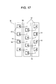
- Fig. 17 a different wiring arrangement as shown in Fig. 17 .
- a plurality of parallel linear or narrow strip-like wirings 12 are arranged in the same direction on the substrate 11.
- a plurality of LED elements 13 are connected to each of the strip-like wirings 12 by soldering.
- the LED elements 13 are arranged zigzag.
- Each of the LED elements 13 on each strip-like wiring 12 has an upper face electrode 14, and a wire 15 extending from the upper face electrode 14 is electrically connected to a region 16 of a next strip-like wiring 12 between each two adjacent LED elements 13 on that strip-like wiring 12 by wire bonding.
- each strip-like wiring 12 becomes a common electrode for the LED elements 13 disposed on that strip-like wiring 12.
- the LED elements 13 on each strip-like wiring 12 are electrically connected in parallel to each other.
- Such wiring configuration brings about an advantage that even when one of the wires 15 of the LED elements 13 is disconnected, other LED elements are not unlit correspondingly.
- the LED elements 13 are joined to the strip-like wirings 12 by soldering, and the LED elements 13 on one strip-like wiring are connected to the neighboring strip-like wiring 12 at the regions 16 between the LED elements 13 on that strip-like wiring 12 by the wires 15.
- the LED elements 13 on one strip-like wiring are soldered to the strip-like wiring 12 on the neighboring strip-like wiring, the solder 17 and fluxes contained in the solder 17 are melted, and flow from the lower faces of the LED elements 13. It is difficult to control (regulate) the outflow of the solder 17.
- the LED elements 13 are arranged at intervals as small as possible from the viewpoint of reducing the installation areas of the LED elements 13. Thus, the solder 17 that is used to connect one LED element 13 often becomes continuous to the spilled solder from an adjacent LED element 13.
- the ink jet and the light source unit need to move quickly in the transverse direction X.
- an amount of ultraviolet light irradiation that is directed to the UV ink droplet injected from the ink jet head per unit time becomes smaller. Accordingly, the ink is not cured sufficiently.
- the inventors studied the possible high density arrangement of the LED elements and the strip-like wirings on the substrate, i.e., the inventors studied the above-described configuration as shown in Fig. 17 .
- the LED element 13 has the electrode 14 on its upper face and the electrode 18 on its lower face.
- the electrode 18 attached to the lower face is connected to the strip-like wiring 12 by soldering or the like.
- the electrode 14 attached to the upper face is connected to the adjacent strip-like wiring 12 between the LED elements 13 by the wire 15.
- the strip-like wirings 12 should be insulated from each other such that the electric circuits formed by the respective strip-like wirings 12 are insulated from each other. Thus, the strip-like wirings 12 are spaced from each other at prescribed intervals for insulation (gaps for insulation).
- the heat sink HS is provided in contact with the lower face of the substrate 11. Heat of the substrate is radiated from the heat sink HS with the cooling air from a cooling fan. Thus, the substrate 11 is cooled. With such configuration, the heat generated from the LED elements 13 is radiated through the lower face electrode 18, the strip-like wiring 12, the substrate 11 and the heat sink HS in this order (heat radiation route from the LED lower face electrode to the heat sink).
- the strip-like wirings 12 should have the prescribed insulation gaps (should be spaced from each other). In the end, this becomes an obstacle, i.e., this makes it difficult to arrange the LED elements 13 on the strip-like wirings 12 at a high density in the X-direction perpendicular to the longitudinal direction of the strip-like wirings 12.
- each strip-like wiring 12 may be made smaller than the width of the LED element 13.
- Such strip-like wirings 12 may be arranged in parallel, and the LED elements 13 may be disposed on the strip-like wirings 12 to increase the arrangement density (installation density) of the LED elements 13 in the X-direction.
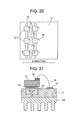
- Fig. 20 illustrates the above-described structure.
- each of the strip-like wirings 12 on the substrate 11 has a smaller width than each LED element 13.
- a plurality of LED elements 13 are arranged on each wiring 12.
- each of the strip-like wirings 12 Because the width of each of the strip-like wirings 12 is reduced, the insulation gap between each two adjacent wirings 12 is reduced, as compared to the configuration shown in Fig. 17 , even if the wirings 12 are spaced from each other at the prescribed insulation gaps. Accordingly, the LED elements 13 disposed on the wirings 12 may be arranged at a higher density in the X-direction, which is perpendicular to the longitudinal direction of the wirings 12.
- the width L1 of the strip-like wiring 12 on the substrate 11 becomes smaller than the width of the LED element 13, as shown in Fig. 21 which is the cross-sectional view taken along the line A-A in Fig. 20 . If the installation density should be further reduced in the X-direction of Fig. 20 , then the width L1 would become smaller than the width L2 of the lower face electrode 18 of the LED element 13 (L1 ⁇ L2). This makes the heat radiation route from the LED element 13 to the heat sink HS narrow(er) at the strip-like wiring 12, and deteriorates the heat radiation capability. As a result, a sufficient cooling effect is not given to the LED elements, and the luminous efficacy (light emission efficiency) of the LED elements drops.
- PATENT LITERATURE 1 Japanese Patent Application Laid-Open Publication No. 2004-358769
- the present invention intends to provide a light source unit that includes a substrate, a plurality of parallel strip-like wirings on the substrate, and a plurality of LED elements on the strip-like wirings, and that does not suffer from the poor connection.
- the LED elements soldered onto one strip-like wiring are electrically connected to an adjacent strip-like wiring by wires.
- the LED elements are arranged, as a whole, on the substrate in a staggered manner.
- the wires extending from the LED elements on one strip-like wiring are reliably connected to an adjacent strip-like wiring, and therefore poor connection does not occur.
- the present invention intends to provide a configuration that can increase the installation density of the LED elements on the substrate, and can ensure the sufficient cooling to the LED elements to prevent the drop of the luminous efficacy.
- the light source unit includes one or more damming grooves (intercepting grooves, halting grooves) between each two adjacent LED elements on each strip-like wiring.
- the damming groove(s) form(s) a non-effusion region (no-solder-effusing region) between each two adjacent LED elements.
- the non-effusion region is a region into which no solder flows.
- the wires are electrically connected to the non-effusion regions.
- Two damming grooves may be formed between each two adjacent LED elements on each strip-like wiring.
- the two damming grooves may extend transversely across the strip-like wiring concerned, and form the non-effusion region between the two damming grooves.
- Each damming groove may include a series of dot-like concaves that extend transversely across the strip-like wiring concerned.
- Each of the damming grooves may be an annular groove formed between each two adjacent LED elements on each strip-like wiring, and the annular groove may form the non-effusion region therein.
- Each of the damming grooves may be an annular groove that surrounds each LED element, and the annular groove may form the non-effusion region outside the annular groove.
- Two L-shaped damming grooves may be formed in the vicinity of diagonally opposite corners of each LED element.
- the L-shaped grooves may be formed outside the associated LED element.
- the non-effusion region may be formed outside the L-shaped grooves.
- each strip-like wiring of the light source unit has wide parts (large parts) and narrow parts (small parts) in a wiring direction (longitudinal direction of the strip-like wiring).
- the LED elements are disposed on the wide parts of the strip-like wirings.
- the LED elements are disposed on the wide parts of the strip-like wirings.
- Damming grooves may be formed in each strip-like wiring such that at least one damming groove is provided between each two adjacent LED elements on each strip-like wiring.
- Non-effusion regions, into which no solder flows, may be formed on the narrow parts.
- Each of the wide parts of each strip-like electrode may be wider than a lower face electrode provided on a lower face of each LED element.
- the lower face electrode may be in contact with the associated strip-like wiring.
- Each of the narrow parts of each strip-like electrode may be narrower than each LED element.
- Each LED element may have a square shape, and one side of the square shape may be parallel to the wiring direction (longitudinal direction) of the strip-like wiring concerned.
- Each LED element may have a square shape, and a diagonal line of the square shape may coincide with the wiring direction of the strip-like wirings.
- one or more damming grooves are formed between each two adjacent LED elements on each strip-like wiring.
- the damming groove(s) form(s) the non-effusion region between each two adjacent LED elements.
- the non-effusion region is a region into which the solder does not flow.
- the wires are electrically connected to the non-effusion regions. Therefore, when the wires extending from the LED elements disposed on one strip-like wiring are connected to a next strip-like wiring, it is possible to connect the wires directly onto the strip-like wiring without being hindered by the solder. Accordingly, an advantage of no poor connection is obtained.
- each strip-like wiring has the wide parts and the narrow parts.
- the LED elements may be soldered on the wide parts of the strip-like wirings, one or more damming grooves may be formed between each two adjacent LED elements, and the non-effusion regions may be formed on the narrow parts of the strip-like wirings.
- the non-effusion region is a region into which no solder flows.
- the wide part has a greater width than the LED element, it is possible to efficiently radiate the heat from the LED elements. This suppresses the temperature increase of the LED elements and prevents the drop of the luminous efficacy of the LED elements.
- Fig. 1 is a plan view of a light source unit according to one embodiment of the present invention.
- Fig. 2(A) is a partial enlarged view of the light source unit shown in Fig. 1
- Fig. 2(B) is a cross-sectional view of the structure shown in Fig. 2(A) .
- a substrate 1 is made from a substance having a high insulation property and a high thermal conductivity (e.g., aluminum nitride), and a plurality of strip-like (band-shaped) metallic wirings 2 are arranged on the substrate 1 at predetermined insulation intervals (gaps for insulation).
- the material (metal) of the strip-like wiring 2 has a high thermal conductivity such as copper and gold.
- a plurality of LED elements 3 are soldered on each of the strip-like wirings 2 such that the LED elements 3 on the neighboring strip-like wirings 2 are arranged zigzag (offset from each other) in the wiring direction.
- a wire 5 extends from an upper face electrode 4 of each of the LED elements 3, and is connected to a region of an adjacent strip-like wiring 2 between the LED elements 3.
- each of the LED elements 3 has a square shape, with one side of the square being parallel to the wiring direction (longitudinal direction) of the strip-like wiring 2.
- two damming grooves 6 are formed on both sides of each LED element 3 on the strip-like wiring 2.
- the damming grooves 6 extend transversely across the strip-like wiring 2.
- the cross-sectional shape of the groove 6 is a triangle in the embodiment shown in Fig. 2(B) . It should be noted, however, that the cross-sectional shape of the groove 6 is not limited to the triangle.
- the cross-sectional shape of the groove 6 may be a square, a rectangle, a semicircle, or other suitable shape.
- the wire 5 extending from the LED element 3 on one strip-like wiring 2 is connected to the non-effusion region 8 of an adjacent strip-like wiring 2.
- Figs. 3 and 4 illustrate another example of damming grooves 6 according to a second embodiment.
- each of the damming grooves (intercepting grooves, halting grooves) 6 formed between each two adjacent LED elements 3 on the strip-like wiring 2 includes a series of dot-like recesses (holes, concaves, pits) 9, unlike the continuous groove in the first embodiment shown in Fig. 1 .
- six dot-like grooves (three grooves on each side) 6 are formed on both sides of each LED element 3.
- Fig. 5(A) shows a third embodiment of the damming grooves 6.
- the damming groove 6 is provided between each two adjacent LED elements 3 on the strip-like wiring 2.
- the damming groove 6 is an annular groove.
- the solder 7 flows out from the bottom of the LED element 3, the solder 7 is dammed by the annular groove 6, and the solder 7 does not flow further (inward) over the annular groove 6. Accordingly, the inside area of the annular groove 6 becomes the non-effusion region 8.
- the wire 5 extending from the LED element 3 on one strip-like wiring 2 is connected to an adjacent strip-like wiring 2 at the non-effusion region 8.
- the shape of the annular damming groove 6 is not limited to the circle.
- the shape of the groove 6 may be a square, a rectangle or other suitable two-dimensional shapes.
- Figs. 6 and 7 show the damming grooves 6 according to a fourth embodiment of the present invention.
- Each damming groove 6 has an annular shape and surrounds the associated LED element 3.
- the outside area of the annular groove 6 defines the non-effusion region 8.
- Figs. 7(A) and 7(B) when the LED element 3 is soldered, and the melted solder '7 flows out from the bottom of the LED element 3, then the solder 7 is dammed by the annular groove 6. Accordingly, the solder 7 does not further flow outward over the annular groove 6.
- the outside area of the annular groove 6 defines the non-effusion region 8.
- the shape of the annular damming groove 6 is not limited to the square shown in Fig. 7(A) .
- the shape of the groove 6 may be a circle or other suitable shapes.
- solder 7 can flow in an arbitrary direction without any restriction, there is a possibility that the LED element 3 may turn on the melted solder.
- the damming groove 6 has the shape shown in the fourth embodiment, the outflow direction of the solder 7 is limited (regulated), and therefore the undesired turning of the LED element 3 is avoided.
- Fig. 8(A) shows a damming groove 6 according to a fifth embodiment of the present invention.
- a pair of damming grooves 6 are provided in the vicinity of two diagonally opposite corners of the LED element 3.
- Each of the damming grooves 6 has an approximately "L" shape.
- the fifth embodiment can regulate (limit) the flow of the solder 7 and prevent the LED element 3 from turning.
- Fig. 9 and the remaining drawings show embodiments that are different from the above-described embodiments in the shape of the strip-like wirings 2 and the orientation of the LED elements 3.
- Fig. 9 shows a sixth embodiment.
- each of the strip-like wirings 2 has wide parts (large width parts) 2a and narrow parts (small width parts) 2b in the wiring direction.
- One LED element 3 is disposed on each wide part 2a.
- the LED elements 3 and the wide parts 2a are inclined 45 degrees relative to the wiring direction of the strip-like wiring 2.
- the strip-like wirings 2 can be arranged at a higher density, i.e., can be arranged closer to each other in the direction perpendicular to the wiring direction of the wiring 2. Therefore, it is possible to arrange the LED elements 3 at the high(er) density as a whole.
- damming grooves 6 Similar to the first embodiment shown in Figs. 1 and 2 , there are formed two damming grooves 6 between each two adjacent LED elements 3 in the sixth embodiment.
- the damming grooves 6 extend transversely across the strip-like wiring 2 concerned.
- the damming grooves 6 form the non-effusion regions 8 on the narrow parts 2b of the strip-like wirings 2.
- the wire 5 extending from one LED element 3 on one strip-like wiring 2 is electrically connected to the corresponding narrow part 2b on an adjacent strip-like wiring 2.
- Fig. 10 illustrates a seventh embodiment. Similar to the third embodiment shown in Fig. 5(A) , one annular damming groove 6 is formed on the narrow part 2b between each two adjacent LED elements 3 in the seventh embodiment. The annular damming groove 6 defines the non-effusion region 8 in the annular damming groove 6.
- Fig. 11 illustrates an eighth embodiment. Similar to the fourth embodiment shown in Figs. 6 and 7 , one annular damming groove 6 surrounds one LED element 3 in the eighth embodiment. The non-effusion region 8 is formed on the narrow part 2b outside the annular damming groove 6.
- Fig. 12 illustrates a ninth embodiment. Similar to the fifth embodiment shown in Fig. 8(A) , a pair of L-shaped damming grooves 6 are formed in the vicinity of diagonally opposite corners of each LED element 3 in the wiring direction in the ninth embodiment. The two damming grooves 6 are formed outside each LED element 3. The non-effusion region 8 is formed on each narrow part 2b outside the L-shaped damming grooves 6.
- the LED elements 3 and the wide parts (large parts) 2a of the strip-like wirings 2 are inclined 45 degrees relative to the wiring direction in the embodiments shown in Figs. 9-14 , the present invention is not limited to such configuration.
- the LED elements 3 and the wide parts 2a of the strip-like wirings 2 may extend in parallel to the wiring direction of the strip-like wirings 2.
- Fig. 13(A) illustrates a top view of the light source unit
- Fig. 13(B) illustrates is an enlarged cross-sectional view of the light source unit, taken along the line A-A in Fig. 13(A) .
- the substrate 1 is made from a substance having a high insulation property and a high thermal conductivity, and a plurality of strip-like (band-shaped) metallic wirings 2 are arranged on the substrate 1 at predetermined intervals for insulation (gaps for insulation).
- Each of the strip-like wirings 2 has wide parts (large parts) 2a and narrow parts (small parts) 2b alternately in the wiring direction thereof.
- the wide parts 2a of one strip-like wiring 2 are offset (shifted) from the wide parts 2a of the other strip-like wiring 2 at predetermined distances.
- the wide parts 2a of one of the two adjacent strip-like wirings 2 face the narrow parts 2b of the other strip-like wiring 2
- the narrow parts 2b of one strip-like wiring 2 face the wide parts 2b of the other strip-like wiring 2.
- the LED elements 3 are placed and coupled onto the wide parts 2a of the strip-like wirings 2. Accordingly, the LED elements 3 have the staggered arrangement on the substrate 1 as a whole.
- the LED element 3 has a square shape, and one side of the square extends parallel to the wiring direction of the strip-like wiring 2.
- each of the LED elements 3 has an upper face electrode 4 on its upper face and a lower face electrode 10 on its lower face.
- the lower face electrode 10 contacts (rests on) the wide part 2a of the strip-like wiring 2 and is connected to the wired part 2a by soldering or the like.
- the LED element 2 is electrically connected to the strip-like wiring 2.
- One end of the wire 5 is electrically connected to the upper face electrode 4.
- the wire 5 is made from, for example, gold.
- the other end of the wire 5 is electrically connected to the narrow part 2b of an adjacent strip-like wiring 2.
- each of the strip-like wirings 2 is electrically coupled to an adjacent strip-like wiring 2 via the LED element 2 disposed thereon and the associated wire 5 (wire 5 extending therefrom).
- a heat sink HS is provided in contact with the lower face of the substrate 1. Heat from the LED elements 3 is radiated from the heat sink HS via the substrate 1.
- the width L1 of the wide parts 2a of each strip-like wiring 2 is at least greater than the width L2 of the lower face electrode 5 of the LED element 3 (L1 > L2), as shown in Fig. 13(B) .
- the width of the narrow part 2b of the strip-like wiring 2 is smaller than the width of the LED element 3, it is possible to further reduce the gap between adjacent wirings 2.
- the installation density (arrangement density) of the LED elements 3 on the substrate 1 can be increased.
- Fig. 14 illustrates another embodiment.
- the LED elements 3 on the strip-like wirings 2 are oriented in the different direction from the LED elements shown in Fig. 13(A) .
- Each of the LED elements 3 has a square shape, and a diagonal line of the square coincides with the wiring direction (longitudinal direction) of the strip-like wiring 2.
- a diagonal line of the wide part 2a of each strip-like wiring 2 also coincides with the wiring direction.
- the embodiment shown in Fig. 14 can arrange the LED elements 3 at a higher density in the wiring direction (longitudinal direction) of the strip-like wiring 2, when compared to the embodiment shown in Fig. 13(A) .
- the LED elements 3 can install the LED elements 3 at the high(er) density in the wiring direction of the strip-like wiring 2 and also in the direction perpendicular to the wiring direction of the strip-like wiring 2.
- the heat sink is provided in contact to the substrate to cool the LED elements in the above-described embodiments, the heat sink may be dispensed with if the LED elements are sufficiently cooled by a cooling wind (air) directed to the substrate.
- the light source unit that includes the LED elements according to one aspect of the present invention has the damming groove(s) on each of the strip-like wirings between each two adjacent LED elements soldered to each of the strip-like wirings, and forms the non-effusion region between each two adjacent LED elements.
- the non-effusion region is a region into which the solder does not flow.
- each of the strip-like wirings on the substrate has the wide parts (large parts) and narrow parts (small parts) in the wiring direction, and the wide parts of one strip-like wring face the narrow parts of an neighboring strip-like wiring and the narrow parts of one strip-like wiring face the wide parts of an neighboring strip-like wiring.
- the LED elements are disposed on the wide parts of the strip-like wirings such that the LED elements are arrange zigzag (in the staggered manner) on the substrate as a whole. In particular, therefore, it is in particular possible to arrange (install) the LED elements at the high density in the direction perpendicular to the wiring direction of the strip-like wirings. This configuration does not hinder the heat transfer from the LED elements to the substrate, and therefore it is possible to efficiently cool the LED elements and avoid the drop of the luminous efficacy.
Landscapes
- Engineering & Computer Science (AREA)
- General Engineering & Computer Science (AREA)
- Microelectronics & Electronic Packaging (AREA)
- Led Device Packages (AREA)
Applications Claiming Priority (3)
| Application Number | Priority Date | Filing Date | Title |
|---|---|---|---|
| JP2012168522A JP2014027214A (ja) | 2012-07-30 | 2012-07-30 | 光源ユニット |
| JP2012168521A JP5803835B2 (ja) | 2012-07-30 | 2012-07-30 | 光源ユニット |
| PCT/JP2013/067494 WO2014021030A1 (fr) | 2012-07-30 | 2013-06-26 | Unité de source lumineuse |
Publications (3)
| Publication Number | Publication Date |
|---|---|
| EP2882002A1 true EP2882002A1 (fr) | 2015-06-10 |
| EP2882002A4 EP2882002A4 (fr) | 2016-01-06 |
| EP2882002B1 EP2882002B1 (fr) | 2016-10-05 |
Family
ID=50027720
Family Applications (1)
| Application Number | Title | Priority Date | Filing Date |
|---|---|---|---|
| EP13826194.6A Active EP2882002B1 (fr) | 2012-07-30 | 2013-06-26 | Unité de source lumineuse |
Country Status (4)
| Country | Link |
|---|---|
| US (1) | US9755126B2 (fr) |
| EP (1) | EP2882002B1 (fr) |
| CN (1) | CN104412400B (fr) |
| WO (1) | WO2014021030A1 (fr) |
Families Citing this family (11)
| Publication number | Priority date | Publication date | Assignee | Title |
|---|---|---|---|---|
| US9472594B2 (en) * | 2012-02-10 | 2016-10-18 | Oculus Vr, Llc | Light emitting diode chip |
| JP6228490B2 (ja) * | 2014-03-04 | 2017-11-08 | ローム株式会社 | 半導体装置および半導体装置の製造方法 |
| DE112016006359T5 (de) * | 2016-02-04 | 2018-10-18 | Osram Opto Semiconductors Gmbh | LED-Leuchtfaden und Leuchtmittel mit LED-Leuchtfaden |
| JP6665731B2 (ja) * | 2016-08-22 | 2020-03-13 | 豊田合成株式会社 | 発光装置及びその製造方法 |
| JP7227531B2 (ja) * | 2017-12-25 | 2023-02-22 | 日亜化学工業株式会社 | 発光装置及び発光モジュール |
| JP7007569B2 (ja) * | 2017-12-25 | 2022-02-10 | 日亜化学工業株式会社 | 発光装置 |
| CN110323323A (zh) * | 2018-03-29 | 2019-10-11 | 豪雅冠得股份有限公司 | 光照射模块以及led元件用配线基板 |
| DE102018211723A1 (de) * | 2018-07-13 | 2020-01-16 | Osram Gmbh | Led-anordnung und beleuchtungsvorrichtung |
| JP2020013895A (ja) * | 2018-07-18 | 2020-01-23 | 株式会社オートネットワーク技術研究所 | 回路基板 |
| JP7347047B2 (ja) * | 2019-09-12 | 2023-09-20 | 富士電機株式会社 | 半導体装置 |
| CN114590026A (zh) * | 2022-03-31 | 2022-06-07 | 格力电器(芜湖)有限公司 | 一种全新丝印固化结构 |
Family Cites Families (19)
| Publication number | Priority date | Publication date | Assignee | Title |
|---|---|---|---|---|
| JPH0745641A (ja) * | 1993-07-30 | 1995-02-14 | Matsushita Electric Works Ltd | 半導体装置の実装方法 |
| DE19519549A1 (de) * | 1995-05-27 | 1996-11-28 | Bosch Gmbh Robert | Anordnung zur Montage eines optoelektronischen Bauelements auf einem Träger |
| JPH10247748A (ja) | 1997-03-03 | 1998-09-14 | Omron Corp | 発光素子及び当該発光素子を用いた面光源装置 |
| JP4215306B2 (ja) * | 1998-08-27 | 2009-01-28 | シチズン電子株式会社 | 半導体のパッケージおよびその製造方法 |
| JP2001298033A (ja) | 2000-04-12 | 2001-10-26 | Hitachi Ltd | 半導体装置 |
| JP4623454B2 (ja) | 2000-12-15 | 2011-02-02 | 株式会社吉田製作所 | 光重合用歯科用光照射器 |
| JP2002314143A (ja) | 2001-04-09 | 2002-10-25 | Toshiba Corp | 発光装置 |
| JP2004358769A (ja) * | 2003-06-04 | 2004-12-24 | Mimaki Engineering Co Ltd | Uvインク使用のインクジェットプリンタ |
| EP1629979B1 (fr) | 2003-06-04 | 2011-08-17 | Mimaki Engineering Co., Ltd. | Imprimante jets d'encre utilisant de l'encre uv |
| JP2006108517A (ja) | 2004-10-08 | 2006-04-20 | Citizen Watch Co Ltd | Led接続用基板及びそれを用いた照明装置及びそれを用いた表示装置 |
| JP4445436B2 (ja) * | 2005-06-10 | 2010-04-07 | シチズン電子株式会社 | Led光源ユニット |
| JP2008131011A (ja) * | 2006-11-24 | 2008-06-05 | Sumitomo Metal Electronics Devices Inc | 発光素子収納用パッケージとその製造方法 |
| TW200845423A (en) | 2006-12-04 | 2008-11-16 | Alps Electric Co Ltd | Light emitting device and projector |
| JP5066390B2 (ja) | 2007-05-15 | 2012-11-07 | シチズン電子株式会社 | 発光装置 |
| JP3142971U (ja) | 2008-01-29 | 2008-07-03 | 今臺電子股▲ふん▼有限公司 | 発光ダイオード光源 |
| JP5446843B2 (ja) * | 2009-12-24 | 2014-03-19 | 豊田合成株式会社 | Led発光装置 |
| JP5516987B2 (ja) | 2010-10-13 | 2014-06-11 | 東芝ライテック株式会社 | 発光装置および照明器具 |
| JP5421799B2 (ja) | 2010-01-18 | 2014-02-19 | パナソニック株式会社 | Ledユニット |
| US8648359B2 (en) * | 2010-06-28 | 2014-02-11 | Cree, Inc. | Light emitting devices and methods |
-
2013
- 2013-06-26 US US14/417,620 patent/US9755126B2/en active Active
- 2013-06-26 EP EP13826194.6A patent/EP2882002B1/fr active Active
- 2013-06-26 WO PCT/JP2013/067494 patent/WO2014021030A1/fr not_active Ceased
- 2013-06-26 CN CN201380035070.4A patent/CN104412400B/zh active Active
Also Published As
| Publication number | Publication date |
|---|---|
| CN104412400A (zh) | 2015-03-11 |
| US20150221841A1 (en) | 2015-08-06 |
| EP2882002A4 (fr) | 2016-01-06 |
| WO2014021030A1 (fr) | 2014-02-06 |
| CN104412400B (zh) | 2017-07-11 |
| US9755126B2 (en) | 2017-09-05 |
| EP2882002B1 (fr) | 2016-10-05 |
Similar Documents
| Publication | Publication Date | Title |
|---|---|---|
| US9755126B2 (en) | Light source unit | |
| KR101985823B1 (ko) | 광 조사 장치 | |
| JP5803835B2 (ja) | 光源ユニット | |
| US8186809B2 (en) | Ink jet recording head having substrate with electrodes connected to electrothermal transducers and electrodes not connected to the transducers | |
| KR102698831B1 (ko) | 최적화된 열저항, 땜납 신뢰성, 및 smt 처리 수율들을 위한 led 금속 패드 구성 | |
| JP2014027214A (ja) | 光源ユニット | |
| JP5765981B2 (ja) | 発光装置 | |
| JP5069744B2 (ja) | 積層型パッケージ、及び、積層型パッケージの形成方法 | |
| JP6416383B2 (ja) | 光照射装置および印刷装置 | |
| JP7194542B2 (ja) | モジュール及びプリント基板 | |
| JP5902547B2 (ja) | 光照射モジュールおよび印刷装置 | |
| US10327339B2 (en) | Circuit board and arrangement with a circuit board | |
| EP4397498B1 (fr) | Dispositif d'irradiation de lumière | |
| US11410909B2 (en) | Fluid channel, power semiconductor module and method for fabricating a power semiconductor module | |
| US10520664B2 (en) | Backlight module and display device | |
| JP7054429B2 (ja) | 発光装置、発光モジュール及びその製造方法 | |
| JP7050487B2 (ja) | 電子デバイス | |
| JP2017152459A (ja) | 基板及び半導体装置の基板実装方法 | |
| JP7179613B2 (ja) | デバイス | |
| JP6466567B2 (ja) | 光照射装置および印刷装置 | |
| JP2019159278A (ja) | 光照射装置 | |
| JP2009146973A (ja) | レーザ装置 | |
| US20150125978A1 (en) | Method For Increasing Heat Conductivity In Systems That Use High Power Density LEDs | |
| JP2013140878A (ja) | 照射装置および画像形成装置 | |
| JP2011046022A (ja) | 紫外線照射装置 |
Legal Events
| Date | Code | Title | Description |
|---|---|---|---|
| PUAI | Public reference made under article 153(3) epc to a published international application that has entered the european phase |
Free format text: ORIGINAL CODE: 0009012 |
|
| 17P | Request for examination filed |
Effective date: 20150225 |
|
| AK | Designated contracting states |
Kind code of ref document: A1 Designated state(s): AL AT BE BG CH CY CZ DE DK EE ES FI FR GB GR HR HU IE IS IT LI LT LU LV MC MK MT NL NO PL PT RO RS SE SI SK SM TR |
|
| AX | Request for extension of the european patent |
Extension state: BA ME |
|
| DAX | Request for extension of the european patent (deleted) | ||
| RA4 | Supplementary search report drawn up and despatched (corrected) |
Effective date: 20151207 |
|
| RIC1 | Information provided on ipc code assigned before grant |
Ipc: H01L 33/64 20100101ALI20151201BHEP Ipc: H01L 25/075 20060101ALI20151201BHEP Ipc: H01L 33/62 20100101AFI20151201BHEP |
|
| GRAP | Despatch of communication of intention to grant a patent |
Free format text: ORIGINAL CODE: EPIDOSNIGR1 |
|
| INTG | Intention to grant announced |
Effective date: 20160610 |
|
| RAP1 | Party data changed (applicant data changed or rights of an application transferred) |
Owner name: USHIO DENKI KABUSHIKI KAISHA |
|
| RAP1 | Party data changed (applicant data changed or rights of an application transferred) |
Owner name: USHIO DENKI KABUSHIKI KAISHA |
|
| GRAS | Grant fee paid |
Free format text: ORIGINAL CODE: EPIDOSNIGR3 |
|
| GRAA | (expected) grant |
Free format text: ORIGINAL CODE: 0009210 |
|
| AK | Designated contracting states |
Kind code of ref document: B1 Designated state(s): AL AT BE BG CH CY CZ DE DK EE ES FI FR GB GR HR HU IE IS IT LI LT LU LV MC MK MT NL NO PL PT RO RS SE SI SK SM TR |
|
| REG | Reference to a national code |
Ref country code: GB Ref legal event code: FG4D |
|
| REG | Reference to a national code |
Ref country code: CH Ref legal event code: EP |
|
| REG | Reference to a national code |
Ref country code: AT Ref legal event code: REF Ref document number: 835295 Country of ref document: AT Kind code of ref document: T Effective date: 20161015 |
|
| REG | Reference to a national code |
Ref country code: IE Ref legal event code: FG4D |
|
| REG | Reference to a national code |
Ref country code: NL Ref legal event code: FP |
|
| REG | Reference to a national code |
Ref country code: DE Ref legal event code: R096 Ref document number: 602013012587 Country of ref document: DE |
|
| REG | Reference to a national code |
Ref country code: LT Ref legal event code: MG4D |
|
| PG25 | Lapsed in a contracting state [announced via postgrant information from national office to epo] |
Ref country code: LV Free format text: LAPSE BECAUSE OF FAILURE TO SUBMIT A TRANSLATION OF THE DESCRIPTION OR TO PAY THE FEE WITHIN THE PRESCRIBED TIME-LIMIT Effective date: 20161005 |
|
| REG | Reference to a national code |
Ref country code: AT Ref legal event code: MK05 Ref document number: 835295 Country of ref document: AT Kind code of ref document: T Effective date: 20161005 |
|
| PG25 | Lapsed in a contracting state [announced via postgrant information from national office to epo] |
Ref country code: GR Free format text: LAPSE BECAUSE OF FAILURE TO SUBMIT A TRANSLATION OF THE DESCRIPTION OR TO PAY THE FEE WITHIN THE PRESCRIBED TIME-LIMIT Effective date: 20170106 Ref country code: NO Free format text: LAPSE BECAUSE OF FAILURE TO SUBMIT A TRANSLATION OF THE DESCRIPTION OR TO PAY THE FEE WITHIN THE PRESCRIBED TIME-LIMIT Effective date: 20170105 Ref country code: LT Free format text: LAPSE BECAUSE OF FAILURE TO SUBMIT A TRANSLATION OF THE DESCRIPTION OR TO PAY THE FEE WITHIN THE PRESCRIBED TIME-LIMIT Effective date: 20161005 Ref country code: SE Free format text: LAPSE BECAUSE OF FAILURE TO SUBMIT A TRANSLATION OF THE DESCRIPTION OR TO PAY THE FEE WITHIN THE PRESCRIBED TIME-LIMIT Effective date: 20161005 |
|
| PG25 | Lapsed in a contracting state [announced via postgrant information from national office to epo] |
Ref country code: BE Free format text: LAPSE BECAUSE OF FAILURE TO SUBMIT A TRANSLATION OF THE DESCRIPTION OR TO PAY THE FEE WITHIN THE PRESCRIBED TIME-LIMIT Effective date: 20161005 Ref country code: FI Free format text: LAPSE BECAUSE OF FAILURE TO SUBMIT A TRANSLATION OF THE DESCRIPTION OR TO PAY THE FEE WITHIN THE PRESCRIBED TIME-LIMIT Effective date: 20161005 Ref country code: AT Free format text: LAPSE BECAUSE OF FAILURE TO SUBMIT A TRANSLATION OF THE DESCRIPTION OR TO PAY THE FEE WITHIN THE PRESCRIBED TIME-LIMIT Effective date: 20161005 Ref country code: HR Free format text: LAPSE BECAUSE OF FAILURE TO SUBMIT A TRANSLATION OF THE DESCRIPTION OR TO PAY THE FEE WITHIN THE PRESCRIBED TIME-LIMIT Effective date: 20161005 Ref country code: RS Free format text: LAPSE BECAUSE OF FAILURE TO SUBMIT A TRANSLATION OF THE DESCRIPTION OR TO PAY THE FEE WITHIN THE PRESCRIBED TIME-LIMIT Effective date: 20161005 Ref country code: PL Free format text: LAPSE BECAUSE OF FAILURE TO SUBMIT A TRANSLATION OF THE DESCRIPTION OR TO PAY THE FEE WITHIN THE PRESCRIBED TIME-LIMIT Effective date: 20161005 Ref country code: ES Free format text: LAPSE BECAUSE OF FAILURE TO SUBMIT A TRANSLATION OF THE DESCRIPTION OR TO PAY THE FEE WITHIN THE PRESCRIBED TIME-LIMIT Effective date: 20161005 Ref country code: PT Free format text: LAPSE BECAUSE OF FAILURE TO SUBMIT A TRANSLATION OF THE DESCRIPTION OR TO PAY THE FEE WITHIN THE PRESCRIBED TIME-LIMIT Effective date: 20170206 Ref country code: IS Free format text: LAPSE BECAUSE OF FAILURE TO SUBMIT A TRANSLATION OF THE DESCRIPTION OR TO PAY THE FEE WITHIN THE PRESCRIBED TIME-LIMIT Effective date: 20170205 |
|
| REG | Reference to a national code |
Ref country code: DE Ref legal event code: R097 Ref document number: 602013012587 Country of ref document: DE |
|
| PG25 | Lapsed in a contracting state [announced via postgrant information from national office to epo] |
Ref country code: CZ Free format text: LAPSE BECAUSE OF FAILURE TO SUBMIT A TRANSLATION OF THE DESCRIPTION OR TO PAY THE FEE WITHIN THE PRESCRIBED TIME-LIMIT Effective date: 20161005 Ref country code: RO Free format text: LAPSE BECAUSE OF FAILURE TO SUBMIT A TRANSLATION OF THE DESCRIPTION OR TO PAY THE FEE WITHIN THE PRESCRIBED TIME-LIMIT Effective date: 20161005 Ref country code: EE Free format text: LAPSE BECAUSE OF FAILURE TO SUBMIT A TRANSLATION OF THE DESCRIPTION OR TO PAY THE FEE WITHIN THE PRESCRIBED TIME-LIMIT Effective date: 20161005 Ref country code: SK Free format text: LAPSE BECAUSE OF FAILURE TO SUBMIT A TRANSLATION OF THE DESCRIPTION OR TO PAY THE FEE WITHIN THE PRESCRIBED TIME-LIMIT Effective date: 20161005 Ref country code: DK Free format text: LAPSE BECAUSE OF FAILURE TO SUBMIT A TRANSLATION OF THE DESCRIPTION OR TO PAY THE FEE WITHIN THE PRESCRIBED TIME-LIMIT Effective date: 20161005 |
|
| PLBE | No opposition filed within time limit |
Free format text: ORIGINAL CODE: 0009261 |
|
| STAA | Information on the status of an ep patent application or granted ep patent |
Free format text: STATUS: NO OPPOSITION FILED WITHIN TIME LIMIT |
|
| PG25 | Lapsed in a contracting state [announced via postgrant information from national office to epo] |
Ref country code: SM Free format text: LAPSE BECAUSE OF FAILURE TO SUBMIT A TRANSLATION OF THE DESCRIPTION OR TO PAY THE FEE WITHIN THE PRESCRIBED TIME-LIMIT Effective date: 20161005 Ref country code: IT Free format text: LAPSE BECAUSE OF FAILURE TO SUBMIT A TRANSLATION OF THE DESCRIPTION OR TO PAY THE FEE WITHIN THE PRESCRIBED TIME-LIMIT Effective date: 20161005 Ref country code: BG Free format text: LAPSE BECAUSE OF FAILURE TO SUBMIT A TRANSLATION OF THE DESCRIPTION OR TO PAY THE FEE WITHIN THE PRESCRIBED TIME-LIMIT Effective date: 20170105 |
|
| 26N | No opposition filed |
Effective date: 20170706 |
|
| PG25 | Lapsed in a contracting state [announced via postgrant information from national office to epo] |
Ref country code: SI Free format text: LAPSE BECAUSE OF FAILURE TO SUBMIT A TRANSLATION OF THE DESCRIPTION OR TO PAY THE FEE WITHIN THE PRESCRIBED TIME-LIMIT Effective date: 20161005 |
|
| PG25 | Lapsed in a contracting state [announced via postgrant information from national office to epo] |
Ref country code: MC Free format text: LAPSE BECAUSE OF FAILURE TO SUBMIT A TRANSLATION OF THE DESCRIPTION OR TO PAY THE FEE WITHIN THE PRESCRIBED TIME-LIMIT Effective date: 20161005 |
|
| REG | Reference to a national code |
Ref country code: CH Ref legal event code: PL |
|
| GBPC | Gb: european patent ceased through non-payment of renewal fee |
Effective date: 20170626 |
|
| REG | Reference to a national code |
Ref country code: IE Ref legal event code: MM4A |
|
| REG | Reference to a national code |
Ref country code: FR Ref legal event code: ST Effective date: 20180228 |
|
| PG25 | Lapsed in a contracting state [announced via postgrant information from national office to epo] |
Ref country code: LU Free format text: LAPSE BECAUSE OF NON-PAYMENT OF DUE FEES Effective date: 20170626 Ref country code: CH Free format text: LAPSE BECAUSE OF NON-PAYMENT OF DUE FEES Effective date: 20170630 Ref country code: GB Free format text: LAPSE BECAUSE OF NON-PAYMENT OF DUE FEES Effective date: 20170626 Ref country code: LI Free format text: LAPSE BECAUSE OF NON-PAYMENT OF DUE FEES Effective date: 20170630 Ref country code: IE Free format text: LAPSE BECAUSE OF NON-PAYMENT OF DUE FEES Effective date: 20170626 |
|
| PG25 | Lapsed in a contracting state [announced via postgrant information from national office to epo] |
Ref country code: FR Free format text: LAPSE BECAUSE OF NON-PAYMENT OF DUE FEES Effective date: 20170630 |
|
| PG25 | Lapsed in a contracting state [announced via postgrant information from national office to epo] |
Ref country code: MT Free format text: LAPSE BECAUSE OF NON-PAYMENT OF DUE FEES Effective date: 20170626 |
|
| PG25 | Lapsed in a contracting state [announced via postgrant information from national office to epo] |
Ref country code: HU Free format text: LAPSE BECAUSE OF FAILURE TO SUBMIT A TRANSLATION OF THE DESCRIPTION OR TO PAY THE FEE WITHIN THE PRESCRIBED TIME-LIMIT; INVALID AB INITIO Effective date: 20130626 |
|
| PG25 | Lapsed in a contracting state [announced via postgrant information from national office to epo] |
Ref country code: CY Free format text: LAPSE BECAUSE OF FAILURE TO SUBMIT A TRANSLATION OF THE DESCRIPTION OR TO PAY THE FEE WITHIN THE PRESCRIBED TIME-LIMIT Effective date: 20161005 |
|
| PG25 | Lapsed in a contracting state [announced via postgrant information from national office to epo] |
Ref country code: MK Free format text: LAPSE BECAUSE OF FAILURE TO SUBMIT A TRANSLATION OF THE DESCRIPTION OR TO PAY THE FEE WITHIN THE PRESCRIBED TIME-LIMIT Effective date: 20161005 |
|
| PG25 | Lapsed in a contracting state [announced via postgrant information from national office to epo] |
Ref country code: TR Free format text: LAPSE BECAUSE OF FAILURE TO SUBMIT A TRANSLATION OF THE DESCRIPTION OR TO PAY THE FEE WITHIN THE PRESCRIBED TIME-LIMIT Effective date: 20161005 |
|
| PG25 | Lapsed in a contracting state [announced via postgrant information from national office to epo] |
Ref country code: AL Free format text: LAPSE BECAUSE OF FAILURE TO SUBMIT A TRANSLATION OF THE DESCRIPTION OR TO PAY THE FEE WITHIN THE PRESCRIBED TIME-LIMIT Effective date: 20161005 |
|
| REG | Reference to a national code |
Ref country code: DE Ref legal event code: R082 Ref document number: 602013012587 Country of ref document: DE Representative=s name: MAIWALD GMBH, DE |
|
| PGFP | Annual fee paid to national office [announced via postgrant information from national office to epo] |
Ref country code: NL Payment date: 20240515 Year of fee payment: 12 |
|
| REG | Reference to a national code |
Ref country code: DE Ref legal event code: R079 Ref document number: 602013012587 Country of ref document: DE Free format text: PREVIOUS MAIN CLASS: H01L0033620000 Ipc: H10H0020857000 |
|
| PGFP | Annual fee paid to national office [announced via postgrant information from national office to epo] |
Ref country code: DE Payment date: 20250429 Year of fee payment: 13 |
|
| REG | Reference to a national code |
Ref country code: NL Ref legal event code: MM Effective date: 20250701 |
|
| PG25 | Lapsed in a contracting state [announced via postgrant information from national office to epo] |
Ref country code: NL Free format text: LAPSE BECAUSE OF NON-PAYMENT OF DUE FEES Effective date: 20250701 |