EP2870694B1 - Circuits, devices, methods and combinations related to silicon-on-insulator based radio-frequency switches - Google Patents
Circuits, devices, methods and combinations related to silicon-on-insulator based radio-frequency switches Download PDFInfo
- Publication number
- EP2870694B1 EP2870694B1 EP13817490.9A EP13817490A EP2870694B1 EP 2870694 B1 EP2870694 B1 EP 2870694B1 EP 13817490 A EP13817490 A EP 13817490A EP 2870694 B1 EP2870694 B1 EP 2870694B1
- Authority
- EP
- European Patent Office
- Prior art keywords
- fet
- switch
- circuit
- gate
- fets
- Prior art date
- Legal status (The legal status is an assumption and is not a legal conclusion. Google has not performed a legal analysis and makes no representation as to the accuracy of the status listed.)
- Active
Links
- 238000000034 method Methods 0.000 title claims description 175
- 239000012212 insulator Substances 0.000 title claims description 74
- 239000004065 semiconductor Substances 0.000 claims description 184
- 239000000758 substrate Substances 0.000 claims description 161
- 239000003990 capacitor Substances 0.000 claims description 119
- 230000005669 field effect Effects 0.000 claims description 83
- 238000004806 packaging method and process Methods 0.000 claims description 50
- 230000008569 process Effects 0.000 claims description 30
- 238000004891 communication Methods 0.000 claims description 29
- 230000000694 effects Effects 0.000 claims description 25
- 230000005540 biological transmission Effects 0.000 claims description 20
- 238000010168 coupling process Methods 0.000 description 191
- 238000005859 coupling reaction Methods 0.000 description 191
- 230000008878 coupling Effects 0.000 description 183
- 238000009826 distribution Methods 0.000 description 50
- 230000006872 improvement Effects 0.000 description 35
- 238000003780 insertion Methods 0.000 description 26
- 230000037431 insertion Effects 0.000 description 26
- 230000002829 reductive effect Effects 0.000 description 25
- 238000002955 isolation Methods 0.000 description 21
- 238000007667 floating Methods 0.000 description 17
- 238000013461 design Methods 0.000 description 15
- 230000006835 compression Effects 0.000 description 11
- 238000007906 compression Methods 0.000 description 11
- 230000003247 decreasing effect Effects 0.000 description 11
- 101100484930 Saccharomyces cerevisiae (strain ATCC 204508 / S288c) VPS41 gene Proteins 0.000 description 10
- 208000037909 invasive meningococcal disease Diseases 0.000 description 10
- 230000003071 parasitic effect Effects 0.000 description 10
- 230000008901 benefit Effects 0.000 description 9
- 238000005516 engineering process Methods 0.000 description 8
- 101150073536 FET3 gene Proteins 0.000 description 6
- 101150015217 FET4 gene Proteins 0.000 description 6
- 230000015556 catabolic process Effects 0.000 description 6
- 238000006731 degradation reaction Methods 0.000 description 6
- 101150079361 fet5 gene Proteins 0.000 description 6
- 230000009021 linear effect Effects 0.000 description 6
- 230000007774 longterm Effects 0.000 description 5
- XUIMIQQOPSSXEZ-UHFFFAOYSA-N Silicon Chemical compound [Si] XUIMIQQOPSSXEZ-UHFFFAOYSA-N 0.000 description 4
- 229910052710 silicon Inorganic materials 0.000 description 4
- 239000010703 silicon Substances 0.000 description 4
- 230000000593 degrading effect Effects 0.000 description 3
- 230000010363 phase shift Effects 0.000 description 3
- VYPSYNLAJGMNEJ-UHFFFAOYSA-N Silicium dioxide Chemical compound O=[Si]=O VYPSYNLAJGMNEJ-UHFFFAOYSA-N 0.000 description 2
- 230000002411 adverse Effects 0.000 description 2
- 230000015572 biosynthetic process Effects 0.000 description 2
- 230000001413 cellular effect Effects 0.000 description 2
- 238000007599 discharging Methods 0.000 description 2
- 238000005755 formation reaction Methods 0.000 description 2
- 230000000670 limiting effect Effects 0.000 description 2
- 238000004519 manufacturing process Methods 0.000 description 2
- 239000000463 material Substances 0.000 description 2
- 230000009286 beneficial effect Effects 0.000 description 1
- -1 body nodes of FET1 Proteins 0.000 description 1
- 238000006243 chemical reaction Methods 0.000 description 1
- 230000000295 complement effect Effects 0.000 description 1
- 239000002131 composite material Substances 0.000 description 1
- 230000003750 conditioning effect Effects 0.000 description 1
- 239000000470 constituent Substances 0.000 description 1
- 230000001419 dependent effect Effects 0.000 description 1
- 238000010586 diagram Methods 0.000 description 1
- 239000012777 electrically insulating material Substances 0.000 description 1
- 230000003116 impacting effect Effects 0.000 description 1
- 230000008676 import Effects 0.000 description 1
- 239000011810 insulating material Substances 0.000 description 1
- 239000002184 metal Substances 0.000 description 1
- 229910052751 metal Inorganic materials 0.000 description 1
- 238000001465 metallisation Methods 0.000 description 1
- 238000012986 modification Methods 0.000 description 1
- 230000004048 modification Effects 0.000 description 1
- 230000009022 nonlinear effect Effects 0.000 description 1
- 230000009467 reduction Effects 0.000 description 1
- 230000002441 reversible effect Effects 0.000 description 1
- 229910052594 sapphire Inorganic materials 0.000 description 1
- 239000010980 sapphire Substances 0.000 description 1
- 230000008054 signal transmission Effects 0.000 description 1
- 235000012239 silicon dioxide Nutrition 0.000 description 1
- 239000000377 silicon dioxide Substances 0.000 description 1
- 238000004088 simulation Methods 0.000 description 1
- 238000001228 spectrum Methods 0.000 description 1
- 238000003860 storage Methods 0.000 description 1
Images


Classifications
-
- H—ELECTRICITY
- H03—ELECTRONIC CIRCUITRY
- H03K—PULSE TECHNIQUE
- H03K17/00—Electronic switching or gating, i.e. not by contact-making and –breaking
- H03K17/51—Electronic switching or gating, i.e. not by contact-making and –breaking characterised by the components used
- H03K17/56—Electronic switching or gating, i.e. not by contact-making and –breaking characterised by the components used by the use, as active elements, of semiconductor devices
- H03K17/687—Electronic switching or gating, i.e. not by contact-making and –breaking characterised by the components used by the use, as active elements, of semiconductor devices the devices being field-effect transistors
- H03K17/693—Switching arrangements with several input- or output-terminals, e.g. multiplexers, distributors
-
- H—ELECTRICITY
- H01—ELECTRIC ELEMENTS
- H01L—SEMICONDUCTOR DEVICES NOT COVERED BY CLASS H10
- H01L21/00—Processes or apparatus adapted for the manufacture or treatment of semiconductor or solid state devices or of parts thereof
- H01L21/70—Manufacture or treatment of devices consisting of a plurality of solid state components formed in or on a common substrate or of parts thereof; Manufacture of integrated circuit devices or of parts thereof
- H01L21/77—Manufacture or treatment of devices consisting of a plurality of solid state components or integrated circuits formed in, or on, a common substrate
-
- H—ELECTRICITY
- H01—ELECTRIC ELEMENTS
- H01L—SEMICONDUCTOR DEVICES NOT COVERED BY CLASS H10
- H01L27/00—Devices consisting of a plurality of semiconductor or other solid-state components formed in or on a common substrate
- H01L27/02—Devices consisting of a plurality of semiconductor or other solid-state components formed in or on a common substrate including semiconductor components specially adapted for rectifying, oscillating, amplifying or switching and having potential barriers; including integrated passive circuit elements having potential barriers
- H01L27/04—Devices consisting of a plurality of semiconductor or other solid-state components formed in or on a common substrate including semiconductor components specially adapted for rectifying, oscillating, amplifying or switching and having potential barriers; including integrated passive circuit elements having potential barriers the substrate being a semiconductor body
- H01L27/06—Devices consisting of a plurality of semiconductor or other solid-state components formed in or on a common substrate including semiconductor components specially adapted for rectifying, oscillating, amplifying or switching and having potential barriers; including integrated passive circuit elements having potential barriers the substrate being a semiconductor body including a plurality of individual components in a non-repetitive configuration
- H01L27/0611—Devices consisting of a plurality of semiconductor or other solid-state components formed in or on a common substrate including semiconductor components specially adapted for rectifying, oscillating, amplifying or switching and having potential barriers; including integrated passive circuit elements having potential barriers the substrate being a semiconductor body including a plurality of individual components in a non-repetitive configuration integrated circuits having a two-dimensional layout of components without a common active region
- H01L27/0617—Devices consisting of a plurality of semiconductor or other solid-state components formed in or on a common substrate including semiconductor components specially adapted for rectifying, oscillating, amplifying or switching and having potential barriers; including integrated passive circuit elements having potential barriers the substrate being a semiconductor body including a plurality of individual components in a non-repetitive configuration integrated circuits having a two-dimensional layout of components without a common active region comprising components of the field-effect type
- H01L27/0629—Devices consisting of a plurality of semiconductor or other solid-state components formed in or on a common substrate including semiconductor components specially adapted for rectifying, oscillating, amplifying or switching and having potential barriers; including integrated passive circuit elements having potential barriers the substrate being a semiconductor body including a plurality of individual components in a non-repetitive configuration integrated circuits having a two-dimensional layout of components without a common active region comprising components of the field-effect type in combination with diodes, or resistors, or capacitors
-
- H—ELECTRICITY
- H01—ELECTRIC ELEMENTS
- H01L—SEMICONDUCTOR DEVICES NOT COVERED BY CLASS H10
- H01L27/00—Devices consisting of a plurality of semiconductor or other solid-state components formed in or on a common substrate
- H01L27/02—Devices consisting of a plurality of semiconductor or other solid-state components formed in or on a common substrate including semiconductor components specially adapted for rectifying, oscillating, amplifying or switching and having potential barriers; including integrated passive circuit elements having potential barriers
- H01L27/12—Devices consisting of a plurality of semiconductor or other solid-state components formed in or on a common substrate including semiconductor components specially adapted for rectifying, oscillating, amplifying or switching and having potential barriers; including integrated passive circuit elements having potential barriers the substrate being other than a semiconductor body, e.g. an insulating body
- H01L27/1203—Devices consisting of a plurality of semiconductor or other solid-state components formed in or on a common substrate including semiconductor components specially adapted for rectifying, oscillating, amplifying or switching and having potential barriers; including integrated passive circuit elements having potential barriers the substrate being other than a semiconductor body, e.g. an insulating body the substrate comprising an insulating body on a semiconductor body, e.g. SOI
-
- H—ELECTRICITY
- H01—ELECTRIC ELEMENTS
- H01L—SEMICONDUCTOR DEVICES NOT COVERED BY CLASS H10
- H01L2924/00—Indexing scheme for arrangements or methods for connecting or disconnecting semiconductor or solid-state bodies as covered by H01L24/00
- H01L2924/0001—Technical content checked by a classifier
- H01L2924/0002—Not covered by any one of groups H01L24/00, H01L24/00 and H01L2224/00
-
- H—ELECTRICITY
- H03—ELECTRONIC CIRCUITRY
- H03K—PULSE TECHNIQUE
- H03K2217/00—Indexing scheme related to electronic switching or gating, i.e. not by contact-making or -breaking covered by H03K17/00
- H03K2217/0018—Special modifications or use of the back gate voltage of a FET
Definitions
- the present disclosure generally relates to the field of electronics, and more particularly, to radio-frequency switches.
- Radio-frequency (RF) switches such as transistor switches, can be used to switch signals between one or more poles and one or more throws.
- Transistor switches, or portions thereof, can be controlled through transistor biasing and/or coupling. Design and use of bias and/or coupling circuits in connection with RF switches can affect switching performance.
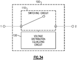
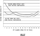
- a radio frequency switch circuit that includes: an antenna terminal; a first and second RF terminal; a first through transistor placed between the antenna terminal and the first RF terminal; a second through transistor placed between the antenna terminal and the second RF terminal; a first shunt transistor placed between ground and the first RF terminal; a second shunt transistor placed between the ground and the second RF terminal; and a distortion compensation circuit including a reverse parallel connected MOS capacitor whose capacitance around 0 volts has voltage dependence that is convex to the minus direction, the distortion compensation circuit being operable to compensate for voltage dependence of off-capacitance around 0 volts of the first and second through transistor and the first and second shunt transistor that is convex to the plus direction. Electrical connection between the antenna terminal and the first and second RF terminal is switchable.
- circuits that couple different portions of a field-effect transistor (FET) and/or different FETs to yield desirable performance improvements for RF switch systems.
- FET field-effect transistor
- one or more features of a given example can provide such performance improvements.
- features from different examples can be combined to yield such performance improvements.
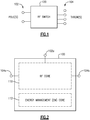
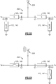
- FIG. 1 schematically shows a radio-frequency (RF) switch 100 configured to switch one or more signals between one or more poles 102 and one or more throws 104.
- RF radio-frequency
- a switch can be based on one or more field-effect transistors (FETs) such as silicon-on-insulator (SOI) FETs.
- FETs field-effect transistors
- SOI silicon-on-insulator
- Figure 2 shows that in some implementations, the RF switch 100 of Figure 1 can include an RF core 110 and an energy management (EM) core 112.
- the RF core 110 can be configured to route RF signals between the first and second ports.
- first and second ports can include a pole 102a and a first throw 104a, or the pole 102a and a second throw 104b.
- EM core 112 can be configured to supply, for example, voltage control signals to the RF core.
- the EM core 112 can be further configured to provide the RF switch 100 with logic decoding and/or power supply conditioning capabilities.
- the RF core 110 can include one or more poles and one or more throws to enable passage of RF signals between one or more inputs and one or more outputs of the switch 100.
- the RF core 110 can include a single-pole double-throw (SPDT or SP2T) configuration as shown in Figure 2 .
- Figure 3 shows a more detailed example configuration of an RF core 110.
- the RF core 110 is shown to include a single pole 102a coupled to first and second throw nodes 104a, 104b via first and second transistors (e.g., FETs) 120a, 120b.
- the first throw node 104a is shown to be coupled to an RF ground via an FET 122a to provide shunting capability for the node 104a.
- the second throw node 104b is shown to be coupled to the RF ground via an FET 122b to provide shunting capability for the node 104b.
- the FET 120a between the pole 102a and the first throw node 104a can be in an ON state
- the FET 120b between the pole 102a and the second throw node 104b can be in an OFF state.
- the shunt FETs 122a, 122b can be in an OFF state so that the RF signal is not shunted to ground as it travels from the pole 102a to the first throw node 104a.
- the shunt FET 122b associated with the second throw node 104b can be in an ON state so that any RF signals or noise arriving at the RF core 110 through the second throw node 104b is shunted to the ground so as to reduce undesirable interference effects to the pole-to-first-throw operation.
- the RF core can be configured with other numbers of poles and throws. For example, there may be more than one poles, and the number of throws can be less than or greater than the example number of two.
- the transistors between the pole 102a and the two throw nodes 104a, 104b are depicted as single transistors.
- switching functionalities between the pole(s) and the throw(s) can be provided by switch arm segments, where each switch arm segment includes a plurality of transistors such as FETs.
- FIG. 4 An example RF core configuration 130 of an RF core having such switch arm segments is shown in Figure 4 .
- the pole 102a and the first throw node 104a are shown to be coupled via a first switch arm segment 140a.
- the pole 102a and the second throw node 104b are shown to be coupled via a second switch arm segment 140b.
- the first throw node 104a is shown to be capable of being shunted to an RF ground via a first shunt arm segment 142a.
- the second throw node 104b is shown to be capable of being shunted to the RF ground via a second shunt arm segment 142b.
- the RF core 130 when the RF core 130 is in a state where an RF signal is being passed between the pole 102a and the first throw node 104a, all of the FETs in the first switch arm segment 140a can be in an ON state, and all of the FETs in the second switch arm segment 104b can be in an OFF state.
- the first shunt arm 142a for the first throw node 104a can have all of its FETs in an OFF state so that the RF signal is not shunted to ground as it travels from the pole 102a to the first throw node 104a.
- All of the FETs in the second shunt arm 142b associated with the second throw node 104b can be in an ON state so that any RF signals or noise arriving at the RF core 130 through the second throw node 104b is shunted to the ground so as to reduce undesirable interference effects to the pole-to-first-throw operation.
- a switch arm segment (e.g., 140a, 140b, 142a, 142b) can include one or more semiconductor transistors such as FETs.
- an FET may be capable of being in a first state or a second state and can include a gate, a drain, a source, and a body (sometimes also referred to as a substrate.
- an FET can include a metal-oxide-semiconductor field effect transistor (MOSFET).
- MOSFET metal-oxide-semiconductor field effect transistor
- one or more FETs can be connected in series forming a first end and a second end such that an RF signal can be routed between the first end and the second end when the FETs are in a first state (e.g., ON state).
- a first state e.g., ON state
- FIG. 5 schematically shows that in some implementations, such controlling of an FET 120 can be facilitated by a circuit 150 configured to bias and/or couple one or more portions of the FET 120.
- a circuit 150 can include one or more circuits configured to bias and/or couple a gate of the FET 120, bias and/or couple a body of the FET 120, and/or couple a source/drain of the FET 120.
- a switch arm segment 140 (that can be, for example, one of the example switch arm segments 140a, 140b, 142a, 142b of the example of Figure 4 ) between nodes 144, 146 is shown to include a plurality of FETs 120. Operations of such FETs can be controlled and/or facilitated by a gate bias/coupling circuit 150a, and a body bias/coupling circuit 150c, and/or a source/drain coupling circuit 150b.
- the gate of each of the FETs 120 can be connected to the gate bias/coupling circuit 150a to receive a gate bias signal and/or couple the gate to another part of the FET 120 or the switch arm 140.
- designs or features of the gate bias/coupling circuit 150a can improve performance of the switch arm 140. Such improvements in performance can include, but are not limited to, device insertion loss, isolation performance, power handling capability and/or switching device linearity.
- the body of each FET 120 can be connected to the body bias/coupling circuit 150c to receive a body bias signal and/or couple the body to another part of the FET 120 or the switch arm 140.
- designs or features of the body bias/coupling circuit 150c can improve performance of the switch arm 140. Such improvements in performance can include, but are not limited to, device insertion loss, isolation performance, power handling capability and/or switching device linearity.
- the source/drain of each FET 120 can be connected to the coupling circuit 150b to couple the source/drain to another part of the FET 120 or the switch arm 140.
- designs or features of the coupling circuit 150b can improve performance of the switch arm 140. Such improvements in performance can include, but are not limited to, device insertion loss, isolation performance, power handling capability and/or switching device linearity.
- a switching device performance parameter can include a measure of insertion loss.
- a switching device insertion loss can be a measure of the attenuation of an RF signal that is routed through the RF switching device. For example, the magnitude of an RF signal at an output port of a switching device can be less than the magnitude of the RF signal at an input port of the switching device.
- a switching device can include device components that introduce parasitic capacitance, inductance, resistance, or conductance into the device, contributing to increased switching device insertion loss.
- a switching device insertion loss can be measured as a ratio of the power or voltage of an RF signal at an input port to the power or voltage of the RF signal at an output port of the switching device. Decreased switching device insertion loss can be desirable to enable improved RF signal transmission.
- a switching device performance parameter can also include a measure of isolation.
- Switching device isolation can be a measure of the RF isolation between an input port and an output port an RF switching device. In some embodiments, it can be a measure of the RF isolation of a switching device while the switching device is in a state where an input port and an output port are electrically isolated, for example while the switching device is in an OFF state. Increased switching device isolation can improve RF signal integrity. In certain embodiments, an increase in isolation can improve wireless communication device performance.
- a switching device performance parameter can further include a measure of intermodulation distortion (IMD) performance.
- IMD intermodulation distortion
- IMD can be a measure of non-linearity in an RF switching device.
- IMD can result from two or more signals mixing together and yielding frequencies that are not harmonic frequencies. For example, suppose that two signals have fundamental frequencies f 1 and f 2 (f 2 > f 1 ) that are relatively close to each other in frequency space. Mixing of such signals can result in peaks in frequency spectrum at frequencies corresponding to different products of fundamental and harmonic frequencies of the two signals.
- a second-order intermodulation distortion (also referred to as IMD2) is typically considered to include frequencies f 1 +f 2 f 2 -f 1 , 2f 1 , and 2f 2 .
- a third-order IMD (also referred to as IMD3) is typically considered to include 2f 1 +f 2 , 2f 1 -f 2 , f 1 +2f 2 , f 1 -2f 2 . Higher order products can be formed in similar manners.
- Non linearity in RF systems can result in introduction of spurious signals into the system.
- Spurious signals in the RF system can result in interference within the system and degrade the information transmitted by RF signals.
- An RF system having increased non-linearity can demonstrate increased susceptibility to interference.
- Non-linearity in system components for example switching devices, can contribute to the introduction of spurious signals into the RF system, thereby contributing to degradation of overall RF system linearity and IMD performance.
- RF switching devices can be implemented as part of an RF system including a wireless communication system. IMD performance of the system can be improved by increasing linearity of system components, such as linearity of an RF switching device.
- a wireless communication system can operate in a multi-band and/or multi-mode environment. Improvement in intermodulation distortion (IMD) performance can be desirable in wireless communication systems operating in a multi-band and/or multi-mode environment. In some embodiments, improvement of a switching device IMD performance can improve the IMD performance of a wireless communication system operating in a multi-mode and/or multi-band environment.
- IMD intermodulation distortion
- Improved switching device IMD performance can be desirable for wireless communication devices operating in various wireless communication standards, for example for wireless communication devices operating in the LTE communication standard. In some RF applications, it can be desirable to improve linearity of switching devices operating in wireless communication devices that enable simultaneous transmission of data and voice communication. For example, improved IMD performance in switching devices can be desirable for wireless communication devices operating in the LTE communication standard and performing simultaneous transmission of voice and data communication (e.g., SVLTE).
- RF switching devices In some RF applications, it can be desirable for RF switching devices to operate under high power while reducing degradation of other device performance parameters. In some embodiments, it can be desirable for RF switching devices to operate under high power with improved intermodulation distortion, insertion loss, and/or isolation performance.
- an increased number of transistors can be implemented in a switch arm segment of a switching device to enable improved power handling capability of the switching device.
- a switch arm segment can include an increased number of FETs connected in series, an increased FET stack height, to enable improved device performance under high power.
- increased FET stack height can degrade the switching device insertion loss performance.
- a switching device can be implemented on-die, off-die, or some combination thereon.
- a switching device can also be fabricated using various technologies.
- RF switching devices can be fabricated with silicon or silicon-on-insulator (SOI) technology.
- an RF switching device can be implemented using silicon-on-insulator (SOI) technology.
- SOI technology can include a semiconductor substrate having an embedded layer of electrically insulating material, such as a buried oxide layer beneath a silicon device layer.
- an SOI substrate can include an oxide layer embedded below a silicon layer.
- Other insulating materials known in the art can also be used.
- SOI technology can enable reduced power consumption. Reduced power consumption can be desirable in RF applications, including those associated with wireless communication devices. SOI technology can enable reduced power consumption of device circuitry due to decreased parasitic capacitance of transistors and interconnect metallization to a silicon substrate. Presence of a buried oxide layer can also reduce junction capacitance or use of high resistivity substrate, enabling reduced substrate related RF losses. Electrically isolated SOI transistors can facilitate stacking, contributing to decreased chip size.
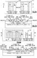
- each transistor can be configured as a finger-based device where the source and drain are rectangular shaped (in a plan view) and a gate structure extends between the source and drain like a rectangular shaped finger.
- Figures 7A and 7B show plan and side sectional views of an example finger-based FET device implemented on SOI.
- FET devices described herein can include a p-type FET or an n-type FET.
- FET devices are described herein as p-type devices, it will be understood that various concepts associated with such p-type devices can also apply to n-type devices.
- a pMOSFET can include an insulator layer formed on a semiconductor substrate.
- the insulator layer can be formed from materials such as silicon dioxide or sapphire.
- An n-well is shown to be formed in the insulator such that the exposed surface generally defines a rectangular region.
- Source (S) and drain (D) are shown to be p-doped regions whose exposed surfaces generally define rectangles. As shown, S/D regions can be configured so that source and drain functionalities are reversed.
- Figures 7A and 7B further show that a gate (G) can be formed on the n-well so as to be positioned between the source and the drain.
- the example gate is depicted as having a rectangular shape that extends along with the source and the drain.
- an n-type body contact is also shown. Formations of the rectangular shaped well, source and drain regions, and the body contact can be achieved by a number of known techniques.
- the source and drain regions can be formed adjacent to the ends of their respective upper insulator layers, and the junctions between the body and the source/drain regions on the opposing sides of the body can extend substantially all the way down to the top of the buried insulator layer.
- Such a configuration can provide, for example, reduced source/drain junction capacitance.
- an additional gate region can be provided on the side so as to allow, for example, an isolated P+ region to contact the Pwell.
- Figures 8A and 8B show plan and side sectional views of an example of a multiple-finger FET device implemented on SOI. Formations of rectangular shaped n-well, rectangular shaped p-doped regions, rectangular shaped gates, and n-type body contact can be achieved in manners similar to those described in reference to Figures 7A and 7B .
- the example multiple-finger FET device of Figures 8A and 8B can be made to operate such that a drain of one FET acts as a source of its neighboring FET.
- the multiple-finger FET device as a whole can provide a voltage-dividing functionality.
- an RF signal can be provided at one of the outermost p-doped regions (e.g., the leftmost p-doped region); and as the signal passes through the series of FETs, the signal's voltage can be divided among the FETs.
- the rightmost p-doped region can act as an overall drain of the multi-finger FET device.
- a plurality of the foregoing multi-finger FET devices can be connected in series as a switch to, for example, further facilitate the voltage-dividing functionality.
- a number of such multi-finger FET devices can be selected based on, for example, power handling requirement of the switch.
- biasing/coupling configurations can be implemented in SOI FET-based switch circuits. It will be understood that some of the example biasing/coupling configurations can be combined to yield a combination of desirable features that may not be available to the individual configurations. It will also be understood that, although described in the context of RF switching applications, one or more features described herein can also be applied to other circuits and devices that utilize FETs such as SOI FETs.
- switch-related performance features can contribute significantly to system-level performance of cellular devices.
- factors such as substrate-coupling (sometimes also referred to as substrate parasitics) and SOI-process can limit the performance achievable.
- Such a limitation in performance of SOI switches can be addressed by extensive substrate crosstalk reduction techniques such as capacitive guard rings, and/or trap rich or deep trench isolation techniques. Such techniques typically have associated with them undesirable features such as being expensive, requiring relatively large areas, and requiring additional process steps. Also, such technique can yield a desirable effect that is limited to an isolation feature.
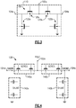
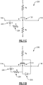
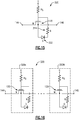
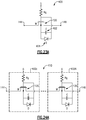
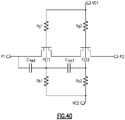
- Figure 9 shows a switch circuit 200 having an SOI FET 120 configured to provide switching functionality between first and second nodes 144, 146.
- a gate terminal of the FET 120 is shown to be biased by a bias voltage Vg provided by a gate bias circuit, and a body terminal of the FET 120 is shown to be biased by a bias voltage Vsb1 provided by a body bias circuit.
- the body terminal can be connected to a source terminal, so that both terminals are provided with the bias voltage Vsb1.
- the source terminal of the FET 120 can be connected to a non-linear capacitor 202.
- the capacitor 202 can be a MOSFET capacitor configured to provide one or more desired capacitance values.
- the MOS capacitor 202 can be configured to generate one or more harmonics to cancel or reduce non-linearity effects generated by the MOSFET 120.
- the MOS cap 202 is shown to be biased by Vsb2. In some embodiments, either or both of Vsb1 and Vsb2 can be adjusted to yield a desired level of non-linearity cancelation.
- Vsb1 and Vsb2 can be adjusted to yield a desired level of non-linearity cancelation.
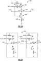
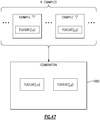
- Figure 10 shows a switch arm 210 having a plurality of the switch circuits 200 described in reference to Figure 9 .
- N such switch circuits are shown to be connected in series in a stack to provide switching functionality between terminals 144, 146.
- the number (N) of FETs in such a stack can be selected based on power being transferred between the terminals 144, 146. For example, N can be larger for situations involving higher power.
- gate bias voltages (Vg) for the plurality of FETs 120 can be substantially the same, and be provided by a common gate bias circuit. Such a common gate bias voltage Vg is shown to be provided to the gates via a gate resistor Rg.
- body bias voltages (Vsb1) for the plurality of FETs 120 can be substantially the same, and be provided by a common body bias circuit.
- body bias voltages (Vsb2) for the plurality of MOS capacitors 202 can be substantially the same, and be provided by a common body bias circuit (not shown).
- some or all of the bodies of the FETs 120 and/or the MOS capacitors 202 can be biased separately. Such a configuration can be beneficial in some situations, depending on the frequency of operation.
- the foregoing example configurations described in reference to Figures 9 and 10 can allow significant or substantially complete cancelation of non-linearity effects associated with one or more SOI FET based RF switches. In some embodiments, such configurations can be implemented so that minimal or relatively little additional area is required.
- Example 1 relates to a radio-frequency (RF) switch that includes at least one field-effect transistor (FET) disposed between first and second nodes, with each of the at least one FET having a respective source and drain.
- the switch further includes a compensation circuit connected to the respective source or the respective drain of each of the at least one FET.
- the compensation circuit is configured to compensate a non-linearity effect generated by the at least one FET.
- the FET can be a silicon-on-insulator (SOI) FET.
- the compensation circuit can include a non-linear capacitor.
- the non-linear capacitor can include a metal-oxide-semiconductor (MOS) capacitor.
- MOS capacitor can be configured to generate one or more harmonics to substantially cancel the non-linearity effect generated by the FET.
- the MOS capacitor can include an FET structure. The one or more harmonics generated by the MOS capacitor can be controlled at least in part by a body bias signal provided to the FET structure of the MOS capacitor.
- the non-linear capacitor can be connected to the source of the FET.
- the switch can further include a gate bias circuit connected to and configured to provide a bias signal to a gate of the FET.
- the switch can further include a body bias circuit connected to and configured to provide a bias signal to a body of the FET.
- the first node can be configured to receive an RF signal having a power value and the second node is configured to output the RF signal when the FET is in an ON state.
- the at least one FET can include N FETs connected in series, with the quantity N being selected to allow the switch circuit to handle the power of the RF signal.
- Example 1 relates to a method for operating a radio-frequency (RF) switch.
- the method includes controlling at least one field-effect transistor (FET) disposed between first and second nodes so that each of the at least one FET is in an ON state or an OFF state.
- the method further includes compensating a non-linear effect of the at least one FET by applying another non-linear signal to a respective source or a respective drain of each of the at least one FET.
- FET field-effect transistor
- Example 1 relates to a semiconductor die that includes a semiconductor substrate and at least one field-effect transistor (FET) formed on the semiconductor substrate.
- the die further includes a compensation circuit connected to a respective source or a respective drain of each of the at least one FET.
- the compensation circuit is configured to compensate a non-linearity effect generated by the at least one FET.
- the die can further include an insulator layer disposed between the FET and the semiconductor substrate.
- the die can be a silicon-on-insulator (SOI) die.
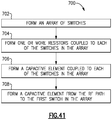
- Example 1 relates to a method for fabricating a semiconductor die.
- the method includes providing a semiconductor substrate, and forming at least one field-effect transistor (FET) on the semiconductor substrate, with each of the at least one FET having a respective source and a respective drain.
- the method further includes forming a compensation circuit on the semiconductor substrate.
- the method further includes connecting the compensation circuit to the respective source or the respective drain of each of the at least one FET to thereby allow the compensation circuit to compensate a non-linearity effect generated by the at least one FET.
- FET field-effect transistor
- the method can further include forming an insulator layer between the FET and the semiconductor substrate.
- Example 1 relates to a radio-frequency (RF) switch module that includes a packaging substrate configured to receive a plurality of components.
- the module further includes a semiconductor die mounted on the packaging substrate, with the die having at least one field-effect transistor (FET).
- FET field-effect transistor
- the module further includes a compensation circuit connected to a respective source or a respective drain of each of the at least one FET.
- the compensation circuit is configured to compensate a non-linearity effect generated by the at least one FET.
- the semiconductor die can be a silicon-on-insulator (SOI) die.
- compensation circuit can be part of the same semiconductor die as the at least one FET.
- the compensation circuit can be part of a second die mounted on the packaging substrate.
- the compensation circuit can be disposed at a location outside of the semiconductor die.
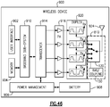
- Example 1 relates to a wireless device that includes a transceiver configured to process RF signals.
- the wireless device further includes an antenna in communication with the transceiver configured to facilitate transmission of an amplified RF signal.
- the wireless device further includes a power amplifier connected to the transceiver and configured to generate the amplified RF signal.
- the wireless device further includes a switch connected to the antenna and the power amplifier and configured to selectively route the amplified RF signal to the antenna.
- the switch includes at least one field-effect transistor (FET).
- FET field-effect transistor
- the switch further includes a compensation circuit connected to a respective source or a respective drain of each of the at least one FET.
- the compensation circuit is configured to compensate a non-linearity effect generated by the at least one FET.
- intermodulation distortion can be a measure of unwanted signal added to a desired signal due to mixing products from other radio-frequency (RF) signals.
- Such distortions can be particularly dominant in a multi-mode, multi-band environment.
- IMD can result from two or more signals mixing together and yielding frequencies that are not harmonic frequencies.
- susceptibility to such interference can be reduced by improving linearity of a system, since the system's linearity can govern how much IMD (and in turn interferences) will occur.
- improved linearity of the system's building blocks such as an RF switch
- an overall susceptibility of the system to interference can be decreased.
- LTE Long Term Evolution
- SVSTE simultaneous voice and data on LTE
- a gate terminal and either of source and drain terminals of an FET can be coupled by a circuit for IMD performance improvement.
- a circuit for IMD performance improvement it will be assumed that such a circuit couples the gate and source terminals; however, it will be understood that the circuit can couple the gate terminal and the drain terminal.
- a body terminal and either of source and drain terminals of an FET can be coupled by a circuit for IMD performance improvement.
- a circuit for IMD performance improvement it will be assumed that such a circuit couples the body and source terminals; however, it will be understood that the circuit can couple the body terminal and the drain terminal.
- each of gate and body terminal and either of source and drain terminals of an FET can be coupled by circuits for IMD performance improvement.
- circuits for IMD performance improvement it will be assumed that such circuits couple each of the gate and body terminals to the source terminal; however, it will be understood that such couplings can be made to the drain terminal.
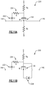
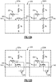
- Figures 11A-11F show switch circuit examples 220 having an SOI FET 120 configured to provide switching functionality between first and second nodes 144, 146.
- a gate terminal of the FET 120 is shown to be biased through a gate resistor Rg.
- the gate resistor Rg can be configured to float the gate.
- Figures 11A , 11C and 11E show configurations with a resistive-body connection (with a body resistor Rb, which can be configured to float the body); and
- Figures 11B , 11D and 11F show configurations with a diode-body connection (with a diode 226).
- either or both of gate and body terminals can be coupled with a source terminal by one or more coupling circuits having a capacitor 222 in series with a resistor 224.
- the coupling circuit is referred to as an RC circuit.
- Such a coupling can allow discharge of interface charge from the coupled gate and/or body. Such discharge of interface charge can lead to improvement in IMD performance, especially for low-frequency blocker.
- high impedance can be presented to the low-frequency signal by the RC circuit, which prevents it from leaking in to the gate, or reduces its leakage into the gate.
- high impedance can be presented to the low-frequency signal by the RC circuit, which prevents it from leaking in to the body, or reduces its leakage into the body.
- FIG 11A shows a switch circuit 220 where an RC circuit having a capacitor 222 (capacitance C) in series with a resistor 224 (resistance R) couples a source terminal with a gate terminal of an SOI FET 120.
- capacitor 222 capacitor 222
- resistor 224 resistor 224
- both of the gate and body are floated by their respective resistors Rg and Rb.
- FIG 11B shows a switch circuit 220 where an RC circuit having a capacitor 222 (capacitance C) in series with a resistor 224 (resistance R) couples a source terminal with a gate terminal of an SOI FET 120.
- the gate is floated by a resistor Rg, and a diode-body connection is provided.
- FIG 11C shows a switch circuit 220 where an RC circuit having a capacitor 222 (capacitance C) in series with a resistor 224 (resistance R) couples a source terminal with a body terminal of an SOI FET 120.
- capacitor 222 capacitor 222
- resistor 224 resistor 224
- both of the gate and body are floated by their respective resistors Rg and Rb.
- Figure 11D shows a switch circuit 220 where an RC circuit having a capacitor 222 (capacitance C) in series with a resistor 224 (resistance R) couples a source terminal with a body terminal of an SOI FET 120.
- the gate is floated by a resistor Rg, and a diode-body connection is provided.
- Figure 11E shows a switch circuit 220 where an RC circuit having a capacitor 222 (capacitance C) in series with a resistor 224 (resistance R) couples a source terminal with a body terminal of an SOI FET 120.
- Another RC circuit having a capacitor 222' (capacitance C') in series with a resistor 224' (resistance R') couples a source terminal with a gate terminal of the FET 120.
- both of the gate and body are floated by their respective resistors Rg and Rb.
- Figure 11F shows a switch circuit 220 where an RC circuit having a capacitor 222 (capacitance C) in series with a resistor 224 (resistance R) couples a source terminal with a body terminal of an SOI FET 120.
- Another RC circuit having a capacitor 222' (capacitance C') in series with a resistor 224' (resistance R') couples a source terminal with a gate terminal of the FET 120.
- the gate is floated by a resistor Rg, and a diode-body connection is provided.
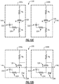
- FIGS 12A-12F show switch arms 230 having the switch circuits 220 described in reference to Figures 11A-11F .
- N such switch circuits are shown to be connected in series to provide switching functionality between terminals 144, 146.
- gate bias voltages (Vg) for the plurality of FETs 120 can be substantially the same, and be provided by a common gate bias circuit. Such a common gate bias voltage Vg is shown to be provided to the gates via a gate resistor Rg. Similarly, body bias voltages (Vb) for the plurality of FETs 120 can be substantially the same, and be provided by a common body bias circuit for the examples having resistive-body connection.
- some or all of the gates of the FETs 120 can be biased separately. In some situations, such as when substantially equal voltage division across the FETs is desired, it can be advantageous to implement such separate biasing of gates. Similarly, in some embodiments, some or all of the bodies of the FETs 120 can be biased separately. In some situations, such as when substantially equal voltage division across the FETs is desired, it can be advantageous to implement such separate biasing of bodies.
- Example 2 relates to a radio-frequency (RF) switch that includes at least one field-effect transistor (FET) disposed between first and second nodes, with each of the at least one FET having a respective source, drain, gate, and body.
- the RF switch further includes a coupling circuit having at least one of first and second paths, with the first path being between the respective source or the drain and the corresponding gate of each FET, and the second path being between the respective source or the drain and the corresponding body of each FET.
- the coupling circuit is configured to allow discharge of interface charge from either or both of the coupled gate and body.
- the FET can be a silicon-on-insulator (SOI) FET.
- the coupling circuit can include the first path but not the second path, with the coupling circuit including an RC circuit having a capacitor in series with a resistor to thereby allow the discharge from the gate.
- the coupling circuit can include the second path but not the first path, with the coupling circuit including an RC circuit having a capacitor in series with a resistor to thereby allow the discharge from the body.
- the coupling circuit can include both of the first and second paths, with the coupling circuit including first and second RC circuits.
- the first RC circuit can have a first capacitor in series with a first resistor to thereby allow the discharge from the gate.
- the second RC circuit can have a second capacitor in series with a second resistor to thereby allow the discharge from the body.
- each of the first and second paths can be connected to the drain.
- the RF switch can further include a gate resistor connected to the gate and configured to float the gate.
- the RF switch can further include a body resistor connected to the body and configured to float the body.
- the RF switch can further include a diode-body connection between the body and the gate.
- the first node can ge configured to receive an RF signal having a power value and the second node can be configured to output the RF signal when the FET is in an ON state.
- the at least one FET can include N FETs connected in series, with the quantity N being selected to allow the switch circuit to handle the power of the RF signal.
- Example 2 relates to a method for operating a radio-frequency (RF) switch.
- the method includes controlling at least one field-effect transistor (FET) disposed between first and second nodes.
- the method further includes discharging interface charge from at least one of a gate and a body of each FET by providing at least one of first and second paths, with the first path being between a source or a drain and the gate of each FET, and the second path being between the source or the drain and the body of each FET.
- FET field-effect transistor
- Example 2 relates to a semiconductor die that includes a semiconductor substrate and at least one field-effect transistor (FET) formed on the semiconductor substrate.
- the die further includes a coupling circuit having at least one of first and second paths, with the first path being between a source or a drain and a gate of each FET, and the second path being between the source or the drain and a body of each FET.
- the coupling circuit is configured to allow discharge of interface charge from either or both of the coupled gate and body.
- the coupling circuit can include at least one RC circuit having a capacitor in series with a resistor.
- the die can further include an insulator layer disposed between the FET and the semiconductor substrate.
- the die can be a silicon-on-insulator (SOI) die.
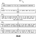
- Example 2 relates to a method for fabricating a semiconductor die.
- the method includes providing a semiconductor substrate and forming at least one field-effect transistor (FET) on the semiconductor substrate, with each of the at least one FETs having a respective gate, body, source, and drain.
- the method further includes forming a coupling circuit on the semiconductor substrate.
- the method further includes forming at least one of first and second paths with the coupling circuit, with the first path being between the respective source or the drain and the respective gate of each FET, and the second path being between the respective source or the drain and the respective body of each FET.
- the coupling circuit is configured to allow discharge of interface charge from either or both of the coupled gate and body.
- the method can further include forming an insulator layer between the FET and the semiconductor substrate.
- Example 2 relates to a radio-frequency (RF) switch module that includes a packaging substrate configured to receive a plurality of components.
- the module further includes a semiconductor die mounted on the packaging substrate, with the die having at least one field-effect transistor (FET).
- FET field-effect transistor
- the module further includes a coupling circuit having at least one of first and second paths, with the first path being between a source or a drain and a gate of each FET, and the second path being between the source or the drain and a body of each FET.
- the coupling circuit is configured to allow discharge of interface charge from either or both of the coupled gate and body.
- the semiconductor die can be a silicon-on-insulator (SOI) die.
- the coupling circuit can include at least one RC circuit having a capacitor in series with a resistor.
- the RC circuit can be part of the same semiconductor die as the at least one FET.
- at least some of the RC circuit can be part of a second die mounted on the packaging substrate.
- at least some of the RC circuit can be disposed at a location outside of the semiconductor die.
- Example 2 relates to a wireless device that includes a transceiver configured to process RF signals.
- the wireless device further includes an antenna in communication with the transceiver configured to facilitate transmission of an amplified RF signal.
- the wireless device further includes a power amplifier connected to the transceiver and configured to generate the amplified RF signal.
- the wireless device further includes a switch connected to the antenna and the power amplifier and configured to route the amplified RF signal to the antenna.
- the switch includes at least one field-effect transistor (FET).
- FET field-effect transistor
- the switch further includes a coupling circuit having at least one of first and second paths, with the first path being between a source or a drain and a gate of each FET, and the second path being between the source or the drain and a body of each FET.
- the coupling circuit is configured to allow discharge of interface charge from either or both of the coupled gate and body.
- the coupling circuit can include at least one RC circuit having a capacitor in series with a resistor.
- the wireless device can be configured to operate in an LTE communication system.
- Some wireless systems such as Long Term Evolution (LTE), Worldwide Interoperability for Microwave Access (WiMAx) and Code Division Multiple Access (CDMA) can demand very high linearity radio-frequency (RF) switches.
- RF switches can be implemented based on FETs such as SOI FETs.
- a challenge associated with such high linearity FET switches can include providing desired low frequency IMD2 and IMD3 performance specifications.
- an FET for such switches can behave like a MOS capacitor due to fixed charges in a body of the FET; and such a MOS capacitor can be highly nonlinear. Such an effect can be much more pronounced as lower frequencies.
- low-frequency IMD can be much more difficult to manage due to, for example. process limitations.
- Some solutions rely on a low pass filter at an antenna terminal. Other solutions utilize guard rings, trap rich or isolation deep trenches. These solutions can be relatively expensive, and typically require extra spacing and process steps.
- one or more of the foregoing challenges can be addressed by connecting a frequency-tuned circuit to a body of an FET.
- a frequency-tuned circuit can be connected to a body of an FET.
- such a circuit can be switched on or off. Accordingly, such a configuration can provide a dynamic way of controlling the body with a frequency dependent component.
- a frequency-tuned circuit can behave like a short circuit at low frequencies and like an open circuit at an operating frequency.
- Such a configuration can remove the fixed surface charges in the body at low frequencies, by effectively shorting the low-frequency distortions to an RF ground and at the same time not impacting the switching circuit behavior at the operating frequency.
- operating frequencies can include, for example, frequencies in a range from approximately 700 to 6,000 MHz.
- Low frequencies corresponding to such operating frequencies can include, for example, frequencies below approximately 200 MHz (e.g., 90 to 180 MHz).
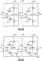
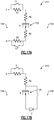
- Figure 13 shows a switch circuit example 300 having an SOI FET 120 configured to provide switching functionality between first and second nodes 144, 146.
- a gate terminal of the FET 120 is shown to be biased from a gate bias circuit.
- a body biasing circuit 302 can include an LC circuit having an inductor 308 (inductance L) and a capacitor 310 (capacitance C). Values of L and C can be selected to yield a desired resonance frequency of the LC circuit.
- the LC circuit is shown to be connectable to a ground by a switch 306 (e.g, another FET indicated as "M2"). Gate control of the FET M2 is shown to be provided by its gate bias voltage V_control through its gate resistor R.
- the switch 300 When the SOI FET 120 (indicated as "M1") is ON, the switch 300 is ON between the nodes 144 and 146, and M2 is turned OFF.
- This configuration can provide reduced or minimum insertion loss by floating the body of M1.
- M1 When M1 is OFF, the switch 300 is OFF between the nodes 144 and 146, and M2 is turned ON.
- This configuration can provide a DC short (as shown in the example of Figure 13 ) or a fixed DC voltage to the body substrate.
- this configuration can prevent or reduce the likelihood of parasitic junction diodes being turned on, and thereby reduce distortions associated with large voltage swings.
- the LC circuit can present high impedance and minimize the loading effect that can increase the insertion loss of the switch 300.
- Figure 14 shows a switch arm 310 having a plurality of the switch circuits 300 described in reference to Figure 14 .
- N such switch circuits are shown to be connected in series to provide switching functionality between terminals 144, 146.
- gate bias voltages (Vg) for the plurality of FETs 120 can be substantially the same, and be provided by a common gate bias circuit. Such a common gate bias voltage Vg is shown to be provided to the gates via a gate resistor Rg. In some embodiments, some or all of the gates of the FETs 120 can be biased separately. In some situations, such as when substantially equal voltage division across the FETs or when additional isolation between the FETs is desired, it can be advantageous to implement such separate biasing of gates.
- each switching circuit 300 is depicted as including a frequency-tuned body bias circuit.
- a common frequency tuned body bias circuit can provide a common bias connection for some or all of the FETs 120.
- some or all of the bodies of the FETs 120 can be biased separately. In some situations, such as when substantially equal voltage division across the FETs is desired, it can be advantageous to implement such separate biasing of bodies.
- the foregoing example configurations described in reference to Figures 13 and 14 can yield improvements at lower frequencies without significantly affecting the operating frequency performance.
- Another advantage that can be provided includes a feature where the body bias can be switched OFF to float the body when the switch is ON, thereby improving the insertion loss performance.
- Example 3 relates to a radio-frequency (RF) switch that includes at least one field-effect transistor (FET) disposed between first and second nodes, with each of the at least one FET having a respective body.
- the RF switch further includes a resonance circuit that connects the respective body of each FET to a reference node.
- the resonance circuit is configured to behave as an approximately closed circuit at low frequencies below a selected value and an approximately open circuit at an operating frequency, with the approximately closed circuit allowing removal of surface charge from the respective body to the reference node.
- the FET can be a silicon-on-insulator (SOI) FET.
- the resonance circuit can include an LC circuit having an inductor electrically parallel with a capacitor.
- the resonance circuit can further include a body switch configured to connect or disconnect the body to or from the reference node.
- the body switch can include a second FET.
- the second FET can be configured to be OFF when the first FET is ON to thereby float the body of the first FET.
- the second FET can be further configured to be ON when the first FET is OFF to facilitate the removal of surface charge from the body to the reference node.
- the reference node can include a ground node.
- the RF switch can further include a gate bias circuit connected to and configured to provide a bias signal to a gate of the FET.
- the first node can be configured to receive an RF signal having a power value and the second node can be configured to output the RF signal when the FET is in an ON state.
- the at least one FET can include N FETs connected in series, with the quantity N being selected to allow the switch circuit to handle the power of the RF signal.
- Example 3 relates to a method for operating a radio-frequency (RF) switch.
- the method includes controlling at least one field-effect transistor (FET) disposed between first and second nodes so that each of the at least one FET is in an ON state or an OFF state.
- the method further includes selectively removing surface charge from a respective body of each of the at least one FET at lower frequencies below a selected value. The selective removal is facilitated by a resonance circuit that behaves as an approximately closed circuit at the low frequencies.
- FET field-effect transistor
- the resonance circuit can further behave as an approximately open circuit at an operating frequency.
- the resonance circuit can include an LC circuit.
- Example 3 relates to a semiconductor die that includes a semiconductor substrate and at least one field-effect transistor (FET) formed on the semiconductor substrate.
- the die further includes a resonance circuit that connects a respective body of each of the at least one FET to a reference node.
- the resonance circuit is configured to behave as an approximately closed circuit at low frequencies below a selected value and as an approximately open circuit at an operating frequency. The approximately closed circuit allows removal of surface charge from the respective body to the reference node.
- the die can further include an insulator layer disposed between the FET and the semiconductor substrate.
- the die can be a silicon-on-insulator (SOI) die.
- Example 3 relates to a method for fabricating a semiconductor die.
- the method includes providing a semiconductor substrate and forming at least one field-effect transistor (FET) on the semiconductor substrate, with each of the at least one FET having a body.
- the method further includes forming a resonance circuit on the semiconductor substrate.
- the resonance circuit is configured to behave as an approximately closed circuit at low frequencies below a selected value and as an approximately open circuit at an operating frequency.
- the method further includes connecting the resonance circuit between the respective body of the at least one FET and a reference node to allow removal of surface charge from the respective body to the reference node when the resonance circuit is approximately closed.
- the method can further include forming an insulator layer between the FET and the semiconductor substrate.
- Example 3 relates to a radio-frequency (RF) switch module that includes a packaging substrate configured to receive a plurality of components.
- the module further includes a semiconductor die mounted on the packaging substrate, with the die having at least one field-effect transistor (FET).
- FET field-effect transistor
- the module further includes a resonance circuit that connects a respective body of each of the at least one FET to a reference node.
- the resonance circuit is configured to behave as an approximately closed circuit at low frequencies below a selected value and as an approximately open circuit at an operating frequency. The approximately closed circuit allows removal of surface charge from the respective body to the reference node.
- the semiconductor die can be a silicon-on-insulator (SOI) die.
- the resonance circuit can be part of the same semiconductor die as the at least one FET.
- the resonance circuit can be part of a second die mounted on the packaging substrate.
- the resonance circuit can be disposed at a location outside of the semiconductor die.
- Example 3 relates to a wireless device that includes a transceiver configured to process RF signals.
- the wireless device further includes an antenna in communication with the transceiver configured to facilitate transmission of an amplified RF signal.
- the wireless device further includes a power amplifier connected to the transceiver and configured to generate the amplified RF signal.
- the wireless device further includes a switch connected to the antenna and the power amplifier and configured to selectively route the amplified RF signal to the antenna.
- the switch includes at least one field-effect transistor (FET).
- FET field-effect transistor
- the switch further includes a resonance circuit that connects a respective body of each of the at least one FET to a reference node.
- the resonance circuit is configured to behave as an approximately closed circuit at low frequencies below a selected value and as an approximately open circuit at an operating frequency. The approximately closed circuit allows removal of surface charge from the respective body to the reference node.
- switch designs typically require high-power operation capability, especially under mismatch.
- switches used for antenna tuning are expected to withstand mismatch as high as 20:1 under +35 dBm input power.
- some switches utilized in wireless systems such as GSM are expected to withstand 5:1 mismatch under +35 dBm input power.
- Higher field-effect transistor (FET) stack height is generally used to withstand high power and improve the compression point.
- IMD intermodulation distortion
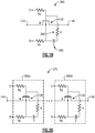
- Figure 15 shows a switch circuit example 320 having an SOI FET 120 configured to provide switching functionality between first and second nodes 144, 146.
- a gate terminal of the FET 120 can be biased through a gate resistor Rg.
- the switch circuit 320 can be implemented so that a body terminal of the FET 120 is utilized for power handling and IMD improvement.
- a circuit having a diode 322 in series with a resistor 324 (resistance R) can couple the body and gate of the FET 120.
- the anode of the diode 322 can be connected to the body of the FET 120, and the cathode can be connected to one of the resistor terminals.
- the other terminal of the resistor 324 is connected to the gate of the FET 120.
- Such a configuration can facilitate better distribution of excess charge from the body, which in turn can yield, for example, improvement in compression roll-off characteristics (e.g., higher P1dB) and IMD performance.
- the size of the diode 322 and the value of the resistor 324 can be selected to optimize or yield desirable performance associated with P1dB and IMD.
- Figure 16 shows a switch arm 330 having a plurality of the switch circuits 320 described in reference to Figure 15 .
- N such switch circuits are shown to be connected in series to provide switching functionality between terminals 144, 146.
- the number N can be selected based on power handling requirement. For example, N can be increased to handle higher power.
- gate bias voltages (Vg) for the plurality of FETs 120 can be substantially the same, and be provided by a common gate bias circuit. Such a common gate bias voltage Vg is shown to be provided to the gates via a gate resistor Rg. In some embodiments, some or all of the gates of the FETs 120 can be biased separately. In some situations, such as when substantially equal voltage division across the FETs is desired, it can be advantageous to implement such separate biasing of gates.
- a circuit having diode and resistor as described in reference to Figure 15 can be provided for each of the N individual switch circuits 320, can provide a common coupling between the N bodies and gates of the FETs, or any combination thereof.
- the diode(s) and resistor(s) described in reference to Figures 15 and 16 can be implemented on the same die as the switch circuit(s) 320, off of the die, or any combination thereof.
- this technique can improve compression roll-off characteristics of an RF switch (e.g., smooth roll-off).
- this technique can improve IMD performance of the RF switch.
- this technique can allow RF switch designs to eliminate resistive body contact topology which can require additional area overhead associated with, for example, body resistor, control lines and level shifters.
- Example 4 relates to a radio-frequency (RF) switch that includes at least one field-effect transistor (FET) disposed between first and second nodes, with each of the at least one FET having a respective body and gate.
- the RF switch further includes a coupling circuit that couples the respective body and gate of each FET.
- the coupling circuit includes a diode in series with a resistor and configured to facilitate removal of excess charge from the respective body.
- the FET can be a silicon-on-insulator (SOI) FET.
- SOI silicon-on-insulator
- an anode of the diode can be connected to the body, and a cathode of the diode can be connected to one end of the resistor with the other end of the resistor being connected to the gate.
- the diode and the resistor can be configured to yield improved P1dB and IMD performance of the switch.
- the RF switch can further include a gate resistor connected to the gate to facilitate floating of the gate.
- the first node can be configured to receive an RF signal having a power value and the second node can be configured to output the RF signal when the FET is in an ON state.
- the at least one FET can include N FETs connected in series, with the quantity N being selected to allow the switch circuit to handle the power of the RF signal.
- Example 4 relates to a method for operating a radio-frequency (RF) switch.
- the method includes controlling at least one field-effect transistor (FET) disposed between first and second nodes so that each FET is in an ON state or an OFF state.
- the method further includes removing excess charge from a body of each FET through a coupling circuit couples the body to a gate of the FET.
- the coupling circuit includes a diode in series with a resistor.
- Example 4 relates to a semiconductor die that includes a semiconductor substrate and at least one field-effect transistor (FET) formed on the semiconductor substrate.
- the die further includes a coupling circuit that couples a body and a gate of each FET.
- the coupling circuit includes a diode in series with a resistor and configured to facilitate removal of excess charge from the body of each FET.
- the die can further include an insulator layer disposed between the FET and the semiconductor substrate.
- the die can be a silicon-on-insulator (SOI) die.
- Example 4 relates to a method for fabricating a semiconductor die.
- the method includes providing a semiconductor substrate and forming at least one field-effect transistor (FET) on the semiconductor substrate, with each of the FET having a respective gate and body.
- the method further includes forming a coupling circuit on the semiconductor substrate.
- the coupling circuit includes a diode in series with a resistor.
- the method further includes connecting the coupling circuit between the body and the gate of each FET to facilitate removal of excess charge from the body.
- the method can further include forming an insulator layer between the FET and the semiconductor substrate.
- Example 4 relates to a radio-frequency (RF) switch module that includes a packaging substrate configured to receive a plurality of components.
- the module further includes a semiconductor die mounted on the packaging substrate, with the die having at least one field-effect transistor (FET).
- FET field-effect transistor
- the module further includes a coupling circuit that couples a body and a gate of each FET.
- the coupling circuit includes a diode in series with a resistor and configured to facilitate removal of excess charge from the body of each FET.
- the semiconductor die can be a silicon-on-insulator (SOI) die.
- the coupling circuit can be part of the same semiconductor die as the at least one FET.
- the coupling circuit can be part of a second die mounted on the packaging substrate.
- the coupling circuit can be disposed at a location outside of the semiconductor die.
- Example 4 relates to a wireless device that includes a transceiver configured to process RF signals.
- the wireless device further includes an antenna in communication with the transceiver configured to facilitate transmission of an amplified RF signal.
- the wireless device further includes a power amplifier connected to the transceiver and configured to generate the amplified RF signal.
- the wireless device further includes a switch connected to the antenna and the power amplifier and configured to selectively route the amplified RF signal to the antenna.
- the switch includes at least one field-effect transistor (FET).
- FET field-effect transistor
- the switch further includes a coupling circuit that couples a body and a gate of each FET.
- the coupling circuit includes a diode in series with a resistor and configured to facilitate removal of excess charge from the body of each FET.
- Intermodulation distortion measures an unwanted signal added to a desired signal due to mixing products from other RF signals. Such an effect can be particularly dominant in a multi-mode, multi-band environment. IMD can the result from two or more signals mixing together to yield frequencies that are not harmonic frequencies.
- Performance features such as a lower IMD in RF switches can be an important factor in wireless-device designs.
- Long Term Evolution (LTE) systems can benefit significantly from RF switches having reduced IMDs.
- system designs for simultaneous voice and data on LTE (SVLTE) can benefit significantly from RF switches having ultra-low levels of IMDs.
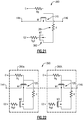
- Figure 17A shows a switch circuit example 340 having an SOI FET 120 configured to provide switching functionality between first and second nodes 144, 146.
- a gate of the FET 120 can be provided with a gate bias signal through a gate resistor (resistance Rg).
- a body of the FET 120 can be provided with a body bias signal through a body resistor (resistance Rb).
- extra gate and/or body resistance(s) can be provided for the FET 120.
- an extra gate resistor (resistance R1) is shown to be connected in series with the gate resistor Rg.
- such an extra gate resistance can be introduced in a selected manner by, for example, a switch S1 (e.g., another FET). For example, opening of the switch S1 results in the extra resistor R1 being in series with Rg; and closing of S1 results in the extra resistor R1 being bypassed when the extra resistance is not required or desired (e.g., for improved switching time).
- an extra body resistor (resistance R2) is shown to be connected in series with the body resistor Rb.
- an extra body resistance can be introduced in a selected manner by, for example, a switch S2 (e.g., another FET).
- a switch S2 e.g., another FET
- opening of the switch S2 results in the extra resistor R2 being in series with Rb; and closing of S2 results in the extra resistor R2 being bypassed when the extra resistance is not required or desired (e.g., for improved switching time).
- the extra resistances for the gate and the body can be turned ON or OFF together, or independently from each other. In some embodiments, only one of the extra resistances can be provided to the gate or the body.
- Figure 17B shows an example configuration 340 where an extra gate resistance is provided as described in reference to Figure 17A , but the body is configured with a diode (D) body contact.
- D diode
- Figures 18A and 18B show switch arms 350 having the switch circuits described in reference to Figures 17A and 17B .
- N switch circuits having gate resistance Rg and body resistance Rb are connected in series to provide switching functionality between terminals 144, 146.
- a common extra resistance R1 is shown to be provided to the gates of the FETs 120; and such an extra resistance R1 can be switched ON and OFF by a common switch S1.
- a common extra resistance R2 is shown to be provided to the bodies of the FETs 120; and such an extra resistance R2 can be switched ON and OFF by a common switch S2.
- such a switchable extra resistance can be provided separately to individual or some of the gates and/or bodies of the FETs in the switch arm 350.
- N switch circuits having gate resistance Rg and diode body contact are connected in series to provide switching functionality between terminals 144, 146.
- a common extra resistance R1 is shown to be provided to the gates of the FETs 120; and such an extra resistance R1 can be switched ON and OFF by a common switch S1.
- such a switchable extra resistance can be provided separately to individual or some of the gates and/or bodies of the FETs in the switch arm 350.
- the number (N) of switch circuits in the switch arm 350 can be selected based on power handling requirement. For example, N can be increased to handle higher power.
- the extra resistor(s) (R1 and/or R2) and their respective switch(es) described in reference to Figures 17 and 18 can be implemented on the same die as the switch circuit(s) 340, off of the die, or any combination thereof.
- values of the extra resistance(s) can be selected to optimize or improve IMD performance with minimal or reduced impact on switching time of the switch circuits 340.
- Such a configuration can yield improved IMD performance, including improvement for low-frequency blockers.
- the extra resistances (R1 and R2) can be selected to yield high impedances to low-frequency signals at the gate and body, thereby preventing or reducing such low-frequency signals from leaking into the gate and body.
- the foregoing example configurations described in reference to Figures 17 and 18 can be relatively simpler and easier to implement, and can yield a number of improvements.
- this technique can improve IMD performance of the RF switch, including IMD performance at low frequencies.
- Example 5 relates to a radio-frequency (RF) switch that includes at least one field-effect transistor (FET) disposed between first and second nodes, with each of the at least one FET having a respective gate and body.
- the RF switch further includes an adjustable-resistance circuit connected to at least one of the respective gate and body of each FET.
- the FET can be a silicon-on-insulator (SOI) FET.
- the adjustable-resistance circuit can include a first resistor in series with a parallel combination of a second resistor and a bypass switch. The bypass switch being closed can result in the second resistor being bypassed to yield a first resistance for the adjustable-resistance, and the bypass switch being open can result in a second resistance that is greater than the first resistance by approximately the value of the second resistor.
- the first resistor can include a bias resistor.
- the second resistance can be selected to improve intermodulation distortion (IMD) performance, and the first resistance can be selected to yield a reduced impact on switching time of the FET.
- IMD intermodulation distortion
- the adjustable-resistance circuit can be connected to the gate.
- the RF switch can further include a second adjustable-resistance circuit connected to the body.
- the RF switch can further include a diode body contact connected to the body.
- the adjustable-resistance circuit can be connected to the body but not the gate.
- the first node can be configured to receive an RF signal having a power value and the second node is configured to output the RF signal when the FET is in an ON state.
- the at least one FET can include N FETs connected in series, with the quantity N being selected to allow the switch circuit to handle the power of the RF signal.
- Example 5 relates to a method for operating a radio-frequency (RF) switch.
- the method includes controlling at least one field-effect transistor (FET) disposed between first and second nodes so that each FET is in an ON state or an OFF state.
- the method further includes adjusting a resistance of a circuit connected to at least one of gate and body of each FET.
- FET field-effect transistor
- the adjusting can include bypassing one of first and second resistors that are connected in series.
- Example 5 relates to a semiconductor die that includes a semiconductor substrate and at least one field-effect transistor (FET) formed on the semiconductor substrate.
- the die further includes an adjustable-resistance circuit connected to at least one of gate and body of each FET.
- FET field-effect transistor
- the die can further include an insulator layer disposed between the FET and the semiconductor substrate.
- the die can be a silicon-on-insulator (SOI) die.
- Example 5 relates to a method for fabricating a semiconductor die.
- the method includes providing a semiconductor substrate and forming at least one field-effect transistor (FET) on the semiconductor substrate, with each of the at least one FET having a respective gate and body.
- the method further includes forming an adjustable-resistance circuit on the semiconductor substrate.
- the method further includes connecting the adjustable-resistance circuit to at least one of the gate and the body of each FET.
- FET field-effect transistor
- the method can further include forming an insulator layer between the FET and the semiconductor substrate.
- Example 5 relates to a radio-frequency (RF) switch module that includes a packaging substrate configured to receive a plurality of components.
- the module further includes a semiconductor die mounted on the packaging substrate, with the die having at least one field-effect transistor (FET).
- FET field-effect transistor
- the module further includes an adjustable-resistance circuit connected to at least one of gate and body of each FET.
- the semiconductor die can be a silicon-on-insulator (SOI) die.
- the adjustable-resistance circuit can be part of the same semiconductor die as the at least one FET.
- the adjustable-resistance circuit can be part of a second die mounted on the packaging substrate.
- the adjustable-resistance circuit can be disposed at a location outside of the semiconductor die.
- Example 5 relates to a wireless device that includes a transceiver configured to process RF signals.
- the wireless device further includes an antenna in communication with the transceiver configured to facilitate transmission of an amplified RF signal.
- the wireless device further includes a power amplifier connected to the transceiver and configured to generate the amplified RF signal.
- the wireless device further includes a switch connected to the antenna and the power amplifier and configured to selectively route the amplified RF signal to the antenna.
- the switch includes at least one field-effect transistor (FET).
- FET field-effect transistor
- the switch further includes an adjustable-resistance circuit connected to at least one of gate and body of each FET.
- Intermodulation distortion measures an unwanted signal added to a desired signal due to mixing products from other RF signals. Such an effect can be particularly dominant in a multi-mode, multi-band environment. IMD can the result from two or more signals mixing together to yield frequencies that are not harmonic frequencies.
- Performance features such as a lower IMD in RF switches can be an important factor in wireless-device designs.
- Long Term Evolution (LTE) systems can benefit significantly from RF switches having reduced IMDs.
- system designs for simultaneous voice and data on LTE (SVLTE) can benefit significantly from RF switches having ultra-low levels of IMDs.
- Figure 19 shows a switch circuit example 360 having an SOI FET 120 configured to provide switching functionality between first and second nodes 144, 146.
- a gate terminal of the FET 120 can be biased through a gate resistor Rg to, for example, float the gate.
- a body terminal of the FET 120 can be biased through a body resistor Rb to, for example, float the body.
- the switch circuit 360 can be implemented to utilize a body terminal of the FET 120 to yield an improvement in IMD performance.
- an RC circuit that includes a capacitor 362 (capacitance C) in series with a resistor 364 (resistance R) can couple the body and gate of the FET 120. Such a coupling can allow discharge of interface charge from the body.
- values for capacitance C and resistance R can be selected to optimize or improve IMD performance of the switch circuit 360.
- Figure 20 shows a switch arm 370 having a plurality of the switch circuits 360 described in reference to Figure 19 .
- N such switch circuits are shown to be connected in series to provide switching functionality between terminals 144, 146.
- the number N can be selected based on power handling requirement. For example, N can be increased to handle higher power.
- gate bias voltages (Vg) for the plurality of FETs 120 can be substantially the same, and be provided by a common gate bias circuit. Such a common gate bias voltage Vg is shown to be provided to the gates via a gate resistor Rg. In some embodiments, some or all of the gates of the FETs 120 can be biased separately. In some situations, such as when substantially equal voltage division across the FETs is desired, it can be advantageous to implement such separate biasing of gates.
- a circuit having capacitor (capacitance C) and resistor (resistance R) as described in reference to Figure 19 can be provided for each of the N individual switch circuits 360, can provide a common coupling between the N bodies and gates of the FETs, or any combination thereof.
- capacitor(s) and resistor(s) described in reference to Figures 19 and 20 can be implemented on the same die as the switch circuit(s) 360, off of the die, or any combination thereof.
- the foregoing example configurations described in reference to Figures 19 and 20 can be relatively simpler and easier to implement, and can yield a number of improvements.
- this technique can improve IMD performance of the RF switch.
- this technique can provide improved roll-off characteristics for P1dB.
- Example 6 relates to a radio-frequency (RF) switch that includes at least one field-effect transistor (FET) disposed between first and second nodes, with each of the at least one FET having a respective body gate.
- the RF switch further includes a coupling circuit disposed between the respective body and gate of each FET. The coupling circuit is configured to allow discharge of interface charge from the respective body.
- FET field-effect transistor
- the FET can be a silicon-on-insulator (SOI) FET.
- the coupling circuit can include a capacitor in series with a resistor. The capacitor and the resistor can be selected to yield an improved intermodulation distortion (IMD) performance of the switch.
- IMD intermodulation distortion
- the RF switch can further include a gate bias resistor connected to the gate. In some embodiments, the RF switch can further include a body bias resistor connected to the body.
- the first node can be configured to receive an RF signal having a power value and the second node can be configured to output the RF signal when the FET is in an ON state.
- the at least one FET can include N FETs connected in series, with the quantity N being selected to allow the switch circuit to handle the power of the RF signal.
- Example 6 relates to a method for operating a radio-frequency (RF) switch.
- the method includes controlling at least one field-effect transistor (FET) disposed between first and second nodes so that the FET is in an ON state or an OFF state.
- the method further includes discharging interface charge from a respective body of each FET through a coupling circuit disposed between the respective body and a corresponding gate of the FET.
- FET field-effect transistor
- Example 6 relates to a semiconductor die that includes a semiconductor substrate and at least one field-effect transistor (FET) formed on the semiconductor substrate.
- the die further includes a coupling circuit disposed between a body and a gate of each FET.
- the coupling circuit is configured to allow discharge of interface charge from the body.
- the die can further include an insulator layer disposed between the FET and the semiconductor substrate.
- the die can be a silicon-on-insulator (SOI) die.
- Example 6 relates to a method for fabricating a semiconductor die.
- the method includes providing a semiconductor substrate and forming at least one field-effect transistor (FET) on the semiconductor substrate, with each of the at least one FET having a gate and body.
- the method further includes forming a coupling circuit on the semiconductor substrate that is connected to the respective body and gate of each FET to allow discharge of interface charge from the respective body.
- FET field-effect transistor
- the method can further include forming an insulator layer between the FET and the semiconductor substrate.
- the coupling circuit can include a capacitor in series with a resistor.
- Example 6 relates to a radio-frequency (RF) switch module that includes a packaging substrate configured to receive a plurality of components.
- the module further includes a semiconductor die mounted on the packaging substrate, with the die having at least one field-effect transistor (FET).
- FET field-effect transistor
- the module further includes a coupling circuit disposed between a body and a gate of each FET. The coupling circuit is configured to allow discharge of interface charge from the body.
- the semiconductor die can be a silicon-on-insulator (SOI) die.
- the coupling circuit can include a capacitor in series with a resistor.
- the coupling circuit can be part of the same semiconductor die as the at least one FET. In some embodiments, the coupling circuit can be part of a second die mounted on the packaging substrate. In some embodiments, the coupling circuit can be disposed at a location outside of the semiconductor die.
- Example 6 relates to a wireless device that includes a transceiver configured to process RF signals.
- the wireless device further includes an antenna in communication with the transceiver configured to facilitate transmission of an amplified RF signal.
- the wireless device further includes a power amplifier connected to the transceiver and configured to generate the amplified RF signal.
- the wireless device further includes a switch connected to the antenna and the power amplifier and configured to selectively route the amplified RF signal to the antenna.
- the switch includes at least one field-effect transistor (FET).
- FET field-effect transistor
- the switch further includes a coupling circuit disposed between a body and a gate of each FET. The coupling circuit is configured to allow discharge of interface charge from the body.
- switches having low insertion loss and high isolation values. High linearity of such switches is also desirable. As described herein, such advantageous performance features can be achieved without significantly degrading reliability of RF switches.
- Figure 21 shows a switch circuit example 380 having an SOI FET 120 configured to provide switching functionality between first and second nodes 144, 146.
- a gate of the FET 120 can be biased through a gate resistor Rg to, for example, float the gate.
- a body of the FET 120 is shown to be resistively coupled to the gate by a resistor 384 (resistance R), and such a coupling can be turned ON or OFF by a second FET 382 (indicated as M2). Operation of M2 can be controlled by a gate bias voltage provided to M2 through a gate resistor Rg2.
- the switch circuit 380 When the FET 120 (indicated as M1) is ON, the switch circuit 380 is ON, and M2 can be turned OFF. Such a configuration can provide minimum or reduced insertion loss of the switch circuit 380 by floating the body of M1. When M1 is OFF, the switch circuit 380 is OFF, and M2 can be turned ON. Such a configuration can provide DC voltages to both body gate of M1 from the same node (e.g. the gate node "G"). Such a configuration can prevent or reduce parasitic junction diodes being turned on, and can reduce distortions associated with large voltage swings. In some embodiments, such a configuration can also eliminate extra bias/control supply to the body of M1.
- Figure 22 shows a switch arm 390 having a plurality of the switch circuits 380 described in reference to Figure 21 .
- N such switch circuits are shown to be connected in series to provide switching functionality between terminals 144, 146.
- the number N can be selected based on power handling requirement. For example, N can be increased to handle higher power.
- gate bias voltages (Vg) for the plurality of FETs 120 can be substantially the same, and be provided by a common gate bias circuit. Such a common gate bias voltage Vg is shown to be provided to the gates via a gate resistor Rg. In some embodiments, some or all of the gates of the FETs 120 can be biased separately. In some situations, such as when substantially equal voltage division across the FETs is desired, it can be advantageous to implement such separate biasing of gates.
- a switchable (by M2) resistive coupling circuit between the body and gate of each FET 120 as described in reference to Figure 21 can be provided for each of the N individual switch circuits 380, can provide a common coupling between the N bodies and gates of the FETs, or any combination thereof.
- some or all of the bodies of the FETs 120 can be biased separately. In some situations, such as when substantially equal voltage division across the FETs is desired, it can be advantageous to implement such separate biasing of bodies.
- the second FET(s) and the resistor(s) described in reference to Figures 21 and 22 can be implemented on the same die as the switch circuit(s) 380, off of the die, or any combination thereof.
- this technique can provide minimum or reduced insertion loss of the switch circuit 380 or arm 390.
- this technique can prevent or reduce parasitic junction diodes being turned on, and can reduce distortions associated with large voltage swings.
- Example 7 relates to a radio-frequency (RF) switch that includes at least one first field-effect transistor (FET) disposed between first and second nodes, with each of the at least one first FETs having a respective body and gate.
- the RF switch further includes and a coupling circuit that couples the respective body and gate of each of the at least one first FET.
- the coupling circuit is configured to be switchable between a resistive-coupling mode and a body-floating mode.
- the first FET can be a silicon-on-insulator (SOI) FET.
- the coupling circuit can includes a resistance in series with a coupling switch.
- the coupling switch can include a second FET. The second FET can be OFF when the first FET is ON to yield the body-floating mode. The second FET can be ON when the first FET is OFF to yield the resistive-coupling mode.
- the RF switch can further include a gate bias resistor connected to the gate.
- the first node can be configured to receive an RF signal having a power value and the second node is configured to output the RF signal when the first FET is in an ON state.
- the at least one first FET can include N FETs connected in series, with the quantity N being selected to allow the switch circuit to handle the power of the RF signal.
- Example 7 relates to a method for operating a radio-frequency (RF) switch.
- the method includes controlling at least one field-effect transistor (FET) disposed between first and second nodes so that each of the at least one FET is in an ON state or an OFF state.
- the method further includes switching between a body-floating mode when each FET is ON and a resistive-coupling mode when each FET is OFF.
- FET field-effect transistor
- Example 7 relates to a semiconductor die that includes a semiconductor substrate and at least one field-effect transistor (FET) formed on the semiconductor substrate.
- the die further includes a coupling circuit that couples a respective body and gate of each of the at least one FET.
- the coupling circuit is configured to be switchable between a resistive-coupling mode and a body-floating mode.
- the die can further include an insulator layer disposed between the FET and the semiconductor substrate.
- the die can be a silicon-on-insulator (SOI) die.
- Example 7 relates to a method for fabricating a semiconductor die.
- the method includes providing a semiconductor substrate, and forming at least one field-effect transistor (FET) on the semiconductor substrate, with each of the at least one FET having a respective gate and body.
- the method further includes forming a coupling circuit on the semiconductor substrate.
- the method further includes connecting the coupling circuit with the respective body and gate of the at least one FET.
- the coupling circuit is configured to be switchable between a resistive-coupling mode and a body-floating mode.
- the method can further include forming an insulator layer between the FET and the semiconductor substrate.
- Example 7 relates to a radio-frequency (RF) switch module that includes a packaging substrate configured to receive a plurality of components, and a semiconductor die mounted on the packaging substrate, with the die having at least one field-effect transistor (FET).
- the switch module further includes a coupling circuit that couples a respective body and gate of each of the at least one FET.
- the coupling circuit is configured to be switchable between a resistive-coupling mode and a body-floating mode.
- the semiconductor die can be a silicon-on-insulator (SOI) die.
- the coupling circuit can be part of the same semiconductor die as the at least one FET.
- the coupling circuit can be part of a second die mounted on the packaging substrate.
- the coupling circuit can be disposed at a location outside of the semiconductor die.
- Example 7 relates to a wireless device that includes a transceiver configured to process RF signals, and an antenna in communication with the transceiver configured to facilitate transmission of an amplified RF signal.
- the wireless device further includes a power amplifier connected to the transceiver and configured to generate the amplified RF signal.
- the wireless device further includes a switch connected to the antenna and the power amplifier and configured to selectively route the amplified RF signal to the antenna.
- the switch includes at least one field-effect transistor (FET), and a coupling circuit that couples a respective body and gate of each of the at least one FET.
- the coupling circuit is configured to be switchable between a resistive-coupling mode and a body-floating mode.
- CMOS/SOI complementary metal-oxide-semiconductor/silicon-on-insulator
- pHEMT pseudomorphic high electron mobility transistor
- FIG 23A shows a switch circuit example 400 having an SOI FET 120 configured to provide switching functionality between first and second nodes 144, 146.
- a gate of the FET 120 can be biased through a gate resistor Rg to, for example, float the gate.
- a body of the FET 120 is shown to be coupled to the gate by a circuit having a capacitor 402 (capacitance C) arranged electrically parallel to a diode 404.
- the anode of the diode 404 is connected to the body of the FET 120, and the cathode of the diode 404 is connected to the gate of the FET 120.
- the diode 404 can be a PMOS diode, and the resulting parallel combination of the capacitor 402 and the PMOS diode can facilitate improvement of harmonic management, including IMD3 and IMD2.
- Figure 23B shows another example of a switch circuit 400 having an SOI FET 120 configured to provide switching functionality between first and second nodes 144, 146.
- a gate of the FET 120 can be biased through a gate resistor Rg to, for example, float the gate.
- a body of the FET 120 is shown to be coupled to the gate by a circuit having a capacitor 402 (capacitance C).
- the capacitor 402 can be utilized to couple the body and gate, but a separate body bias can be provided through a body resistor Rb. In some embodiments, such a body resistor can float the body.
- Figure 24A shows a switch arm 410 having a plurality of the switch circuits 400 described in reference to Figure 23A .
- Figure 24B shows a switch arm 410 having a plurality of the switch circuits 400 described in reference to Figure 23B .
- N such switch circuits are shown to be connected in series to provide switching functionality between terminals 144, 146.
- the number N can be selected based on power handling requirement. For example, N can be increased to handle higher power.
- gate bias voltages (Vg) for the plurality of FETs 120 can be substantially the same, and be provided by a common gate bias circuit. Such a common gate bias voltage Vg is shown to be provided to the gates via a gate resistor Rg. In some embodiments, some or all of the gates of the FETs 120 can be biased separately. In some situations, such as when substantially equal voltage division across the FETs is desired, it can be advantageous to implement such separate biasing of gates.
- a coupling circuit between the body and gate of each FET 120 as described in reference to Figures 23A and 23B can be provided for each of the N individual switch circuits 400.
- a common coupling between at least some of the N bodies and gates of the FETs can also be implemented.
- the capacitor and the diode described in reference to Figures 23 and 24 can be implemented on the same die as the switch circuit(s) 400, off of the die, or any combination thereof.
- the foregoing example configurations described in reference to Figures 23 and 24 can be relatively simpler and easier to implement, and can yield a number of improvements.
- the configurations of Figures 23A and 24A can be implemented without an extra external bias network.
- this technique can improve the IMD2 performance while also substantially maintaining the IMD3 performance.
- a resistance e.g., a resistor
- Such a configuration can help stabilize the voltage division across the FETs that are arranged in a stack.
- Figures 25A-25D show examples of simulation results demonstrating some of the advantageous features that can be provided by the RF switch configurations described in reference to Figures 23 and 24 .
- Figure 25A shows plots of simulated IMD2s versus phase shift for three example switch configurations.
- Plot 412a is for IMD2 of a standard switch without a capacitor.
- Plot 412b is for IMD2 of a standard switch with a capacitor (402 in Figure 23A ).
- Plot 412c is for IMD2 of a "TR" ("Trap Rich" configuration) switch with a capacitor (402 in Figure 23A ).
- the two switch configurations (412b, 412c) with capacitors are shown to have IMD2 values that are significantly improved of those of the no-capacitor configuration (412a) throughout the phase shift range.
- FIG 25A further shows plots of simulated IMD3s versus phase shift for the foregoing three example switch configurations.
- Plot 414a is for IMD3 of the standard switch without a capacitor.
- Plot 412b is for IMD3 of the standard switch with a capacitor (402 in Figure 23A ).
- Plot 412c is for IMD3 of the "TR" ("Trap Rich" configuration) switch with a capacitor (402 in Figure 23A ).
- TR Trap Rich
- Figures 25B-25D show plots of simulated harmonic distortions versus input power (P_in) in dBm.
- Figure 25B is a composite of second and third harmonics and gain for an example SP8T switch with a standard diode body bias ("w/o cap"), and with a diode-and-parallel-capacitor configuration ("w/ cap”).
- Figure 25C shows plots for the foregoing diode-and-parallel-capacitor configuration
- Figure 25D shows plots for the foregoing diode-only configuration.
- the second harmonic has values of approximately -34.5 dBm for the "w/o cap” case and approximately -48.4 dBm for the "w/ cap” case.
- the "w/o cap” case has a value of approximately -50.7 dBm
- the "w/ cap” case has a value of approximately -51.8 dBm.
- the "w/o cap” case has a value of approximately 0.536 dB
- the "w/ cap” case has a value of approximately 0.606 dB.
- Example 8 relates to a radio-frequency (RF) switch that includes at least one field-effect transistor (FET) disposed between first and second nodes, with each of the at least one FET having a respective body and gate.
- the RF switch further includes a coupling circuit that couples the respective body and gate of each FET.
- the coupling circuit includes a capacitor electrically parallel with a diode.
- the FET can be a silicon-on-insulator (SOI) FET.
- the coupling circuit can be configured to improve second-order intermodulation distortion (IMD2) performance without significantly degrading third-order intermodulation distortion (IMD3) performance.
- the diode can include a PMOS diode. An anode of the diode can be connected to the body and a cathode of the diode can be connected to the gate.
- the RF switch can further include a gate bias resistor connected to the gate.
- the first node can be configured to receive an RF signal having a power value and the second node can be configured to output the RF signal when the FET is in an ON state.
- the at least one FET can include N FETs connected in series, with the quantity N being selected to allow the switch circuit to handle the power of the RF signal.
- Example 8 relates to a method for operating a radio-frequency (RF) switch.
- the method includes controlling at least one field-effect transistor (FET) disposed between first and second nodes so that each of the at least one FET is in an ON state or an OFF state.
- the method further includes coupling a respective body and gate of each of the at least one FET through parallel combination of a capacitor and a diode.
- FET field-effect transistor
- Example 8 relates to a semiconductor die that includes a semiconductor substrate and at least one field-effect transistor (FET) formed on the semiconductor substrate.
- the die further includes a coupling circuit that couples a respective body and gate of each of the at least one FET.
- the coupling circuit includes a capacitor electrically parallel with a diode.
- the die further includes an insulator layer disposed between the FET and the semiconductor substrate.
- the die can be a silicon-on-insulator (SOI) die.
- Example 8 relates to a method for fabricating a semiconductor die.
- the method includes providing a semiconductor substrate and forming at least one field-effect transistor (FET) on the semiconductor substrate, with each of the at least one FET having a respective gate and body.
- the method further includes forming a coupling circuit on the semiconductor substrate that is between the respective body and gate of each FET.
- the coupling circuit includes a capacitor electrically parallel with a diode.
- the method can further include forming an insulator layer between the FET and the semiconductor substrate.
- Example 8 relates to a radio-frequency (RF) switch module that includes a packaging substrate configured to receive a plurality of components.
- the module further includes a semiconductor die mounted on the packaging substrate, with the die having at least one field-effect transistor (FET).
- FET field-effect transistor
- the module further includes a coupling circuit that couples a respective body and gate of each of the at least one FET.
- the coupling circuit includes a capacitor electrically parallel with a diode.
- the semiconductor die can be a silicon-on-insulator (SOI) die.
- the coupling circuit can be part of the same semiconductor die as the at least one FET.
- the coupling circuit can be part of a second die mounted on the packaging substrate.
- the coupling circuit can be disposed at a location outside of the semiconductor die.
- Example 8 relates to a wireless device that includes a transceiver configured to process RF signals.
- the wireless device further includes an antenna in communication with the transceiver configured to facilitate transmission of an amplified RF signal.
- the wireless device further includes a power amplifier connected to the transceiver and configured to generate the amplified RF signal.
- the wireless device further includes a switch connected to the antenna and the power amplifier and configured to selectively route the amplified RF signal to the antenna.
- the switch includes at least one field-effect transistor (FET).
- FET field-effect transistor
- the switch further includes a coupling circuit that couples a respective body and gate of each of the at least one FET.
- the coupling circuit includes a capacitor electrically parallel with a diode.
- Example 8 relates to a radio-frequency (RF) switch that includes at least one field-effect transistor (FET) disposed between first and second nodes, with each of the at least one FET having a respective body and gate.
- the RF switch further includes a coupling circuit that couples the respective body and gate of each FET.
- the coupling circuit includes a capacitor.
- the FET can be a silicon-on-insulator (SOI) FET.
- the coupling circuit can be configured to improve second-order intermodulation distortion (IMD2) performance without significantly degrading third-order intermodulation distortion (IMD3) performance.
- the RF switch can further include a gate bias resistor connected to the gate.
- the first node can be configured to receive an RF signal having a power value and the second node can be configured to output the RF signal when the FET is in an ON state.
- the at least one FET can include N FETs connected in series, with the quantity N being selected to allow the switch circuit to handle the power of the RF signal.
- a radio-frequency (RF) switch It is highly desirable for a radio-frequency (RF) switch to have low insertion loss, high isolation, and very high linearity. These performance parameters can usually conflict with each other. In some situations, these conflicting parameters can be dynamically adjusted by adjusting a gate bias resistor and a bias voltage for a body of a FET.
- a high value gate resistor In some situations, the foregoing challenge can be addressed with a high value gate resistor.
- a high value gate resistance being fixed can be problematic when the FET is in an OFF state, and when a signal needs to be shorted to a ground.
- a body bias can be applied to float the body when the FET is in an ON state, and grounded in an OFF state, to improve insertion loss, isolation, and linearity.
- FIG. 26 shows a switch circuit example 500 having an SOI FET 120 (also indicated as M1) configured to provide switching functionality between first and second nodes 144, 146.
- a gate of the FET 120 can be biased with Vctrl through a resistor R1 in a switchable manner by a second FET 502 (also indicated as M2) as described below.
- a body of the FET 120 is shown to be resistively coupled to a ground in a switchable manner by a third FET 506 (also indicated as M3) as also described below.
- Operation of M2 can be controlled by its gate bias voltage V_ctrl_comp provided to M2 through its gate resistor R2.
- Operation of M3 can be controlled by the same gate bias voltage Vctrl_comp provided to M3 without a gate resistor.
- M1 When the switch circuit 500 is ON, M1 is ON, and each of M2 and M3 can be turned OFF.
- Such a configuration can yield minimum or reduced insertion loss by floating the body and providing high impedance to the gate of M1 (e.g., by M2 behaving like a high value resistor when it is OFF).
- M1 When the switch circuit 500 is OFF, M1 is OFF, and each of M2 and M3 can be turned ON.
- Such a configuration can yield a ground bias to the body of M1 and an RF ground to the gate of M1, to thereby prevent or reduce the parasitic junction diode effects being turned on, and also reduce distortions associated with large voltage swings.
- the RF-shorting of M1's gate can also improve the isolation performance when M1 is OFF.
- FIG 27 shows a switch arm 510 having a plurality of the switch circuits 500 described in reference to Figure 26 .
- N such switch circuits are shown to be connected in series to provide switching functionality between terminals 144, 146.
- the number N can be selected based on power handling requirement. For example, N can be increased to handle higher power.
- a circuit that includes some or all of R1, R2, R3, M2 and M3 as described in reference to Figure 26 can be provided for each of the N individual switch circuits 500, can provided to all of the N switch circuits 500 as a common circuit, or any combination thereof.
- R1, R2, R3, M2 and M3 as described in reference to Figures 26 and 27 can be implemented on the same die as the switch circuit(s) 500, off of the die, or any combination thereof.
- the foregoing example configurations described in reference to Figures 26 and 27 can be relatively simpler and easier to implement, and can yield a number of improvements.
- this technique can provide minimum or reduced insertion loss when the switch circuit 500 or arm 510 is ON, and provide desirable features such as reduced parasitic junction diode effects, reduced distortions associated with large voltage swings, and improved isolation performance, when the switch circuit 500 or arm 510 is OFF.
- Example 9 relates to a radio-frequency (RF) switch that includes at least one field-effect transistor (FET) disposed between first and second nodes, with each of the at least one FET having a respective gate and body.
- the RF switch further includes a switchable resistive coupling circuit connected to the respective gate, and a switchable resistive grounding circuit connected to the corresponding body of the at least one FET.
- the FET can be a silicon-on-insulator (SOI) FET.
- the switchable resistive coupling circuit can include a bias resistor in series with a first coupling switch.
- the switchable resistive grounding circuit can include a body resistor in series with a second coupling switch.
- Each of the first and second coupling switches can be OFF when the FET is ON to yield a reduced insertion loss by floating the body and the gate.
- Each of the first and second coupling switches can be ON when the FET is OFF to yield a ground bias to the body and an RF ground to the gate, to thereby improve isolation performance of the RF switch.
- the first node can be configured to receive an RF signal having a power value and the second node can be configured to output the RF signal when the FET is in an ON state.
- the at least one FET can include N FETs connected in series, with the quantity N being selected to allow the switch circuit to handle the power of the RF signal.
- Example 9 relates to a method for operating a radio-frequency (RF) switch.
- the method includes controlling at least one field-effect transistor (FET) disposed between first and second nodes so that each of the at least one FET is in an ON state or an OFF state.
- the method further includes floating a respective gate and body of each of the at least one FET when each FET is in the ON state.
- the method further includes providing a ground bias to the respective body and an RF ground to the respective gate when each FET is in the OFF state.
- FET field-effect transistor
- Example 9 relates to a semiconductor die that includes a semiconductor substrate and at least one field-effect transistor (FET) formed on the semiconductor substrate.
- the die further includes a coupling circuit having a switchable resistive circuit connected to a respective gate of each of the at least one FET.
- the coupling circuit further includes a switchable resistive grounding circuit connected to a respective body of each of the at least one FET.
- the die can further include an insulator layer disposed between the FET and the semiconductor substrate.
- the die can be a silicon-on-insulator (SOI) die.
- Example 9 relates to a method for fabricating a semiconductor die.
- the method includes providing a semiconductor substrate.
- the method further includes forming at least one field-effect transistor (FET) on the semiconductor substrate, with each of the at least one FET having a respective gate and body.
- the method further includes forming a switchable resistive coupling circuit on the semiconductor substrate that is connected to the respective gate of the at least one FET.
- the method further includes forming a switchable resistive grounding circuit on the semiconductor substrate that is connected to the respective body of the at least one FET.
- FET field-effect transistor
- the method can further include forming an insulator layer between the FET and the semiconductor substrate.
- Example 9 relates to a radio-frequency (RF) switch module that includes a packaging substrate configured to receive a plurality of components.
- the module further includes a semiconductor die mounted on the packaging substrate, with the die having at least one field-effect transistor (FET).
- FET field-effect transistor
- the module further includes a coupling circuit having a switchable resistive circuit connected to a respective gate of each of the at least one FET.
- the coupling circuit further includes a switchable resistive grounding circuit connected to a respective body of each of the at least one FET.
- the semiconductor die can be a silicon-on-insulator (SOI) die.
- the coupling circuit can be part of the same semiconductor die as the at least one FET.
- the coupling circuit can be part of a second die mounted on the packaging substrate.
- the coupling circuit can be disposed at a location outside of the semiconductor die.
- Example 9 relates to a wireless device that includes a transceiver configured to process RF signals.
- the wireless device further includes an antenna in communication with the transceiver configured to facilitate transmission of an amplified RF signal.
- the wireless device further includes a power amplifier connected to the transceiver and configured to generate the amplified RF signal.
- the wireless device further includes a switch connected to the antenna and the power amplifier and configured to selectively route the amplified RF signal to the antenna.
- the switch includes at least one field-effect transistor (FET).
- the switch further includes a coupling circuit having a switchable resistive circuit connected to a respective gate of each of the at least one FET and a switchable resistive grounding circuit connected to a respective body of each of the at least one FET.
- switch designs typically require high-power operation capability, especially under mismatch.
- switches used for antenna tuning are expected to withstand mismatch as high as 20:1 under +35 dBm input power.
- some switches utilized in wireless systems such as GSM are expected to withstand 5:1 mismatch under +35 dBm input power.
- Higher field-effect transistor (FET) stack height is generally used to withstand high power under mismatch.
- FET field-effect transistor
- Figure 28 shows an example configuration of an FET stack 520 configured to provide switching of RF signals between first and second nodes 144, 146.
- the first and second nodes 144, 146 can be, for example, RF input and RF output, respectively.
- the stack 520 can include N SOI FETs (indicated as M1, M2, ..., MN) connected in series between the nodes 144, 146.
- the number N can be selected based on power handling requirement. For example, N can be increased to handle higher power.
- each gate of the FET is shown to be biased through a gate resistor Rg.
- N such gate resistors corresponding to the N FETs are shown to be connected to a common gate bias voltage source "G.”
- each body of the FET is shown to be biased through a body resistor Rb.
- N such body resistors corresponding to the N FETs are shown to be connected to a common body bias voltage source "B.”
- some or all of the gates of the FETs can be voltage-compensated to yield an improved voltage distribution across each FET in the stack 520. Such an improved voltage distribution can result in improvement in compression point, harmonics, and or IMD performance.
- the foregoing voltage-compensation of the gates can be achieved by coupling the gates of the FETs with capacitive elements Cgg (e.g., capacitors).
- Cgg1 couples the gates of M1 and M2
- Cgg2 couples the gates of M2 and M3, and so on, with Cgg(N-2) coupling the gates of M(N-2) and M(N-1), and Cgg(N-1) coupling the gates of M(N-1) and MN.
- the coupling capacitive elements Cgg can have substantially the same value.
- the capacitive elements Cgg can be scaled and/or optimized within the stack 520 with different values for Cgg1, Cgg2, Cgg3, etc. An example of such scaling of Cgg values to obtain a desired result is described in greater detail in reference to Figure 31 .
- a feed-forward capacitor, Cfwd can be provided to couple source/drain and gate of an end FET (e.g., M1). In some embodiments, the feed-forward capacitor Cfwd can couple source/drain and gate of a non-end FET within the FET stack. The feed-forward capacitor, Cfwd can ensure that the RF signal path between the nodes 144, 146 is coupled to at least one of the gates of the FETs.
- FIG 29 shows that in some implementations, voltage-compensation of the gates can be achieved by coupling the gates of the FETs with resistive elements Rgg (e.g., resistors).
- Rgg1 couples the gates of M1 and M2
- Rgg2 couples the gates of M2 and M3, and so on, with Rgg(N-2) coupling the gates of M(N-2) and M(N-1), and Rgg(N-1) coupling the gates of M(N-1) and MN.
- a feed-forward coupling between source/drain and gate of an FET e.g., M1 is shown to include a capacitor Cfwd in series with a resistor Rfwd.
- the coupling resistive elements Rgg can have substantially the same value. In some embodiments, the resistive elements Rgg can have different values that are selected to achieve a desired result.
- FIG. 30 shows that in some implementations, voltage-compensation of the gates can be achieved by coupling the gates of the FETs with capacitive elements Cgg (e.g., capacitors) and resistive elements Rgg (e.g., resistors).
- Cgg1 and Rgg1 in series couples the gates of M1 and M2
- Cgg2 and Rgg2 in series couples the gates of M2 and M3, and so on, with Cgg(N-2) and Rgg(N-2) in series coupling the gates of M(N-2) and M(N-1), and Cgg(N-1) and Rgg(N-1) in series coupling the gates of M(N-1) and MN.
- a feed-forward coupling between source/drain and gate of an FET e.g., M1 is shown to include a capacitor Cfwd in series with a resistor Rfwd.
- the coupling capacitive elements Cgg can have substantially the same value. In some embodiments, the capacitive elements Cgg can have different values that are selected to achieve a desired result. Similarly, the coupling resistive elements Rgg can have substantially the same value, or have different values selected to achieve a desired result.
- Figure 31 shows plots of voltage swings across each of the FETs in an example stack having 16 FETs.
- the "baseline” configuration corresponds to a stack where the gates are not voltage-compensated.
- the "gate compensation” configuration corresponds to a stack where the gates are voltage-compensated as described in reference to Figure 28 .
- the values of Cgg are selected as Cgg1 > Cgg2 > Cgg3 > ... > CggN. Voltage swings associated with such a configuration are shown to be significantly less than the baseline case.
- the capacitive elements Cgg described in reference to Figures 28 and 30 can be implemented on the same die as the FETs (M1, M2, etc.), off of the die, or any combination thereof.
- Such on-die and/or off-die implementations of the capacitive elements Cgg can include, for example, MIM capacitors and/or capacitive metal traces.
- the resistive elements Rgg described in reference to Figures 29 and 30 can be implemented on the same die as the FETs (M1, M2, etc.), off of the die, or any combination thereof.
- the foregoing example configurations described in reference to Figures 28-31 can be relatively simpler and easier to implement, and can yield a number of improvements.
- this technique can provide less fluctuations in voltage swings across each FET in a switch stack.
- Such a feature can yield other desirable features such as improved compression point, as well as improved harmonics and IMD performance.
- various example configurations related to gate-to-gate compensation can be combined with one or more features that can improve performance of one or more of the FETs in a given stack.
- Example 10 relates to a radio-frequency (RF) switch that includes a plurality of field-effect transistors (FETs) connected in series between first and second nodes, with each FET having a gate.
- the RF switch further includes a compensation network having a coupling circuit that couples the gates of each pair of neighboring FETs.
- the FETs can be silicon-on-insulator (SOI) FETs.
- the compensation network can be configured to reduce voltage swings across each of the plurality of FETs.
- the switch can further include a feed-forward circuit that couples a source of an end FET to the gate of the end FET.
- the feed-forward circuit can include a capacitor.
- the feed-forward circuit can further include a resistor in series with the capacitor.
- the coupling circuit can include a capacitor.
- the capacitors can have successively smaller capacitance values as the FETs are traversed from the first node to the second node.
- the coupling circuit can further include a resistor in series with the capacitor.
- the coupling circuit can include a resistor.
- the switch can further include a gate bias network connected to and configured to provide bias signals to the gates of the FETs.
- the gate bias network can be configured so that all of the gates receive a common bias signal.
- the switch can further include a body bias network connected to and configured to provide bias signals to the bodies of the FETs.
- the body bias network can be configured so that all of the bodies receive a common bias signal.
- the first node can be configured to receive an RF signal having a power value and the second node can be configured to output the RF signal when the FET is in an ON state.
- the at least one FET can include N FETs connected in series, with the quantity N being selected to allow the switch circuit to handle the power of the RF signal.
- Example 10 relates to a method for operating a radio-frequency (RF) switch.
- the method includes controlling a plurality of field-effect transistors (FETs) connected in series between first and second nodes so that the FETs are collectively in an ON state or an OFF state, with each FET having a gate.
- the method further includes coupling the gates of each of neighboring FETs to reduce voltage swings across each of the plurality of FETs.
- Example 10 relates to a semiconductor die that includes a semiconductor substrate and a plurality of field-effect transistors (FETs) formed on the semiconductor substrate and connected in series, with each FET having a gate.
- the die further includes a compensation network formed on the semiconductor substrate, the compensation network including a coupling circuit that couples the gates of each pair of neighboring FETs.
- the die can further include an insulator layer disposed between the FETs and the semiconductor substrate.
- the die can be a silicon-on-insulator (SOI) die.
- Example 10 relates to a method for fabricating a semiconductor die.
- the method includes providing a semiconductor substrate and forming a plurality of field-effect transistors (FETs) on the semiconductor substrate so as to be connected in series, with each FET having a gate.
- the method further includes forming a coupling circuit on the semiconductor substrate so as to couple the gates of each pair of neighboring FETs.
- FETs field-effect transistors
- the method can further include forming an insulator layer between the FETs and the semiconductor substrate.
- Example 10 relates to a radio-frequency (RF) switch module that includes a packaging substrate configured to receive a plurality of components.
- the module further includes a semiconductor die mounted on the packaging substrate.
- the die includes a plurality of field-effect transistors (FETs) connected in series, with each FET having a gate.
- the module further includes a compensation network having a coupling circuit that couples the gates of each pair of neighboring FETs.
- FETs field-effect transistors
- the semiconductor die can be a silicon-on-insulator (SOI) die.
- the compensation network can be part of the same semiconductor die as the at least one FET.
- the compensation network can be part of a second die mounted on the packaging substrate.
- the compensation network can be disposed at a location outside of the semiconductor die.
- Example 10 relates to a wireless device that includes a transceiver configured to process RF signals.
- the wireless device further includes an antenna in communication with the transceiver configured to facilitate transmission of an amplified RF signal.
- the wireless device further includes a power amplifier connected to the transceiver and configured to generate the amplified RF signal.
- the wireless device further includes a switch connected to the antenna and the power amplifier and configured to selectively route the amplified RF signal to the antenna.
- the switch includes a plurality of field-effect transistors (FETs) connected in series, with each FET having a gate.
- the switch further includes a compensation network having a coupling circuit that couples the gates of each pair of neighboring FETs.
- FETs field-effect transistors
- Intermodulation distortion measures an unwanted signal added to a desired signal due to mixing products from other RF signals. Such an effect can be particularly dominant in a multi-mode, multi-band environment. IMD can the result from two or more signals mixing together to yield frequencies that are not harmonic frequencies.
- Performance features such as a lower IMD in RF switches can be an important factor in wireless-device designs.
- Long Term Evolution (LTE) systems can benefit significantly from RF switches having reduced IMDs.
- system designs for simultaneous voice and data on LTE (SVLTE) can benefit significantly from RF switches having ultra-low levels of IMDs.
- Figure 32 shows a switching configuration 250 in an example context of a single-pole-dual-throw (SPDT) application.
- the single pole is shown to be connected to an antenna 252.
- One of the two throws is shown to be coupled to a receive (Rx) port via a switch circuit S.
- the Rx port can be coupled to a ground via a shunt switch circuit.
- the other throw is shown to be coupled to a transmit (Tx) port via a switch circuit S.
- the Tx port can be coupled to the ground via a shunt switch circuit.
- each of the switch circuits can include one or more FETs such as SOI FETs.
- FETs such as SOI FETs.
- a single FET is sometimes referred to herein with a reference numeral 120 or 122, and a stack of such FETs is sometimes referred to herein with a reference numeral 140 or 142.
- the "S" and “Shunt” switches can include one or more features described herein to provide various advantageous functionalities.
- the switching configuration of Figure 32 is shown to include capacitors to inhibit a low-frequency blocker from mixing with a fundamental frequency.
- a capacitor C1 is provided between the antenna node and the switch arm S of the Tx throw.
- a capacitor C2 is provided between the antenna node and the switch arm S of the Rx throw.
- a capacitor C3 is provided between the Tx node and its shunt switch arm.
- a capacitor C4 is provided between the Rx node and its shunt switch arm.
- a shunt arm may or may not be provided for the Rx node.
- Figure 33 shows an example operating configuration where some of the foregoing capacitors can provide desirable switching functionalities.
- the switching configuration is in a transmit mode. Accordingly, the transmit switch arm is ON (closed), and the receive switch arm is OFF (open). The shunt arm for the Tx node is OFF (open).
- capacitors C1-C4 described in reference to Figures 32 and 33 can be implemented on the same die as their respective switch circuits, off of the die, or any combination thereof.
- the foregoing example configurations described in reference to Figures 32 and 33 can be relatively simpler and easier to implement, and can yield a number of improvements.
- this technique can provide improved IMD performance by preventing a low-frequency blocker signal from mixing with a fundamental frequency signal.
- Example 11 relates to a radio-frequency (RF) switch system that includes a switch having a stack of field-effect transistors (FETs) connected in series between first and second nodes.
- the system further includes a capacitor connected in series with the switch and configured to inhibit a low-frequency blocker signal from mixing with a fundamental-frequency signal in the switch.
- FETs field-effect transistors
- the FETs can be silicon-on-insulator (SOI) FETs.
- the first node can be an antenna node.
- the capacitor can be disposed between the switch and the antenna node.
- the switch can be part of a transmit path such that the second node of the switch is an input node for an amplified RF signal.
- the switch can be part of a receive path such that the second node of the switch is an output node for an RF signal received from the antenna.
- Example 11 relates to a semiconductor die having a semiconductor substrate and a switch formed on the semiconductor substrate and having a stack of field-effect transistors (FETs) connected in series.
- the die further includes a capacitor formed on the semiconductor substrate and connected in series with the switch. The capacitor is configured to inhibit a low-frequency blocker signal from mixing with a fundamental-frequency signal in the switch.
- the die can further include an insulator layer disposed between the FETs and the semiconductor substrate.
- the die can be a silicon-on-insulator (SOI) die.
- Example 11 relates to a method for fabricating a semiconductor die.
- the method includes providing a semiconductor substrate and forming a stack of field-effect transistors (FETs) on the semiconductor substrate so as to be connected in series.
- the method further includes forming a capacitor on the semiconductor substrate so as to be connected in series with an end of the stack.
- the capacitor is configured to inhibit a low-frequency blocker signal from mixing with a fundamental-frequency signal in the stack.
- the method can further include forming an insulator layer between the FETs and the semiconductor substrate.
- Example 11 relates to a radio-frequency (RF) switch module that includes a packaging substrate configured to receive a plurality of components.
- the module further includes a semiconductor die mounted on the packaging substrate.
- the die includes a switch having a stack of field-effect transistors (FETs) connected in series.
- the module further includes a capacitor connected in series with the switch. The capacitor is configured to inhibit a low-frequency blocker signal from mixing with a fundamental-frequency signal in the switch.
- FETs field-effect transistors
- the semiconductor die can be a silicon-on-insulator (SOI) die.
- the capacitor can be part of the same semiconductor die as the FETs.
- the capacitor can be part of a second die mounted on the packaging substrate.
- the capacitor circuit can be disposed at a location outside of the semiconductor die.
- Example 11 relates to a wireless device that includes a transceiver configured to process RF signals.
- the wireless device further includes an antenna in communication with the transceiver.
- the wireless device further includes a switch module interconnected to the antenna and the transceiver and configured to selectively route RF signals to and from the antenna.
- the switch module includes a switch having a stack of field-effect transistors (FETs) connected in series.
- FETs field-effect transistors
- the switch module further includes a capacitor connected in series with the switch. The capacitor is configured to inhibit a low-frequency blocker signal from mixing with a fundamental-frequency signal in the switch.
- body-to-body compensation techniques can be applied to a stack of FETs such as SOI FETs. Such techniques can provide, for example, less fluctuations in voltage swings across each FET in a switch stack. Such a feature can yield other desirable features such as improved compression point, as well as improved harmonics and IMD performance.
- GSM switches may operate under 35dBm with 5:1 mismatch and switches used in antenna tuning may operate under 35 dBm with mismatch as high as 20:1.
- transmit switches operating under high power may experience uneven voltage distribution across the switch.
- Non-uniform voltage swing across a switch may produce adverse effects in device performance, including harmonic peaking, degradation in compression point and intermodulation distortion (IMD) performance of the switch.
- IMD intermodulation distortion
- circuits, devices and methodologies for providing more uniform voltage swing across a transmit switch for improved device performance are described herein.
- increased uniformity in voltage swing across a transmit switch may result in improved compression point, harmonics and intermodulation distortion performance.
- a switching device may be capable of being in a first state or a second state, such that the switching device may permit the transmission of RF signals between a first port and a second port while in one of the states. For example, when in a first state, such as an ON state, the RF switching device may enable transmission of RF signals from one port, such as an input port, to a second port, such as an output port. When in a second state, such as an OFF state, the RF switching device may prevent transmission of RF signals from an input port to an output port, thereby electrically isolating the input port from the output port.
- a first state such as an ON state
- the RF switching device may enable transmission of RF signals from one port, such as an input port, to a second port, such as an output port.
- a second state such as an OFF state
- the RF switching device may prevent transmission of RF signals from an input port to an output port, thereby electrically isolating the input port from the output port.
- a switching device 10 having a first port and a second port may include a switching circuit 11.
- the switching circuit 11 may further include a voltage distribution equalizing circuit 12.
- a voltage distribution equalizing circuit 12 may enable more uniform voltage distribution across a switching circuit 11 when the switching circuit is in an ON state, where an RF signal can be transmitted between an input port and an output port.
- a voltage distribution equalizing circuit 12 may improve voltage distribution across a switching circuit 11 operating under high power. Increased uniformity in voltage swing across a switching circuit 11 may enable improved switching device 10 performance, including improvement in compression point, harmonics and intermodulation distortion performance.
- a switching device 10 may be implemented on a semiconductor substrate.
- a switching device 10 may include a switching circuit 11 having an FET stack.
- an FET stack may include one or more FETs, where an FET has a source, a drain, a body node or a gate node. Additional FETs may be connected in series so as to define an RF signal path between an input end and an output end.
- the FET stack is capable of being in a first or second state, such that when in a first state, for example an ON state, an RF signal can be transmitted from the input end to the output end, allowing the switching device 10 to transmit an RF signal from an input port to an output port.
- FIG. 35 shows an example switching circuit having an FET stack that includes five FETs, FET1, FET2, FET3, FET4, and FET5, connected in series and defining an input end and an output end.
- Increasing the FET stack height, or the number of FETs, of a switching circuit may improve switching device performance, including performance while operating under high power.
- a switching device may exhibit non-uniform voltage distribution across the switching device FET stack when the switching device is in an ON state and encountered by an RF signal at its input port.
- a switching device may exhibit non-uniform voltage distribution across the switching device FET stack while operating under high power.
- Non-uniform voltage swing across an FET stack may adversely affect device performance, including harmonic peaking, intermodulation distortion (IMD), or compression point degradation.
- IMD intermodulation distortion
- a voltage distribution equalizing circuit may be coupled to a switching circuit to improve voltage swing uniformity across the switching circuit.
- a switching circuit having an FET stack may include a voltage distribution equalizing circuit that utilizes the body nodes of body contacted FETs for voltage compensation, thereby improving voltage distribution uniformity, or reducing voltage distribution variation, across the FET stack.
- the voltage distribution equalizing circuit may include a body node voltage compensation technique.
- a voltage distribution equalizing circuit of a switching circuit may include a capacitive element coupled to a body node of an FET in the FET stack.
- a capacitive element is coupled to the body node of each FET in an FET stack.
- a voltage distribution equalizing circuit may also optionally include a resistive element coupled to a body node of an FET in the FET stack.
- a resistive element is coupled to the body node of each FET in an FET stack.
- the main RF signal may be coupled to the body node of an FET in an FET stack.
- the RF signal is coupled to the body node of an FET in the FET stack through a feed-forward capacitive element Cfwd or a feed-forward resistive element Rfwd.
- the voltage distribution equalizing circuit of a switching circuit having an FET stack may optionally couple capacitive elements, Cbb, with the body nodes of FETs in an FET stack.
- capacitive elements Cbb including five FETs, FET1, FET2, FET3, FET4 and FET5, body nodes of FET1, FET2, FET3, FET4 and FET5 are coupled to capacitive elements Cbb1, Cbb2, Cbb3, and Cbb4.
- Capacitance values of capacitive elements Cbb may be scaled for improved switching device performance.
- the capacitance values of Cbb can be selected for increased voltage swing uniformity across the FET stack.
- capacitance of the capacitive elements Cbb may also optionally have distinct values. Additionally, in some embodiments, capacitive elements Cbb can be implemented such that the capacitance of Cbb elements are in decreasing order, starting from a Cbb coupled to a first FET in an FET stack. Referring to the embodiment shown in Figure 36 , capacitance values of Cbb1, Cbb2, Cbb3, and Cbb4 may be distinct from one another. Capacitance values of Cbb1, Cbb2, Cbb3 or Cbb4 may each be selected to increase voltage distribution uniformity across FET1, FET2, FET3, FET4 and FET5.
- elements Cbb may each have distinct capacitance values such that the capacitance value of Cbb1 is greater than that of Cbb2, the capacitance value of Cbb2 is greater than that of Cbb3, and the capacitance value of Cbb3 is greater than that of Cbb4.
- implementation of the body node voltage compensation technique in a switching circuit having an FET stack also includes a feed-forward capacitive element, Cfwd, that couples the main RF signal path to the body node.
- the RF signal path may be coupled to the body node through an FET in the FET stack.
- a feed-forward capacitive element, Cfwd can couple the RF signal path to the body node of a first FET in an FET stack.
- the RF signal path is coupled through the source or drain of the first FET to the body node of the first FET.
- the RF signal path can be optionally coupled through the source or drain of another FET within the FET stack.
- the body node voltage compensation technique may also include resistive elements Rb, such as resistive elements Rb1, Rb2, Rb3, Rb4 and Rb5 in Figure 36 , implemented to float the body node of each FET in the FET stack.
- resistive elements Rg such as resistive elements Rg1, Rg2, Rg3, Rg4, Rg5 in Figure 36 , can be implemented to float the gate node of each FET in the FET stack.
- Figure 37 compares voltage swing performance across the FET stack of two example switching devices operating under 35dBm and 20:1 mismatch. For the graphed comparison, the voltage swing performance across a switching device including an embodiment of the body node voltage compensation technique is compared to that of a switching device that does not include an embodiment of the body node voltage compensation technique.
- the switching device coupled to an embodiment of the body node voltage compensation technique has Cbb elements of distinct capacitance values, such that the capacitance of Cbb1 is larger than that of Cbb2, the capacitance of Cbb2 is larger than that of Cbb3, and so forth.
- voltage swing across each FET of the example switching device including an embodiment of the body node voltage compensation technique remains within a significantly narrower range than that of the switching device which does not include a body node voltage compensation technique.
- the example switching device implementing an embodiment of the body node voltage compensation technique demonstrates increased voltage swing uniformity across the constituent FETs as compared to an example FET stack which does not implement a voltage distribution equalizing circuit.
- a resistive element Rbb may be coupled to a body node of an FET in an FET stack of a switching circuit to improve device performance.
- a resistive element Rbb may be coupled to the body node of each FET in an FET stack to provide increased voltage distribution uniformity across the FET stack of a switching circuit.
- a switching circuit used in transmission of RF signals at lower frequencies may optionally implement an embodiment of the body node voltage compensation technique where a resistive element Rbb is coupled to the body node of each FET in the FET stack to increase voltage swing uniformity across the FET stack.
- Resistance of resistive elements Rbb may be selected to increase uniformity of voltage swing across an FET stack.
- Resistive elements Rbb coupled to body nodes of FETs in an FET stack of a switching circuit may have distinct resistance values.
- the resistive elements Rbb may have resistance values in decreasing order, starting from the resistive element Rbb coupled to a first FET in an FET stack.
- resistive elements Rbb1, Rbb2, Rbb3 and Rbb4 can be coupled to each of the body nodes of FET1, FET2, FET3, FET4 and FET5.
- resistive elements Rbb1, Rbb2, Rbb3 and Rbb4 may also have resistance values in decreasing order, such that the resistance value of Rbb1 is greater than that of Rbb2, and the resistance value of Rbb2 is greater than that of Rbb3, and the resistance value of Rbb3 is greater than that of Rbb4.
- a feed-forward resistive element may also be optionally used from the main RF signal path to the body node of the FET stack.
- a feed-forward capacitive element, Cfwd can be used from the main RF signal path to the body node of the FET stack.
- the RF signal path may be coupled to the body node through an FET in the FET stack.
- the feed-forward capacitive element may be connected in series with the feed-forward resistive element.
- a feed-forward capacitive element Cfwd connected in series with a feed-forward resistive element can be used to couple the RF signal to the body node of a first FET in an FET stack.
- the RF signal path is coupled through the source or drain of the first FET to the body node of the first FET.
- the RF signal path can be optionally coupled through the source or drain of another FET within the FET stack.
- the switching circuit may also include resistive elements Rb, such as resistive elements Rb1, Rb2, Rb3, Rb4 and Rb5 in Figure 38 , implemented to float the body node of each FET in the FET stack.
- resistive elements Rg such as resistive elements Rg1, Rg2, Rg3, Rg4, Rg5 in Figure 38 , can be implemented to float the gate node of each FET in the FET stack.
- a switching circuit having a voltage distribution equalizing circuit may implement an embodiment of the body node voltage compensation technique where an FET in an FET stack is coupled to a capacitive element Cbb that is connected in series with a resistive element Rbb.
- an example switching circuit implementing an embodiment of the body node voltage compensation technique may couple the body node of each FET in an FET stack to a capacitive element Cbb that is connected in series with a resistive element Rbb.
- the body nodes of FET1, FET2, FET3, FET4, and FET5 are respectively coupled to Cbb1 connected in series with Rbb1, Cbb2 connected in series with Rbb2, Cbb3 connected in series with Rbb3, and Cbb4 connected in series with Rbb4.
- a feed-forward capacitive element Cfwd can be used from the main RF signal path to the body node of the FET stack.
- a feed-forward resistive element Rfwd may also be optionally used from the main RF signal path to the body node of the FET stack.
- the feed-forward capacitive element Cfwd may be connected in series with the feed-forward resistive element Rfwd.
- a feed-forward capacitive element Cfwd connected in series with a feed-forward resistive element Rfwd can be used to couple the RF signal to the body node of a first FET in an FET stack.
- the RF signal path is coupled through the source or drain of the first FET to the body node of the first FET within the FET stack.
- the RF signal path can be optionally coupled through the source or drain of another FET within the FET stack.
- resistive elements Rb such as resistive elements Rb1, Rb2, Rb3, Rb4 and Rb5 in Figure 39
- resistive elements Rg such as resistive elements Rg1, Rg2, Rg3, Rg4, Rg5 in Figure 39
- resistive elements Rg can be implemented to float the gate node of each FET in the FET stack.
- the voltage distribution equalizing circuit may be implemented for switching circuits that include varying numbers of FETs in the FET stack.
- Figure 40 shows a switching circuit having two FETs, FET1 and FET2.
- a voltage distribution equalizing circuit including an embodiment of the body node voltage compensation technique having characteristics as discussed herein may be implemented for such a switching circuit.
- implementation of the body node voltage compensation technique may include a capacitive element Cbb1 coupled to the body nodes of FET1 and FET2.
- the body node voltage compensation technique of the example switching circuit may further optionally include a feed-forward capacitive element Cfwd coupling the main RF signal path to the body node of an FET in an FET stack, such as the first FET, FET1.
- resistive elements Rb1 and Rb2 may be implemented to float the body nodes of FET1 and FET2 respectively.
- resistive elements Rg1 and Rg2 may be implemented to float the gate nodes of FET1 and FET2.
- Figure 41 shows a process 700 that can be implemented to fabricate a voltage swing distribution equalizing circuit having one or more features as described herein.
- an array of switches can be formed.
- semiconductor switches such as FETs can be formed on the substrate.
- resistive elements coupled to each of the switches can be formed. In the semiconductor substrate context, resistive elements can be coupled to the body node or gate node of the FETs.
- capacitive elements coupled to the switches can be formed. In the context where switches including FETs are formed on a semiconductor substrate, capacitive elements coupled to the body nodes of FETs can be formed.
- a capacitive element may also be formed from the RF path to a switch in the array. Such a capacitive element may be optionally formed from the RF path to any switch in the array, including the first switch in the array. In some embodiments where the array of switches include FETs formed on a semiconductor substrate, the capacitive element of block 708 can be formed from the source or drain of the first FET to the body node of the first FET.
- Figure 42 shows a process 800 that can be a more specific example of the process shown in Figure 41 .
- a plurality of FETs can be formed on a semiconductor substrate.
- the plurality of FETs can be connected in series so as to define an input end and an output end.
- a resistive element can be coupled to the body node or gate node of each of the FETs in the series defining an input end and an output end.
- a capacitive element coupled to the body node of each of the FETs can be formed.
- a capacitive element can be formed from the source or drain of an FET to the body node of the FET to couple the main RF signal to a body node of an FET.
- the capacitive element can be optionally formed from the source or drain of the first FET to the body node of the first FET in the series of FETs defining an input end and an output end.
- Example 12 relates to a radio-frequency (RF) switch that includes a plurality of field-effect transistors (FETs) connected in series between first and second nodes, with each FET having a body.
- the RF switch further includes a compensation network having a coupling circuit that couples the bodies of each pair of neighboring FETs.
- the FETs can be silicon-on-insulator (SOI) FETs.
- the compensation network can be configured to reduce voltage swings across each of the plurality of FETs.
- the switch can further include a feed-forward circuit that couples a source of an end FET to the body of the end FET.
- the feed-forward circuit can include a capacitor.
- the feed-forward circuit can further include a resistor in series with the capacitor.
- the coupling circuit can include a capacitor.
- the coupling circuit can further include a resistor in series with the capacitor.
- the coupling circuit can include a resistor.
- the switch can further include a body bias network connected to and configured to provide bias signals to the bodies of the FETs.
- the body bias network can be configured so that all of the bodies receive a common bias signal.
- the switch can further include a gate bias network connected to and configured to provide bias signals to the gates of the FETs.
- the gate bias network can be configured so that all of the gates receive a common bias signal.
- the first node can be configured to receive an RF signal having a power value and the second node can be configured to output the RF signal when the FET is in an ON state.
- the at least one FET can include N FETs connected in series, with the quantity N being selected to allow the switch circuit to handle the power of the RF signal.
- Example 12 relates to a method for operating a radio-frequency (RF) switch.
- the method includes controlling a plurality of field-effect transistors (FETs) connected in series between first and second nodes so that the FETs are collectively in an ON state or an OFF state, with each FET having a body.
- the method further includes coupling the bodies of each of neighboring FETs to reduce voltage swings across each of the plurality of FETs.
- Example 12 relates to a semiconductor die that includes a semiconductor substrate and a plurality of field-effect transistors (FETs) formed on the semiconductor substrate and connected in series, with each FET having a body.
- the die further includes a compensation network formed on the semiconductor substrate, the compensation network including a coupling circuit that couples the bodies of each pair of neighboring FETs.
- the die can further include an insulator layer disposed between the FETs and the semiconductor substrate.
- the die can be a silicon-on-insulator (SOI) die.
- Example 12 relates to a method for fabricating a semiconductor die.
- the method includes providing a semiconductor substrate and forming a plurality of field-effect transistors (FETs) on the semiconductor substrate so as to be connected in series, with each FET having a body.
- the method further includes forming a coupling circuit on the semiconductor substrate so as to couple the bodies of each pair of neighboring FETs.
- FETs field-effect transistors
- the method can further include forming an insulator layer between the FETs and the semiconductor substrate.
- Example 12 relates to a radio-frequency (RF) switch module that includes a packaging substrate configured to receive a plurality of components.
- the module further includes a semiconductor die mounted on the packaging substrate.
- the die includes a plurality of field-effect transistors (FETs) connected in series, with each FET having a body.
- the module further includes a compensation network having a coupling circuit that couples the bodies of each pair of neighboring FETs.
- FETs field-effect transistors
- the semiconductor die can be a silicon-on-insulator (SOI) die.
- the compensation network can be part of the same semiconductor die as the at least one FET.
- the compensation network can be part of a second die mounted on the packaging substrate.
- the compensation network can be disposed at a location outside of the semiconductor die.
- Example 12 relates to a wireless device that includes a transceiver configured to process RF signals.
- the wireless device further includes an antenna in communication with the transceiver configured to facilitate transmission of an amplified RF signal.
- the wireless device further includes a power amplifier connected to the transceiver and configured to generate the amplified RF signal.
- the wireless device further includes a switch connected to the antenna and the power amplifier and configured to selectively route the amplified RF signal to the antenna.
- the switch includes a plurality of field-effect transistors (FETs) connected in series, with each FET having a body.
- the switch further includes a compensation network having a coupling circuit that couples the bodies of each pair of neighboring FETs.
- FETs field-effect transistors
- Example 12 relates to a switching circuit that includes an input port configured to receive a radio-frequency (RF) signal and an output port configured to output the RF signal.
- the switching circuit may also include one or more field effect transistors (FETs) defining an RF signal path between the input port and the output port, each FET having a source, a drain, a gate node, and a body node.
- FETs field effect transistors
- the switch may be configured to be capable of being in first and second states, the first state corresponding to the input and output ports being electrically connected so as to allow passage of the RF signal therebetween, the second state corresponding to the input and output ports being electrically isolated.
- the switching circuit may further include a voltage distribution circuit configured to reduce voltage distribution variation across the switch, the voltage distribution circuit including one or more elements coupled to a selected body node of one or more FETs to reduce voltage distribution variation across the switch when the switch is in the first state and encountered by an RF signal at the input port.
- a voltage distribution circuit configured to reduce voltage distribution variation across the switch, the voltage distribution circuit including one or more elements coupled to a selected body node of one or more FETs to reduce voltage distribution variation across the switch when the switch is in the first state and encountered by an RF signal at the input port.
- the one or more elements coupled to the selected body node of one or more FETs may include a capacitive element.
- the one or more elements coupled to the selected body node of one or more FETs may include a resistive element.
- the one or more elements coupled to the selected body node of one or more FETs may include a capacitive element connected in series to a resistive element.
- the voltage distribution circuit may include a feed-forward capacitive element configured to couple the RF signal path to the body node of an FET defining the RF signal path, including the body node of a first FET defining the RF signal path.
- the voltage distribution circuit includes a feed-forward capacitive element connected in series to a feed-forward resistive element, configured to couple the RF signal path to the body node of an FET defining the RF signal path.
- a voltage distribution circuit may include a resistive element coupled to the gate node of an FET defining the RF signal path to thereby enable floating of the gate node of the FET.
- a resistive element may also be coupled to the body node of an FET defining the RF signal path to thereby enable floating of the body node of the FET.
- Example 12 relates to an integrated circuit (IC) formed on a die.
- the IC may include a switch having one or more field effect transistors (FETs) defining an RF signal path between an input port and an output port, each FET having a body node.
- the switch may be configured to be capable of being in ON and OFF states.
- a voltage distribution circuit may be coupled to the switch and configured to reduce voltage distribution variation across the switch.
- the voltage distribution circuit may include one or more elements coupled to a selected body node of one or more FETs to reduce voltage distribution variation across the switch when the switch is in an ON state and is encountered by a respective RF signal at the input port.
- a transceiver circuit may be electrically connected to the switch and configured to process RF signals.
- Example 12 relates to a packaged module for a radio-frequency (RF) device.
- the module includes a packaging substrate and an integrated circuit (IC) formed on a semiconductor die and mounted on the packaging substrate.
- the IC may include a switch having one or more field effect transistors (FET) defining an RF signal path between an input port and an output port, each FET having a body node, and the switch may be configured to be capable of being in ON and OFF states.
- a voltage distribution circuit may be coupled to the switch to reduce voltage distribution variation across the switch when the switch is in an ON state and encountered by a respective RF signal at the input port.
- the voltage distribution circuit may include one or more elements coupled to a selected body node of one or more FETs defining the RF signal path.
- the packaged module may also include at least one connection configured to facilitate passage of signals to and from the switch. In some embodiments, the packaged module may also include packaging structure configured to provide protection for the switch.
- Example 12 relates to a wireless device.
- the wireless device may include at least one antenna configured to facilitate transmission and reception of radio-frequency (RF) signals. Further, the wireless device may also include a transceiver coupled to the antenna and configured to process radiofrequency (RF) signals.
- the wireless device may include a switch having one or more field effect transistors (FETs) defining an RF signal path between an input port and an output port, each FET having a body node. Additionally, the switch may be configured to be capable of being in ON and OFF states.
- FETs field effect transistors
- a voltage distribution circuit may be coupled to the switch to reduce voltage distribution variation across the switch when the switch is in an ON state and encountered by an RF signal at the input port, the voltage distribution circuit including one or more elements coupled to a selected body node of one or more FETs defining the RF signal path.
- the wireless device may also include a receptacle configured to receive a battery and to provide electrical connection between the battery and the switch.
- Example 12 relates to a method of fabricating a radio-frequency (RF) switching circuit.
- the method may include providing or forming a substrate, and forming on the substrate one or more FETs connected in series to define an RF signal path between an input end and an output end, each FET having a source, a drain, a gate node and a body node.
- the method may further include forming an element coupled to a selected body node of the one or more FETs connected in series to thereby provide reduced voltage distribution variation across the switching circuit.
- forming the element coupled to the selected body node of the one or more FETs includes forming a capacitive element. Forming the element coupled to the selected body node of the one or more FETs may also include forming a resistive element.
- the substrate may include a semiconductor substrate.
- the method may further include forming a feed-forward capacitive element from the RF signal path to the body node of a selected FET defining the RF signal path between the input end and the output end.
- the method may further include forming a resistive element coupled to the gate node of an FET defining the input end and the output end to thereby enable floating of the gate node of the FET.
- the method may optionally include forming a resistive element coupled to the body node of an FET defining the input end and output end to thereby enable floating of the body node of the FET.
- FET-based switch circuits and bias/coupling configurations described herein can be implemented in a number of different ways and at different product levels. Some of such product implementations are described by way of examples.
- Figures 43A-43D schematically show non-limiting examples of such implementations on one or more semiconductor die.
- Figure 43A shows that in some embodiments, a switch circuit 120 and a bias/coupling circuit 150 having one or more features as described herein can be implemented on a die 800.
- Figure 43B shows that in some embodiments, at least some of the bias/coupling circuit 150 can be implemented outside of the die 800 of Figure 43A .
- Figure 43C shows that in some embodiments, a switch circuit 120 having one or more features as described herein can be implemented on a first die 800a, and a bias/coupling circuit 150 having one or more features as described herein can be implemented on a second die 800b.
- Figure 43D shows that in some embodiments, at least some of the bias/coupling circuit 150 can be implemented outside of the first die 800a of Figure 43C .
- one or more die having one or more features described herein can be implemented in a packaged module.
- An example of such a module is shown in Figures 44A (plan view) and 44B (side view).
- Figures 44A and 44B side view
- packaged modules can be based on other configurations.
- a module 810 is shown to include a packaging substrate 812.
- a packaging substrate can be configured to receive a plurality of components, and can include, for example, a laminate substrate.
- the components mounted on the packaging substrate 812 can include one or more dies.
- a die 800 having a switching circuit 120 and a bias/coupling circuit 150 is shown to be mounted on the packaging substrate 812.
- the die 800 can be electrically connected to other parts of the module (and with each other where more than one die is utilized) through connections such as connection-wirebonds 816.
- connection-wirebonds can be formed between contact pads 818 formed on the die 800 and contact pads 814 formed on the packaging substrate 812.
- one or more surface mounted devices (SMDs) 822 can be mounted on the packaging substrate 812 to facilitate various functionalities of the module 810.
- SMDs surface mounted devices
- the packaging substrate 812 can include electrical connection paths for interconnecting the various components with each other and/or with contact pads for external connections.
- a connection path 832 is depicted as interconnecting the example SMD 822 and the die 800.
- a connection path 832 is depicted as interconnecting the SMD 822 with an external-connection contact pad 834.
- a connection path 832 is depicted as interconnecting the die 800 with ground-connection contact pads 836.
- a space above the packaging substrate 812 and the various components mounted thereon can be filled with an overmold structure 830.
- an overmold structure can provide a number of desirable functionalities, including protection for the components and wirebonds from external elements, and easier handling of the packaged module 810.
- Figure 45 shows a schematic diagram of an example switching configuration that can be implemented in the module 810 described in reference to Figures 44A and 44B .
- the switch circuit 120 is depicted as being an SP9T switch, with the pole being connectable to an antenna and the throws being connectable to various Rx and Tx paths.
- Such a configuration can facilitate, for example, multi-mode multi-band operations in wireless devices.
- the module 810 can further include an interface for receiving power (e.g., supply voltage VDD) and control signals to facilitate operation of the switch circuit 120 and/or the bias/coupling circuit 150.
- power e.g., supply voltage VDD
- control signals can be applied to the switch circuit 120 via the bias/coupling circuit 150.
- a device and/or a circuit having one or more features described herein can be included in an RF device such as a wireless device.
- a wireless device such as a wireless device.
- Such a device and/or a circuit can be implemented directly in the wireless device, in a modular form as described herein, or in some combination thereof.
- such a wireless device can include, for example, a cellular phone, a smart-phone, a hand-held wireless device with or without phone functionality, a wireless tablet, etc.
- FIG. 46 schematically depicts an example wireless device 900 having one or more advantageous features described herein.
- a switch 120 and a bias/coupling circuit 150 can be part of a module 810.
- a switch module can facilitate, for example, multi-band multip-mode operation of the wireless device 900.
- a power amplifier (PA) module 916 having a plurality of PAs can provide an amplified RF signal to the switch 120 (via a duplexer 920), and the switch 120 can route the amplified RF signal to an antenna.
- the PA module 916 can receive an unamplified RF signal from a transceiver 914 that can be configured and operated in known manners.
- the transceiver can also be configured to process received signals.
- the transceiver 914 is shown to interact with a baseband sub-system 910 that is configured to provide conversion between data and/or voice signals suitable for a user and RF signals suitable for the transceiver 914.
- the transceiver 914 is also shown to be connected to a power management component 906 that is configured to manage power for the operation of the wireless device 900. Such a power management component can also control operations of the baseband sub-system 910 and the module 810.
- the baseband sub-system 910 is shown to be connected to a user interface 902 to facilitate various input and output of voice and/or data provided to and received from the user.
- the baseband sub-system 910 can also be connected to a memory 904 that is configured to store data and/or instructions to facilitate the operation of the wireless device, and/or to provide storage of information for the user.
- the duplexer 920 can allow transmit and receive operations to be performed simultaneously using a common antenna (e.g., 924).
- a common antenna e.g. 924
- received signals are shown to be routed to "Rx" paths (not shown) that can include, for example, a low-noise amplifier (LNA).
- LNA low-noise amplifier
- a wireless device does not need to be a multi-band device.
- a wireless device can include additional antennas such as diversity antenna, and additional connectivity features such as Wi-Fi, Bluetooth, and GPS.
- FIG 47 schematically depicts a combination configuration 1000 where a first feature (i,x) is shown to be combined with second feature (j,y).
- i ⁇ j for the first and second features of the combination configuration 1000.
- the index "x" can represent an individual feature associated with the i-th Example.
- the index "x” can also represent a combination of features associated with the i-th Example.
- the index "y” can represent an individual feature associated with the j-th Example.
- the index "y” can also represent a combination of features associated with the j-th Example.
- the value of N can be 12.
Landscapes
- Engineering & Computer Science (AREA)
- Power Engineering (AREA)
- Physics & Mathematics (AREA)
- Condensed Matter Physics & Semiconductors (AREA)
- General Physics & Mathematics (AREA)
- Computer Hardware Design (AREA)
- Microelectronics & Electronic Packaging (AREA)
- Manufacturing & Machinery (AREA)
- Electronic Switches (AREA)
- Semiconductor Integrated Circuits (AREA)
- Thin Film Transistor (AREA)
Priority Applications (1)
| Application Number | Priority Date | Filing Date | Title |
|---|---|---|---|
| EP20194925.2A EP3823167A1 (en) | 2012-07-07 | 2013-07-06 | Circuits, devices, methods and combinations related to silicon-on-insulator based radio-frequency switches |
Applications Claiming Priority (14)
| Application Number | Priority Date | Filing Date | Title |
|---|---|---|---|
| US201261669050P | 2012-07-07 | 2012-07-07 | |
| US201261669054P | 2012-07-07 | 2012-07-07 | |
| US201261669049P | 2012-07-07 | 2012-07-07 | |
| US201261669035P | 2012-07-07 | 2012-07-07 | |
| US201261669045P | 2012-07-07 | 2012-07-07 | |
| US201261669037P | 2012-07-07 | 2012-07-07 | |
| US201261669042P | 2012-07-07 | 2012-07-07 | |
| US201261669039P | 2012-07-07 | 2012-07-07 | |
| US201261669034P | 2012-07-07 | 2012-07-07 | |
| US201261669047P | 2012-07-07 | 2012-07-07 | |
| US201261669055P | 2012-07-07 | 2012-07-07 | |
| US201261669044P | 2012-07-07 | 2012-07-07 | |
| US201361760561P | 2013-02-04 | 2013-02-04 | |
| PCT/US2013/049500 WO2014011510A2 (en) | 2012-07-07 | 2013-07-06 | Circuits, devices, methods and combinations related to silicon-on-insulator based radio-frequency switches |
Related Child Applications (1)
| Application Number | Title | Priority Date | Filing Date |
|---|---|---|---|
| EP20194925.2A Division EP3823167A1 (en) | 2012-07-07 | 2013-07-06 | Circuits, devices, methods and combinations related to silicon-on-insulator based radio-frequency switches |
Publications (3)
| Publication Number | Publication Date |
|---|---|
| EP2870694A2 EP2870694A2 (en) | 2015-05-13 |
| EP2870694A4 EP2870694A4 (en) | 2016-03-02 |
| EP2870694B1 true EP2870694B1 (en) | 2020-09-09 |
Family
ID=49916656
Family Applications (2)
| Application Number | Title | Priority Date | Filing Date |
|---|---|---|---|
| EP20194925.2A Withdrawn EP3823167A1 (en) | 2012-07-07 | 2013-07-06 | Circuits, devices, methods and combinations related to silicon-on-insulator based radio-frequency switches |
| EP13817490.9A Active EP2870694B1 (en) | 2012-07-07 | 2013-07-06 | Circuits, devices, methods and combinations related to silicon-on-insulator based radio-frequency switches |
Family Applications Before (1)
| Application Number | Title | Priority Date | Filing Date |
|---|---|---|---|
| EP20194925.2A Withdrawn EP3823167A1 (en) | 2012-07-07 | 2013-07-06 | Circuits, devices, methods and combinations related to silicon-on-insulator based radio-frequency switches |
Country Status (7)
| Country | Link |
|---|---|
| EP (2) | EP3823167A1 (zh) |
| JP (1) | JP6026654B2 (zh) |
| KR (1) | KR102063163B1 (zh) |
| CN (4) | CN104604135B (zh) |
| HK (3) | HK1207217A1 (zh) |
| TW (5) | TWI623142B (zh) |
| WO (1) | WO2014011510A2 (zh) |
Cited By (1)
| Publication number | Priority date | Publication date | Assignee | Title |
|---|---|---|---|---|
| US11811438B2 (en) | 2020-08-21 | 2023-11-07 | Skyworks Solutions, Inc. | Systems and methods for magnitude and phase trimming |
Families Citing this family (49)
| Publication number | Priority date | Publication date | Assignee | Title |
|---|---|---|---|---|
| US20140361847A1 (en) * | 2013-06-05 | 2014-12-11 | Qualcomm Incorporated | Low loss multiple output switch with integrated distributed attenuation |
| JP6295802B2 (ja) | 2014-04-18 | 2018-03-20 | ソニー株式会社 | 高周波デバイス用電界効果トランジスタおよびその製造方法、ならびに高周波デバイス |
| WO2015179879A2 (en) * | 2014-05-19 | 2015-11-26 | Skyworks Solutions, Inc. | Switch isolation network |
| US9438223B2 (en) * | 2014-05-20 | 2016-09-06 | Qualcomm Incorporated | Transistor based switch stack having filters for preserving AC equipotential nodes |
| TWI580185B (zh) | 2015-03-05 | 2017-04-21 | 瑞昱半導體股份有限公司 | 類比開關電路 |
| JP2016174240A (ja) * | 2015-03-16 | 2016-09-29 | 株式会社東芝 | 半導体スイッチ |
| WO2016161029A1 (en) * | 2015-03-31 | 2016-10-06 | Skyworks Solutions, Inc. | Substrate bias for field-effect transistor devices |
| CN106612113B (zh) * | 2015-10-21 | 2020-08-21 | 上海新微技术研发中心有限公司 | 一种提高打开的支路间隔离度的射频开关电路 |
| CN106911326A (zh) * | 2015-12-18 | 2017-06-30 | 上海新微技术研发中心有限公司 | 一种可减少偏压控制信号的射频开关 |
| US10044341B2 (en) | 2016-07-07 | 2018-08-07 | Samsung Electro-Mechanics Co., Ltd. | Radio frequency switch circuit and apparatus having built-in coupler |
| KR101823270B1 (ko) * | 2016-07-07 | 2018-01-29 | 삼성전기주식회사 | 커플러 내장형 고주파 스위치 회로 및 장치 |
| CN106209048A (zh) * | 2016-08-22 | 2016-12-07 | 江苏卓胜微电子有限公司 | 一种组合拆分射频开关 |
| US10200029B2 (en) | 2016-09-01 | 2019-02-05 | Analog Devices, Inc. | Low capacitance analog switch or transmission gate |
| CN109643729B (zh) * | 2016-09-01 | 2022-03-29 | 美国亚德诺半导体公司 | 用于pga或pgia的低电容开关 |
| US10560061B2 (en) | 2016-09-01 | 2020-02-11 | Analog Devices, Inc. | Low capacitance switch for programmable gain amplifier or programable gain instrumentation amplifier |
| JP6623133B2 (ja) | 2016-09-05 | 2019-12-18 | 株式会社東芝 | 高周波半導体増幅回路 |
| JP6685414B2 (ja) * | 2016-09-23 | 2020-04-22 | 三菱電機株式会社 | 電力用半導体モジュール及び電力用半導体装置 |
| WO2018058147A1 (en) | 2016-09-26 | 2018-03-29 | Skyworks Solutions, Inc. | Main-auxiliary field-effect transistor configurations for radio frequency applications |
| KR101823269B1 (ko) * | 2016-11-18 | 2018-01-29 | 삼성전기주식회사 | 다이나믹 바이어스를 갖는 고주파 스위치 장치 |
| US10411658B2 (en) | 2016-12-14 | 2019-09-10 | Kabushiki Kaisha Toshiba | Semiconductor device |
| KR102624466B1 (ko) | 2017-01-12 | 2024-01-15 | 삼성전자주식회사 | 다중 대역 안테나를 구비한 전자 장치 및 다중 대역 안테나를 구비한 전자 장치에서 스위칭 방법 |
| WO2018139495A1 (ja) * | 2017-01-30 | 2018-08-02 | 株式会社村田製作所 | スイッチ回路 |
| CN106972845A (zh) * | 2017-04-07 | 2017-07-21 | 广东工业大学 | 一种射频开关电路 |
| TWI697097B (zh) * | 2017-04-18 | 2020-06-21 | 力智電子股份有限公司 | 電力開關及其半導體裝置 |
| KR101912289B1 (ko) * | 2017-06-28 | 2018-10-29 | 삼성전기 주식회사 | 고조파 감쇠특성을 개선한 고주파 스위치 장치 |
| KR102348686B1 (ko) * | 2017-08-04 | 2022-01-06 | 삼성전기주식회사 | 션트 및 바이어스 복합형의 고주파 스위치 장치 |
| CN107819900B (zh) * | 2017-10-13 | 2020-06-05 | 捷开通讯(深圳)有限公司 | 一种移动通讯终端及其主板 |
| CN111373657B (zh) * | 2017-11-14 | 2023-10-03 | 株式会社村田制作所 | 放大电路、前端电路以及接收电路 |
| US10574212B2 (en) * | 2017-11-21 | 2020-02-25 | Mediatek Inc. | Method and circuit for low-noise reference signal generation |
| CN107947775A (zh) * | 2017-12-13 | 2018-04-20 | 上海华虹宏力半导体制造有限公司 | 一种改善关断电容的射频开关电路 |
| JP6516029B2 (ja) * | 2018-02-19 | 2019-05-22 | ソニー株式会社 | 電界効果トランジスタおよび無線通信装置 |
| US10680605B2 (en) * | 2018-02-28 | 2020-06-09 | Infineon Technologies Ag | Bias circuit and method for a high-voltage RF switch |
| US10236872B1 (en) | 2018-03-28 | 2019-03-19 | Psemi Corporation | AC coupling modules for bias ladders |
| US10886911B2 (en) | 2018-03-28 | 2021-01-05 | Psemi Corporation | Stacked FET switch bias ladders |
| CN108649953A (zh) * | 2018-05-04 | 2018-10-12 | 中国电子科技集团公司第二十四研究所 | 一种基于p阱浮空技术的采样开关及控制方法 |
| CN109194320A (zh) * | 2018-09-11 | 2019-01-11 | 成都聚利中宇科技有限公司 | 一种tr开关 |
| CN109450419A (zh) * | 2018-11-30 | 2019-03-08 | 惠州华芯半导体有限公司 | 射频开关芯片 |
| EP3861634A4 (en) * | 2019-01-24 | 2022-01-12 | Samsung Electronics Co., Ltd. | AMPLIFIER HAVING A SWITCH AND A SWITCH CONTROL PROCESSOR CONTROL SWITCH |
| TWI679829B (zh) * | 2019-01-25 | 2019-12-11 | 天揚精密科技股份有限公司 | 多節電池組之穩定供電裝置 |
| JP6717404B2 (ja) * | 2019-04-16 | 2020-07-01 | ソニー株式会社 | 電界効果トランジスタおよび無線通信装置 |
| KR102636848B1 (ko) * | 2019-06-18 | 2024-02-14 | 삼성전기주식회사 | 균등 전압 분배 기능을 갖는 고주파 스위치 |
| US11476849B2 (en) | 2020-01-06 | 2022-10-18 | Psemi Corporation | High power positive logic switch |
| KR102234905B1 (ko) * | 2020-02-04 | 2021-03-31 | 목포대학교산학협력단 | 무선용 고속 온타임 특성을 갖는 rf 스위치 |
| US11677392B2 (en) | 2021-04-16 | 2023-06-13 | Analog Devices International Unlimited Company | Bias networks for DC or extended low frequency capable fast stacked switches |
| CN113595579B (zh) * | 2021-06-30 | 2023-03-24 | 锐石创芯(深圳)科技股份有限公司 | 射频开关模组和射频开关电路 |
| CN113868937B (zh) * | 2021-08-20 | 2022-08-23 | 浙江大学 | 基于动态空间映射的硅场效应管射频开关谐波预测方法 |
| CN113794488B (zh) * | 2021-11-15 | 2022-02-08 | 成都爱旗科技有限公司 | 一种射频电路板及射频电路板的制作方法 |
| CN114884530B (zh) * | 2022-04-20 | 2024-04-19 | 星宸科技股份有限公司 | 一种有线收发器 |
| US20230353140A1 (en) * | 2022-04-29 | 2023-11-02 | Shaoxing Yuanfang Semiconductor Co., Ltd. | Biasing body node of a transistor |
Citations (1)
| Publication number | Priority date | Publication date | Assignee | Title |
|---|---|---|---|---|
| US20120146722A1 (en) * | 2010-12-05 | 2012-06-14 | Amalfi Semiconductor, Inc. | Power Amplifier Having a Nonlinear Output Capacitance Equalization |
Family Cites Families (44)
| Publication number | Priority date | Publication date | Assignee | Title |
|---|---|---|---|---|
| JPS5593252A (en) * | 1979-01-05 | 1980-07-15 | Mitsubishi Electric Corp | Substrate potential generating apparatus |
| JP2964975B2 (ja) * | 1997-02-26 | 1999-10-18 | 日本電気株式会社 | 高周波スイッチ回路 |
| US6281737B1 (en) * | 1998-11-20 | 2001-08-28 | International Business Machines Corporation | Method and apparatus for reducing parasitic bipolar current in a silicon-on-insulator transistor |
| US6804502B2 (en) * | 2001-10-10 | 2004-10-12 | Peregrine Semiconductor Corporation | Switch circuit and method of switching radio frequency signals |
| US6933572B2 (en) * | 2001-10-31 | 2005-08-23 | Micron Technology, Inc. | Field-shielded SOI-MOS structure free from floating body effect, and method of fabrication therefor |
| CN1141787C (zh) * | 2002-07-05 | 2004-03-10 | 清华大学 | 变增益的单端到差分的射频低噪声放大器 |
| US6903987B2 (en) * | 2002-08-01 | 2005-06-07 | T-Ram, Inc. | Single data line sensing scheme for TCCT-based memory cells |
| US6992916B2 (en) * | 2003-06-13 | 2006-01-31 | Taiwan Semiconductor Manufacturing Co., Ltd. | SRAM cell design with high resistor CMOS gate structure for soft error rate improvement |
| US7885614B2 (en) * | 2003-07-22 | 2011-02-08 | Nxp B.V. | Antenna switch with adaptive filter |
| US20050035410A1 (en) * | 2003-08-15 | 2005-02-17 | Yee-Chia Yeo | Semiconductor diode with reduced leakage |
| US7271454B2 (en) * | 2003-08-28 | 2007-09-18 | Renesas Technology Corp. | Semiconductor memory device and method of manufacturing the same |
| JP2005318093A (ja) * | 2004-04-27 | 2005-11-10 | Toshiba Corp | 高周波スイッチ回路 |
| US7683433B2 (en) * | 2004-07-07 | 2010-03-23 | Semi Solution, Llc | Apparatus and method for improving drive-strength and leakage of deep submicron MOS transistors |
| US7049863B2 (en) * | 2004-07-13 | 2006-05-23 | Skyworks Solutions, Inc. | Output driver circuit with reduced RF noise, reduced power consumption, and reduced load capacitance susceptibility |
| US7898297B2 (en) * | 2005-01-04 | 2011-03-01 | Semi Solution, Llc | Method and apparatus for dynamic threshold voltage control of MOS transistors in dynamic logic circuits |
| US7619462B2 (en) * | 2005-02-09 | 2009-11-17 | Peregrine Semiconductor Corporation | Unpowered switch and bleeder circuit |
| US7253675B2 (en) * | 2005-03-08 | 2007-08-07 | Texas Instruments Incorporated | Bootstrapping circuit capable of sampling inputs beyond supply voltage |
| JP2006310512A (ja) * | 2005-04-28 | 2006-11-09 | Sanyo Electric Co Ltd | 化合物半導体スイッチ回路装置 |
| JP2006332778A (ja) * | 2005-05-23 | 2006-12-07 | Matsushita Electric Ind Co Ltd | 高周波スイッチ回路およびこれを用いた半導体装置 |
| JP2006332416A (ja) * | 2005-05-27 | 2006-12-07 | Nec Electronics Corp | 半導体装置 |
| US7910993B2 (en) * | 2005-07-11 | 2011-03-22 | Peregrine Semiconductor Corporation | Method and apparatus for use in improving linearity of MOSFET's using an accumulated charge sink |
| CN101102103A (zh) * | 2006-05-31 | 2008-01-09 | 松下电器产业株式会社 | 射频开关电路、射频开关装置和发射机模块装置 |
| JP2008011120A (ja) * | 2006-06-28 | 2008-01-17 | Toshiba Corp | 半導体スイッチ回路 |
| JP2008017416A (ja) * | 2006-07-10 | 2008-01-24 | Matsushita Electric Ind Co Ltd | 高周波スイッチ装置 |
| JP4342569B2 (ja) * | 2007-04-17 | 2009-10-14 | 株式会社東芝 | 高周波スイッチ回路 |
| US7848712B2 (en) * | 2007-05-03 | 2010-12-07 | Intel Corporation | CMOS RF switch for high-performance radio systems |
| US8054143B2 (en) * | 2007-08-16 | 2011-11-08 | Nec Corporation | Switch circuit and semiconductor device |
| US20090181630A1 (en) * | 2008-01-15 | 2009-07-16 | Kabushiki Kaisha Toshiba | Radio frequency switch circuit |
| JP2009201096A (ja) * | 2008-01-22 | 2009-09-03 | Nec Electronics Corp | スイッチ回路 |
| US8358155B2 (en) * | 2008-01-29 | 2013-01-22 | Oracle America, Inc. | Circuit that facilitates proximity communication |
| US7928794B2 (en) * | 2008-07-21 | 2011-04-19 | Analog Devices, Inc. | Method and apparatus for a dynamically self-bootstrapped switch |
| JP5189958B2 (ja) * | 2008-11-10 | 2013-04-24 | ルネサスエレクトロニクス株式会社 | 半導体集積回路およびそれを内蔵した高周波モジュール |
| KR101818556B1 (ko) * | 2009-07-15 | 2018-01-15 | 퀄컴 인코포레이티드 | 이면측 바디 연결을 가진 반도체-온-절연체 |
| US8058922B2 (en) * | 2009-07-28 | 2011-11-15 | Qualcomm, Incorporated | Switch with improved biasing |
| IES20100668A2 (en) * | 2009-10-16 | 2011-04-27 | Ferfics Ltd | Switching system and method |
| US7952419B1 (en) * | 2009-11-16 | 2011-05-31 | Analog Devices, Inc. | Bootstrapped switch circuit |
| US8288895B2 (en) * | 2009-11-27 | 2012-10-16 | Samsung Electro-Mechanics | High-power tunable capacitor |
| US8386986B2 (en) * | 2009-12-23 | 2013-02-26 | Rf Micro Devices, Inc. | Temperature controlled attenuator |
| CN102107848B (zh) * | 2009-12-25 | 2013-06-05 | 华东光电集成器件研究所 | 一种悬浮射频开关的制造方法 |
| US9673802B2 (en) * | 2010-04-27 | 2017-06-06 | Qorvo Us, Inc. | High power FET switch |
| US8330519B2 (en) * | 2010-07-09 | 2012-12-11 | Sige Semiconductor Inc. | System and method of transistor switch biasing in a high power semiconductor switch |
| CN101958703A (zh) * | 2010-07-28 | 2011-01-26 | 锐迪科创微电子(北京)有限公司 | Soi cmos射频开关及包含该射频开关的射频发射前端模块 |
| US8514008B2 (en) * | 2010-07-28 | 2013-08-20 | Qualcomm, Incorporated | RF isolation switch circuit |
| JP5814547B2 (ja) * | 2010-12-20 | 2015-11-17 | サムソン エレクトロ−メカニックス カンパニーリミテッド. | 高周波スイッチ |
-
2013
- 2013-07-05 TW TW105114644A patent/TWI623142B/zh active
- 2013-07-05 TW TW105114645A patent/TWI623143B/zh active
- 2013-07-05 TW TW102124271A patent/TWI624110B/zh active
- 2013-07-05 TW TW105114643A patent/TWI623141B/zh active
- 2013-07-05 TW TW105114646A patent/TWI628840B/zh active
- 2013-07-06 EP EP20194925.2A patent/EP3823167A1/en not_active Withdrawn
- 2013-07-06 JP JP2015520713A patent/JP6026654B2/ja active Active
- 2013-07-06 CN CN201380046576.5A patent/CN104604135B/zh active Active
- 2013-07-06 KR KR1020157003307A patent/KR102063163B1/ko active IP Right Grant
- 2013-07-06 WO PCT/US2013/049500 patent/WO2014011510A2/en active Application Filing
- 2013-07-06 CN CN201711420589.0A patent/CN108155900B/zh active Active
- 2013-07-06 CN CN201710243371.6A patent/CN107276577B/zh active Active
- 2013-07-06 EP EP13817490.9A patent/EP2870694B1/en active Active
- 2013-07-06 CN CN201711419244.3A patent/CN108134596B/zh active Active
-
2015
- 2015-08-07 HK HK15107619.9A patent/HK1207217A1/zh unknown
- 2015-08-07 HK HK18109222.1A patent/HK1249807A1/zh unknown
- 2015-08-07 HK HK18109223.0A patent/HK1249808A1/zh unknown
Patent Citations (1)
| Publication number | Priority date | Publication date | Assignee | Title |
|---|---|---|---|---|
| US20120146722A1 (en) * | 2010-12-05 | 2012-06-14 | Amalfi Semiconductor, Inc. | Power Amplifier Having a Nonlinear Output Capacitance Equalization |
Cited By (1)
| Publication number | Priority date | Publication date | Assignee | Title |
|---|---|---|---|---|
| US11811438B2 (en) | 2020-08-21 | 2023-11-07 | Skyworks Solutions, Inc. | Systems and methods for magnitude and phase trimming |
Also Published As
| Publication number | Publication date |
|---|---|
| JP6026654B2 (ja) | 2016-11-16 |
| EP2870694A2 (en) | 2015-05-13 |
| TW201631835A (zh) | 2016-09-01 |
| TW201631838A (zh) | 2016-09-01 |
| KR20150034767A (ko) | 2015-04-03 |
| WO2014011510A3 (en) | 2014-03-06 |
| EP2870694A4 (en) | 2016-03-02 |
| KR102063163B1 (ko) | 2020-01-07 |
| TWI623142B (zh) | 2018-05-01 |
| CN104604135B (zh) | 2018-01-26 |
| CN108155900B (zh) | 2021-12-28 |
| TW201414071A (zh) | 2014-04-01 |
| HK1249807A1 (zh) | 2018-11-09 |
| JP2015523810A (ja) | 2015-08-13 |
| TWI623141B (zh) | 2018-05-01 |
| TWI624110B (zh) | 2018-05-11 |
| HK1207217A1 (zh) | 2016-01-22 |
| CN108134596B (zh) | 2021-09-03 |
| CN104604135A (zh) | 2015-05-06 |
| WO2014011510A2 (en) | 2014-01-16 |
| CN108155900A (zh) | 2018-06-12 |
| EP3823167A1 (en) | 2021-05-19 |
| TWI623143B (zh) | 2018-05-01 |
| TW201631837A (zh) | 2016-09-01 |
| CN107276577B (zh) | 2021-07-09 |
| TW201631836A (zh) | 2016-09-01 |
| CN108134596A (zh) | 2018-06-08 |
| CN107276577A (zh) | 2017-10-20 |
| TWI628840B (zh) | 2018-07-01 |
| HK1249808A1 (zh) | 2018-11-09 |
Similar Documents
| Publication | Publication Date | Title |
|---|---|---|
| EP2870694B1 (en) | Circuits, devices, methods and combinations related to silicon-on-insulator based radio-frequency switches | |
| US9595951B2 (en) | Radio-frequency switches having gate bias and frequency-tuned body bias | |
| US9628075B2 (en) | Radio-frequency switch having dynamic body coupling | |
| US9590614B2 (en) | Non-linearity compensation in radio frequency switches and devices | |
| US9450579B2 (en) | Radio frequency devices having reduced intermodulation distortion | |
| US8922268B2 (en) | Adjustable gate and/or body resistance for improved intermodulation distortion performance of radio-frequency switch | |
| US10147724B2 (en) | Feed-forward circuit to improve intermodulation distortion performance of radio-frequency switch | |
| US9685943B2 (en) | Switching device having a discharge circuit for improved intermodulation distortion performance | |
| US20140009212A1 (en) | Body-gate coupling to improve linearity of radio-frequency switch | |
| US20140009213A1 (en) | Body-gate coupling to reduce distortion in radio-frequency switch | |
| US20170302266A1 (en) | Radio-frequency devices with frequency-tuned body bias | |
| US20140009207A1 (en) | Radio-frequency switch having dynamic gate bias resistance and body contact | |
| US20140009210A1 (en) | Feed-forward circuit to improve intermodulation distortion performance of radio-frequency switch |
Legal Events
| Date | Code | Title | Description |
|---|---|---|---|
| PUAI | Public reference made under article 153(3) epc to a published international application that has entered the european phase |
Free format text: ORIGINAL CODE: 0009012 |
|
| 17P | Request for examination filed |
Effective date: 20150122 |
|
| AK | Designated contracting states |
Kind code of ref document: A2 Designated state(s): AL AT BE BG CH CY CZ DE DK EE ES FI FR GB GR HR HU IE IS IT LI LT LU LV MC MK MT NL NO PL PT RO RS SE SI SK SM TR |
|
| AX | Request for extension of the european patent |
Extension state: BA ME |
|
| DAX | Request for extension of the european patent (deleted) | ||
| A4 | Supplementary search report drawn up and despatched |
Effective date: 20160203 |
|
| RIC1 | Information provided on ipc code assigned before grant |
Ipc: H03K 17/687 20060101AFI20160128BHEP Ipc: H04B 1/44 20060101ALI20160128BHEP |
|
| STAA | Information on the status of an ep patent application or granted ep patent |
Free format text: STATUS: EXAMINATION IS IN PROGRESS |
|
| 17Q | First examination report despatched |
Effective date: 20170714 |
|
| GRAP | Despatch of communication of intention to grant a patent |
Free format text: ORIGINAL CODE: EPIDOSNIGR1 |
|
| STAA | Information on the status of an ep patent application or granted ep patent |
Free format text: STATUS: GRANT OF PATENT IS INTENDED |
|
| INTG | Intention to grant announced |
Effective date: 20190517 |
|
| GRAJ | Information related to disapproval of communication of intention to grant by the applicant or resumption of examination proceedings by the epo deleted |
Free format text: ORIGINAL CODE: EPIDOSDIGR1 |
|
| STAA | Information on the status of an ep patent application or granted ep patent |
Free format text: STATUS: EXAMINATION IS IN PROGRESS |
|
| GRAP | Despatch of communication of intention to grant a patent |
Free format text: ORIGINAL CODE: EPIDOSNIGR1 |
|
| STAA | Information on the status of an ep patent application or granted ep patent |
Free format text: STATUS: GRANT OF PATENT IS INTENDED |
|
| INTC | Intention to grant announced (deleted) | ||
| INTG | Intention to grant announced |
Effective date: 20191021 |
|
| GRAJ | Information related to disapproval of communication of intention to grant by the applicant or resumption of examination proceedings by the epo deleted |
Free format text: ORIGINAL CODE: EPIDOSDIGR1 |
|
| STAA | Information on the status of an ep patent application or granted ep patent |
Free format text: STATUS: EXAMINATION IS IN PROGRESS |
|
| GRAP | Despatch of communication of intention to grant a patent |
Free format text: ORIGINAL CODE: EPIDOSNIGR1 |
|
| STAA | Information on the status of an ep patent application or granted ep patent |
Free format text: STATUS: GRANT OF PATENT IS INTENDED |
|
| INTC | Intention to grant announced (deleted) | ||
| INTG | Intention to grant announced |
Effective date: 20200324 |
|
| GRAS | Grant fee paid |
Free format text: ORIGINAL CODE: EPIDOSNIGR3 |
|
| GRAA | (expected) grant |
Free format text: ORIGINAL CODE: 0009210 |
|
| STAA | Information on the status of an ep patent application or granted ep patent |
Free format text: STATUS: THE PATENT HAS BEEN GRANTED |
|
| AK | Designated contracting states |
Kind code of ref document: B1 Designated state(s): AL AT BE BG CH CY CZ DE DK EE ES FI FR GB GR HR HU IE IS IT LI LT LU LV MC MK MT NL NO PL PT RO RS SE SI SK SM TR |
|
| REG | Reference to a national code |
Ref country code: GB Ref legal event code: FG4D |
|
| REG | Reference to a national code |
Ref country code: AT Ref legal event code: REF Ref document number: 1312829 Country of ref document: AT Kind code of ref document: T Effective date: 20200915 Ref country code: CH Ref legal event code: EP |
|
| REG | Reference to a national code |
Ref country code: DE Ref legal event code: R096 Ref document number: 602013072431 Country of ref document: DE |
|
| REG | Reference to a national code |
Ref country code: IE Ref legal event code: FG4D |
|
| REG | Reference to a national code |
Ref country code: LT Ref legal event code: MG4D |
|
| PG25 | Lapsed in a contracting state [announced via postgrant information from national office to epo] |
Ref country code: NO Free format text: LAPSE BECAUSE OF FAILURE TO SUBMIT A TRANSLATION OF THE DESCRIPTION OR TO PAY THE FEE WITHIN THE PRESCRIBED TIME-LIMIT Effective date: 20201209 Ref country code: SE Free format text: LAPSE BECAUSE OF FAILURE TO SUBMIT A TRANSLATION OF THE DESCRIPTION OR TO PAY THE FEE WITHIN THE PRESCRIBED TIME-LIMIT Effective date: 20200909 Ref country code: FI Free format text: LAPSE BECAUSE OF FAILURE TO SUBMIT A TRANSLATION OF THE DESCRIPTION OR TO PAY THE FEE WITHIN THE PRESCRIBED TIME-LIMIT Effective date: 20200909 Ref country code: GR Free format text: LAPSE BECAUSE OF FAILURE TO SUBMIT A TRANSLATION OF THE DESCRIPTION OR TO PAY THE FEE WITHIN THE PRESCRIBED TIME-LIMIT Effective date: 20201210 Ref country code: HR Free format text: LAPSE BECAUSE OF FAILURE TO SUBMIT A TRANSLATION OF THE DESCRIPTION OR TO PAY THE FEE WITHIN THE PRESCRIBED TIME-LIMIT Effective date: 20200909 Ref country code: LT Free format text: LAPSE BECAUSE OF FAILURE TO SUBMIT A TRANSLATION OF THE DESCRIPTION OR TO PAY THE FEE WITHIN THE PRESCRIBED TIME-LIMIT Effective date: 20200909 Ref country code: BG Free format text: LAPSE BECAUSE OF FAILURE TO SUBMIT A TRANSLATION OF THE DESCRIPTION OR TO PAY THE FEE WITHIN THE PRESCRIBED TIME-LIMIT Effective date: 20201209 |
|
| REG | Reference to a national code |
Ref country code: AT Ref legal event code: MK05 Ref document number: 1312829 Country of ref document: AT Kind code of ref document: T Effective date: 20200909 |
|
| REG | Reference to a national code |
Ref country code: NL Ref legal event code: MP Effective date: 20200909 |
|
| PG25 | Lapsed in a contracting state [announced via postgrant information from national office to epo] |
Ref country code: PL Free format text: LAPSE BECAUSE OF FAILURE TO SUBMIT A TRANSLATION OF THE DESCRIPTION OR TO PAY THE FEE WITHIN THE PRESCRIBED TIME-LIMIT Effective date: 20200909 Ref country code: LV Free format text: LAPSE BECAUSE OF FAILURE TO SUBMIT A TRANSLATION OF THE DESCRIPTION OR TO PAY THE FEE WITHIN THE PRESCRIBED TIME-LIMIT Effective date: 20200909 Ref country code: RS Free format text: LAPSE BECAUSE OF FAILURE TO SUBMIT A TRANSLATION OF THE DESCRIPTION OR TO PAY THE FEE WITHIN THE PRESCRIBED TIME-LIMIT Effective date: 20200909 |
|
| PG25 | Lapsed in a contracting state [announced via postgrant information from national office to epo] |
Ref country code: RO Free format text: LAPSE BECAUSE OF FAILURE TO SUBMIT A TRANSLATION OF THE DESCRIPTION OR TO PAY THE FEE WITHIN THE PRESCRIBED TIME-LIMIT Effective date: 20200909 Ref country code: SM Free format text: LAPSE BECAUSE OF FAILURE TO SUBMIT A TRANSLATION OF THE DESCRIPTION OR TO PAY THE FEE WITHIN THE PRESCRIBED TIME-LIMIT Effective date: 20200909 Ref country code: NL Free format text: LAPSE BECAUSE OF FAILURE TO SUBMIT A TRANSLATION OF THE DESCRIPTION OR TO PAY THE FEE WITHIN THE PRESCRIBED TIME-LIMIT Effective date: 20200909 Ref country code: PT Free format text: LAPSE BECAUSE OF FAILURE TO SUBMIT A TRANSLATION OF THE DESCRIPTION OR TO PAY THE FEE WITHIN THE PRESCRIBED TIME-LIMIT Effective date: 20210111 Ref country code: EE Free format text: LAPSE BECAUSE OF FAILURE TO SUBMIT A TRANSLATION OF THE DESCRIPTION OR TO PAY THE FEE WITHIN THE PRESCRIBED TIME-LIMIT Effective date: 20200909 Ref country code: CZ Free format text: LAPSE BECAUSE OF FAILURE TO SUBMIT A TRANSLATION OF THE DESCRIPTION OR TO PAY THE FEE WITHIN THE PRESCRIBED TIME-LIMIT Effective date: 20200909 |
|
| PG25 | Lapsed in a contracting state [announced via postgrant information from national office to epo] |
Ref country code: AT Free format text: LAPSE BECAUSE OF FAILURE TO SUBMIT A TRANSLATION OF THE DESCRIPTION OR TO PAY THE FEE WITHIN THE PRESCRIBED TIME-LIMIT Effective date: 20200909 Ref country code: AL Free format text: LAPSE BECAUSE OF FAILURE TO SUBMIT A TRANSLATION OF THE DESCRIPTION OR TO PAY THE FEE WITHIN THE PRESCRIBED TIME-LIMIT Effective date: 20200909 Ref country code: ES Free format text: LAPSE BECAUSE OF FAILURE TO SUBMIT A TRANSLATION OF THE DESCRIPTION OR TO PAY THE FEE WITHIN THE PRESCRIBED TIME-LIMIT Effective date: 20200909 Ref country code: IS Free format text: LAPSE BECAUSE OF FAILURE TO SUBMIT A TRANSLATION OF THE DESCRIPTION OR TO PAY THE FEE WITHIN THE PRESCRIBED TIME-LIMIT Effective date: 20210109 |
|
| REG | Reference to a national code |
Ref country code: DE Ref legal event code: R097 Ref document number: 602013072431 Country of ref document: DE |
|
| PG25 | Lapsed in a contracting state [announced via postgrant information from national office to epo] |
Ref country code: SK Free format text: LAPSE BECAUSE OF FAILURE TO SUBMIT A TRANSLATION OF THE DESCRIPTION OR TO PAY THE FEE WITHIN THE PRESCRIBED TIME-LIMIT Effective date: 20200909 |
|
| PLBE | No opposition filed within time limit |
Free format text: ORIGINAL CODE: 0009261 |
|
| STAA | Information on the status of an ep patent application or granted ep patent |
Free format text: STATUS: NO OPPOSITION FILED WITHIN TIME LIMIT |
|
| 26N | No opposition filed |
Effective date: 20210610 |
|
| PG25 | Lapsed in a contracting state [announced via postgrant information from national office to epo] |
Ref country code: SI Free format text: LAPSE BECAUSE OF FAILURE TO SUBMIT A TRANSLATION OF THE DESCRIPTION OR TO PAY THE FEE WITHIN THE PRESCRIBED TIME-LIMIT Effective date: 20200909 Ref country code: DK Free format text: LAPSE BECAUSE OF FAILURE TO SUBMIT A TRANSLATION OF THE DESCRIPTION OR TO PAY THE FEE WITHIN THE PRESCRIBED TIME-LIMIT Effective date: 20200909 |
|
| PG25 | Lapsed in a contracting state [announced via postgrant information from national office to epo] |
Ref country code: IT Free format text: LAPSE BECAUSE OF FAILURE TO SUBMIT A TRANSLATION OF THE DESCRIPTION OR TO PAY THE FEE WITHIN THE PRESCRIBED TIME-LIMIT Effective date: 20200909 |
|
| REG | Reference to a national code |
Ref country code: CH Ref legal event code: PL |
|
| PG25 | Lapsed in a contracting state [announced via postgrant information from national office to epo] |
Ref country code: MC Free format text: LAPSE BECAUSE OF FAILURE TO SUBMIT A TRANSLATION OF THE DESCRIPTION OR TO PAY THE FEE WITHIN THE PRESCRIBED TIME-LIMIT Effective date: 20200909 |
|
| REG | Reference to a national code |
Ref country code: BE Ref legal event code: MM Effective date: 20210731 |
|
| PG25 | Lapsed in a contracting state [announced via postgrant information from national office to epo] |
Ref country code: LI Free format text: LAPSE BECAUSE OF NON-PAYMENT OF DUE FEES Effective date: 20210731 Ref country code: CH Free format text: LAPSE BECAUSE OF NON-PAYMENT OF DUE FEES Effective date: 20210731 |
|
| PG25 | Lapsed in a contracting state [announced via postgrant information from national office to epo] |
Ref country code: LU Free format text: LAPSE BECAUSE OF NON-PAYMENT OF DUE FEES Effective date: 20210706 |
|
| PG25 | Lapsed in a contracting state [announced via postgrant information from national office to epo] |
Ref country code: IE Free format text: LAPSE BECAUSE OF NON-PAYMENT OF DUE FEES Effective date: 20210706 Ref country code: BE Free format text: LAPSE BECAUSE OF NON-PAYMENT OF DUE FEES Effective date: 20210731 |
|
| PG25 | Lapsed in a contracting state [announced via postgrant information from national office to epo] |
Ref country code: HU Free format text: LAPSE BECAUSE OF FAILURE TO SUBMIT A TRANSLATION OF THE DESCRIPTION OR TO PAY THE FEE WITHIN THE PRESCRIBED TIME-LIMIT; INVALID AB INITIO Effective date: 20130706 |
|
| PG25 | Lapsed in a contracting state [announced via postgrant information from national office to epo] |
Ref country code: CY Free format text: LAPSE BECAUSE OF FAILURE TO SUBMIT A TRANSLATION OF THE DESCRIPTION OR TO PAY THE FEE WITHIN THE PRESCRIBED TIME-LIMIT Effective date: 20200909 |
|
| PGFP | Annual fee paid to national office [announced via postgrant information from national office to epo] |
Ref country code: GB Payment date: 20230727 Year of fee payment: 11 |
|
| PGFP | Annual fee paid to national office [announced via postgrant information from national office to epo] |
Ref country code: FR Payment date: 20230725 Year of fee payment: 11 Ref country code: DE Payment date: 20230727 Year of fee payment: 11 |
|
| PG25 | Lapsed in a contracting state [announced via postgrant information from national office to epo] |
Ref country code: MK Free format text: LAPSE BECAUSE OF FAILURE TO SUBMIT A TRANSLATION OF THE DESCRIPTION OR TO PAY THE FEE WITHIN THE PRESCRIBED TIME-LIMIT Effective date: 20200909 |