EP2808897B1 - Tunnel field effect transistor and method for making thereof - Google Patents
Tunnel field effect transistor and method for making thereof Download PDFInfo
- Publication number
- EP2808897B1 EP2808897B1 EP13169921.7A EP13169921A EP2808897B1 EP 2808897 B1 EP2808897 B1 EP 2808897B1 EP 13169921 A EP13169921 A EP 13169921A EP 2808897 B1 EP2808897 B1 EP 2808897B1
- Authority
- EP
- European Patent Office
- Prior art keywords
- vertical
- layer
- drain
- region
- gate
- Prior art date
- Legal status (The legal status is an assumption and is not a legal conclusion. Google has not performed a legal analysis and makes no representation as to the accuracy of the status listed.)
- Active
Links
- 238000000034 method Methods 0.000 title claims description 45
- 230000005669 field effect Effects 0.000 title claims description 29
- 239000000463 material Substances 0.000 claims description 131
- 239000004065 semiconductor Substances 0.000 claims description 101
- 239000000758 substrate Substances 0.000 claims description 97
- 239000003989 dielectric material Substances 0.000 claims description 59
- 230000005641 tunneling Effects 0.000 claims description 45
- 230000007704 transition Effects 0.000 claims description 35
- 238000002955 isolation Methods 0.000 claims description 33
- 238000004519 manufacturing process Methods 0.000 claims description 16
- 238000005530 etching Methods 0.000 claims description 8
- 239000002086 nanomaterial Substances 0.000 claims description 7
- 239000010410 layer Substances 0.000 description 279
- 239000011162 core material Substances 0.000 description 118
- 239000002070 nanowire Substances 0.000 description 32
- 239000011229 interlayer Substances 0.000 description 26
- 150000001875 compounds Chemical class 0.000 description 22
- 229910000673 Indium arsenide Inorganic materials 0.000 description 18
- VYPSYNLAJGMNEJ-UHFFFAOYSA-N Silicium dioxide Chemical compound O=[Si]=O VYPSYNLAJGMNEJ-UHFFFAOYSA-N 0.000 description 18
- RPQDHPTXJYYUPQ-UHFFFAOYSA-N indium arsenide Chemical compound [In]#[As] RPQDHPTXJYYUPQ-UHFFFAOYSA-N 0.000 description 18
- 229910052710 silicon Inorganic materials 0.000 description 17
- 238000000151 deposition Methods 0.000 description 15
- 229910052751 metal Inorganic materials 0.000 description 13
- 239000002184 metal Substances 0.000 description 13
- 238000000059 patterning Methods 0.000 description 13
- 230000008901 benefit Effects 0.000 description 11
- 239000010703 silicon Substances 0.000 description 11
- 229910005542 GaSb Inorganic materials 0.000 description 10
- XUIMIQQOPSSXEZ-UHFFFAOYSA-N Silicon Chemical compound [Si] XUIMIQQOPSSXEZ-UHFFFAOYSA-N 0.000 description 10
- 239000002019 doping agent Substances 0.000 description 10
- 230000001965 increasing effect Effects 0.000 description 9
- 239000000377 silicon dioxide Substances 0.000 description 9
- 229910052782 aluminium Inorganic materials 0.000 description 8
- 229910052785 arsenic Inorganic materials 0.000 description 8
- 229910052796 boron Inorganic materials 0.000 description 8
- 229910052793 cadmium Inorganic materials 0.000 description 8
- 229910052681 coesite Inorganic materials 0.000 description 8
- 229910052906 cristobalite Inorganic materials 0.000 description 8
- 229910052733 gallium Inorganic materials 0.000 description 8
- 229910052738 indium Inorganic materials 0.000 description 8
- 229910052698 phosphorus Inorganic materials 0.000 description 8
- 229910052682 stishovite Inorganic materials 0.000 description 8
- 229910052714 tellurium Inorganic materials 0.000 description 8
- 229910052905 tridymite Inorganic materials 0.000 description 8
- 229910052725 zinc Inorganic materials 0.000 description 8
- 229910052799 carbon Inorganic materials 0.000 description 7
- 229910052760 oxygen Inorganic materials 0.000 description 7
- 229910052711 selenium Inorganic materials 0.000 description 7
- 229910052717 sulfur Inorganic materials 0.000 description 7
- 229910052787 antimony Inorganic materials 0.000 description 6
- UMIVXZPTRXBADB-UHFFFAOYSA-N benzocyclobutene Chemical compound C1=CC=C2CCC2=C1 UMIVXZPTRXBADB-UHFFFAOYSA-N 0.000 description 6
- 238000005516 engineering process Methods 0.000 description 6
- 229910052732 germanium Inorganic materials 0.000 description 6
- 239000011810 insulating material Substances 0.000 description 6
- 229910052757 nitrogen Inorganic materials 0.000 description 6
- 238000013459 approach Methods 0.000 description 5
- 230000008021 deposition Effects 0.000 description 5
- 239000000969 carrier Substances 0.000 description 4
- 238000005229 chemical vapour deposition Methods 0.000 description 4
- 150000002739 metals Chemical class 0.000 description 4
- 230000008569 process Effects 0.000 description 4
- 229910052719 titanium Inorganic materials 0.000 description 4
- 235000012431 wafers Nutrition 0.000 description 4
- 229910017115 AlSb Inorganic materials 0.000 description 3
- PNEYBMLMFCGWSK-UHFFFAOYSA-N Alumina Chemical class [O-2].[O-2].[O-2].[Al+3].[Al+3] PNEYBMLMFCGWSK-UHFFFAOYSA-N 0.000 description 3
- 238000000231 atomic layer deposition Methods 0.000 description 3
- 239000002041 carbon nanotube Substances 0.000 description 3
- 239000003054 catalyst Substances 0.000 description 3
- 230000007547 defect Effects 0.000 description 3
- 238000009792 diffusion process Methods 0.000 description 3
- 238000009413 insulation Methods 0.000 description 3
- -1 polygermanium Inorganic materials 0.000 description 3
- 238000000926 separation method Methods 0.000 description 3
- 239000002356 single layer Substances 0.000 description 3
- OKTJSMMVPCPJKN-UHFFFAOYSA-N Carbon Chemical compound [C] OKTJSMMVPCPJKN-UHFFFAOYSA-N 0.000 description 2
- 229910005883 NiSi Inorganic materials 0.000 description 2
- 229910008479 TiSi2 Inorganic materials 0.000 description 2
- 229910052790 beryllium Inorganic materials 0.000 description 2
- DFJQEGUNXWZVAH-UHFFFAOYSA-N bis($l^{2}-silanylidene)titanium Chemical compound [Si]=[Ti]=[Si] DFJQEGUNXWZVAH-UHFFFAOYSA-N 0.000 description 2
- 229910021393 carbon nanotube Inorganic materials 0.000 description 2
- 229910052804 chromium Inorganic materials 0.000 description 2
- 239000004020 conductor Substances 0.000 description 2
- 229910052593 corundum Inorganic materials 0.000 description 2
- 230000002950 deficient Effects 0.000 description 2
- 230000000694 effects Effects 0.000 description 2
- 229910052737 gold Inorganic materials 0.000 description 2
- CJNBYAVZURUTKZ-UHFFFAOYSA-N hafnium(IV) oxide Inorganic materials O=[Hf]=O CJNBYAVZURUTKZ-UHFFFAOYSA-N 0.000 description 2
- 238000011065 in-situ storage Methods 0.000 description 2
- 229910052742 iron Inorganic materials 0.000 description 2
- 238000001459 lithography Methods 0.000 description 2
- 229910052748 manganese Inorganic materials 0.000 description 2
- 230000007246 mechanism Effects 0.000 description 2
- 229910052759 nickel Inorganic materials 0.000 description 2
- 150000004767 nitrides Chemical class 0.000 description 2
- 229910052763 palladium Inorganic materials 0.000 description 2
- 230000003071 parasitic effect Effects 0.000 description 2
- 238000001020 plasma etching Methods 0.000 description 2
- 229910052697 platinum Inorganic materials 0.000 description 2
- 229910021420 polycrystalline silicon Inorganic materials 0.000 description 2
- 229920005591 polysilicon Polymers 0.000 description 2
- WOCIAKWEIIZHES-UHFFFAOYSA-N ruthenium(iv) oxide Chemical compound O=[Ru]=O WOCIAKWEIIZHES-UHFFFAOYSA-N 0.000 description 2
- 150000004760 silicates Chemical class 0.000 description 2
- 229910021332 silicide Inorganic materials 0.000 description 2
- FVBUAEGBCNSCDD-UHFFFAOYSA-N silicide(4-) Chemical compound [Si-4] FVBUAEGBCNSCDD-UHFFFAOYSA-N 0.000 description 2
- 229910052709 silver Inorganic materials 0.000 description 2
- 229910052715 tantalum Inorganic materials 0.000 description 2
- 229910052721 tungsten Inorganic materials 0.000 description 2
- 229910052720 vanadium Inorganic materials 0.000 description 2
- 229910001845 yogo sapphire Inorganic materials 0.000 description 2
- 229910019001 CoSi Inorganic materials 0.000 description 1
- 229910018999 CoSi2 Inorganic materials 0.000 description 1
- 229910001218 Gallium arsenide Inorganic materials 0.000 description 1
- 229910002785 ReO3 Inorganic materials 0.000 description 1
- 229910004166 TaN Inorganic materials 0.000 description 1
- 229910004200 TaSiN Inorganic materials 0.000 description 1
- 230000009471 action Effects 0.000 description 1
- 229910045601 alloy Inorganic materials 0.000 description 1
- 239000000956 alloy Substances 0.000 description 1
- 230000015572 biosynthetic process Effects 0.000 description 1
- 229910052797 bismuth Inorganic materials 0.000 description 1
- 230000000903 blocking effect Effects 0.000 description 1
- 230000000295 complement effect Effects 0.000 description 1
- 229910052802 copper Inorganic materials 0.000 description 1
- 230000003247 decreasing effect Effects 0.000 description 1
- 238000001312 dry etching Methods 0.000 description 1
- 230000005684 electric field Effects 0.000 description 1
- 239000007772 electrode material Substances 0.000 description 1
- 230000002708 enhancing effect Effects 0.000 description 1
- 238000001704 evaporation Methods 0.000 description 1
- 230000008020 evaporation Effects 0.000 description 1
- 239000007789 gas Substances 0.000 description 1
- SCCCLDWUZODEKG-UHFFFAOYSA-N germanide Chemical compound [GeH3-] SCCCLDWUZODEKG-UHFFFAOYSA-N 0.000 description 1
- 229910021478 group 5 element Inorganic materials 0.000 description 1
- 229910052735 hafnium Inorganic materials 0.000 description 1
- 229910000449 hafnium oxide Inorganic materials 0.000 description 1
- WIHZLLGSGQNAGK-UHFFFAOYSA-N hafnium(4+);oxygen(2-) Chemical compound [O-2].[O-2].[Hf+4] WIHZLLGSGQNAGK-UHFFFAOYSA-N 0.000 description 1
- 238000002513 implantation Methods 0.000 description 1
- 239000012535 impurity Substances 0.000 description 1
- 238000009616 inductively coupled plasma Methods 0.000 description 1
- 238000002347 injection Methods 0.000 description 1
- 239000007924 injection Substances 0.000 description 1
- 239000012212 insulator Substances 0.000 description 1
- 230000010354 integration Effects 0.000 description 1
- 238000005468 ion implantation Methods 0.000 description 1
- 229910052745 lead Inorganic materials 0.000 description 1
- 229910052753 mercury Inorganic materials 0.000 description 1
- 229910044991 metal oxide Inorganic materials 0.000 description 1
- 150000004706 metal oxides Chemical class 0.000 description 1
- 239000002061 nanopillar Substances 0.000 description 1
- 239000002073 nanorod Substances 0.000 description 1
- 229910052758 niobium Inorganic materials 0.000 description 1
- 230000003647 oxidation Effects 0.000 description 1
- 238000007254 oxidation reaction Methods 0.000 description 1
- 238000004806 packaging method and process Methods 0.000 description 1
- 229920002120 photoresistant polymer Polymers 0.000 description 1
- 229910052700 potassium Inorganic materials 0.000 description 1
- 239000002243 precursor Substances 0.000 description 1
- 230000009467 reduction Effects 0.000 description 1
- 229910052702 rhenium Inorganic materials 0.000 description 1
- YSZJKUDBYALHQE-UHFFFAOYSA-N rhenium trioxide Chemical compound O=[Re](=O)=O YSZJKUDBYALHQE-UHFFFAOYSA-N 0.000 description 1
- 229910052703 rhodium Inorganic materials 0.000 description 1
- 229910052707 ruthenium Inorganic materials 0.000 description 1
- 238000004904 shortening Methods 0.000 description 1
- 235000012239 silicon dioxide Nutrition 0.000 description 1
- 238000004088 simulation Methods 0.000 description 1
- 229910052708 sodium Inorganic materials 0.000 description 1
- 239000007787 solid Substances 0.000 description 1
- 238000004544 sputter deposition Methods 0.000 description 1
- 239000000126 substance Substances 0.000 description 1
- 238000003786 synthesis reaction Methods 0.000 description 1
- 229910052718 tin Inorganic materials 0.000 description 1
- 229910052723 transition metal Inorganic materials 0.000 description 1
- 150000003624 transition metals Chemical class 0.000 description 1
- 238000001039 wet etching Methods 0.000 description 1
- 229910052727 yttrium Inorganic materials 0.000 description 1
- 229910052726 zirconium Inorganic materials 0.000 description 1
Images


Classifications
-
- H—ELECTRICITY
- H01—ELECTRIC ELEMENTS
- H01L—SEMICONDUCTOR DEVICES NOT COVERED BY CLASS H10
- H01L29/00—Semiconductor devices adapted for rectifying, amplifying, oscillating or switching, or capacitors or resistors with at least one potential-jump barrier or surface barrier, e.g. PN junction depletion layer or carrier concentration layer; Details of semiconductor bodies or of electrodes thereof ; Multistep manufacturing processes therefor
- H01L29/66—Types of semiconductor device ; Multistep manufacturing processes therefor
- H01L29/68—Types of semiconductor device ; Multistep manufacturing processes therefor controllable by only the electric current supplied, or only the electric potential applied, to an electrode which does not carry the current to be rectified, amplified or switched
- H01L29/76—Unipolar devices, e.g. field effect transistors
- H01L29/772—Field effect transistors
- H01L29/78—Field effect transistors with field effect produced by an insulated gate
- H01L29/7801—DMOS transistors, i.e. MISFETs with a channel accommodating body or base region adjoining a drain drift region
- H01L29/7802—Vertical DMOS transistors, i.e. VDMOS transistors
-
- H—ELECTRICITY
- H01—ELECTRIC ELEMENTS
- H01L—SEMICONDUCTOR DEVICES NOT COVERED BY CLASS H10
- H01L29/00—Semiconductor devices adapted for rectifying, amplifying, oscillating or switching, or capacitors or resistors with at least one potential-jump barrier or surface barrier, e.g. PN junction depletion layer or carrier concentration layer; Details of semiconductor bodies or of electrodes thereof ; Multistep manufacturing processes therefor
- H01L29/66—Types of semiconductor device ; Multistep manufacturing processes therefor
- H01L29/66977—Quantum effect devices, e.g. using quantum reflection, diffraction or interference effects, i.e. Bragg- or Aharonov-Bohm effects
-
- H—ELECTRICITY
- H01—ELECTRIC ELEMENTS
- H01L—SEMICONDUCTOR DEVICES NOT COVERED BY CLASS H10
- H01L29/00—Semiconductor devices adapted for rectifying, amplifying, oscillating or switching, or capacitors or resistors with at least one potential-jump barrier or surface barrier, e.g. PN junction depletion layer or carrier concentration layer; Details of semiconductor bodies or of electrodes thereof ; Multistep manufacturing processes therefor
- H01L29/66—Types of semiconductor device ; Multistep manufacturing processes therefor
- H01L29/66007—Multistep manufacturing processes
- H01L29/66075—Multistep manufacturing processes of devices having semiconductor bodies comprising group 14 or group 13/15 materials
- H01L29/66227—Multistep manufacturing processes of devices having semiconductor bodies comprising group 14 or group 13/15 materials the devices being controllable only by the electric current supplied or the electric potential applied, to an electrode which does not carry the current to be rectified, amplified or switched, e.g. three-terminal devices
- H01L29/66356—Gated diodes, e.g. field controlled diodes [FCD], static induction thyristors [SITh], field controlled thyristors [FCTh]
-
- H—ELECTRICITY
- H01—ELECTRIC ELEMENTS
- H01L—SEMICONDUCTOR DEVICES NOT COVERED BY CLASS H10
- H01L29/00—Semiconductor devices adapted for rectifying, amplifying, oscillating or switching, or capacitors or resistors with at least one potential-jump barrier or surface barrier, e.g. PN junction depletion layer or carrier concentration layer; Details of semiconductor bodies or of electrodes thereof ; Multistep manufacturing processes therefor
- H01L29/02—Semiconductor bodies ; Multistep manufacturing processes therefor
- H01L29/06—Semiconductor bodies ; Multistep manufacturing processes therefor characterised by their shape; characterised by the shapes, relative sizes, or dispositions of the semiconductor regions ; characterised by the concentration or distribution of impurities within semiconductor regions
- H01L29/0657—Semiconductor bodies ; Multistep manufacturing processes therefor characterised by their shape; characterised by the shapes, relative sizes, or dispositions of the semiconductor regions ; characterised by the concentration or distribution of impurities within semiconductor regions characterised by the shape of the body
- H01L29/0665—Semiconductor bodies ; Multistep manufacturing processes therefor characterised by their shape; characterised by the shapes, relative sizes, or dispositions of the semiconductor regions ; characterised by the concentration or distribution of impurities within semiconductor regions characterised by the shape of the body the shape of the body defining a nanostructure
- H01L29/0669—Nanowires or nanotubes
- H01L29/0676—Nanowires or nanotubes oriented perpendicular or at an angle to a substrate
-
- H—ELECTRICITY
- H01—ELECTRIC ELEMENTS
- H01L—SEMICONDUCTOR DEVICES NOT COVERED BY CLASS H10
- H01L29/00—Semiconductor devices adapted for rectifying, amplifying, oscillating or switching, or capacitors or resistors with at least one potential-jump barrier or surface barrier, e.g. PN junction depletion layer or carrier concentration layer; Details of semiconductor bodies or of electrodes thereof ; Multistep manufacturing processes therefor
- H01L29/02—Semiconductor bodies ; Multistep manufacturing processes therefor
- H01L29/06—Semiconductor bodies ; Multistep manufacturing processes therefor characterised by their shape; characterised by the shapes, relative sizes, or dispositions of the semiconductor regions ; characterised by the concentration or distribution of impurities within semiconductor regions
- H01L29/0657—Semiconductor bodies ; Multistep manufacturing processes therefor characterised by their shape; characterised by the shapes, relative sizes, or dispositions of the semiconductor regions ; characterised by the concentration or distribution of impurities within semiconductor regions characterised by the shape of the body
- H01L29/0665—Semiconductor bodies ; Multistep manufacturing processes therefor characterised by their shape; characterised by the shapes, relative sizes, or dispositions of the semiconductor regions ; characterised by the concentration or distribution of impurities within semiconductor regions characterised by the shape of the body the shape of the body defining a nanostructure
- H01L29/0669—Nanowires or nanotubes
- H01L29/068—Nanowires or nanotubes comprising a junction
-
- H—ELECTRICITY
- H01—ELECTRIC ELEMENTS
- H01L—SEMICONDUCTOR DEVICES NOT COVERED BY CLASS H10
- H01L29/00—Semiconductor devices adapted for rectifying, amplifying, oscillating or switching, or capacitors or resistors with at least one potential-jump barrier or surface barrier, e.g. PN junction depletion layer or carrier concentration layer; Details of semiconductor bodies or of electrodes thereof ; Multistep manufacturing processes therefor
- H01L29/66—Types of semiconductor device ; Multistep manufacturing processes therefor
- H01L29/66007—Multistep manufacturing processes
- H01L29/66075—Multistep manufacturing processes of devices having semiconductor bodies comprising group 14 or group 13/15 materials
- H01L29/66227—Multistep manufacturing processes of devices having semiconductor bodies comprising group 14 or group 13/15 materials the devices being controllable only by the electric current supplied or the electric potential applied, to an electrode which does not carry the current to be rectified, amplified or switched, e.g. three-terminal devices
- H01L29/66409—Unipolar field-effect transistors
- H01L29/66477—Unipolar field-effect transistors with an insulated gate, i.e. MISFET
- H01L29/66666—Vertical transistors
-
- H—ELECTRICITY
- H01—ELECTRIC ELEMENTS
- H01L—SEMICONDUCTOR DEVICES NOT COVERED BY CLASS H10
- H01L29/00—Semiconductor devices adapted for rectifying, amplifying, oscillating or switching, or capacitors or resistors with at least one potential-jump barrier or surface barrier, e.g. PN junction depletion layer or carrier concentration layer; Details of semiconductor bodies or of electrodes thereof ; Multistep manufacturing processes therefor
- H01L29/66—Types of semiconductor device ; Multistep manufacturing processes therefor
- H01L29/68—Types of semiconductor device ; Multistep manufacturing processes therefor controllable by only the electric current supplied, or only the electric potential applied, to an electrode which does not carry the current to be rectified, amplified or switched
- H01L29/70—Bipolar devices
- H01L29/72—Transistor-type devices, i.e. able to continuously respond to applied control signals
- H01L29/739—Transistor-type devices, i.e. able to continuously respond to applied control signals controlled by field-effect, e.g. bipolar static induction transistors [BSIT]
- H01L29/7391—Gated diode structures
-
- H—ELECTRICITY
- H01—ELECTRIC ELEMENTS
- H01L—SEMICONDUCTOR DEVICES NOT COVERED BY CLASS H10
- H01L29/00—Semiconductor devices adapted for rectifying, amplifying, oscillating or switching, or capacitors or resistors with at least one potential-jump barrier or surface barrier, e.g. PN junction depletion layer or carrier concentration layer; Details of semiconductor bodies or of electrodes thereof ; Multistep manufacturing processes therefor
- H01L29/66—Types of semiconductor device ; Multistep manufacturing processes therefor
- H01L29/68—Types of semiconductor device ; Multistep manufacturing processes therefor controllable by only the electric current supplied, or only the electric potential applied, to an electrode which does not carry the current to be rectified, amplified or switched
- H01L29/76—Unipolar devices, e.g. field effect transistors
- H01L29/772—Field effect transistors
- H01L29/78—Field effect transistors with field effect produced by an insulated gate
- H01L29/7827—Vertical transistors
-
- H—ELECTRICITY
- H01—ELECTRIC ELEMENTS
- H01L—SEMICONDUCTOR DEVICES NOT COVERED BY CLASS H10
- H01L29/00—Semiconductor devices adapted for rectifying, amplifying, oscillating or switching, or capacitors or resistors with at least one potential-jump barrier or surface barrier, e.g. PN junction depletion layer or carrier concentration layer; Details of semiconductor bodies or of electrodes thereof ; Multistep manufacturing processes therefor
- H01L29/02—Semiconductor bodies ; Multistep manufacturing processes therefor
- H01L29/12—Semiconductor bodies ; Multistep manufacturing processes therefor characterised by the materials of which they are formed
- H01L29/20—Semiconductor bodies ; Multistep manufacturing processes therefor characterised by the materials of which they are formed including, apart from doping materials or other impurities, only AIIIBV compounds
- H01L29/201—Semiconductor bodies ; Multistep manufacturing processes therefor characterised by the materials of which they are formed including, apart from doping materials or other impurities, only AIIIBV compounds including two or more compounds, e.g. alloys
- H01L29/205—Semiconductor bodies ; Multistep manufacturing processes therefor characterised by the materials of which they are formed including, apart from doping materials or other impurities, only AIIIBV compounds including two or more compounds, e.g. alloys in different semiconductor regions, e.g. heterojunctions
-
- H—ELECTRICITY
- H01—ELECTRIC ELEMENTS
- H01L—SEMICONDUCTOR DEVICES NOT COVERED BY CLASS H10
- H01L29/00—Semiconductor devices adapted for rectifying, amplifying, oscillating or switching, or capacitors or resistors with at least one potential-jump barrier or surface barrier, e.g. PN junction depletion layer or carrier concentration layer; Details of semiconductor bodies or of electrodes thereof ; Multistep manufacturing processes therefor
- H01L29/40—Electrodes ; Multistep manufacturing processes therefor
- H01L29/43—Electrodes ; Multistep manufacturing processes therefor characterised by the materials of which they are formed
- H01L29/49—Metal-insulator-semiconductor electrodes, e.g. gates of MOSFET
- H01L29/51—Insulating materials associated therewith
- H01L29/517—Insulating materials associated therewith the insulating material comprising a metallic compound, e.g. metal oxide, metal silicate
Definitions
- the present disclosure relates to the field of semiconductor devices and nanotechnology.
- the disclosure relates to a nanostructure semiconductor device, more specifically to a tunnel field effect transistor (TFET) wherein the injection mechanism is band-to-band tunneling.
- TFET tunnel field effect transistor
- the invention relates to a method for manufacturing a semiconductor device, more particularly to a method for fabricating tunnel field effect transistors. More specifically the fabrication method relates to but is not limited to non-planar/vertical technology, double gate technology, gate all-around technology and nanotechnology, wherein the latter includes implementations with integrated nanowires.
- Nano electronic devices are generally fabricated on semiconductor substrates as integrated circuits.
- a complementary metal-oxide-semiconductor (CMOS) field effect transistor is one of the core elements of the integrated circuits. Dimensions and operating voltages of CMOS transistors are continuously reduced, or scaled down, to obtain ever-higher performance and packaging density of the integrated circuits.
- CMOS complementary metal-oxide-semiconductor
- CMOS transistors One of the problems due to the scaling down of CMOS transistors is that the power consumption keeps increasing. This is partly because leakage currents are increasing (e.g. due to short channel effects) and because it becomes difficult to decrease the supply voltage. The latter is mainly due to the fact that the sub threshold swing is limited to minimally about 60 mV/decade at room temperature, such that switching the transistor from ON to OFF needs a certain voltage variation and therefore a minimum supply voltage.
- Tunnel field-effect transistors are typically advertised as successors of metal-oxide semiconductor field-effect transistors (MOSFETs), because of their absence of short-channel effects and because of their resulting low off-currents.
- MOSFETs metal-oxide semiconductor field-effect transistors
- Another advantage of TFETs is that the subthreshold swing can be less than 60 mV/dec, the physical limit of conventional MOSFETs, such that potentially lower supply voltages can be used.
- both a horizontal and vertical approach are disclosed for a TFET device wherein at least part of the intrinsic channel region of the TFET device is situated between at least part of the highly doped source region and the gate structure.
- a disadvantage of this approach is the presence of an intrinsic channel between source and drain, so called p-i-n TFET.
- This region must be wide enough to act as a blocking layer for band-to-band tunneling current which is not controlled by the gate, otherwise defined as leakage current. This region creates a high on-current resistance, and increases the device dimensions.
- Shengxi Huang et al. discloses a simulation of a vertical tunneling field effect transistor. It does not disclose how such a TFET can be formed.
- Another configuration is a p-n nanopillar with tunneling perpendicular to the gate dielectric (i.e. line-tunneling) as for example described by Seabaugh et al. in US patent application US2012/0032227 .
- a heterojunction p-n stack is grown on blanket wafers, a gate stack is deposited and the p-n junction is selectively underetched to prevent a source-drain leakage path which is not controlled by the gate, and allow contacting of the individual layers. Since the tunnel direction is perpendicular to the gate dielectric, all parallel tunnel paths are switched on at the same time, leading to a sudden increase of current and sharp switching action. As such this line-tunneling device promises fast switching and high on-current. However, since the tunnel junction is a surface parallel to the substrate, increasing the surface of the tunnel junction also increases the footprint of the TFET.
- the invention is related to a method for manufacturing a vertical tunneling field effect transistor (TFET).
- TFET vertical tunneling field effect transistor
- the vertical tunneling field effect transistor TFET comprises a vertical core region, a vertical source region, a vertical drain region and a gate structure.
- the vertical core region is extending perpendicularly from a semiconductor substrate, is having a top surface, and is consisting of a doped outer part and a middle part.
- the vertical source region of semiconducting core material comprises the doped outer part of the vertical core region.
- the vertical drain region of semiconducting drain material comprises along its longitudinal direction a first drain part and a second drain part, the first drain part either directly surrounding said vertical source region or directly sandwiching said vertical source region between two sub-parts of said first drain part, the second drain part located directly above and in contact with the first drain part.
- the gate structure comprises a gate dielectric layer directly aside of the first drain part of the vertical drain region and a gate layer directly aside of the gate dielectric layer.
- the second drain part is extending above the gate layer and gate dielectric layer. Expressed otherwise, the gate layer and the gate dielectric layer each reaches a certain height (e.g. the same height) and the second drain part is reaching a higher height than the gate layer and the gate dielectric layer.
- the vertical tunneling field effect transistor TFET further comprises a drain contact directly connected to a third drain part, the third drain part being an upper part of the second drain part of the vertical drain region.
- the vertical tunneling field effect transistor TFET further comprises a source contact electrically connected to the vertical source region.
- the vertical tunneling field effect transistor TFET further comprises a gate contact electrically connected to the gate layer
- the semiconducting core material may be a different material than the semiconducting drain material.
- the middle part of the vertical core region may be equally doped as the doped outer part, the vertical source region further comprising the doped middle part of the vertical core region.
- the vertical TFET may further comprise a transition layer comprising a few monolayers (e.g. from 1 to 5 monolayers or from 1 to 3 monolayers) of semiconductor material, different from the semiconducting core material, formed along the sidewalls of the vertical core region.
- a transition layer comprising a few monolayers (e.g. from 1 to 5 monolayers or from 1 to 3 monolayers) of semiconductor material, different from the semiconducting core material, formed along the sidewalls of the vertical core region.
- the vertical TFET may further comprise an auxiliary source layer comprising a semiconductor material different from the semiconducting core material, formed along the sidewalls of the vertical core region, the auxiliary source layer having a thickness of a few (e.g. 1 to 5 or 1 to 3) nanometers.
- This auxiliary source layer is for enhancing tunneling to the vertical drain region.
- An active region of the vertical TFET is defined by the region where the vertical source region, the first drain part of the vertical drain region, the gate dielectric layer and the gate layer are located next to one another.
- the active region has an active region width 300W which is defined by the sum of the thicknesses of the vertical source region (and if present including twice the thickness of the transition layer and/or auxiliary source layer) and twice the thickness of the first drain part of the vertical drain region and has an active region height 300H which is equal to the height of the first drain part 107a or to the height of the first drain part 107a minus the underlap U if present.
- the vertical TFET further comprises an isolation region in between two sub-parts of the vertical drain region and in between the drain contact and the vertical source region.
- the isolation region may comprise an epitaxial grown material on the top surface of the vertical core region.
- the third drain part may also be located in direct contact and on top of the isolation region.
- the vertical TFET may further comprise a dielectric isolation layer between the semiconductor substrate and the vertical drain region and between the semiconductor substrate and gate dielectric layer.
- the dielectric isolation region is located between the semiconductor substrate and the vertical drain region, between the semiconductor substrate and gate dielectric layer and between the semiconductor substrate and the transition layer or the auxiliary source layer if present.
- the vertical source region and at least a top layer of the semiconductor substrate may have the same doping type.
- the doped parts of the vertical source region are preferably doped with a dopant concentration equal to or higher than 1e17/cm 3 .
- the vertical core region may be a nanostructure. More preferably the vertical core region is a nanowire.
- the vertical core region may comprise a semiconducting material selected from group IV materials such as Si, Ge, C and binary compounds thereof, Group III and V materials such as In, Ga, As, Sb, Al, P, B, N and binary, tertiary and quaternary compounds thereof or Group II and VI materials such as Cd, Zn, S, Se, Te, O and binary, tertiary and quaternary compounds thereof, and carbon nanotubes.
- group IV materials such as Si, Ge, C and binary compounds thereof
- Group III and V materials such as In, Ga, As, Sb, Al, P, B, N and binary, tertiary and quaternary compounds thereof or Group II and VI materials such as Cd, Zn, S, Se, Te, O and binary, tertiary and quaternary compounds thereof, and carbon nanotubes.
- the vertical drain region may comprise a semiconducting drain material, different from the semiconducting source material, selected from group IV materials such as Si, Ge, C and binary compounds thereof, Group III and V materials such as In, Ga, As, Sb, Al, P, B, N and binary, tertiary and quaternary compounds thereof, and Group II and VI materials such as Cd, Zn, S, Se, Te, O and binary, tertiary and quaternary compounds thereof.
- group IV materials such as Si, Ge, C and binary compounds thereof
- Group III and V materials such as In, Ga, As, Sb, Al, P, B, N and binary, tertiary and quaternary compounds thereof
- Group II and VI materials such as Cd, Zn, S, Se, Te, O and binary, tertiary and quaternary compounds thereof.
- the vertical drain region may have a thickness between 1 monolayer and 20 nm. More preferably the vertical drain region has a thickness between 1nm and 20nm.
- providing a vertical source region further comprises doping the middle part of the vertical core region equally as the doped outer part. According to embodiments doping the outer part and doping the middle part is done simultaneously.
- providing a vertical source region may further comprise providing a transition layer or an auxiliary source layer along the sidewalls of the vertical core region.
- a dielectric isolation layer is provided between the semiconductor substrate and the vertical drain region and between the semiconductor substrate and gate dielectric layer.
- the dielectric isolation layer is also provided between the semiconductor substrate and the transition layer or the auxiliary source layer if present. Providing the dielectric isolation layer may be done before or after the step of providing the vertical core region.
- providing the vertical core region comprises depositing a layer of dielectric material on the semiconductor substrate, thereafter forming an opening through the layer of dielectric material thereby exposing the underlying semiconductor substrate and thereafter filling the opening with semiconductor core material.
- providing the vertical core region comprises depositing a layer of semiconducting core material on the semiconductor substrate thereafter patterning the layer of semiconducting core material.
- providing the vertical core region may comprise providing a nanostructure on the semiconductor substrate, more preferably a nanowire.
- the nanowire may be formed by catalyst-free selective epitaxial growth or catalyst induced selective epitaxial growth or non-selective epitaxial growth.
- Depositing the layer of semiconductor drain material is done directly after the step of depositing a layer of semiconducting core material.
- An interlayer dielectric material may further be deposited aside of the layer of gate material with a thickness T1 IDM before the step of patterning part of the layer of gate dielectric material and part of the layer of gate material.
- an interlayer dielectric material may be provided directly aside of the layer of drain material thereby increasing the thickness T1 IDM to a thickness T2 IDM .
- providing the vertical core region comprises providing a semiconductor source material on the semiconductor substrate and removing part of the semiconductor source material after the step of providing the vertical drain region thereby leaving a cavity in between two sub-parts of the vertical drain region.
- An isolation region is provided in the cavity being in between the vertical source region and the drain contact.
- Providing the isolation layer may comprise forming a buffer layer on top of the vertical source region.
- a method for manufacturing a vertical TFET comprising the steps of:
- the footprint of the TFET device is decreased. This is achieved by orienting the surface of the tunnel junction perpendicular to the substrate. In this way a higher on-current can be achieved without sacrificing on footprint.
- the configuration with the tunnel junction surface perpendicular to the substrate is achieved by using a vertical source region with a longitudinal direction extending vertically from the substrate surface and a vertical drain region aside of the vertical source region in a longitudinal direction. In this way the so-called active region of the TFET device is in a longitudinal/vertical direction.
- tunnel paths turn on at the same time, creating a very steep subthreshold slope, and that tunneling is maximized due to the specific configuration of the device, i.e. tunnel paths run perpendicular to the source-drain interface along the whole length/height of the gate structure or a first drain part.
- an easy fabrication scheme may be applied for forming a vertical TFET device compared to prior art p-i-n TFET devices. It is an advantage that the distance from the location of the band to band tunneling events (at the source-drain interface, close to the gate) to the drain contact is short, such that the series resistance in the on-state is small and the device dimensions are reduced.
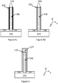
- a Cartesian xyz coordinate system is indicated, which reveals the respective positional relationships of the different components illustrated in the figures.
- the x-, y- and z-axis of this coordinate system meet at a point. Each axis is perpendicular to the other two.
- the x-axis (or x-direction) extends to the right
- the y-axis (or y-direction) extends perpendicular to the drawing plane
- the z-axis (or z-direction) extends upwards.
- 'in contact with' this refers to 'in physical contact with'
- electrical contact with' when an electrical contact is meant, 'in electrical contact with' will be used.
- 'layer A When for example 'layer A is in direct contact with layer B', this means there is a physical contact between layer A and layer B and they are thus formed next to each other having an interface between layer A and layer B.
- 'layer A When for example 'layer A is in electrical contact with layer B' there is not necessarily a '(direct) physical contact' between the two layers, but current should be able to flow from layer A to layer B.
- TFETs Vertical tunneling field effect transistors
- the substrate surface is in the (x,y) plane, whereas the tunnel junction surface is in the (y,z)-plane, the (x,z)-plane or a combination thereof. More specifically described herein are vertical line TFETs.
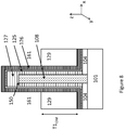
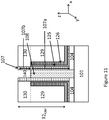
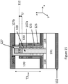
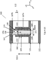
- a vertical tunneling field effect transistor TFET 100 comprising a vertical core region 150 extending perpendicularly from a semiconductor substrate 101, the vertical core region 150 having a top surface 109, the vertical core region 150 consisting of a doped outer part 171 and a middle part 170; a vertical source region 108 comprising the doped outer part 171 of the vertical core region 150; a vertical drain region 107 comprising along its longitudinal direction a first drain part 107a and a second drain part 107b, the first drain part 107a either directly surrounding said vertical source region 108 or directly sandwiching said vertical source region 108 between two sub-parts of said first drain part 107a, the second drain part located directly above and in contact with the first drain part, a gate dielectric layer 105 directly aside of the first drain part 107a of the vertical drain region 107; a gate layer 106 directly aside of the gate dielectric layer 105; the second drain part 107b extending above the height of the gate layer 106 and gate dielectric layer 105; a drain
- An active region 300 (thick dashed rectangle in figures) of the vertical TFET is defined by a the region of height 300H and of width 300W where the tunneling event takes place and is defined by the region comprising part of 107a and part of 108 over a length equal to the maximum vertical distance where part of the vertical source region 108, part of the first part 107a of the vertical drain region 107, part of the gate dielectric layer 105 and part of the gate layer 106 are located next to one another.
- the active region width 300W (horizontal dotted arrow) of the active region 300 is defined by the sum of the width (or thicknesses) of the vertical source region 108 (if present including twice the widths of the transition layer 120 and/or auxiliary source layer 190), twice the width of the first part 107a of the vertical drain region 107.
- Width is in this case the distance of the respective regions/layers in the horizontal direction (x-direction). Width may be also referred to as the thickness of the layer.
- the active region height 300H (vertical dotted arrow) of the active region 300 is equal to the smallest of the height of the first drain part 107a of the vertical drain region 107, which is the distance of the first drain part 107a in the longitudinal direction (z-direction), and the height of the vertical source region 108, which is the distance of the vertical source region 108 in the longitudinal direction (z-direction).
- 300H is equal to the height of the first drain part 107a of the vertical drain region 107 (which is equal to the height of the vertical source region 108).
- there is an underlap U and 300H is equal to the height of the vertical source region 108.
- the vertical source region may comprise only a doped outer part 171 of the vertical core region (as in figure 4b ).
- the active region width 300W may be defined as the thickness of the vertical core region (and if present twice the widths of the transition layer 120 and/or auxiliary source layer 190) and twice the width of the first part 107a of the vertical drain region 107 - although no current will flow through the middle undoped part 170 of the vertical core region.
- a method for manufacturing a vertical TFET (100) comprising the steps of providing a semiconductor substrate (step 201); providing a vertical source region (step 202) extending above the semiconductor substrate; providing a vertical drain region (step 203) comprising along its longitudinal direction a first drain part and above and in contact of the first drain part a second drain part, the first drain part either directly surrounding said vertical source region or directly sandwiching said vertical source region between two sub-parts of said first drain part; providing a gate dielectric layer (step 204) directly aside of the first drain part of the vertical drain region; providing a gate layer (step 205) directly aside of said gate dielectric layer; providing an isolation region between the vertical source region and a drain contact (step 206); providing the drain contact (step 207) to a third drain part, the third drain part being an upper part of the second drain part of the vertical drain region; providing a source contact (step 208) to the vertical source region and providing a gate contact (step 209) to the gate layer.
- FIG. 2 shows the following process steps for a method for forming a vertical tunneling field effect transistor (FET) according to different embodiments of the present invention:
- the vertical TFET device 100 comprises a semiconductor substrate 101.
- a substrate 101 is provided (step 201).
- the substrate 101 is a semiconductor substrate.
- the substrate can for example be a silicon substrate, a substrate of a group IV material, a substrate of a III/V material, a III/V material on Si substrate using strain relaxed buffer layer (SRB) or aspect ratio trapping (ART) or a silicon on insulator (SOI) substrate.
- SRB strain relaxed buffer layer
- ART aspect ratio trapping
- SOI silicon on insulator
- III/V material relates to a material comprising a chemical compound with at least one group III (IUPAC group 13) element and at least one group V element (IUPAC group 15). This includes binary compounds but also higher order compounds such as ternary compounds.
- Providing a semiconductor substrate 101 may comprise providing substrate material and doping the substrate material according to techniques know to a person skilled in the art such as for example ion implantation or diffusion techniques. Doping of the semiconductor substrate may be performed during provision of the substrate material (e.g. by adding appropriate doping gases during growth of the substrate material) or after provision of the substrate material. Doping the substrate material may comprise doping only a top layer of the semiconductor material.
- the semiconductor substrate 101 e.g. silicon substrate, should be doped with the same doping type as the vertical source region 108 of the vertical TFET device. At least a top layer/part of the semiconductor substrate 101 should be highly doped with the same doping type as the vertical source region 108. For example a top layer having a thickness of approximately 50nm with highly doped material should be enough. In an embodiment, a top layer having a thickness of at least 50 nm is highly doped with the same doping type as the vertical source region 108.
- the semiconductor substrate 101 may also be completely highly doped with the same doping type as the vertical source region 108.
- highly doped is meant at least a doping concentration of 1e17 at/cm 3 or higher, preferably 1e19 at/cm3 or higher.
- the doping type of the semiconductor substrate 101 should be the same doping type as the vertical source region 108, since the source contact will be provided to the vertical source region 108 via the doped part of the semiconductor substrate. If the vertical source region 108 comprises a n-doped material, also at least the top layer of the semiconductor substrate should comprise n-doped material.
- the vertical TFET device may further comprise a dielectric isolation layer 104.
- he dielectric isolation layer 104 is provided (step 210 in figure 2 ) on top of a major surface of the substrate 101 ( fig. 3 ).
- the dielectric isolation layer 104 can be made of any suitable material which is selectively removable towards the underlying substrate 101, and towards a hard mask or photoresist to be provided on top thereof for patterning.
- the dielectric material 104 may for example be an oxide layer (SiO 2 ) and may be provided using techniques well known for a person skilled in the art such as for example oxidation or chemical vapor deposition techniques.
- the dielectric isolation layer 104 will serve as an isolation layer between the substrate and subsequent materials/layers being formed above the dielectric layer.
- the thickness of the dielectric layer 104 should be thick enough to electrically isolate the substrate for the subsequent materials/layers (such as for example isolating the substrate from the vertical drain region 107).
- the dielectric isolation layer 104 is patterned thereby exposing part of the underlying semiconductor substrate 101 through an opening 160 ( fig. 3 ). Patterning may be done using lithographic techniques comprising providing a hard mask (not shown) on the dielectric isolation layer and providing a resist layer (not shown) on the hard mask layer, exposing the resist layer by lithography and transferring the exposed resist layer to the underlying hard mask layer. The underlying dielectric isolation layer 104 may thereafter be patterned using the patterned hard mask layer.
- the dielectric isolation layer 104 may be provided between the step of providing a semiconductor substrate and providing a vertical core region 150 (such that the vertical core region 150 (and the vertical source region 108) may be formed selectively in the opening 160) or the dielectric isolation layer 104 may be provided after the step of providing a vertical core region 150.
- the vertical core region 150 when the vertical core region 150 is a nanowire, it can only be grown/formed in the opening 160 on controlled locations if the dielectric isolation layer 104 is deposited and patterned before nanowire growth.
- the vertical TFET device 100 further comprises a vertical core region 150 of a semiconductor core material extending perpendicularly from the semiconductor substrate 101 (through said opening 160), the vertical core region 150 having a top surface 109, the vertical core region 150 comprising at least a doped outer part 171 and a middle part 170, the doped outer part 171 of the vertical core region 150 being (part of) the vertical source region 108 of the TFET device.
- a vertical source region 108 is provided on the semiconductor substrate (step 202). This involves providing a vertical core region 150 and doping at least an outer part 171 of the vertical core region 150. The doped outer part 171 of the vertical core region 150 is then (part of) the vertical source region 108 of the TFET device.
- the vertical source region may further comprise a transition layer 120 or an auxiliary source layer 190.
- the vertical core region 150 is formed vertically extending above the semiconductor substrate 101. With vertically extending is meant that the vertical core region 150 is formed in a vertical direction (z-direction) upward from a horizontal ((x,y)-plane) top surface of the semiconductor substrate 101, thus having a longitudinal axis.
- the vertical core region 150 is preferably an elongated nanostructure and more preferably a nanowire.
- the diameter of the nanowire, perpendicular (x- or y-direction) to its longitudinal axis (z-direction), may be in the range of 1 nm up to 500 nm, for example the diameter of the nanowire may be between 2 and 200 nm.
- the length of the nanowire, along its longitudinal axis (z-direction) may be in the range of 5 nm and 50 ⁇ m, for example the length of the nanowire used in the TFET of the present invention may be between 10 nm and 1 ⁇ m.
- embodiments of the present invention are not limited thereto and implementation by other suitable shapes or geometries is possible.
- a vertically-standing two dimensional layer such as is the case for FINFETs, may be used, or a tubular geometry, that is, a cylindrical or u-shaped structure, for example, carbon nanotubes (CNTs) may be used.
- the vertical core region 150 may be formed with a top-down approach.
- the vertical core region 150 may be formed by first depositing a thick layer of dielectric material (not shown) on the semiconductor substrate, thereafter etching an opening or trench through the dielectric material thereby exposing the underlying semiconductor substrate 101 and subsequently filling the opening or trench with the semiconductor core material. According to embodiments the vertical core region 150 may be formed by first depositing a thick layer of semiconductor core material on the semiconductor substrate, thereafter patterning the layer of semiconductor core material thereby forming the vertical core nanostructure.
- the vertical core region 150 may be formed by a bottom-up approach such as for example Vapor-Liquid-Solid (VLS) synthesis to grow nanowire structures.
- VLS Vapor-Liquid-Solid
- MOCVD metal organic chemical vapor deposition
- the process conditions are such that the growth is preferential in the vertical direction, and suppressed in the lateral direction, in order to obtain a vertical core region 150 with a nanowire shape.
- the vertical growth of the core region can be promoted with the use of a catalyst in combination with metal organic chemical vapor deposition (MOCVD). If this is the case, the catalyst has to be provided in the hole 160, not completely covering the underlying substrate 101 to allow the MOCVD precursors to reach the substrate 101 ( figure 3 ).
- the outer part 171 of the vertical core region 150 is doped thereby forming (part of) the vertical source region 108 of the TFET device 100 ( fig. 4a, 4b ).
- an outer part 171 of the vertical core region 150 is doped such that in this case the vertical source region 108 comprises the outer doped part 171 ( fig. 4b ).
- the complete vertical core region 150 may be doped so that the vertical source region 108 is in this case comprising the entire vertical core region 150 ( fig. 4a ).
- the vertical core region 150 comprises thus semiconductor core material which is completely or partially doped.
- the doped part of semiconductor core material may serve as the source region of the vertical TFET device 100.
- the vertical source region 108 has the same doping type as the semiconductor substrate 101 or as the top layer of the semiconductor substrate 101 (in case only the top layer of the semiconductor substrate is doped).
- the vertical core region 150 then comprises according to these embodiments a middle part 170 which is undoped or intrinsically doped and an outer part, the vertical source region 108, which is doped according to the needs for the source region of the device (see further).
- the doped part of semiconductor material should be preferably at least at the sidewalls of the vertical core region 150 and may also be at the top surface of the vertical core region 150.
- the vertical core region 150 may for example be doped using a tilted implantation technique such that dopants enter the vertical core region 150 at the sidewalls.
- the outer part 171 of the vertical core region 150 is meant about 1 nm up to 20 nm of the outer part of the vertical core region 150 depending on the doping concentration.
- a doping concentration of higher than 1e19/cm 3 a doping spanning of at least a 10 nm thickness of the outer part of the vertical core region 150 may be sufficient.
- a doping concentration from 1e17 to 1e19 e.g. about 1e18/cm 3
- a thicker part of the outer part of the vertical core region 150 may be doped (e.g. at least 20 nm).
- the semiconducting core material for the vertical core region 150 may be selected from at least one group IV materials such as Si, Ge, C and binary compounds thereof, Group III and V materials such as In, Ga, As, Sb, Al, P, B, N and binary, tertiary and quaternary compounds thereof or Group II and VI materials such as Cd, Zn, S, Se, Te, O and binary, tertiary and quaternary compounds thereof, and carbon nanotubes.
- group IV materials such as Si, Ge, C and binary compounds thereof, Group III and V materials such as In, Ga, As, Sb, Al, P, B, N and binary, tertiary and quaternary compounds thereof or Group II and VI materials such as Cd, Zn, S, Se, Te, O and binary, tertiary and quaternary compounds thereof, and carbon nanotubes.
- the vertical source (core) region 108 (or at least the outer part 107 of the vertical core region 150) may be p-doped in case of a n-type TFET (or alternatively in case of a p-type TFET the vertical source region 108 may be n doped).
- the vertical source region 108 (or at least the outer part 171 of the vertical core region 150) is preferably highly doped, i.e. a doping concentration of 1e17 at/cm3 or higher, for example the doping concentration (doping level) of the source region 108 may be in the range of 1e17/cm 3 to 4e21 /cm 3 , for example in the range of 1e19/cm 3 to 5e20/cm 3 .
- n-TFET or p-TFET different dopant types may be used for the vertical source region 108.
- possible p-type dopants are B, Al, Ga, In, TI, Pd, Na, Be, Zn, Au, Co, V, Ni, MO, Hg, Sr, Ge, Cu, K, Sn, W, Pb, O, Fe; and possible n-type dopants are Li, Sb, P, As, Bi, Te, Ti, C, Mg, Se, Cr, Ta, Cs, Ba, S, Mn, Ag, Cd, Pt.
- possible p-type dopants are B, Al, Tl, Ga, In, Be, Zn, Cr, Cd, Hg, Co, Ni, Mn, Fe, Pt; and possible n-type dopants are Li, Sb, P, As, S, Se, Te, Cu, Au, Ag.
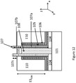
- the vertical source layer may further comprise a transition layer 120 or an auxiliary source layer 190 which is formed aside of the doped outer part 171 of the vertical core region 150 (step 211 in figure 2 ).
- the vertical source region 108 may thus comprise a transition layer 120.
- the transition layer 120 is formed aside of the vertical core region 150 ( fig. 4c ).
- the vertical source region 108 of the TFET device thus consists then of the doped (outer part or complete) vertical core region of a semiconductor core material and the transition layer 120.
- the transition layer 120 comprises preferably a semiconductor different from the semiconductor core material (e.g.
- the transition layer 120 may also comprise an insulating material like an oxide, nitride, .... in which case the layer would help to stop the tunneling current when the gate voltage brings the device in its off-state.
- the transition layer 120 is preferably a few monolayers. The thickness of the transition layer 120 may be from one monolayer up to about 2 nm.
- the vertical source region 108 may further comprise an auxiliary source layer 190.
- the auxiliary source layer 190 is formed aside of the vertical core region 150 ( fig. 4d ).
- the vertical source region of the TFET 108 device thus consists then of the doped (outer part or complete) vertical core region 150 of a semiconductor core material and the auxiliary source layer 190 of another semiconductor material.
- the semiconductor core material is then preferably a material which is easily grown from the substrate.
- the thickness of the auxiliary source layer 190 is depending on the doping concentration of source layer 190.
- the thickness of the auxiliary source layer 190 should be sufficient such that the active region (see further) of the TFET device does not reach into the doped semiconductor core material of the vertical core region.
- the auxiliary source layer 190 acts in this case as a kind of 'effective source' of the TFET device as the tunneling paths will only be present in this part (i.e. the auxiliary source layer) of the vertical source region 108 and not in the doped part of the vertical core region.
- auxiliary source layer 190 may be formed of a material which has a better alignment of the band structure towards the vertical drain region.
- a first (vertical core semiconductor) material is used which may be grown easily on the substrate and thereafter the second other material (the auxiliary source layer) is used as to optimize the tunneling properties of the device.
- auxiliary source layer 190 that a heterojunction may be formed between the auxiliary source layer and the vertical drain region with high tunnel efficiency, while retaining a vertical core region of another material which can easily be grown epitaxial in a nanowire configuration.
- the main difference between the transition layer 120 and the auxiliary source layer 190 are their thickness and their function.
- the transition layer 120 only needs a few monolayers whereas the auxiliary source layer 190 should have a thickness of at least several nm's.
- the transition layer 120 is to promote a better epitaxial growth or (if insulating material) to decrease the off-current, whereas the auxiliary source layer 190 is to get a better tunneling event towards the vertical drain region, this is to enhance the device's on-current.
- the TFET device 100 further comprises a vertical drain region 107 comprising along its longitudinal direction a first drain part 107a and a second drain part 107b, the first drain part 107a either directly surrounding said vertical source region (108) or directly sandwiching said vertical source region 108 between two sub-parts of said first drain part 107a.
- the vertical core region is a nanowire
- the vertical drain region 107 is located (substantially circumferentially) around the nanowire.
- the vertical drain region 107 comprises a semiconducting drain material.
- the semiconductor drain material is preferably different form the semiconducting source material (i.e. heterostructure).
- the different materials for the vertical source region and the vertical drain region are necessary to enable a selective etch of the source region towards the drain region in the manufacturing method of the device.
- the heterostructure is not necessary and one may use identical materials (homostructure) for both the semiconducting core material and the semiconducting drain material.
- the semiconducting drain material for the vertical drain region 107 may be selected from group IV materials such as Si, Ge, C and binary compounds thereof, Group III and V materials such as In, Ga, As, Sb, Al, P, B, N and binary, tertiary and quaternary compounds thereof, and Group II and VI materials such as Cd, Zn, S, Se, Te, O and binary, tertiary and quaternary compounds thereof.
- group IV materials such as Si, Ge, C and binary compounds thereof
- Group III and V materials such as In, Ga, As, Sb, Al, P, B, N and binary, tertiary and quaternary compounds thereof
- Group II and VI materials such as Cd, Zn, S, Se, Te, O and binary, tertiary and quaternary compounds thereof.
- the vertical drain region 107 may be undoped or intrinsically doped, highly doped or lowly doped.
- the vertical drain region 107 may be lowly doped, i.e. a do
- the vertical drain region 107 has - in case of highly doped - a doping type which is opposite to the doping type of the vertical source region 108.
- the vertical drain region 107 has - in case of lowly or intrinsically doped - a doping type which is the same or opposite to the doping type of the vertical source region 108.
- the vertical drain region 107 comprises a first drain part 107a and a second drain part 107b.
- the first drain part 107a is in direct electrical and physical contact with the vertical source region 108 (i.e. the doped part of the vertical core region and optionally the transition layer or auxiliary source layer) on one side and with the gate dielectric layer 105 on the other side.
- the second drain part 107b is located in direct contact and above the first drain part 107a.
- the second drain part 107b may be in contact with the vertical source region 108.
- the second drain part 107b is not in contact with the gate dielectric layer 105.
- the second drain part 107b is thus the part of the vertical drain region 107 which is extending above the gate dielectric layer 105, shown by the dashed line 112.
- the second drain part 107b is not in direct physical contact with the vertical source region 108 on the one side nor with the gate dielectric layer 105 on the other side ( fig. 1 ).
- the vertical source region 108 is thus sandwiched in between or surrounded by (depending on the geometry) the first drain part 107a, and not in between or surrounded by the second drain part 107b.
- the second drain part 107b is thus extending above the height of the vertical source region 108.
- the second drain part 107b may be partially in direct physical contact with the vertical source region 108 on one side, but is not in direct physical contact with the gate dielectric layer 105 on the other side ( figure 17 ).
- At least part of or the complete second drain part 107b is extending above the height of the vertical source region 108 in order to establish a contact between the vertical drain region 107 via the second drain part 107b and a drain contact 103.
- the vertical drain region 107 more specifically the second drain part 107b, further comprises a third drain part 107c which is in direct physical contact with the drain contact 103 (see further).
- the third drain part 107c is thus an upper part of the second drain part 107b.
- the non-overlapping remaining (lower) part of the second drain part 107b is not in direct physical contact with the drain contact.
- the vertical drain region may have a thickness of from 1 monolayer to 20 nm, more preferably 1nm to 10 nm. With thickness is meant the extent of the layer in the horizontal direction (x-direction).
- the height in the longitudinal or vertical direction (z-direction) of the vertical drain region is larger than the height in the longitudinal or vertical direction (z-direction) of the vertical source region 108, of the gate dielectric layer 105 and of the gate layer 106.
- the vertical source region 108 (if present including the transition layer 120 or auxiliary source layer 190) and the vertical drain region 107 of the vertical TFET are in direct contact with each other along at least part of 107, no explicit so-called intrinsic channel region is present in the vertical TFET device according to the present invention as compared to the known p-i-n vertical TFET devices such as for example described in US patent application US2011/0253981 A1 . Otherwise said there is no intrinsic (third) region between the source region 108 and the drain region 107.
- the buffer layer 132 which may be an intrinsic semiconductor with large band gap, is not to be seen as an intrinsic channel region, because the desired device current does not flow through this buffer layer 132, only leakage currents may flow through the buffer layer 132.
- the desired device current flows from the source contact 102 through the doped region in the substrate 101 to the vertical source region 108 (being only a doped outer layer or the complete vertical core region), if present through a transition layer 120 and/or auxiliary source layer 190 to the vertical drain layer 107 and then upward along 107 to the drain contact 103. In this path of the desired tunnel current, there is no so-called intrinsic channel region (third region) between the source and the drain which needs to be crossed.
- the semiconducting core material 108 and the semiconducting drain material 107 may be the same material, as such being a homostructure and not a heterostructure as generally stated.
- a key aspect of the present invention is thus that there is no parasitic path from source to drain, this is a path where the gate has no gate control, because above region 108 there is region 131 (comprising insulating material). This is possible due to the selective removal of material 108 with respect to material 107.
- the only path for current is the path which runs through the active region and which comprises the tunnel junction.
- p-i-n TFETs an i-channel region is needed, because the gate typically cannot control the full body thickness of the TFET efficiently and hence a p-n diode with a gate would have a very large leakage current as the gate cannot turn off the tunneling in the center of the device.
- the active region 300 (thick dotted rectangle in figures) of the vertical TFET is thus defined by the region of height 300H and width 300W where the vertical source region 108, the first part 107a of the vertical drain region 107, the gate dielectric layer 105 and the gate layer 106 are located next to one another.
- the active region comprises part of the vertical source region (including if present part of the transition layer and/or auxiliary source layer), part of the vertical drain region.
- the vertical drain region 107 is provided (step 203) - after the step of forming the vertical source region 108 - aside of the vertical source region 108 (step 203).
- a transition layer 120 or auxiliary source layer 190 may be present between the vertical source region 108 and the vertical drain region 107 (or more specifically the first part of the vertical drain region 107a) ( figure 17 ).
- the transition layer 120 or the auxiliary source layer 190 is regarded to be part of the source of the TFET device.
- the source of the TFET is defined by the vertical source region 108, the transition layer 120 and/or the auxiliary source layer 190.
- the embodiments of the method for forming a TFET device ( figures 5-14 ) and the example not covered by the claim ( figure 15 ) will now be further described with reference to a vertical core region 150 which is completely doped thereby forming the vertical source region 108.
- the steps may be adapted towards the different embodiments for a vertical source region 108 as described above.
- providing the vertical drain region 107 comprises depositing a layer of semiconducting drain material 127 on the vertical source region 108 ( figure 5 ).
- the layer of semiconducting drain material 127 is provided using well known deposition techniques such as metal organic chemical vapor deposition (MOCVD) in such a way that the material is grown selectively on the vertical source region 108, which means sideways growth from the vertical surface and vertical growth from the top surface.
- MOCVD metal organic chemical vapor deposition
- the layer of semiconducting drain material 127 is thus present at the sidewalls of the vertical core region 108 and on top of the vertical core region 108.
- the layer of semiconducting drain material 127 is (electrically) isolated from the substrate by the dielectric isolation layer 104.
- the semiconducting drain material 127 is provided immediately after providing the vertical source region 108 without intermediate processing steps or air breaks, in order to provide an interface with a minimal amount of defects and impurities.
- a layer of gate dielectric material 125 may be provided on the layer of semiconducting drain material 127 ( figure 6 ).
- a layer of gate material 126 may be provided on the layer of gate dielectric material 125 ( figure 6 ).
- Both layers 125, 126 may be deposited in-situ for example using well known deposition techniques such as atomic layer deposition (ALD).
- the gate material may also be obtained by well-known techniques such as sputtering or evaporation.
- a conformal deposition of the layers 125 and 126 is obtained around the semiconducting drain material 127 also preferably immediately after the provision of the semiconducting drain material 127.
- the gate length of the vertical TFET device cannot be defined as the gate length in prior art planar TFET or finfet-based configuration.
- Gate length of the vertical TFET according to the present invention may be defined as the active region height 300H over which the vertical source region, if present the transition layer and/or auxiliary source layer, the vertical drain region and the gate region overlap.
- the gate length of the vertical TFET device is thus defined by the region where the tunneling takes place. Due to the vertical direction of the tunnel junction surface (being perpendicular to the substrate surface), the on-current of the vertical TFET device will scale with the gate length.
- the layer of gate dielectric material 125 and the layer of gate material 126 may be patterned for separating the different gate stacks from one another (not illustrated in the drawings). This patterning may be performed by means of a resist masked dry etch of the different layers 125, 126 in an isotropic way. In particular embodiments, the patterning is such that gate stacks of nanowires are not electrically connected to each other. This patterning is such that the gate layer 106 does not extend beyond the gate dielectric layer 105, hence is not in direct contact with the dielectric isolation layer 104. Patterning of the gate stack for separation of the gates does not need to be performed immediately after the gate stack deposition; it can also be done later.
- an interlayer dielectric material 129 is provided over the gate structure ( figure 7 ).
- This interlayer dielectric material 129 may for example be an oxide layer, e.g. a High Density Plasma (HDP) oxide.
- the interlayer dielectric material 129 may be different from the material of the dielectric insulation layer 104.
- the provided interlayer dielectric material 129 is planarised, for example by a mechanical planarization method such as e.g. Chemical Mechanical Planarization (CMP), followed by an etch back step for removing part of interlayer dielectric material 129 around the vertical source region 108, so as to reveal the gate electrode material 126 as illustrated in figure 8 .
- the thickness T1 IDM of the remaining interlayer dielectric material 129 must be equal or lower than the height of the vertical source region 108 (except for the embodiments relating to figure 15 ).
- the uncovered layer of gate dielectric material 125 and layer of gate material 126 are selectively removed with a dry etch step. This is illustrated in figure 9 .
- the removal of the layer of gate dielectric material 125 and layer of gate material 126 comprises subsequent removal steps of the revealed part of the layer of gate material 126 and of the revealed part of the layer of gate dielectric material 125.
- part of the layer of semiconducting drain material 127 is revealed. Etching of the layer of gate material 126 and the layer of gate dielectric material 125 should thus be selective towards the semiconducting drain material 127.
- part of the open regions 161 next to the semiconducting drain material 127 is refilled again with interlayer dielectric material 130 thereby increasing the thickness T1 IDM to another thickness T2 IDM ( figure 10 ).
- the interlayer dielectric material 130 is preferably the same as the interlayer dielectric material 129.
- the thickness T2 IDM must be sufficient to guarantee that no electrical contact is possible between the final gate structure 105, 106 and the final drain contact 103.
- the maximal thickness T2 IDM is equal to the final height of the vertical drain region 107.
- the minimal thickness T2 IDM is such that there is no electrical contact between 103 and 105 after the next step being recessing the inter dielectric material 130 again to another thickness T3 IDM .
- T1 IDM is smaller than T3 IDM and T3 IDM is smaller than T2 IDM .
- part of the semiconducting drain material 127 remains exposed and is extending above the level of the top surface of the interlayer dielectric material 130. Also the vertical source region 108 may - at this point in the process flow - extend above the level of the interlayer dielectric material 130 ( figure 10 ).
- part of the vertical source material 108 is removed, thereby leaving a cavity 140 in between the walls of the second vertical drain part, more specifically a cavity 140 between the walls of the second drain parts 107b.
- Removing part of the semiconducting drain material 127 and removing part of the vertical source region 108 may be done using etching steps known for a person skilled in the art. It is advantageous to choose the semiconducting drain material and the semiconducting core material so that they may be etched selectively. For example a dry etching step may be used to remove the semiconducting drain material 127, without affecting the semiconducting core (source) material.
- a selective wet etching step may be used to remove the semiconducting core material, without affecting the remaining semiconducting drain material 127.
- Other examples of methods for selectively removing the drain material 127 and source material include reactive ion etching (RIE) or inductively coupled plasma (ICP) etching.
- first drain part 107a and a second drain part 107b may be defined.
- the first drain part 107a is in direct electrical and physical contact with the vertical source region 108 on one side and with the gate dielectric layer (105) on the other side.
- the second drain part 107b is not in direct physical contact with the vertical source region 108 on the one side nor with the gate dielectric layer 105 on the other side ( fig. 1 ).
- the second drain part 107b is not in direct physical contact with the vertical source region 108 on one side, and thus is extending upwards above the level of a top surface 109 of the vertical source region 108, but may be partially in direct physical contact with the gate dielectric layer 105 on the other side ( figure 16 ). According to embodiments the second drain part 107b is partially in direct physical contact with the vertical source region 108 on one side, but is not in direct physical contact with the gate dielectric layer 105 on the other side ( figure 17 ). At least part of or the complete second drain part 107b is thus extending above the level of the vertical source region 108 in order to contact the vertical drain region 107 via the second drain part 107b to a drain contact 103.
- the cavity 140 above the vertical source region 108 is refilled ( figure 12 ). This may be done according to different embodiments.
- the cavity 140 may be refilled with dielectric material 131 and thereafter top part of the dielectric material 130, 131 may be removed thereby leaving a third drain part 107c of the second drain part 107b exposed ( figure 12 ). After removing part of the dielectric material 130 the final dielectric region is now referred to as region 110 at both sides of the vertical TFET device.
- the TFET comprises a gate structure 105, 106, the gate structure 105, 106 comprising a gate dielectric layer 105 in contact with the first drain part 107a of the vertical drain region 107 and a gate layer 106 in contact with the gate dielectric layer 105.
- the dielectric material for the gate dielectric layer 105 may be selected from silicon based oxides (e.g.
- the gate dielectric layer may comprise hafnium oxide.
- the conductive material for the gate layer 106 may be selected from polysilicon, polygermanium, metals such as Al, W, Ta, Ti, Ru, Pd, Rh, Re, PT and alloys thereof, metal nitrides such as TaN, TiN, metal silicon nitrides such as TaSiN, conductive oxides such as RuO 2 and ReO 3 , fully silicided metals (FUSI) such as CoSi, NiSi, TiSi 2 , fully germanided metals (FUGE), work function tunable metals, and materials engineered to obtain a particular gate work function. More particularly the gate layer may be made of a metal of which the work function has been engineered specifically for the chosen TFET semiconductor material.
- the gate structure i.e. the gate dielectric layer 105 and the gate layer 106, is provided (step 204, 205) after the step of providing the vertical drain region.
- the top surface 109 of the vertical source region 108 may be higher than, lower than or equal to the height 112 to which the gate structure 105, 106 is extending along the sidewall of the vertical source region 108.
- the vertical source region 108 may thus extend above the level of the gate, below the level of the gate or may be aligned with the level the gate.
- the top surface of the vertical source region 108 is aligned to the height 112 to which the gate structure 105, 106 is extending along the sidewall of the vertical source region 108.
- 15 and 16 for example the top surface of the vertical source region 108 is lower than the height 112 to which the gate structure 105, 106 is extending along the sidewall of the vertical source region 108.
- the underlap U is the difference in height between the top surface of the vertical source region 108 and the top 112 of the gate structure 105, 106.
- the top surface of the vertical source region 108 is higher than the height 112 to which the gate structure 105, 106 is extending along the sidewall of the vertical source region 108.
- the overlap O is the difference in height between the top surface of the vertical source region 108 and the top 112 of the gate structure 105, 106.
- Each of the vertical source region 108, vertical drain region 107 and vertical gate structure are in electrical contact with respectively a source contact 102, a drain contact 103 and a gate contact.
- Source contact 102, drain contact 103 and gate contact are electrically isolated from each other.
- the placement of the source contact 102, drain contact 103 and gate contact is rather illustrative in the figures. In the example described the source contact 102 is placed at the backside of the substrate. It should be noted this is only one example and a person skilled in the art will be able to have other examples for placing the source contact 102, such as for example the source contact could also be present aside of the vertical TFET (not shown).
- the source contact 102 must be electrically connected to the vertical source region 108.
- the contact may be a direct physical contact or an indirect contact such as for example shown in figure 1 , where the source contact 102 is at the backside of the semiconductor substrate 101 and the vertical source region 108 is thus electrically contacted to the source contact 102 via the semiconductor substrate 101.
- the source contact 102 may for example also be located aside of the TFET device and electrically contacted to the source contact 102 via the semiconductor substrate 101 (not shown).
- the drain contact 103 must be connected to the vertical drain region 107 and even more specifically to third drain part 107c of the second drain part 107b.
- the gate contact must be connected to the gate layer 106.
- the drain contact 103 is not in contact with the first drain part 107a of the vertical drain region 107 as this would lead to a shortening with the source region 108 and/or gate structure 105, 106.
- the gate contact is not shown in the figures but may for example be formed by etching a via through the interlayer dielectric 110 and thereby connecting to the gate layer 106.
- the source contact, drain contact and gate contact region may be made from a conductive material which is selected from silicide containing structures (NiSi, CoSi 2 , TiSi 2 ,...), germanide containing structures, metal containing structures, polysilicon or a combination thereof. More particularly the contact may be a combination of a metal with a silicide.
- drain contact 103 source contact 102 and gate contact should be isolated from each other.
- the vertical source region 108 and the drain contact 103 should be isolated from each other. This is done by an insulating material 131 formed in the cavity 140 in between the vertical source region 108 and the drain contact 103.
- a buffer region 132 may be formed in the cavity 140 above the vertical source region 108 ( figure 14 ). Instead of having a separation between the vertical source region 108 and the vertical drain region 107b by the insulating dielectric material 131, the separation/insulation is done using the buffer region 132 together with the insulating dielectric material 131.
- the buffer region 132 may comprise a semiconductor material which may be epitaxial grown on top of the vertical source region 108.
- the buffer region 132 preferably comprises an intrinsic semiconductor material such as for example group IV materials such as Si, Ge, C and binary compounds thereof, or Group III-V materials such as In, Ga, As, Sb, Al, P, B, N and binary, tertiary and quaternary compounds thereof or Group II-VI materials such as Cd, Zn, S, Se, Te, O and binary, tertiary and quaternary compounds thereof, or preferentially a semiconductor material with a large band gap such that no parasitic currents are running from 108 through 132 to 103, such as for example GaP, AlAs, GaAs, InAIAs, InP, or AlSb.
- an AlSb buffer layer 132 may be grown on top of an InAs nanowire (source) 108 and with an GaAsSb shell layer (drain) 127 formed around the AlSb buffer layer 132 and the InAs nanowire.
- the advantage of using a buffer layer 132 on top of the vertical source region 108 is that the vertical source region 108 is protected from further etching steps (such as for example etching of the vertical drain region 107) thus lowering the amount of defects at the tunnel junction and thus lowering the amount of leakage current.
- Another advantage of using a buffer layer 132 on top of the vertical source region 108 is that there is no specific need to etch the vertical drain region 107 (see figure 15 ).
- Figure 15 shows a schematic representation of a vertical TFET device according to an example not covered by the claims wherein the buffer layer 132 is formed on the vertical source region 108 before the step of providing a vertical drain material 127.
- the vertical drain material 127 is thereafter not removed and remains over the vertical source region 108 and the buffer layer 132 as shown in figure 15 .
- the third drain part 107c is present on top of the buffer layer 132.
- the vertical source region 108 there may be an overlap O of the vertical source region 108 with respect to the gate structure 125, 126 (see for example figure 17 , 18 ).
- the vertical source region may have a height higher than the gate structure 125, 126.
- the overlap has the advantage that there is a lower gate control over the defective top of the vertical source region 108, hence reducing the amount of trap assisted tunneling in this defective region.
Priority Applications (3)
| Application Number | Priority Date | Filing Date | Title |
|---|---|---|---|
| EP13169921.7A EP2808897B1 (en) | 2013-05-30 | 2013-05-30 | Tunnel field effect transistor and method for making thereof |
| US14/289,534 US9318583B2 (en) | 2013-05-30 | 2014-05-28 | Tunnel field effect transistor and method for making thereof |
| KR1020140066268A KR20140141522A (ko) | 2013-05-30 | 2014-05-30 | 터널링 전계 효과 트랜지스터 및 그 제조방법 |
Applications Claiming Priority (1)
| Application Number | Priority Date | Filing Date | Title |
|---|---|---|---|
| EP13169921.7A EP2808897B1 (en) | 2013-05-30 | 2013-05-30 | Tunnel field effect transistor and method for making thereof |
Publications (2)
| Publication Number | Publication Date |
|---|---|
| EP2808897A1 EP2808897A1 (en) | 2014-12-03 |
| EP2808897B1 true EP2808897B1 (en) | 2021-06-30 |
Family
ID=48485078
Family Applications (1)
| Application Number | Title | Priority Date | Filing Date |
|---|---|---|---|
| EP13169921.7A Active EP2808897B1 (en) | 2013-05-30 | 2013-05-30 | Tunnel field effect transistor and method for making thereof |
Country Status (3)
| Country | Link |
|---|---|
| US (1) | US9318583B2 (ko) |
| EP (1) | EP2808897B1 (ko) |
| KR (1) | KR20140141522A (ko) |
Families Citing this family (43)
| Publication number | Priority date | Publication date | Assignee | Title |
|---|---|---|---|---|
| US8916927B2 (en) * | 2012-07-19 | 2014-12-23 | Taiwan Semiconductor Manufacturing | Vertical tunnel field effect transistor (FET) |
| US9614049B2 (en) * | 2013-06-20 | 2017-04-04 | Taiwan Semiconductor Manufacturing Company Limited | Fin tunnel field effect transistor (FET) |
| US20150214114A1 (en) * | 2014-01-28 | 2015-07-30 | United Microelectronics Corp. | Manufacturing method of semiconductor structure |
| CN104617138B (zh) * | 2015-01-26 | 2017-12-08 | 华为技术有限公司 | 隧穿场效应晶体管及其制备方法 |
| US9385195B1 (en) * | 2015-03-31 | 2016-07-05 | Stmicroelectronics, Inc. | Vertical gate-all-around TFET |
| SE1530097A1 (en) * | 2015-06-22 | 2016-12-23 | Method for Vertical Gate-Last Process | |
| WO2017079979A1 (zh) * | 2015-11-13 | 2017-05-18 | 华为技术有限公司 | 一种隧穿场效应晶体管及其制作方法 |
| US9711607B1 (en) * | 2016-04-15 | 2017-07-18 | Taiwan Semiconductor Manufacturing Co., Ltd. | One-dimensional nanostructure growth on graphene and devices thereof |
| US9799751B1 (en) * | 2016-04-19 | 2017-10-24 | Globalfoundries Inc. | Methods of forming a gate structure on a vertical transistor device |
| KR102422240B1 (ko) | 2016-05-26 | 2022-07-18 | 삼성전자주식회사 | 집적회로 소자 및 그 제조 방법 |
| US9735253B1 (en) * | 2016-08-26 | 2017-08-15 | International Business Machines Corporation | Closely packed vertical transistors with reduced contact resistance |
| US10170616B2 (en) | 2016-09-19 | 2019-01-01 | Globalfoundries Inc. | Methods of forming a vertical transistor device |
| US9876088B1 (en) * | 2016-09-19 | 2018-01-23 | Taiwan Semiconductor Manufacturing Co., Ltd. | III-V semiconductor layers, III-V semiconductor devices and methods of manufacturing thereof |
| US10347745B2 (en) | 2016-09-19 | 2019-07-09 | Globalfoundries Inc. | Methods of forming bottom and top source/drain regions on a vertical transistor device |
| US10475673B2 (en) * | 2016-09-28 | 2019-11-12 | Stmicroelectronics S.R.L. | Apparatus for manufacturing a silicon carbide wafer |
| US9882025B1 (en) | 2016-09-30 | 2018-01-30 | Globalfoundries Inc. | Methods of simultaneously forming bottom and top spacers on a vertical transistor device |
| US9966456B1 (en) * | 2016-11-08 | 2018-05-08 | Globalfoundries Inc. | Methods of forming gate electrodes on a vertical transistor device |
| US10608085B2 (en) | 2016-12-23 | 2020-03-31 | Imec Vzw | Two dimensional field effect transistors |
| US9935018B1 (en) | 2017-02-17 | 2018-04-03 | Globalfoundries Inc. | Methods of forming vertical transistor devices with different effective gate lengths |
| US10229999B2 (en) | 2017-02-28 | 2019-03-12 | Globalfoundries Inc. | Methods of forming upper source/drain regions on a vertical transistor device |
| US10014370B1 (en) | 2017-04-19 | 2018-07-03 | Globalfoundries Inc. | Air gap adjacent a bottom source/drain region of vertical transistor device |
| US10957696B2 (en) | 2017-05-12 | 2021-03-23 | International Business Machines Corporation | Self-aligned metal gate with poly silicide for vertical transport field-effect transistors |
| US11018255B2 (en) * | 2017-08-29 | 2021-05-25 | Micron Technology, Inc. | Devices and systems with string drivers including high band gap material and methods of formation |
| US10516039B2 (en) | 2017-11-30 | 2019-12-24 | Taiwan Semiconductor Manufacturing Co., Ltd. | Semiconductor device and manufacturing method thereof |
| US10147808B1 (en) * | 2017-12-04 | 2018-12-04 | International Business Machines Corporation | Techniques for forming vertical tunneling FETS |
| US10355046B1 (en) * | 2017-12-29 | 2019-07-16 | Spin Memory, Inc. | Steep slope field-effect transistor (FET) for a perpendicular magnetic tunnel junction (PMTJ) |
| JP7027949B2 (ja) * | 2018-02-23 | 2022-03-02 | 富士通株式会社 | 半導体装置、受信機及び半導体装置の製造方法 |
| US10424653B1 (en) | 2018-05-21 | 2019-09-24 | International Business Machines Corporation | Vertical transport field effect transistor on silicon with defined junctions |
| US10644150B2 (en) | 2018-06-04 | 2020-05-05 | International Business Machines Corporation | Tunnel field-effect transistor with reduced subthreshold swing |
| US10566251B2 (en) | 2018-07-17 | 2020-02-18 | International Business Machines Corporation | Techniques for forming vertical transport FET |
| CN110942993B (zh) * | 2018-09-25 | 2023-07-21 | 中芯国际集成电路制造(天津)有限公司 | 垂直式环绕栅极场效应晶体管的制备方法 |
| US11309177B2 (en) | 2018-11-06 | 2022-04-19 | Stmicroelectronics S.R.L. | Apparatus and method for manufacturing a wafer |
| CN110061060B (zh) * | 2019-01-25 | 2022-06-24 | 中国科学院微电子研究所 | 半导体器件和制作方法 |
| CN110085672A (zh) * | 2019-04-19 | 2019-08-02 | 宁波大学 | 一种tfet器件 |
| IT201900015416A1 (it) | 2019-09-03 | 2021-03-03 | St Microelectronics Srl | Apparecchio per la crescita di una fetta di materiale semiconduttore, in particolare di carburo di silicio, e procedimento di fabbricazione associato |
| CN112713088B (zh) * | 2019-10-24 | 2023-06-06 | 中芯国际集成电路制造(上海)有限公司 | 半导体结构及其形成方法 |
| KR102292334B1 (ko) * | 2019-12-20 | 2021-08-24 | 서울대학교산학협력단 | 높은 동작전류를 보이는 나노선 tfet의 제조 방법 및 그 나노선 tfet |
| CN111446288B (zh) * | 2020-03-08 | 2021-09-17 | 复旦大学 | 基于二维材料的ns叠层晶体管及其制备方法 |
| US11769831B2 (en) * | 2020-09-30 | 2023-09-26 | Tokyo Electron Limited | High performance floating body VFET with dielectric core |
| CN112397581B (zh) * | 2020-11-18 | 2022-06-10 | 光华临港工程应用技术研发(上海)有限公司 | 隧道场效应晶体管及其制作方法 |
| US11640987B2 (en) * | 2021-02-04 | 2023-05-02 | Applied Materials, Inc. | Implant to form vertical FETs with self-aligned drain spacer and junction |
| CN113571589B (zh) * | 2021-07-26 | 2022-06-03 | 西安电子科技大学 | 异质栅介质的异质结隧穿场效应晶体管及其制作方法 |
| WO2023182099A1 (ja) * | 2022-03-24 | 2023-09-28 | 国立大学法人北海道大学 | 電界効果トランジスタおよびスイッチ素子 |
Family Cites Families (8)
| Publication number | Priority date | Publication date | Assignee | Title |
|---|---|---|---|---|
| JP2773487B2 (ja) | 1991-10-15 | 1998-07-09 | 日本電気株式会社 | トンネルトランジスタ |
| US7893476B2 (en) * | 2006-09-15 | 2011-02-22 | Imec | Tunnel effect transistors based on silicon nanowires |
| KR101663200B1 (ko) | 2009-09-30 | 2016-10-06 | 국립대학법인 홋가이도 다이가쿠 | 터널 전계 효과 트랜지스터 및 그 제조 방법 |
| EP2378557B1 (en) | 2010-04-19 | 2015-12-23 | Imec | Method of manufacturing a vertical TFET |
| US8796733B2 (en) | 2010-08-09 | 2014-08-05 | University Of Notre Dame Du Lac | Low voltage tunnel field-effect transistor (TFET) and method of making same |
| WO2012152762A1 (en) | 2011-05-06 | 2012-11-15 | Imec | Tunnel field effect transistor device |
| US8916927B2 (en) * | 2012-07-19 | 2014-12-23 | Taiwan Semiconductor Manufacturing | Vertical tunnel field effect transistor (FET) |
| US9711632B2 (en) * | 2013-03-13 | 2017-07-18 | Taiwan Semiconductor Manufacturing Co., Ltd. | Intra-band tunnel FET |
-
2013
- 2013-05-30 EP EP13169921.7A patent/EP2808897B1/en active Active
-
2014
- 2014-05-28 US US14/289,534 patent/US9318583B2/en active Active
- 2014-05-30 KR KR1020140066268A patent/KR20140141522A/ko not_active Application Discontinuation
Non-Patent Citations (1)
| Title |
|---|
| None * |
Also Published As
| Publication number | Publication date |
|---|---|
| US20140353593A1 (en) | 2014-12-04 |
| EP2808897A1 (en) | 2014-12-03 |
| KR20140141522A (ko) | 2014-12-10 |
| US9318583B2 (en) | 2016-04-19 |
Similar Documents
| Publication | Publication Date | Title |
|---|---|---|
| EP2808897B1 (en) | Tunnel field effect transistor and method for making thereof | |
| CN107887441B (zh) | 半导体器件及其制造方法及包括该器件的电子设备 | |
| EP1900681B1 (en) | Tunnel Field-Effect Transistors based on silicon nanowires | |
| US8629428B2 (en) | Line-tunneling tunnel field-effect transistor (TFET) and manufacturing method | |
| US8404545B2 (en) | Tunnel field-effect transistor with gated tunnel barrier | |
| KR101401274B1 (ko) | Ge 및/또는 III-V족 화합물 반도체를 이용한 FinFET 및 그 제조방법 | |
| JP5171161B2 (ja) | ナノワイヤトンネル電界効果トランジスタ半導体装置およびその製造方法 | |
| US10896974B2 (en) | Method of fabricating semiconductor device | |
| EP1901354A1 (en) | A tunnel field-effect transistor with gated tunnel barrier | |
| US9960233B2 (en) | Expitaxially regrown heterostructure nanowire lateral tunnel field effect transistor | |
| WO2012085715A1 (en) | Nanowire field -effect device with multiple gates | |
| US11349022B2 (en) | Tunnel field-effect transistor with reduced trap-assisted tunneling leakage | |
| US11557652B2 (en) | Metal source/drain-based MOSFET and method for fabricating the same | |
| CN107039514A (zh) | Iii‑v族纳米线隧穿fet的方法及结构 | |
| CN110957363A (zh) | 半导体装置 | |
| EP1901355B1 (en) | Tunnel effect transistors based on monocrystalline nanowires having a heterostructure | |
| CN210516733U (zh) | 竖直型半导体器件 | |
| WO2018059109A1 (zh) | 半导体器件及其制造方法及包括该器件的电子设备 | |
| US11621340B2 (en) | Field-effect transistor structure and fabrication method |
Legal Events
| Date | Code | Title | Description |
|---|---|---|---|
| PUAI | Public reference made under article 153(3) epc to a published international application that has entered the european phase |
Free format text: ORIGINAL CODE: 0009012 |
|
| 17P | Request for examination filed |
Effective date: 20130530 |
|
| AK | Designated contracting states |
Kind code of ref document: A1 Designated state(s): AL AT BE BG CH CY CZ DE DK EE ES FI FR GB GR HR HU IE IS IT LI LT LU LV MC MK MT NL NO PL PT RO RS SE SI SK SM TR |
|
| AX | Request for extension of the european patent |
Extension state: BA ME |
|
| RIN1 | Information on inventor provided before grant (corrected) |
Inventor name: SMETS, QUENTIN Inventor name: VERHULST, ANNE |
|
| R17P | Request for examination filed (corrected) |
Effective date: 20150602 |
|
| RBV | Designated contracting states (corrected) |
Designated state(s): AL AT BE BG CH CY CZ DE DK EE ES FI FR GB GR HR HU IE IS IT LI LT LU LV MC MK MT NL NO PL PT RO RS SE SI SK SM TR |
|
| RIN1 | Information on inventor provided before grant (corrected) |
Inventor name: SMETS, QUENTIN Inventor name: VERHULST, ANNE |
|
| STAA | Information on the status of an ep patent application or granted ep patent |
Free format text: STATUS: EXAMINATION IS IN PROGRESS |
|
| 17Q | First examination report despatched |
Effective date: 20170801 |
|
| GRAP | Despatch of communication of intention to grant a patent |
Free format text: ORIGINAL CODE: EPIDOSNIGR1 |
|
| STAA | Information on the status of an ep patent application or granted ep patent |
Free format text: STATUS: GRANT OF PATENT IS INTENDED |
|
| RIC1 | Information provided on ipc code assigned before grant |
Ipc: H01L 29/205 20060101ALN20201103BHEP Ipc: H01L 21/33 20060101ALI20201103BHEP Ipc: H01L 29/06 20060101ALI20201103BHEP Ipc: H01L 29/739 20060101AFI20201103BHEP Ipc: H01L 29/51 20060101ALN20201103BHEP |
|
| INTG | Intention to grant announced |
Effective date: 20201119 |
|
| GRAJ | Information related to disapproval of communication of intention to grant by the applicant or resumption of examination proceedings by the epo deleted |
Free format text: ORIGINAL CODE: EPIDOSDIGR1 |
|
| STAA | Information on the status of an ep patent application or granted ep patent |
Free format text: STATUS: EXAMINATION IS IN PROGRESS |
|
| GRAS | Grant fee paid |
Free format text: ORIGINAL CODE: EPIDOSNIGR3 |
|
| STAA | Information on the status of an ep patent application or granted ep patent |
Free format text: STATUS: GRANT OF PATENT IS INTENDED |
|
| INTC | Intention to grant announced (deleted) | ||
| GRAP | Despatch of communication of intention to grant a patent |
Free format text: ORIGINAL CODE: EPIDOSNIGR1 |
|
| RIC1 | Information provided on ipc code assigned before grant |
Ipc: H01L 29/739 20060101AFI20210406BHEP Ipc: H01L 21/33 20060101ALI20210406BHEP Ipc: H01L 29/06 20060101ALI20210406BHEP Ipc: H01L 29/51 20060101ALN20210406BHEP Ipc: H01L 29/205 20060101ALN20210406BHEP |
|
| INTG | Intention to grant announced |
Effective date: 20210430 |
|
| GRAA | (expected) grant |
Free format text: ORIGINAL CODE: 0009210 |
|
| STAA | Information on the status of an ep patent application or granted ep patent |
Free format text: STATUS: THE PATENT HAS BEEN GRANTED |
|
| AK | Designated contracting states |
Kind code of ref document: B1 Designated state(s): AL AT BE BG CH CY CZ DE DK EE ES FI FR GB GR HR HU IE IS IT LI LT LU LV MC MK MT NL NO PL PT RO RS SE SI SK SM TR |
|
| REG | Reference to a national code |
Ref country code: GB Ref legal event code: FG4D Ref country code: CH Ref legal event code: EP |
|
| REG | Reference to a national code |
Ref country code: DE Ref legal event code: R096 Ref document number: 602013078120 Country of ref document: DE Ref country code: AT Ref legal event code: REF Ref document number: 1407152 Country of ref document: AT Kind code of ref document: T Effective date: 20210715 |
|
| REG | Reference to a national code |
Ref country code: IE Ref legal event code: FG4D |
|
| REG | Reference to a national code |
Ref country code: LT Ref legal event code: MG9D |
|
| PG25 | Lapsed in a contracting state [announced via postgrant information from national office to epo] |
Ref country code: FI Free format text: LAPSE BECAUSE OF FAILURE TO SUBMIT A TRANSLATION OF THE DESCRIPTION OR TO PAY THE FEE WITHIN THE PRESCRIBED TIME-LIMIT Effective date: 20210630 Ref country code: HR Free format text: LAPSE BECAUSE OF FAILURE TO SUBMIT A TRANSLATION OF THE DESCRIPTION OR TO PAY THE FEE WITHIN THE PRESCRIBED TIME-LIMIT Effective date: 20210630 Ref country code: BG Free format text: LAPSE BECAUSE OF FAILURE TO SUBMIT A TRANSLATION OF THE DESCRIPTION OR TO PAY THE FEE WITHIN THE PRESCRIBED TIME-LIMIT Effective date: 20210930 |
|
| REG | Reference to a national code |
Ref country code: NL Ref legal event code: MP Effective date: 20210630 |
|
| REG | Reference to a national code |
Ref country code: AT Ref legal event code: MK05 Ref document number: 1407152 Country of ref document: AT Kind code of ref document: T Effective date: 20210630 |
|
| PG25 | Lapsed in a contracting state [announced via postgrant information from national office to epo] |
Ref country code: LV Free format text: LAPSE BECAUSE OF FAILURE TO SUBMIT A TRANSLATION OF THE DESCRIPTION OR TO PAY THE FEE WITHIN THE PRESCRIBED TIME-LIMIT Effective date: 20210630 Ref country code: GR Free format text: LAPSE BECAUSE OF FAILURE TO SUBMIT A TRANSLATION OF THE DESCRIPTION OR TO PAY THE FEE WITHIN THE PRESCRIBED TIME-LIMIT Effective date: 20211001 Ref country code: RS Free format text: LAPSE BECAUSE OF FAILURE TO SUBMIT A TRANSLATION OF THE DESCRIPTION OR TO PAY THE FEE WITHIN THE PRESCRIBED TIME-LIMIT Effective date: 20210630 Ref country code: SE Free format text: LAPSE BECAUSE OF FAILURE TO SUBMIT A TRANSLATION OF THE DESCRIPTION OR TO PAY THE FEE WITHIN THE PRESCRIBED TIME-LIMIT Effective date: 20210630 Ref country code: NO Free format text: LAPSE BECAUSE OF FAILURE TO SUBMIT A TRANSLATION OF THE DESCRIPTION OR TO PAY THE FEE WITHIN THE PRESCRIBED TIME-LIMIT Effective date: 20210930 |
|
| PG25 | Lapsed in a contracting state [announced via postgrant information from national office to epo] |
Ref country code: SM Free format text: LAPSE BECAUSE OF FAILURE TO SUBMIT A TRANSLATION OF THE DESCRIPTION OR TO PAY THE FEE WITHIN THE PRESCRIBED TIME-LIMIT Effective date: 20210630 Ref country code: SK Free format text: LAPSE BECAUSE OF FAILURE TO SUBMIT A TRANSLATION OF THE DESCRIPTION OR TO PAY THE FEE WITHIN THE PRESCRIBED TIME-LIMIT Effective date: 20210630 Ref country code: EE Free format text: LAPSE BECAUSE OF FAILURE TO SUBMIT A TRANSLATION OF THE DESCRIPTION OR TO PAY THE FEE WITHIN THE PRESCRIBED TIME-LIMIT Effective date: 20210630 Ref country code: CZ Free format text: LAPSE BECAUSE OF FAILURE TO SUBMIT A TRANSLATION OF THE DESCRIPTION OR TO PAY THE FEE WITHIN THE PRESCRIBED TIME-LIMIT Effective date: 20210630 Ref country code: ES Free format text: LAPSE BECAUSE OF FAILURE TO SUBMIT A TRANSLATION OF THE DESCRIPTION OR TO PAY THE FEE WITHIN THE PRESCRIBED TIME-LIMIT Effective date: 20210630 Ref country code: NL Free format text: LAPSE BECAUSE OF FAILURE TO SUBMIT A TRANSLATION OF THE DESCRIPTION OR TO PAY THE FEE WITHIN THE PRESCRIBED TIME-LIMIT Effective date: 20210630 Ref country code: PT Free format text: LAPSE BECAUSE OF FAILURE TO SUBMIT A TRANSLATION OF THE DESCRIPTION OR TO PAY THE FEE WITHIN THE PRESCRIBED TIME-LIMIT Effective date: 20211102 Ref country code: RO Free format text: LAPSE BECAUSE OF FAILURE TO SUBMIT A TRANSLATION OF THE DESCRIPTION OR TO PAY THE FEE WITHIN THE PRESCRIBED TIME-LIMIT Effective date: 20210630 Ref country code: AT Free format text: LAPSE BECAUSE OF FAILURE TO SUBMIT A TRANSLATION OF THE DESCRIPTION OR TO PAY THE FEE WITHIN THE PRESCRIBED TIME-LIMIT Effective date: 20210630 |
|
| PG25 | Lapsed in a contracting state [announced via postgrant information from national office to epo] |
Ref country code: PL Free format text: LAPSE BECAUSE OF FAILURE TO SUBMIT A TRANSLATION OF THE DESCRIPTION OR TO PAY THE FEE WITHIN THE PRESCRIBED TIME-LIMIT Effective date: 20210630 |
|
| REG | Reference to a national code |
Ref country code: DE Ref legal event code: R097 Ref document number: 602013078120 Country of ref document: DE |
|
| PG25 | Lapsed in a contracting state [announced via postgrant information from national office to epo] |
Ref country code: DK Free format text: LAPSE BECAUSE OF FAILURE TO SUBMIT A TRANSLATION OF THE DESCRIPTION OR TO PAY THE FEE WITHIN THE PRESCRIBED TIME-LIMIT Effective date: 20210630 |
|
| PLBE | No opposition filed within time limit |
Free format text: ORIGINAL CODE: 0009261 |
|
| STAA | Information on the status of an ep patent application or granted ep patent |
Free format text: STATUS: NO OPPOSITION FILED WITHIN TIME LIMIT |
|
| PG25 | Lapsed in a contracting state [announced via postgrant information from national office to epo] |
Ref country code: AL Free format text: LAPSE BECAUSE OF FAILURE TO SUBMIT A TRANSLATION OF THE DESCRIPTION OR TO PAY THE FEE WITHIN THE PRESCRIBED TIME-LIMIT Effective date: 20210630 |
|
| 26N | No opposition filed |
Effective date: 20220331 |
|
| PG25 | Lapsed in a contracting state [announced via postgrant information from national office to epo] |
Ref country code: IT Free format text: LAPSE BECAUSE OF FAILURE TO SUBMIT A TRANSLATION OF THE DESCRIPTION OR TO PAY THE FEE WITHIN THE PRESCRIBED TIME-LIMIT Effective date: 20210630 |
|
| REG | Reference to a national code |
Ref country code: CH Ref legal event code: PL |
|
| REG | Reference to a national code |
Ref country code: BE Ref legal event code: MM Effective date: 20220531 |
|
| GBPC | Gb: european patent ceased through non-payment of renewal fee |
Effective date: 20220530 |
|
| PG25 | Lapsed in a contracting state [announced via postgrant information from national office to epo] |
Ref country code: MC Free format text: LAPSE BECAUSE OF FAILURE TO SUBMIT A TRANSLATION OF THE DESCRIPTION OR TO PAY THE FEE WITHIN THE PRESCRIBED TIME-LIMIT Effective date: 20210630 Ref country code: LU Free format text: LAPSE BECAUSE OF NON-PAYMENT OF DUE FEES Effective date: 20220530 Ref country code: LI Free format text: LAPSE BECAUSE OF NON-PAYMENT OF DUE FEES Effective date: 20220531 Ref country code: CH Free format text: LAPSE BECAUSE OF NON-PAYMENT OF DUE FEES Effective date: 20220531 |
|
| PG25 | Lapsed in a contracting state [announced via postgrant information from national office to epo] |
Ref country code: LT Free format text: LAPSE BECAUSE OF FAILURE TO SUBMIT A TRANSLATION OF THE DESCRIPTION OR TO PAY THE FEE WITHIN THE PRESCRIBED TIME-LIMIT Effective date: 20210630 Ref country code: IE Free format text: LAPSE BECAUSE OF NON-PAYMENT OF DUE FEES Effective date: 20220530 Ref country code: FR Free format text: LAPSE BECAUSE OF NON-PAYMENT OF DUE FEES Effective date: 20220531 |
|
| PG25 | Lapsed in a contracting state [announced via postgrant information from national office to epo] |
Ref country code: GB Free format text: LAPSE BECAUSE OF NON-PAYMENT OF DUE FEES Effective date: 20220530 Ref country code: BE Free format text: LAPSE BECAUSE OF NON-PAYMENT OF DUE FEES Effective date: 20220531 |
|
| P01 | Opt-out of the competence of the unified patent court (upc) registered |
Effective date: 20230513 |
|
| PGFP | Annual fee paid to national office [announced via postgrant information from national office to epo] |
Ref country code: DE Payment date: 20230419 Year of fee payment: 11 |
|
| PG25 | Lapsed in a contracting state [announced via postgrant information from national office to epo] |
Ref country code: HU Free format text: LAPSE BECAUSE OF FAILURE TO SUBMIT A TRANSLATION OF THE DESCRIPTION OR TO PAY THE FEE WITHIN THE PRESCRIBED TIME-LIMIT; INVALID AB INITIO Effective date: 20130530 |
|
| PG25 | Lapsed in a contracting state [announced via postgrant information from national office to epo] |
Ref country code: MK Free format text: LAPSE BECAUSE OF FAILURE TO SUBMIT A TRANSLATION OF THE DESCRIPTION OR TO PAY THE FEE WITHIN THE PRESCRIBED TIME-LIMIT Effective date: 20210630 Ref country code: CY Free format text: LAPSE BECAUSE OF FAILURE TO SUBMIT A TRANSLATION OF THE DESCRIPTION OR TO PAY THE FEE WITHIN THE PRESCRIBED TIME-LIMIT Effective date: 20210630 |