EP2803082B1 - Elektronisches bauteil mit korrosionsgeschützter bondverbindung und verfahren zur herstellung des bauteils - Google Patents
Elektronisches bauteil mit korrosionsgeschützter bondverbindung und verfahren zur herstellung des bauteils Download PDFInfo
- Publication number
- EP2803082B1 EP2803082B1 EP12798672.7A EP12798672A EP2803082B1 EP 2803082 B1 EP2803082 B1 EP 2803082B1 EP 12798672 A EP12798672 A EP 12798672A EP 2803082 B1 EP2803082 B1 EP 2803082B1
- Authority
- EP
- European Patent Office
- Prior art keywords
- hydrolysis
- sensitive
- component
- electronic component
- substrate
- Prior art date
- Legal status (The legal status is an assumption and is not a legal conclusion. Google has not performed a legal analysis and makes no representation as to the accuracy of the status listed.)
- Not-in-force
Links
Images


Classifications
-
- H—ELECTRICITY
- H10—SEMICONDUCTOR DEVICES; ELECTRIC SOLID-STATE DEVICES NOT OTHERWISE PROVIDED FOR
- H10W—GENERIC PACKAGES, INTERCONNECTIONS, CONNECTORS OR OTHER CONSTRUCTIONAL DETAILS OF DEVICES COVERED BY CLASS H10
- H10W76/00—Containers; Fillings or auxiliary members therefor; Seals
- H10W76/40—Fillings or auxiliary members in containers, e.g. centering rings
- H10W76/42—Fillings
- H10W76/48—Fillings including materials for absorbing or reacting with moisture or other undesired substances
-
- H—ELECTRICITY
- H10—SEMICONDUCTOR DEVICES; ELECTRIC SOLID-STATE DEVICES NOT OTHERWISE PROVIDED FOR
- H10W—GENERIC PACKAGES, INTERCONNECTIONS, CONNECTORS OR OTHER CONSTRUCTIONAL DETAILS OF DEVICES COVERED BY CLASS H10
- H10W74/00—Encapsulations, e.g. protective coatings
- H10W74/01—Manufacture or treatment
-
- H—ELECTRICITY
- H10—SEMICONDUCTOR DEVICES; ELECTRIC SOLID-STATE DEVICES NOT OTHERWISE PROVIDED FOR
- H10W—GENERIC PACKAGES, INTERCONNECTIONS, CONNECTORS OR OTHER CONSTRUCTIONAL DETAILS OF DEVICES COVERED BY CLASS H10
- H10W74/00—Encapsulations, e.g. protective coatings
- H10W74/10—Encapsulations, e.g. protective coatings characterised by their shape or disposition
- H10W74/111—Encapsulations, e.g. protective coatings characterised by their shape or disposition the semiconductor body being completely enclosed
-
- H—ELECTRICITY
- H10—SEMICONDUCTOR DEVICES; ELECTRIC SOLID-STATE DEVICES NOT OTHERWISE PROVIDED FOR
- H10W—GENERIC PACKAGES, INTERCONNECTIONS, CONNECTORS OR OTHER CONSTRUCTIONAL DETAILS OF DEVICES COVERED BY CLASS H10
- H10W76/00—Containers; Fillings or auxiliary members therefor; Seals
- H10W76/10—Containers or parts thereof
- H10W76/12—Containers or parts thereof characterised by their shape
- H10W76/15—Containers comprising an insulating or insulated base
-
- H—ELECTRICITY
- H10—SEMICONDUCTOR DEVICES; ELECTRIC SOLID-STATE DEVICES NOT OTHERWISE PROVIDED FOR
- H10W—GENERIC PACKAGES, INTERCONNECTIONS, CONNECTORS OR OTHER CONSTRUCTIONAL DETAILS OF DEVICES COVERED BY CLASS H10
- H10W72/00—Interconnections or connectors in packages
- H10W72/071—Connecting or disconnecting
- H10W72/075—Connecting or disconnecting of bond wires
-
- H—ELECTRICITY
- H10—SEMICONDUCTOR DEVICES; ELECTRIC SOLID-STATE DEVICES NOT OTHERWISE PROVIDED FOR
- H10W—GENERIC PACKAGES, INTERCONNECTIONS, CONNECTORS OR OTHER CONSTRUCTIONAL DETAILS OF DEVICES COVERED BY CLASS H10
- H10W72/00—Interconnections or connectors in packages
- H10W72/071—Connecting or disconnecting
- H10W72/075—Connecting or disconnecting of bond wires
- H10W72/07531—Techniques
- H10W72/07532—Compression bonding, e.g. thermocompression bonding
-
- H—ELECTRICITY
- H10—SEMICONDUCTOR DEVICES; ELECTRIC SOLID-STATE DEVICES NOT OTHERWISE PROVIDED FOR
- H10W—GENERIC PACKAGES, INTERCONNECTIONS, CONNECTORS OR OTHER CONSTRUCTIONAL DETAILS OF DEVICES COVERED BY CLASS H10
- H10W72/00—Interconnections or connectors in packages
- H10W72/071—Connecting or disconnecting
- H10W72/075—Connecting or disconnecting of bond wires
- H10W72/07551—Connecting or disconnecting of bond wires characterised by changes in properties of the bond wires during the connecting
- H10W72/07555—Connecting or disconnecting of bond wires characterised by changes in properties of the bond wires during the connecting changes in materials
-
- H—ELECTRICITY
- H10—SEMICONDUCTOR DEVICES; ELECTRIC SOLID-STATE DEVICES NOT OTHERWISE PROVIDED FOR
- H10W—GENERIC PACKAGES, INTERCONNECTIONS, CONNECTORS OR OTHER CONSTRUCTIONAL DETAILS OF DEVICES COVERED BY CLASS H10
- H10W72/00—Interconnections or connectors in packages
- H10W72/50—Bond wires
-
- H—ELECTRICITY
- H10—SEMICONDUCTOR DEVICES; ELECTRIC SOLID-STATE DEVICES NOT OTHERWISE PROVIDED FOR
- H10W—GENERIC PACKAGES, INTERCONNECTIONS, CONNECTORS OR OTHER CONSTRUCTIONAL DETAILS OF DEVICES COVERED BY CLASS H10
- H10W72/00—Interconnections or connectors in packages
- H10W72/50—Bond wires
- H10W72/531—Shapes of wire connectors
- H10W72/536—Shapes of wire connectors the connected ends being ball-shaped
-
- H—ELECTRICITY
- H10—SEMICONDUCTOR DEVICES; ELECTRIC SOLID-STATE DEVICES NOT OTHERWISE PROVIDED FOR
- H10W—GENERIC PACKAGES, INTERCONNECTIONS, CONNECTORS OR OTHER CONSTRUCTIONAL DETAILS OF DEVICES COVERED BY CLASS H10
- H10W72/00—Interconnections or connectors in packages
- H10W72/50—Bond wires
- H10W72/531—Shapes of wire connectors
- H10W72/5363—Shapes of wire connectors the connected ends being wedge-shaped
-
- H—ELECTRICITY
- H10—SEMICONDUCTOR DEVICES; ELECTRIC SOLID-STATE DEVICES NOT OTHERWISE PROVIDED FOR
- H10W—GENERIC PACKAGES, INTERCONNECTIONS, CONNECTORS OR OTHER CONSTRUCTIONAL DETAILS OF DEVICES COVERED BY CLASS H10
- H10W72/00—Interconnections or connectors in packages
- H10W72/50—Bond wires
- H10W72/551—Materials of bond wires
- H10W72/552—Materials of bond wires comprising metals or metalloids, e.g. silver
- H10W72/5522—Materials of bond wires comprising metals or metalloids, e.g. silver comprising gold [Au]
-
- H—ELECTRICITY
- H10—SEMICONDUCTOR DEVICES; ELECTRIC SOLID-STATE DEVICES NOT OTHERWISE PROVIDED FOR
- H10W—GENERIC PACKAGES, INTERCONNECTIONS, CONNECTORS OR OTHER CONSTRUCTIONAL DETAILS OF DEVICES COVERED BY CLASS H10
- H10W72/00—Interconnections or connectors in packages
- H10W72/50—Bond wires
- H10W72/551—Materials of bond wires
- H10W72/552—Materials of bond wires comprising metals or metalloids, e.g. silver
- H10W72/5524—Materials of bond wires comprising metals or metalloids, e.g. silver comprising aluminium [Al]
-
- H—ELECTRICITY
- H10—SEMICONDUCTOR DEVICES; ELECTRIC SOLID-STATE DEVICES NOT OTHERWISE PROVIDED FOR
- H10W—GENERIC PACKAGES, INTERCONNECTIONS, CONNECTORS OR OTHER CONSTRUCTIONAL DETAILS OF DEVICES COVERED BY CLASS H10
- H10W72/00—Interconnections or connectors in packages
- H10W72/50—Bond wires
- H10W72/551—Materials of bond wires
- H10W72/552—Materials of bond wires comprising metals or metalloids, e.g. silver
- H10W72/5528—Intermetallic compounds
-
- H—ELECTRICITY
- H10—SEMICONDUCTOR DEVICES; ELECTRIC SOLID-STATE DEVICES NOT OTHERWISE PROVIDED FOR
- H10W—GENERIC PACKAGES, INTERCONNECTIONS, CONNECTORS OR OTHER CONSTRUCTIONAL DETAILS OF DEVICES COVERED BY CLASS H10
- H10W72/00—Interconnections or connectors in packages
- H10W72/50—Bond wires
- H10W72/59—Bond pads specially adapted therefor
-
- H—ELECTRICITY
- H10—SEMICONDUCTOR DEVICES; ELECTRIC SOLID-STATE DEVICES NOT OTHERWISE PROVIDED FOR
- H10W—GENERIC PACKAGES, INTERCONNECTIONS, CONNECTORS OR OTHER CONSTRUCTIONAL DETAILS OF DEVICES COVERED BY CLASS H10
- H10W72/00—Interconnections or connectors in packages
- H10W72/851—Dispositions of multiple connectors or interconnections
- H10W72/874—On different surfaces
- H10W72/884—Die-attach connectors and bond wires
-
- H—ELECTRICITY
- H10—SEMICONDUCTOR DEVICES; ELECTRIC SOLID-STATE DEVICES NOT OTHERWISE PROVIDED FOR
- H10W—GENERIC PACKAGES, INTERCONNECTIONS, CONNECTORS OR OTHER CONSTRUCTIONAL DETAILS OF DEVICES COVERED BY CLASS H10
- H10W72/00—Interconnections or connectors in packages
- H10W72/90—Bond pads, in general
- H10W72/951—Materials of bond pads
- H10W72/952—Materials of bond pads comprising metals or metalloids, e.g. PbSn, Ag or Cu
-
- H—ELECTRICITY
- H10—SEMICONDUCTOR DEVICES; ELECTRIC SOLID-STATE DEVICES NOT OTHERWISE PROVIDED FOR
- H10W—GENERIC PACKAGES, INTERCONNECTIONS, CONNECTORS OR OTHER CONSTRUCTIONAL DETAILS OF DEVICES COVERED BY CLASS H10
- H10W90/00—Package configurations
- H10W90/701—Package configurations characterised by the relative positions of pads or connectors relative to package parts
- H10W90/751—Package configurations characterised by the relative positions of pads or connectors relative to package parts of bond wires
- H10W90/754—Package configurations characterised by the relative positions of pads or connectors relative to package parts of bond wires between a chip and a stacked insulating package substrate, interposer or RDL
Definitions
- the invention relates to an electronic component with a corrosion-protected bond and a method for producing the same.
- the electronic component has at least one semiconductor chip on a substrate.
- a corrosion-prone bond connection is provided on the semiconductor chip.
- a microstructured component has active microcomponents, a substrate and semiconductor circuits.
- At least one housing is arranged on the substrate with one or more active microstructures located therein, wherein at least one of the active structures is electrically contacted to an electrical conductor track of the substrate through the housing surrounding it.
- the housing consists of a bottom element and a cover element, between which the active structures are located, wherein the bottom element are connected to the cover element via a sealing frame.
- the bottom element and / or the cover element may have recesses in which a getter material is arranged, which absorbs gas molecules in a definable manner upon activation and thus alters the gas atmosphere in the housing.
- the getter material can serve to absorb moisture or trap particles.
- the contact points to the semiconductor circuits may be bonding surfaces.
- an electroluminescent layer system which within the layer system a getter layer of a getter metal or from a hygroscopic polymer.
- the hygroscopic polymer comprises a mixture of a binder polymer and a powdery hygroscopic substance.
- the getter layer ensures that no residues of oxygen and / or water can reach the electroluminescent layer system.
- getter metal layers can be provided for binding reactive gases in hermetic packages, with suitable getter metals such as calcium, lithium or strontium from the document DE 196 03 746 A1 are known.
- getter materials themselves or their provision in getter layers by vapor deposition, sputtering or thermal activation are relatively expensive and also relatively complicated to handle.
- Another alternative to provide corrosion-resistant bonds is to apply protective layers containing noble metal on the aluminum-metal alloys of the semiconductor chip.
- a titanium getter is used, with a layer of palladium preventing oxide from forming on the outside of the getter.
- an electronic component with a corrosion-protected bond connection and a method for producing the same are provided.
- the electronic component has at least one semiconductor chip on a substrate.
- a corrosion-prone bond connection is provided on the semiconductor chip.
- the hermetically sealed bond is a bond wire connection that is complete and at least partially encapsulated in the housing.
- the substrate has in the housing at least one surface-mounted hydrolysis-sensitive component.
- the water content in the gas atmosphere of the hermetically sealed housing can be reduced by hydrolysis of a hydrolysis-sensitive material of the hydrolysis-sensitive component so far that water is no longer available for the formation of electrolytes in sufficient quantity for corrosion of the bonding wire bond vulnerable to corrosion.
- the hydrolysis-sensitive component has an upper side, a lower side and an edge surface arranged between upper side and lower side, wherein the lower side of the hydrolysis-sensitive component has at least one surface-mountable molecular layer.
- This surface-mountable molecular layer may be part of an adhesive or a molecular layer of the hydrolysis-sensitive material of the hydrolysis-sensitive device.
- the hydrolysis-sensitive component comprises a hydrolysis-sensitive core material, which gettert water molecules of an atmosphere of an interior of the housing.
- the core material of the hydrolysis-sensitive component may additionally have a semipermeable coating on at least the top side and the edge surface of the hydrolysis-sensitive component.
- the semipermeable coating supports the shape of the hydrolysis-sensitive device and is permeable to water molecules.
- the hydrolysis-sensitive component comprises a hydrolysis-sensitive plastic.
- the Hydrolysis-sensitive plastic may be a hydrolysis-sensitive polymer which extracts water molecules from the interior of the housing during its hydrolysis.
- the hydrolysis-sensitive plastic is subjected to intensive saponification by the hydrolysis when a glass transition temperature of the plastic is exceeded.
- a saponification by hydrolysis is the reverse reaction of esterification of a plastic, so that a hydrolysis-sensitive polyester can be provided as the plastic, which may preferably have a hydrolysis-sensitive polybutylene terephthalate.
- a method for producing an electronic component with at least one corrosion-protected bond has the following method steps. First, at least one semiconductor chip is produced. This semiconductor chip is applied to a substrate. Then at least one bonding wire connection between the at least one semiconductor chip and the substrate is produced. In addition, surface mounting of at least one device with a hydrolysis-sensitive material is performed on the substrate. Thereafter, a hermetic encapsulation of the at least one semiconductor chip, the at least one bonding wire connection, the at least one component with the hydrolysis-sensitive material and at least partially of the substrate can be performed in a housing. Finally, a tempering of the electronic component takes place at a temperature above a glass transition temperature of the hydrolysis-sensitive material, with gettering of water molecules of an atmosphere of an interior of the housing. In this case, this annealing can also take place during the operation of the component, when the ambient temperatures of the place of use of the component such as in an engine compartment of a motor vehicle are above the glass transition temperature of the hydrolysis-sensitive material.
- the at least one component can also be applied to the hydrolysis-sensitive material at the same time if both are to be effected by material bonding, for example by an adhesive layer on the substrate.
- the substrate can be housed not only partially but also completely in the hermetically sealed housing.
- the hermetically sealed housing may be composed of a lower housing part and a housing cover with a gas-tight connecting element arranged therebetween.
- an electronic component has the advantage that the corrosion-sensitive bonding wire connections are corrosion protected, on the one hand connect gold alloy wires with gold-coated contact surfaces of copper conductors, for example, on the substrate, and on the other hand arranged on the semiconductor chip bond joints of the gold alloy wire with aluminum contact surfaces on the semiconductor chip.
- This corrosion protection is achieved in an advantageous manner in that the atmosphere in the hermetically sealed housing of water molecules is so depleted by the electrolysis-sensitive component arranged on the substrate that halogen radicals in the atmosphere of the closed housing can no longer form corrosive electrolytes.
- the semipermeable coating on the upper side and the edge surface of the electrolysis-sensitive component also has the advantage that the substance formed by saponification of a polyester such as polybutylene terephthalate remains limited to the volume of the hydrolysis-sensitive component and can not spread in the interior of the housing ,
- an adhesive molecular layer, for example, an adhesive layer for surface mounting of the hydrolysis-sensitive component has the advantage that a permanent fixation of the resulting saponified substance remains limited to the size of the adhesive layer.
- the component has the advantage that the service life of the gold-aluminum compound of the bonding wire connection on the semiconductor chip can be improved by one order of magnitude while at the same time reducing the cost of corrosion protection.
- FIG. 1 1 shows a closed housing 5 with a bottom area 13 and a cover area 14, the floor area 13 being joined to the cover area 14 in such a way that a hermetically sealed interior space 12 results in the housing 5 ,
- a substrate 4 made of a ceramic substance is fixed by means of a heat-conductive silicone adhesive layer 15.
- Such silicone adhesive layers 15 are known to be capable of emitting water molecules into the atmosphere of the interior 12 at temperatures above room temperature.
- an unhoused semiconductor chip 3 is fixed in an electrically conductive manner by means of an epoxy adhesive 17 filled with silver-containing filler particles.
- a gold bonding wire connection 2 is thermocompression bonded.
- a gold bonding wire 20 having a diameter of between 12 ⁇ m to 50 ⁇ m goes out and is fixed with a second end on a bonding surface 21 with gold metallization of a copper conductor track on the upper side 16 of the substrate 4.
- the bonding wire connection 2 on the semiconductor chip 3 is susceptible to corrosion if in addition to a source of water molecules emitting source of interference 23 is also present within the housing, so that can form corrosion-causing electrolytes.
- a surface-mountable electrolytically sensitive component 6 is arranged on the upper side 16 of the substrate 4 and has an upper side 7 and a surface-mountable underside 8.
- an edge surface 9 is arranged between the top 7 and the bottom 8.
- at least one molecular layer 10 is provided, which connects the hydrolysis-sensitive component 6 to the upper side 16 of the substrate 4 in a materially bonded manner.
- the hydrolysis-sensitive component 6 has a core material 11 made of a hydrolysis-sensitive material, which in this embodiment of the invention is a polyester in the form of a polybutylene terephthalate, which saponifies by absorbing water molecules and thus depletes the atmosphere of the interior 12 of the component 1 of water molecules that an electrolyte formation is prevented with residual halides.
- the core material 11 of a polybutylene terephthalate thus exerts a getter effect on the water molecules of the gas atmosphere of the interior 12, so that it is possible to dispense with expensive alternative gettering layers or the filling with noble gases for such electronic components.
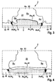
- FIG. 2 shows a schematic representation of intermetallic phases of a thermocompression-bonded gold wire connection on an aluminum bonding surface 19 of an upper side 18 of a semiconductor chip 3.
- FIG. 3 shows a grinding through a corrosion-loaded, unprotected gold bonding wire connection 2 with marking of the corroded intermetallic phases.
- needlehead shape 22 is not much left, it is rather rugged and threatens at least in the left area of the FIG. 3 already to break at the transition to the aluminum coating.
- Such a corrosion process is dependent on the operating time and limits this to a relatively short life for the electronic component.
- the intermetallic first phase Au 4 Al can be seen in the transition from the gold nail head 22 to the aluminum bonding surface 19, and the second intermetallic phase Au 8 Al 3 directly on the silicon surface and the The aluminum-rich third metal phase AuAl 2 surrounding the nail head 22 is still present.
- FIG. 4 shows FIG. 4 a grinding through a corrosion-protected gold bonding wire connection 2 with marking of the intact intermetallic phase structure in an electronic component of the embodiment of the invention according to FIG. 1 , Both the nail head contour in the transition region from the gold wire 20 to the nail head 22 after a tenfold test time compared to the result in FIG. 3 The remaining areas of the intermetallic gold-aluminum phases are still completely intact on the aluminum bonding surface 19.
Landscapes
- Wire Bonding (AREA)
- Structures Or Materials For Encapsulating Or Coating Semiconductor Devices Or Solid State Devices (AREA)
Description
- Die Erfindung betrifft ein elektronisches Bauteil mit korrosionsgeschützter Bondverbindung und ein Verfahren zur Herstellung desselben. Dazu weist das elektronische Bauteil mindestens einen Halbleiterchip auf einem Substrat auf. Ferner ist eine korrosionsgefährdete Bondverbindung auf dem Halbleiterchip vorgesehen. Als Einkapselung des mindestens einen Halbleiterchips und der mindestens einen korrosionsgefährdeten Bondverbindung sind diese von einem hermetisch einschließenden Gehäuse umgeben.
- Aus der Druckschrift
DE10 2008 025 599 A1 sind dazu gehäuste aktive Mikrostrukturen mit Direktkontaktierung zu einem Substrat bekannt. Dazu weist ein mikrostrukturiertes Bauteil aktive Mikrobauelemente, ein Substrat sowie Halbleiterschaltungen auf. Auf dem Substrat ist mindestens ein Gehäuse angeordnet mit einer oder mehreren darin befindlichen aktiven Mikrostrukturen, wobei mindestens eine der aktiven Strukturen durch das sie umgebende Gehäuse hindurch elektrisch an eine elektrische Leiterbahn des Substrats ankontaktiert ist. Das Gehäuse besteht dazu aus einem Bodenelement und einem Deckelement, zwischen denen sich die aktiven Strukturen befinden, wobei das Bodenelement mit dem Deckelement über einen Versiegelungsrahmen verbunden sind. Das Bodenelement und/oder das Deckelement können Vertiefungen aufweisen, in denen ein Gettermaterial angeordnet ist, das bei Aktivierung in definierbarer Weise Gasmoleküle aufnimmt und damit die Gasatmosphäre in dem Gehäuse verändert. Das Gettermaterial kann dazu dienen, Feuchtigkeit zu absorbieren oder Partikel einzufangen. Bei den Kontaktstellen zu den Halbleiterschaltungen kann es sich um Bondflächen handeln. - Aus der Druckschrift
DE 196 03 746 A1 ist ein elektrolumineszierendes Schichtsystem bekannt, das innerhalb des Schichtsystems eine Getterschicht aus einem Gettermetall oder aus einem hykroskopischen Polymer aufweist. Das hygroskopische Polymer weist eine Mischung eines Binderpolymers und einer pulverförmigen hygroskopischen Substanz auf. Die Getterschicht gewährleistet, dass keinerlei Reste von Sauerstoff und/oder Wasser zu dem elektrolumineszierenden Schichtsystem gelangen kann. - Die Verhältnisse bei einem elektronischen Bauteil, das einen Innenraum oder Hohlraum in einem Gehäuse aufweist, in dem unverkapselte Halbleiterbauelemente auf einem Substrat angeordnet sind und in denen Bonddrahtverbindungen auf einem Halbleiterchip der Atmosphäre dieses Innenraums bzw. Hohlraums ausgesetzt sind, sind nicht vergleichbar mit dichtgepackten Schichtsystem, insbesondere dann, wenn Gold-Aluminium-Dünndraht-Bondverbindungen in dem hermetisch abgeschlossenen Gehäuse zu schützen sind, die in dem Schichtsystem weder vorhanden noch zu schützen sind.
- Bekannt ist hingegen, dass bei Verwendung von Silikonen im Innern eines hermetisch einschließenden Gehäuses bei höheren Temperaturen ohne Schutzgasvorkehrungen Wasser entstehen kann. In Verbindung mit kleinsten Mengen an Halogeniden kann das Wasser einen Elektrolyten bilden, der zur Korrosion von Gold-Aluminium-Phasen in Gold-Aluminium-Dünndraht-Bondverbindungen beiträgt und damit zum vorzeitigen Ausfall derartiger Bonddrahtverbindungen führen kann, was die Lebensdauer des elektronischen Bauteils vermindert. In derartigen Fällen werden auch hermetisch abgeschlossene Elektronikverpackungen mit Schutzgas in Form von Helium oder Stickstoff gasdicht befüllt, um den Korrosionsvorgang zu verlangsamen und somit die Lebensdauer derartiger elektronischer Bauteile zu erhöhen.
- Zusätzlich können Gettermetallschichten zur Bindung reaktiver Gase in hermetischen Gehäusen vorgesehen werden, wobei geeignete Gettermetalle wie beispielsweise Kalzium, Lithium oder Strontium aus der Druckschrift
DE 196 03 746 A1 bekannt sind. Derartige Gettermaterialien selbst oder deren Bereitstellung in Getterschichten durch Aufdampfen, Sputtern oder thermisches Aktivieren sind relativ teuer und auch relativ kompliziert zu handhaben. Eine weitere Alternative korrosionsgeschützte Bondverbindungen bereitzustellen, besteht darin, edelmetallhaltige Schutzschichten auf die Aluminium-Metalllegierungen des Halbleiterchips aufzubringen. - In der Durckschrift
DE 100 49 556 A1 wird ein Getter aus Titan verwendet, wobei eine Schicht aus Palladium verhindert, dass sich an der Außenseite des Getters Oxid bildet. - Erfindungsgemäß wird ein elektronisches Bauteil mit korrosionsgeschützter Bondverbindung und ein Verfahren zur Herstellung desselben bereitgestellt. Dazu weist das elektronische Bauteil mindestens einen Halbleiterchip auf einem Substrat auf. Ferner ist eine korrosionsgefährdete Bondverbindung auf dem Halbleiterchip vorgesehen. Als Einkapselung des mindestens einen Halbleiterchips und der mindestens einen korrosionsgefährdeten Bondverbindung sind diese von einem hermetisch einschließenden Gehäuse umgeben. Die hermetisch eingeschlossene Bondverbindung ist eine Bonddrahtverbindung, die vollständig und das Substrat mindestens teilweise in das Gehäuse mit eingeschlossen sind. Das Substrat weist in dem Gehäuse mindestens ein oberflächenmontiertes hydrolyseempfindliches Bauelement auf.
- Durch das Einbringen eines hydrolyseempfindlichen Bauelements kann der Wasseranteil in der Gasatmosphäre des hermetisch geschlossenen Gehäuses durch Hydrolyse eines hydrolyseempfindlichen Materials des hydrolyseempfindlichen Bauelements soweit reduziert werden, dass Wasser für die Bildung von Elektrolyten nicht mehr in ausreichender Menge zur Korrosion der korrosionsgefährdeten Bonddrahtverbindungen zur Verfügung steht.
- In einer weiteren Ausführungsform der Erfindung weist das hydrolyseempfindliche Bauelement eine Oberseite, eine Unterseite und eine zwischen Oberseite und Unterseite angeordnete Randfläche auf, wobei die Unterseite des hydrolyseempfindlichen Bauelements mindestens eine oberflächenmontierbare Molekularlage aufweist. Diese oberflächenmontierbare Molekularlage kann Bestandteil eines Klebstoffes oder eine Molekularlage des hydrolyseempfindlichen Materials des hydrolyseempfindlichen Bauelements sein.
- Weiterhin ist es vorgesehen, dass das hydrolyseempfindliche Bauelement ein hydrolyseempfindliches Kernmaterial aufweist, das Wassermoleküle einer Atmosphäre eines Innenraums des Gehäuses gettert. Das Kernmaterial des hydrolyseempfindlichen Bauelements kann zusätzlich eine semipermeable Beschichtung mindestens auf der Oberseite und der Randfläche des hydrolyseempfindlichen Bauelements aufweisen. Die semipermeable Beschichtung stützt die Form des hydrolyseempfindlichen Bauelements und ist für Wassermoleküle permeabel.
- In einer weiteren Ausführungsform der Erfindung ist es vorgesehen, dass das hydrolyseempfindliche Bauelement einen hydrolyseempfindlichen Kunststoff aufweist. Der hydrolyseempfindliche Kunststoff kann ein hydrolyseempfindliches Polymer sein, das bei seiner Hydrolyse dem Innenraum des Gehäuses Wassermoleküle entzieht. Dabei wird der hydrolyseempfindliche Kunststoff einer intensiven Verseifung durch die Hydrolyse bei Überschreiten einer Glasübergangstemperatur des Kunststoffs ausgesetzt. Eine Verseifung durch Hydrolyse ist die Umkehrreaktion einer Veresterung eines Kunststoffes, sodass als Kunststoff ein hydrolyseempfindlicher Polyester vorgesehen werden kann, der vorzugsweise ein hydrolyseempfindliches Polybutylenterephthalat aufweisen kann.
- Ein Verfahren zur Herstellung eines elektronischen Bauteils mit mindestens einer korrosionsgeschützten Bondverbindung weist die nachfolgenden Verfahrenschritte auf. Zunächst wird mindestens ein Halbleiterchip hergestellt. Dieser Halbleiterchip wird auf ein Substrat aufgebracht. Dann wird mindestens eine Bonddrahtverbindung zwischen dem mindestens einen Halbleiterchip und dem Substrat hergestellt. Außerdem wird ein Oberflächenmontieren mindestens eines Bauelements mit einem hydrolyseempfindlichen Material auf dem Substrat durchgeführt. Danach kann ein hermetisches Einkapseln des mindestens einen Halbleiterchips, der mindestens einen Bonddrahtverbindung, des mindestens einen Bauelements mit dem hydrolyseempfindlichen Material und mindestens teilweise des Substrats in ein Gehäuse durchgeführt werden. Abschließend erfolgt ein Tempern des elektronischen Bauteils bei einer Temperatur über einer Glasumwandlungstemperatur des hydrolyseempfindlichen Materials unter Gettern von Wassermolekülen einer Atmosphäre eines Innenraums des Gehäuses. Dabei kann dieses Tempern auch während des Betriebs des Bauteils erfolgen, wenn die Umgebungstemperaturen des Einsatzortes des Bauteils wie beispielsweise in einem Motorraum eines Kraftfahrzeugs über der Glasumwandlungstemperatur des hydrolyseempfindlichen Materials liegen.
- Beim Aufbringen des mindestens einen Halbleiterchips auf ein Substrat kann auch gleichzeitig das Aufbringen des mindestens einen Bauelements mit dem hydrolyseempfindlichen Material erfolgen, wenn beides über ein stoffschlüssiges Verbinden beispielsweise durch eine Klebstoffschicht auf dem Substrat erfolgen soll. Wenn außerdem die Zuleitungen zu dem elektronischen Bauteil über Durchführungen durch das Gehäuse erfolgen, kann das Substrat nicht nur teilweise sondern auch vollständig in dem hermetisch geschlossenen Gehäuse untergebracht werden. Dabei kann das hermetisch geschlossene Gehäuse aus einem Gehäuseunterteil und einem Gehäusedeckel mit dazwischen angeordnetem gasdichten Verbindungselement zusammengesetzt sein.
- Mit einem derartigen elektronischen Bauteil ist der Vorteil verbunden, dass die korrosionsempfindlichen Bonddrahtverbindungen korrosionsgeschützt werden, die einerseits Goldlegierungsdrähte mit goldbeschichteten Kontaktflächen von beispielsweise Kupferleiterbahnen auf dem Substrat verbinden, und andererseits auf dem Halbleiterchip angeordnete Bondverbindungen des Goldlegierungsdrahtes mit Aluminium-Kontaktflächen auf dem Halbleiterchip herstellen. Dieser Korrosionsschutz wird in vorteilhafter Weise dadurch erreicht, dass durch das auf dem Substrat angeordnete elektrolyseempfindliche Bauelement die Atmosphäre in dem hermetisch geschlossenen Gehäuse an Wassermolekülen derart verarmt, dass halogene Reste in der Atmosphäre des geschlossenen Gehäuses keine korrosiven Elektrolyte mehr bilden können.
- Auf ein Befüllen des hermetisch geschlossenen Gehäuses mit teuren Edelgasen oder Inertgasen kann damit vollständig verzichtet werden. Außerdem vereinfacht sich die Herstellung des Bauteils, da lediglich auf dem Substrat das erfindungsgemäß vorgesehene oberflächenmontierbare elektrolyseempfindliche Bauelement zu fixieren ist. Die semipermeable Beschichtung auf der Oberseite und der Randfläche des elektrolyseempfindlichen Bauelements hat darüber hinaus den Vorteil, dass die durch eine Verseifung der Veresterungen eines Polyesters wie dem Polybutylenterephthalat entstehende Substanz auf das Volumen des hydrolyseempfindlichen Bauelements beschränkt bleibt und sich nicht in dem Innenraum des Gehäuses ausbreiten kann. Das Vorsehen einer adhäsiven Molekularlage beispielsweise einer Klebstoffschicht für die Oberflächenmontage des hydrolyseempfindlichen Bauelements hat den Vorteil, dass eine dauerhafte Fixierung der entstehenden verseiften Substanz auf die Größe der Klebstoffschicht begrenzt bleibt.
- Insbesondere hat das Bauteil den Vorteil, dass die Lebensdauer der Gold-AluminiumVerbindung der Bonddrahtverbindung auf dem Halbleiterchip um eine Zehnerpotenz bei gleichzeitig reduziertem Aufwand für den Korrosionsschutz verbessert werden kann.
- Weitere Aspekte und Vorteile der Erfindung werden nunmehr anhand der beigefügten Figuren eingehender beschrieben. Hierbei zeigt:
- Fig. 1
- eine schematische Darstellung eines elektronischen Bauteils gemäß einer Ausführungsform der Erfindung;
- Fig. 2
- eine Darstellung von intermetallischen Phasen einer Gold-Bonddrahtverbindung auf einem Halbleiterchip;
- Fig. 3
- einen Schliff durch eine korrosionsbelastete, ungeschützte Gold-Bonddrahtverbindung mit Markierung der korrodierten intermetallischen Phasen;
- Fig. 4
- einen Schliff durch eine korrosionsgeschützte Gold-Bonddrahtverbindung des elektronischen Bauteils der Ausführungsform gemäß
Figur 1 . - Die in
Figur 1 gezeigte schematische Darstellung eines elektronischen Bauteils 1 gemäß einer Ausführungsform der Erfindung zeigt ein geschlossenes Gehäuse 5 mit einem Bodenbereich 13 und einem Abdeckbereich 14, wobei der Bodenbereich 13 mit dem Abdeckbereich 14 derart gefügt ist, dass sich ein hermetisch geschlossener Innenraum 12 in dem Gehäuse 5 ergibt. Auf dem Bodenbereich 13 ist mithilfe einer wärmeleitenden Silikonklebstoffschicht 15 ein Substrat 4 aus einer Keramiksubstanz fixiert. Von derartigen Silikonklebstoffschichten 15 ist es bekannt, dass sie bei Temperaturen oberhalb der Raumtemperatur Wassermoleküle in die Atmosphäre des Innenraums 12 emittieren können. Auf einer Oberseite 16 des Substrats 4 ist ein ungehäuster Halbleiterchip 3 mithilfe eines mit silberhaltigen Füllstoffpartikeln gefüllten Epoxidklebers 17 elektrisch leitend fixiert. - Auf einer Oberseite 18 des Halbleiterchips 3 sind Aluminium-Bondflächen 19 aus einer beispielsweise 4 Gew. % siliziumhaltigen Aluminium-Legierung angeordnet, auf denen eine Gold-Bonddrahtverbindung 2 thermokompressionsgebondet ist. Von der Bonddrahtverbindung 2 geht ein Goldbonddraht 20 mit einem Durchmesser zwischen 12 µm bis 50 µm aus und ist mit einem zweiten Ende auf einer Bondfläche 21 mit Goldmetallisierung einer Kupferleiterbahn auf der Oberseite 16 des Substrats 4 fixiert. Die Bonddrahtverbindung 2 auf dem Halbleiterchip 3 ist korrosionsgefährdet, wenn zusätzlich zu einer Wassermoleküle emittierenden Quelle auch eine Halogenide emittierende Störquelle 23 innerhalb des Gehäuses vorhanden ist, so dass sich korrosionsverursachende Elektrolyte bilden können. Um die Bonddrahtverbindung 2 vor einer derartigen Korrosion zu schützen, ist auf der Oberseite 16 des Substrats 4 ein oberflächenmontierbares elektrolyseempfindliches Bauelement 6 angeordnet, das eine Oberseite 7 und eine oberflächenmontierbare Unterseite 8 aufweist.
- Zwischen der Oberseite 7 und der Unterseite 8 ist eine Randfläche 9 angeordnet. Für eine Oberflächenmontage ist mindestens eine molekulare Schicht 10 vorgesehen, die stoffschlüssig das hydrolyseempfindliche Bauelement 6 mit der Oberseite 16 des Substrats 4 verbindet. Das hydrolyseempfindliche Bauelement 6 weist ein Kernmaterial 11 aus einem hydrolyseempfindlichen Material auf, das in dieser Ausführungsform der Erfindung ein Polyester in Form eines Polybutylenterephthalat ist, welches durch die Aufnahme von Wassermolekülen verseift und somit die Atmosphäre des Innenraums 12 des Bauteils 1 an Wassermolekülen verarmt, so dass eine Elektrolytbildung mit Resthalogeniden unterbunden ist. Das Kernmaterial 11 aus einem Polybutylenterephthalat übt somit eine Getterwirkung auf die Wassermoleküle der Gasatmosphäre des Innenraums 12 aus, so dass auf teure alternative Getterschichten oder auf das Auffüllen mit Edelgasen für derartige elektronische Bauteile verzichtet werden kann.
-
Figur 2 zeigt eine schematische Darstellung von intermetallischen Phasen einer thermokompressionsgebondeten Golddrahtverbindung auf einer Aluminium-Bondfläche 19 einer Oberseite 18 eines Halbleiterchips 3. Zunächst ist inFigur 2 die typische Nagelkopfform 22 zu sehen, die beim Thermokompressionsbonden entsteht, wobei sich der runde Golddraht 20 mit einem Durchmesser zwischen 12 und 50 Mikrometern aufgrund einer zwischenzeitlich gebildeten, an dem Golddraht 20 hängenden Schmelzperle aus Gold beim Aufpressen auf die Aluminium-Bondfläche 19 zu der typische Nagelkopfform 22 verformt. Deshalb wird dieses Bondverfahren auch "nail-head-bonding" genannt. Dabei entstehen im Übergang von der Nagelkopfform 22 zu der Aluminium-Bondfläche 19 eine erste intermetallische Phase aus Au4Al und darunter eine zweite intermetallische Phase Au8Al3, die praktisch die gesamte Dicke der Aluminium-Bondfläche aufbraucht. Rings um die Nagelkopfform 22 bildet sich im Übergang zu der Aluminium-Bondfläche 19 eine dritte aluminiumreiche intermetallische Phase AuAl2 aus. Diese thermokompressionsgebondete Bonddrahtverbindung zwischen einem Golddraht 20 und der Aluminium-Bondfläche 19 ist korrosionsgefährdet, was mitFigur 3 gezeigt wird. -
Figur 3 zeigt einen Schliff durch eine korrosionsbelastete, ungeschützte Gold-Bonddrahtverbindung 2 mit Markierung der korrodierten intermetallischen Phasen. Von der ursprünglich inFigur 2 gezeigten Nadelkopfform 22 ist nicht mehr viel übrig, sie ist vielmehr zerklüftet und droht zumindest im linken Bereich derFigur 3 am Übergang zur Aluminiumbeschichtung bereits zu unterbrechen. Ein derartiger Korrosionsvorgang ist abhängig von der Betriebsdauer und begrenzt diese auf eine relativ kurze Lebensdauer für das elektronische Bauteil. Dabei sind auch hier durch die unterschiedlich dunklen Bereiche die intermetallische erste Phase Au4Al im Übergang von dem aus Gold zusammengesetzten Nagelkopf 22 zu der Aluminium-Bondfläche 19 zu erkennen, und auch die zweite intermetallischen Phase Au8Al3 unmittelbar auf der Siliziumoberfläche sowie die den Nagelkopf 22 umgebende aluminiumreiche dritte metallische Phase AuAl2 sind noch vorhanden. - Demgegenüber zeigt
Figur 4 einen Schliff durch eine korrosionsgeschützte Gold-Bonddrahtverbindung 2 mit Markierung der intakten intermetallischen Phasenstruktur in einem elektronischen Bauteil der Ausführungsform der Erfindung gemäßFigur 1 . Sowohl die Nagelkopfkontur in dem Übergangsbereich vom Golddraht 20 zu dem Nagelkopf 22 ist nach einer zehnfachen Testzeit gegenüber dem Ergebnis inFigur 3 noch unverändert erhalten und auch die übrigen Bereiche der intermetallischen Gold-Aluminiumphasen sind auf der Aluminium-Bondfläche 19 noch vollständig intakt.
Claims (8)
- Elektronisches Bauteil mit korrosionsgeschützter Bondverbindung aufweisend:- mindestens einen Halbleiterchip (3) auf einem Substrat (4);- mindestens eine korrosionsgefährdete Bondverbindung auf dem Halbleiterchip (3);- ein den mindestens einen Halbleiterchip (3) und die mindestens eine korrosionsgefährdete Bondverbindung hermetisch einschließendes Gehäuse (5),wobei die Bondverbindung eine Bonddrahtverbindung (2) ist, und wobei die Bonddrahtverbindung (2) vollständig und das Substrat (4) mindestens teilweise in dem Gehäuse (5) hermetisch eingeschlossen ist, und wobei auf dem Substrat (4) mindestens ein oberflächenmontierbares hydrolyseempfindliches Bauelement (6) angeordnet ist, und das hydrolyseempfindliche Bauelement (6) ein hydrolyseempfindliches Kernmaterial (11) aufweist, wobei das Kernmaterial (11) Wassermoleküle einer Atmosphäre eines Innenraumes (12) des Gehäuses (5) geltern kann, wobei das Kernmaterial (11) des hydrolyseempfindlichen Bauelements (6) eine semipermeable Beschichtung mindestens auf der Oberseite (7) und der Randfläche (9) des hydrolyseempfindlichen Bauelements (6) aufweist, und wobei die semipermeable Beschichtung die Form des hydrolyseempfindlichen Bauelements (6) bei Vesseifung und Fernverlust stützt und für Wassermoleküle permeabel ist.
- Elektronisches Bauteil nach Anspruch 1, wobei das hydrolyseempfindliche Bauelement (6) eine Oberseite (7), eine Unterseite (8) und eine zwischen Oberseite (7) und Unterseite (8) angeordnete Randfläche (9) aufweist, und wobei die Unterseite (8) des hydrolyseempfindlichen Bauelements (6) eine oberflächenmontierbare Molekularlage (10) aufweist.
- Elektronisches Bauteil nach einem der vorhergehenden Ansprüche, wobei das hydrolyseempfindliche Bauelement (6) einen hydrolyseempfindlichen Kunststoff aufweist.
- Elektronisches Bauteil nach Anspruch 3, wobei der Kunststoff ein hydrolyseempfindliches Polymer, das bei seiner Hydrolyse dem Innenraum (12) des Gehäuses (5) Wassermoleküle entzieht, aufweist.
- Elektronisches Bauteil nach Anspruch 3 oder Anspruch 4, wobei der hydrolyseempfindliche Kunststoff eine intensive Verseifung durch Hydrolyse bei Überschreiten einer Glasübergangstemperatur des Kunststoffs aufweist.
- Elektronisches Bauteil nach einem der Ansprüche 3 bis 5, wobei der Kunststoff ein hydrolyseempfindlicher Polyester ist.
- Elektronisches Bauteil nach einem der Ansprüche 3 bis 6, wobei der Kunststoff ein hydrolyseempfindliches Polybutylenterephthalat ist.
- Verfahren zur Herstellung eines elektronischen Bauteils (1) gemäß einem der vorhergehenden Ansprüche, das nachfolgende Verfahrenschritte aufweist:- Herstellen mindestens eines Halbleiterchips (3);- Aufbringen des mindestens einen Halbleiterchips (3) auf ein Substrat (4);- Herstellen mindestens einer Bonddrahtverbindung (2) zwischen dem mindestens einen Halbleiterchip (3) und dem Substrat (4);- Oberflächenmontieren mindestens eines Bauelements (6) mit einem hydrolyseempfindlichen Material auf dem Substrat (4);- hermetisches Einkapseln des mindestens einen Halbleiterchips (3), der mindestens einen Bonddrahtverbindung (2), des mindestens einen Bauelements (6) mit dem hydrolyseempfindlichen Material und mindestens teilweise des Substrats (4) in ein Gehäuse (5);- Tempern des elektronischen Bauteils (1) bei einer Temperatur über einer Glasumwandlungstemperatur des hydrolyseempfindlichen Materials unter Gettern von Wassermolekülen einer Atmosphäre eines Innenraums (12) des Gehäuses (5),wobei das hydrolyseempfindliche Bauelement (6) ein hydrolyseempfindliches Kernmaterial (11) aufweist, wobei das Kernmaterial (11) des hydrolyseempfindlichen Bauelements (6) eine semipermeable Beschichtung mindestens auf der Oberseite (7) und der Randfläche (9) des hydrolyseempfindlichen Bauelements (6) aufweist, und wobei die semipermeable Beschichtung die Form des hydrolyseempfindlichen Bauelements (6) bei Verseifung und Formverlust stützt und für Wassermoleküle permeabel ist.
Applications Claiming Priority (2)
| Application Number | Priority Date | Filing Date | Title |
|---|---|---|---|
| DE201210200273 DE102012200273A1 (de) | 2012-01-11 | 2012-01-11 | Elektronisches Bauteil mit korrosionsgeschützter Bondverbindung und Verfahren zur Herstellung des Bauteils |
| PCT/EP2012/073971 WO2013104460A1 (de) | 2012-01-11 | 2012-11-29 | Elektronisches bauteil mit korrosionsgeschützter bondverbindung und verfahren zur herstellung des bauteils |
Publications (2)
| Publication Number | Publication Date |
|---|---|
| EP2803082A1 EP2803082A1 (de) | 2014-11-19 |
| EP2803082B1 true EP2803082B1 (de) | 2016-02-03 |
Family
ID=47326106
Family Applications (1)
| Application Number | Title | Priority Date | Filing Date |
|---|---|---|---|
| EP12798672.7A Not-in-force EP2803082B1 (de) | 2012-01-11 | 2012-11-29 | Elektronisches bauteil mit korrosionsgeschützter bondverbindung und verfahren zur herstellung des bauteils |
Country Status (6)
| Country | Link |
|---|---|
| US (1) | US9425118B2 (de) |
| EP (1) | EP2803082B1 (de) |
| JP (1) | JP5955412B2 (de) |
| CN (1) | CN104054170B (de) |
| DE (1) | DE102012200273A1 (de) |
| WO (1) | WO2013104460A1 (de) |
Families Citing this family (5)
| Publication number | Priority date | Publication date | Assignee | Title |
|---|---|---|---|---|
| JP6354467B2 (ja) * | 2014-09-01 | 2018-07-11 | 株式会社デンソー | 半導体装置 |
| JP5669335B1 (ja) * | 2014-09-26 | 2015-02-12 | 田中電子工業株式会社 | 銀金合金ボンディングワイヤ |
| US9844169B2 (en) * | 2014-10-31 | 2017-12-12 | The Johns Hopkins University | Ka band multi-chip modulator |
| US10998275B2 (en) | 2016-12-30 | 2021-05-04 | Intel Corporation | Package with cathodic protection for corrosion mitigation |
| CN113327882B (zh) * | 2021-05-21 | 2024-09-24 | 通富微电子股份有限公司 | 一种半导体器件封装用吸嘴及封装系统、封装方法 |
Family Cites Families (15)
| Publication number | Priority date | Publication date | Assignee | Title |
|---|---|---|---|---|
| US4382327A (en) * | 1979-09-17 | 1983-05-10 | Beckman Instruments, Inc. | Method for particle entrapment within an electrical device package |
| JPS5938643A (ja) | 1982-08-27 | 1984-03-02 | Murata Mfg Co Ltd | 温度センサ |
| FR2538618B1 (fr) * | 1982-12-28 | 1986-03-07 | Inf Milit Spatiale Aeronaut | Boitier pour composant electronique comportant un element fixant l'humidite |
| DE19603746A1 (de) | 1995-10-20 | 1997-04-24 | Bosch Gmbh Robert | Elektrolumineszierendes Schichtsystem |
| JP2001168240A (ja) | 1999-10-08 | 2001-06-22 | Trw Inc | 集積型マイクロエレクトロニクスモジュール |
| JP3936151B2 (ja) * | 2000-05-08 | 2007-06-27 | 双葉電子工業株式会社 | 有機el素子 |
| JP2002212268A (ja) * | 2001-01-19 | 2002-07-31 | Japan Epoxy Resin Kk | 半導体封止用エポキシ樹脂組成物 |
| US7560820B2 (en) * | 2004-04-15 | 2009-07-14 | Saes Getters S.P.A. | Integrated getter for vacuum or inert gas packaged LEDs |
| JP2007231453A (ja) | 2006-03-01 | 2007-09-13 | Teijin Fibers Ltd | 感湿捲縮複合繊維 |
| JP2007242243A (ja) * | 2006-03-03 | 2007-09-20 | Seiko Epson Corp | 有機半導体装置および電子機器 |
| JP2007305811A (ja) * | 2006-05-12 | 2007-11-22 | Matsushita Electric Ind Co Ltd | 半導体装置および半導体装置の製造方法 |
| JP2009088115A (ja) * | 2007-09-28 | 2009-04-23 | Shin Etsu Chem Co Ltd | 車載用電気電子部品 |
| DE102008024599A1 (de) | 2008-05-21 | 2009-12-10 | WINKLER+DüNNEBIER AG | Vorrichtung zur Bildung von Stapelpaketen |
| JPWO2010095367A1 (ja) * | 2009-02-19 | 2012-08-23 | 日本電気株式会社 | 真空封止パッケージ、真空封止パッケージを有するプリント回路基板、電子機器、及び真空封止パッケージの製造方法 |
| JP2011026556A (ja) * | 2009-06-25 | 2011-02-10 | Jsr Corp | 組成物、硬化体、および電子デバイス |
-
2012
- 2012-01-11 DE DE201210200273 patent/DE102012200273A1/de not_active Withdrawn
- 2012-11-29 EP EP12798672.7A patent/EP2803082B1/de not_active Not-in-force
- 2012-11-29 CN CN201280066623.8A patent/CN104054170B/zh not_active Expired - Fee Related
- 2012-11-29 WO PCT/EP2012/073971 patent/WO2013104460A1/de not_active Ceased
- 2012-11-29 US US14/370,858 patent/US9425118B2/en not_active Expired - Fee Related
- 2012-11-29 JP JP2014551543A patent/JP5955412B2/ja not_active Expired - Fee Related
Also Published As
| Publication number | Publication date |
|---|---|
| US9425118B2 (en) | 2016-08-23 |
| CN104054170A (zh) | 2014-09-17 |
| JP2015503851A (ja) | 2015-02-02 |
| JP5955412B2 (ja) | 2016-07-20 |
| DE102012200273A1 (de) | 2013-07-11 |
| EP2803082A1 (de) | 2014-11-19 |
| US20150137391A1 (en) | 2015-05-21 |
| CN104054170B (zh) | 2017-03-15 |
| WO2013104460A1 (de) | 2013-07-18 |
Similar Documents
| Publication | Publication Date | Title |
|---|---|---|
| DE102011053871B4 (de) | Multichip-Halbleitergehäuse und deren Zusammenbau | |
| EP0202279B1 (de) | Verfahren zum einkapseln von mikroelektronischen halbleiter- und schichtschaltungen | |
| EP2349672B1 (de) | Verfahren zur herstellung eines geschwindigkeits-sensorelements | |
| DE69330607T2 (de) | Kunststoff-halbleiterpackung mit aluminium-waermesenke | |
| DE102013102973B4 (de) | Halbleiterpackages und Verfahren zu deren Ausbildung | |
| EP1602625B1 (de) | Halbleitermodul mit einem Halbleiter-Sensorchip und einem Kunststoffgehäuse sowie Verfahren zu dessen Herstellung | |
| DE102009051342A1 (de) | Mikroelektronisches Gehäuse und Verfahren zum Anordnen in einem Gehäuse | |
| DE19518753A1 (de) | Halbleitervorrichtung und Verfahren zu ihrer Herstellung | |
| DE102019130778A1 (de) | Ein Package, welches ein Chip Kontaktelement aus zwei verschiedenen elektrisch leitfähigen Materialien aufweist | |
| EP2803082A1 (de) | Elektronisches bauteil mit korrosionsgeschützter bondverbindung und verfahren zur herstellung des bauteils | |
| DE10351761A1 (de) | Sensor für eine dynamische Grösse | |
| DE102014100196A1 (de) | Verfahren zum elektrophoretischen Abscheiden (EPD) eines Films auf einer exponierten leitfähigen Oberfläche und ein elektrisches Bauteil daraus | |
| DE69418184T2 (de) | Verfahren zur verbindung von halbleiterchips mit einem substrat | |
| DE102017220258B4 (de) | Halbleitersensorbauelement und Verfahren zum Herstellen desselben | |
| WO1999033106A1 (de) | Kunststoffverbundkörper | |
| DE102008045033A1 (de) | Erhöhte Drahtverbindungsstabilität auf reaktiven Metalloberflächen eines Halbleiterbauelements durch Einkapselung der Verbindungsstruktur | |
| DE102006056361B4 (de) | Modul mit polymerhaltigem elektrischen Verbindungselement und Verfahren | |
| DE102008039939B4 (de) | Integriertes Schaltungsbauelement mit einer aus der Gasphase abgeschiedenen Isolationsschicht und Verfahren zu seiner Herstellung | |
| DE102019120051B4 (de) | Package mit selektivem Korrosionsschutz einer elektrischen Verbindungsstruktur | |
| WO2023169904A1 (de) | Mikromechanisches bauelement und entsprechendes herstellungsverfahren | |
| DE10042839A1 (de) | Elektronisches Bauteil mit Wärmesenke und Verfahren zu seiner Herstellung | |
| JPH05315474A (ja) | 電子部品及びその製造方法 | |
| DE102014112025A1 (de) | Eingehauste Halbleitervorrichtung | |
| JPS62105459A (ja) | 半導体構造物 | |
| DE68927771T2 (de) | Verfahren zur Herstellung einer Elektronik-Packung |
Legal Events
| Date | Code | Title | Description |
|---|---|---|---|
| PUAI | Public reference made under article 153(3) epc to a published international application that has entered the european phase |
Free format text: ORIGINAL CODE: 0009012 |
|
| 17P | Request for examination filed |
Effective date: 20140811 |
|
| AK | Designated contracting states |
Kind code of ref document: A1 Designated state(s): AL AT BE BG CH CY CZ DE DK EE ES FI FR GB GR HR HU IE IS IT LI LT LU LV MC MK MT NL NO PL PT RO RS SE SI SK SM TR |
|
| DAX | Request for extension of the european patent (deleted) | ||
| GRAP | Despatch of communication of intention to grant a patent |
Free format text: ORIGINAL CODE: EPIDOSNIGR1 |
|
| INTG | Intention to grant announced |
Effective date: 20150813 |
|
| GRAS | Grant fee paid |
Free format text: ORIGINAL CODE: EPIDOSNIGR3 |
|
| GRAA | (expected) grant |
Free format text: ORIGINAL CODE: 0009210 |
|
| AK | Designated contracting states |
Kind code of ref document: B1 Designated state(s): AL AT BE BG CH CY CZ DE DK EE ES FI FR GB GR HR HU IE IS IT LI LT LU LV MC MK MT NL NO PL PT RO RS SE SI SK SM TR |
|
| REG | Reference to a national code |
Ref country code: GB Ref legal event code: FG4D Free format text: NOT ENGLISH |
|
| REG | Reference to a national code |
Ref country code: AT Ref legal event code: REF Ref document number: 774051 Country of ref document: AT Kind code of ref document: T Effective date: 20160215 Ref country code: CH Ref legal event code: EP |
|
| REG | Reference to a national code |
Ref country code: IE Ref legal event code: FG4D Free format text: LANGUAGE OF EP DOCUMENT: GERMAN |
|
| REG | Reference to a national code |
Ref country code: DE Ref legal event code: R096 Ref document number: 502012005937 Country of ref document: DE |
|
| REG | Reference to a national code |
Ref country code: LT Ref legal event code: MG4D Ref country code: NL Ref legal event code: MP Effective date: 20160203 |
|
| PG25 | Lapsed in a contracting state [announced via postgrant information from national office to epo] |
Ref country code: FI Free format text: LAPSE BECAUSE OF FAILURE TO SUBMIT A TRANSLATION OF THE DESCRIPTION OR TO PAY THE FEE WITHIN THE PRESCRIBED TIME-LIMIT Effective date: 20160203 Ref country code: HR Free format text: LAPSE BECAUSE OF FAILURE TO SUBMIT A TRANSLATION OF THE DESCRIPTION OR TO PAY THE FEE WITHIN THE PRESCRIBED TIME-LIMIT Effective date: 20160203 Ref country code: GR Free format text: LAPSE BECAUSE OF FAILURE TO SUBMIT A TRANSLATION OF THE DESCRIPTION OR TO PAY THE FEE WITHIN THE PRESCRIBED TIME-LIMIT Effective date: 20160504 Ref country code: NO Free format text: LAPSE BECAUSE OF FAILURE TO SUBMIT A TRANSLATION OF THE DESCRIPTION OR TO PAY THE FEE WITHIN THE PRESCRIBED TIME-LIMIT Effective date: 20160503 |
|
| PG25 | Lapsed in a contracting state [announced via postgrant information from national office to epo] |
Ref country code: IS Free format text: LAPSE BECAUSE OF FAILURE TO SUBMIT A TRANSLATION OF THE DESCRIPTION OR TO PAY THE FEE WITHIN THE PRESCRIBED TIME-LIMIT Effective date: 20160603 Ref country code: RS Free format text: LAPSE BECAUSE OF FAILURE TO SUBMIT A TRANSLATION OF THE DESCRIPTION OR TO PAY THE FEE WITHIN THE PRESCRIBED TIME-LIMIT Effective date: 20160203 Ref country code: NL Free format text: LAPSE BECAUSE OF FAILURE TO SUBMIT A TRANSLATION OF THE DESCRIPTION OR TO PAY THE FEE WITHIN THE PRESCRIBED TIME-LIMIT Effective date: 20160203 Ref country code: PL Free format text: LAPSE BECAUSE OF FAILURE TO SUBMIT A TRANSLATION OF THE DESCRIPTION OR TO PAY THE FEE WITHIN THE PRESCRIBED TIME-LIMIT Effective date: 20160203 Ref country code: LT Free format text: LAPSE BECAUSE OF FAILURE TO SUBMIT A TRANSLATION OF THE DESCRIPTION OR TO PAY THE FEE WITHIN THE PRESCRIBED TIME-LIMIT Effective date: 20160203 Ref country code: LV Free format text: LAPSE BECAUSE OF FAILURE TO SUBMIT A TRANSLATION OF THE DESCRIPTION OR TO PAY THE FEE WITHIN THE PRESCRIBED TIME-LIMIT Effective date: 20160203 Ref country code: SE Free format text: LAPSE BECAUSE OF FAILURE TO SUBMIT A TRANSLATION OF THE DESCRIPTION OR TO PAY THE FEE WITHIN THE PRESCRIBED TIME-LIMIT Effective date: 20160203 Ref country code: PT Free format text: LAPSE BECAUSE OF FAILURE TO SUBMIT A TRANSLATION OF THE DESCRIPTION OR TO PAY THE FEE WITHIN THE PRESCRIBED TIME-LIMIT Effective date: 20160603 |
|
| PG25 | Lapsed in a contracting state [announced via postgrant information from national office to epo] |
Ref country code: EE Free format text: LAPSE BECAUSE OF FAILURE TO SUBMIT A TRANSLATION OF THE DESCRIPTION OR TO PAY THE FEE WITHIN THE PRESCRIBED TIME-LIMIT Effective date: 20160203 Ref country code: DK Free format text: LAPSE BECAUSE OF FAILURE TO SUBMIT A TRANSLATION OF THE DESCRIPTION OR TO PAY THE FEE WITHIN THE PRESCRIBED TIME-LIMIT Effective date: 20160203 |
|
| REG | Reference to a national code |
Ref country code: DE Ref legal event code: R097 Ref document number: 502012005937 Country of ref document: DE |
|
| REG | Reference to a national code |
Ref country code: FR Ref legal event code: PLFP Year of fee payment: 5 |
|
| PG25 | Lapsed in a contracting state [announced via postgrant information from national office to epo] |
Ref country code: RO Free format text: LAPSE BECAUSE OF FAILURE TO SUBMIT A TRANSLATION OF THE DESCRIPTION OR TO PAY THE FEE WITHIN THE PRESCRIBED TIME-LIMIT Effective date: 20160203 Ref country code: SK Free format text: LAPSE BECAUSE OF FAILURE TO SUBMIT A TRANSLATION OF THE DESCRIPTION OR TO PAY THE FEE WITHIN THE PRESCRIBED TIME-LIMIT Effective date: 20160203 Ref country code: CZ Free format text: LAPSE BECAUSE OF FAILURE TO SUBMIT A TRANSLATION OF THE DESCRIPTION OR TO PAY THE FEE WITHIN THE PRESCRIBED TIME-LIMIT Effective date: 20160203 Ref country code: SM Free format text: LAPSE BECAUSE OF FAILURE TO SUBMIT A TRANSLATION OF THE DESCRIPTION OR TO PAY THE FEE WITHIN THE PRESCRIBED TIME-LIMIT Effective date: 20160203 |
|
| PLBE | No opposition filed within time limit |
Free format text: ORIGINAL CODE: 0009261 |
|
| STAA | Information on the status of an ep patent application or granted ep patent |
Free format text: STATUS: NO OPPOSITION FILED WITHIN TIME LIMIT |
|
| 26N | No opposition filed |
Effective date: 20161104 |
|
| PG25 | Lapsed in a contracting state [announced via postgrant information from national office to epo] |
Ref country code: SI Free format text: LAPSE BECAUSE OF FAILURE TO SUBMIT A TRANSLATION OF THE DESCRIPTION OR TO PAY THE FEE WITHIN THE PRESCRIBED TIME-LIMIT Effective date: 20160203 Ref country code: BE Free format text: LAPSE BECAUSE OF NON-PAYMENT OF DUE FEES Effective date: 20161130 Ref country code: BG Free format text: LAPSE BECAUSE OF FAILURE TO SUBMIT A TRANSLATION OF THE DESCRIPTION OR TO PAY THE FEE WITHIN THE PRESCRIBED TIME-LIMIT Effective date: 20160503 |
|
| REG | Reference to a national code |
Ref country code: CH Ref legal event code: PL |
|
| GBPC | Gb: european patent ceased through non-payment of renewal fee |
Effective date: 20161129 |
|
| PG25 | Lapsed in a contracting state [announced via postgrant information from national office to epo] |
Ref country code: CH Free format text: LAPSE BECAUSE OF NON-PAYMENT OF DUE FEES Effective date: 20161130 Ref country code: LI Free format text: LAPSE BECAUSE OF NON-PAYMENT OF DUE FEES Effective date: 20161130 |
|
| REG | Reference to a national code |
Ref country code: IE Ref legal event code: MM4A |
|
| PG25 | Lapsed in a contracting state [announced via postgrant information from national office to epo] |
Ref country code: LU Free format text: LAPSE BECAUSE OF NON-PAYMENT OF DUE FEES Effective date: 20161130 |
|
| REG | Reference to a national code |
Ref country code: FR Ref legal event code: PLFP Year of fee payment: 6 |
|
| PG25 | Lapsed in a contracting state [announced via postgrant information from national office to epo] |
Ref country code: GB Free format text: LAPSE BECAUSE OF NON-PAYMENT OF DUE FEES Effective date: 20161129 Ref country code: IE Free format text: LAPSE BECAUSE OF NON-PAYMENT OF DUE FEES Effective date: 20161129 |
|
| REG | Reference to a national code |
Ref country code: BE Ref legal event code: MM Effective date: 20161130 |
|
| PG25 | Lapsed in a contracting state [announced via postgrant information from national office to epo] |
Ref country code: ES Free format text: LAPSE BECAUSE OF FAILURE TO SUBMIT A TRANSLATION OF THE DESCRIPTION OR TO PAY THE FEE WITHIN THE PRESCRIBED TIME-LIMIT Effective date: 20160203 Ref country code: HU Free format text: LAPSE BECAUSE OF FAILURE TO SUBMIT A TRANSLATION OF THE DESCRIPTION OR TO PAY THE FEE WITHIN THE PRESCRIBED TIME-LIMIT; INVALID AB INITIO Effective date: 20121129 |
|
| PG25 | Lapsed in a contracting state [announced via postgrant information from national office to epo] |
Ref country code: CY Free format text: LAPSE BECAUSE OF FAILURE TO SUBMIT A TRANSLATION OF THE DESCRIPTION OR TO PAY THE FEE WITHIN THE PRESCRIBED TIME-LIMIT Effective date: 20160203 Ref country code: MK Free format text: LAPSE BECAUSE OF FAILURE TO SUBMIT A TRANSLATION OF THE DESCRIPTION OR TO PAY THE FEE WITHIN THE PRESCRIBED TIME-LIMIT Effective date: 20160203 Ref country code: MC Free format text: LAPSE BECAUSE OF FAILURE TO SUBMIT A TRANSLATION OF THE DESCRIPTION OR TO PAY THE FEE WITHIN THE PRESCRIBED TIME-LIMIT Effective date: 20160203 |
|
| PG25 | Lapsed in a contracting state [announced via postgrant information from national office to epo] |
Ref country code: MT Free format text: LAPSE BECAUSE OF FAILURE TO SUBMIT A TRANSLATION OF THE DESCRIPTION OR TO PAY THE FEE WITHIN THE PRESCRIBED TIME-LIMIT Effective date: 20160203 |
|
| PG25 | Lapsed in a contracting state [announced via postgrant information from national office to epo] |
Ref country code: TR Free format text: LAPSE BECAUSE OF FAILURE TO SUBMIT A TRANSLATION OF THE DESCRIPTION OR TO PAY THE FEE WITHIN THE PRESCRIBED TIME-LIMIT Effective date: 20160203 Ref country code: AL Free format text: LAPSE BECAUSE OF FAILURE TO SUBMIT A TRANSLATION OF THE DESCRIPTION OR TO PAY THE FEE WITHIN THE PRESCRIBED TIME-LIMIT Effective date: 20160203 |
|
| REG | Reference to a national code |
Ref country code: AT Ref legal event code: MM01 Ref document number: 774051 Country of ref document: AT Kind code of ref document: T Effective date: 20171129 |
|
| PG25 | Lapsed in a contracting state [announced via postgrant information from national office to epo] |
Ref country code: AT Free format text: LAPSE BECAUSE OF NON-PAYMENT OF DUE FEES Effective date: 20171129 |
|
| PGFP | Annual fee paid to national office [announced via postgrant information from national office to epo] |
Ref country code: FR Payment date: 20211119 Year of fee payment: 10 |
|
| PGFP | Annual fee paid to national office [announced via postgrant information from national office to epo] |
Ref country code: IT Payment date: 20211130 Year of fee payment: 10 |
|
| PGFP | Annual fee paid to national office [announced via postgrant information from national office to epo] |
Ref country code: DE Payment date: 20220125 Year of fee payment: 10 |
|
| REG | Reference to a national code |
Ref country code: DE Ref legal event code: R119 Ref document number: 502012005937 Country of ref document: DE |
|
| PG25 | Lapsed in a contracting state [announced via postgrant information from national office to epo] |
Ref country code: IT Free format text: LAPSE BECAUSE OF NON-PAYMENT OF DUE FEES Effective date: 20221129 Ref country code: DE Free format text: LAPSE BECAUSE OF NON-PAYMENT OF DUE FEES Effective date: 20230601 |
|
| PG25 | Lapsed in a contracting state [announced via postgrant information from national office to epo] |
Ref country code: FR Free format text: LAPSE BECAUSE OF NON-PAYMENT OF DUE FEES Effective date: 20221130 |