EP2774152B1 - Integrierte mischspannungsschaltung mit nichtflüchtigem speicher mit energieeinsparung - Google Patents
Integrierte mischspannungsschaltung mit nichtflüchtigem speicher mit energieeinsparung Download PDFInfo
- Publication number
- EP2774152B1 EP2774152B1 EP12846107.6A EP12846107A EP2774152B1 EP 2774152 B1 EP2774152 B1 EP 2774152B1 EP 12846107 A EP12846107 A EP 12846107A EP 2774152 B1 EP2774152 B1 EP 2774152B1
- Authority
- EP
- European Patent Office
- Prior art keywords
- terminal
- voltage
- pmos transistor
- circuit
- gate
- Prior art date
- Legal status (The legal status is an assumption and is not a legal conclusion. Google has not performed a legal analysis and makes no representation as to the accuracy of the status listed.)
- Active
Links
Images






Classifications
-
- G—PHYSICS
- G11—INFORMATION STORAGE
- G11C—STATIC STORES
- G11C16/00—Erasable programmable read-only memories
- G11C16/02—Erasable programmable read-only memories electrically programmable
- G11C16/06—Auxiliary circuits, e.g. for writing into memory
- G11C16/30—Power supply circuits
-
- G—PHYSICS
- G11—INFORMATION STORAGE
- G11C—STATIC STORES
- G11C16/00—Erasable programmable read-only memories
- G11C16/02—Erasable programmable read-only memories electrically programmable
- G11C16/06—Auxiliary circuits, e.g. for writing into memory
- G11C16/08—Address circuits; Decoders; Word-line control circuits
-
- G—PHYSICS
- G11—INFORMATION STORAGE
- G11C—STATIC STORES
- G11C5/00—Details of stores covered by group G11C11/00
- G11C5/14—Power supply arrangements, e.g. power down, chip selection or deselection, layout of wirings or power grids, or multiple supply levels
- G11C5/147—Voltage reference generators, voltage or current regulators; Internally lowered supply levels; Compensation for voltage drops
-
- G—PHYSICS
- G11—INFORMATION STORAGE
- G11C—STATIC STORES
- G11C11/00—Digital stores characterised by the use of particular electric or magnetic storage elements; Storage elements therefor
- G11C11/56—Digital stores characterised by the use of particular electric or magnetic storage elements; Storage elements therefor using storage elements with more than two stable states represented by steps, e.g. of voltage, current, phase, frequency
- G11C11/5621—Digital stores characterised by the use of particular electric or magnetic storage elements; Storage elements therefor using storage elements with more than two stable states represented by steps, e.g. of voltage, current, phase, frequency using charge storage in a floating gate
- G11C11/5628—Programming or writing circuits; Data input circuits
Definitions
- the present invention relates to an integrated circuit die for receiving a plurality of different voltages and more particularly wherein the die has the capability to save power.
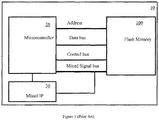
- FIG. 1 there is shown a block diagram of a flash (non-volatile) memory integrated circuit die 10 of the prior art.
- the flash memory circuit die 10 comprises a flash memory array 100, having a plurality of flash memory cells arranged in a plurality of rows and columns.
- a microcontroller 20 controls the operation of the flash array 100 through an address bus, a data bus and a control bus.
- a mixed IP circuit 30 controls both the microcontroller 20 and the array 100 through a mixed signal bus.
- the microcontroller 20 is supplied with a voltage source of 3.0 volts
- the flash array 100 is supplied with a voltage source of 1.8 volts.
- the 1.8 volt source is generated by the mixed IP circuit 30 using a DC-DC converter based upon an externally supplied 3.0 volt source.
- the externally supplied 3.0 volt source is also supplied to the microcontroller 20.
- FIG. 2 there is shown a schematic block level circuit diagram 60 of a portion of the flash memory circuit die 10 shown in Figure 1 .
- the circuit diagram has a die pad 21 connected through bond wire 51 to a bond pad 41 for receiving the externally supplied 3.0 volts.
- the externally supplied 3.0 volts is then supplied in the die 10 to IO buffer circuit 36, and to other well known circuits, such as TTL circuit 34 (converting input signal voltage level to CMOS voltage level), POR3V circuit 32 (detecting Vdd reaching a pre-determined voltage level), and other circuits not shown .
- TTL circuit 34 converting input signal voltage level to CMOS voltage level
- POR3V circuit 32 detecting Vdd reaching a pre-determined voltage level
- These circuits require 3.0 volts for operation.
- the 3.0 volt source is also supplied to a DC-DC voltage regulator 30 from which a source of 1.8 volts is generated.
- the 1.8 volt source is then supplied to other parts of the die 10, described hereinabo
- certain circuit blocks (not shown) inside the flash memory 100 need not be powered during certain chip operation such as during erase or programming operation, read circuits can be on standby and during read operation, erase and programming circuits can be on standby. Reducing and/or eliminating power to portions of the circuit in the die 10 that do not require power can reduce the total power requirements of the integrated circuit die 10.
- US 6,005,802 A discloses a nonvolatile semiconductor memory device including a memory cell section including at least one nonvolatile memory cell, a first bit line connected to one end of the memory cell section, and a second bit line capacitively coupled with the first bit line.
- the first bit line is set to a first voltage, thereafter rendered electrically floating, the voltage of the second bit line is changed to a second voltage after the first bit line is rendered electrically floating, and then the first bit line which is set in the electrically floating state is capacitively coupled with second bit line to change the voltage of the first bit line to a third voltage higher than the first and second voltages.
- US 2007/047365 A1 provides a semiconductor device supplied with internal power generated by an internal power generation circuit to perform a stable operation and, also, suppress power consumption.
- a control circuit, a row/column decoder and a sense amplifier are driven by an internal buck voltage.
- a data path with high power consumption is driven by an external power supply voltage.
- a level conversion circuit receives an address signal or a command signal having a voltage level of the external power supply voltage, converts the voltage level to the internal buck voltage, and outputs a resultant signal to the control circuit.
- a level conversion circuit receives a control signal having a voltage level of the internal buck voltage from the control circuit, converts the voltage level to the external power supply voltage, and outputs a resultant signal to the data path.
- a semiconductor integrated circuit includes a first circuit and a second circuit having a breakdown voltage higher than a breakdown voltage of the first circuit, and operation voltages of the first and second circuits can be made equal to each other or different from each other.
- the second circuit has a plurality of level shift circuits capable of shifting the level of an output of the first circuit in accordance with an operation voltage of the second circuit, a plurality of external output buffers receiving outputs of the level shift circuits, bypasses for bypassing an input of a predetermined level shift circuit to an input of a predetermined external output buffer, and a selecting circuit for selecting connection of either the predetermined level shift circuit or a bypass to an input of the predetermined external output buffer.
- the bypass is selected. In high-voltage operation and burn
- US 2004/190346 A1 provides a differential non-volatile memory device that includes setting means, at least first and second OTP memory cells that are each coupled between a supply voltage and a reference voltage, and a read circuit forming a first current path between the first memory cell and the reference voltage and a second current path between the second memory cell and the reference voltage for reading the bit and the complementary bit that are stored in the first and second memory cells.
- the first current path includes a first circuit point that is associated with a first output terminal
- the second current path includes a second circuit point that is associated with a second output terminal.
- the setting means can be activated to bring the first and second circuit points to a voltage value that is substantially equal to the reference voltage, and is able to set the value of the current flowing through each of the first and second current paths. Also provided is a method for reading such a differential non-volatile memory device.
- US 2004/125663 A1 discloses that a regulated charge pump, regulated by a plurality of capacitor boost stages and separate from the memory device supply voltage (Vcc), generates a regulated voltage (VSA) over a range of supply voltages.
- the regulated charge pump powers sense amplifier and differential amplifier circuits of the memory device to permit a low bit line bias voltage.
- the differential amplifier circuit generates a logical output to indicate a memory cell programmed state that is detected by the sense amplifier circuit.
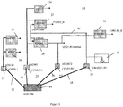
- the circuit 62 has four (internal) die pads 23, 25, 27, 29.
- the circuit 62 has one bond pad: 42.
- Bond pad is an external pad such as a package pad (which connecting to a package pin).
- Die pad 23 and 25 connect to bond pad 42 through bonding wires (52 & 54).
- Die pads 23 and 25 receive a first voltage source, Vdd1, of 3.0 volts, although any voltage within 3.0V specification tolerance (such as 2.2V to 4.0V) can be supplied.
- Die pad 27 receives a second voltage source, Vdd2, of 1.8 volts, which is less than the first voltage source.
- the Vdd2 is supplied from the DC-DC regulator 30 in this case. Again however, any voltage source within 1.8V specification tolerance (such as 1.2V to 2.0V) can be provided.
- Die pad 29 is left floating, hence it gets pulled down to ground through the resistor in block 46, in this embodiment.
- the voltage from the bond pad 42 is supplied to the IO buffer circuit 36, to the charge pump circuit 38, and to other well known circuits (such as the TTL circuit 34, the POR3V circuit 32), all described heretofore, that require 3.0 volts for operation.
- the 3.0 volt is also supplied to a DC-DC voltage regulator 30 from which a source of 1.8 volts is generated.
- the 1.8 volt source is then supplied to other parts of the die 10, described hereinabove, such as the flash memory array 100.
- the current sensing circuit 46 senses no current flow in this case, which generates a control signal 48 in response thereto.
- the control signal 48 is supplied to the DC-DC voltage regulator 30 and is used to control the operation of the regulator 30, as described hereinbelow.
- the voltage source Vdd2 is supplied to the internal circuits of the die 10 that requires operation using the voltage Vdd2.
- the die 10 In the operation of the die 10 with the circuit 62, the die 10 must have been designed such that circuits that require the use of voltage source Vdd1 are never on at the same time as the circuits that require the voltage from Vdd2. Thus, 3.0 volt transistors or other circuit elements are operational only at a certain point in time, which is before vdd2 being operational, while transistors and other circuit elements are only operational at other points in time. In that event, assuming that only circuit elements requiring Vdd1 are on, then the externally supplied Vdd1 supplies the voltage Vdd1 to the various circuit elements in the die 10.
- the DC-DC voltage regulator 30 is enabled, because the current sensing element 46 does not detect any current flow (die pad 29 is float thus no current supplied to the circuit 46).
- the control signal 48 enables the DC-DC regulator 30.
- the source of the voltage Vdd2 is supplied from the DC-DC regulator 30.
- FIG. 4 there is shown a circuit diagram 63 of a second embodiment. Similar to the embodiment shown in Figure 3 , the circuit 63 has four die pads 23, 25, 27, 29 and two bond pad 42 and 43. In this configuration die pads 23 and 25 are connected through bond wires 52 and 54 to the bond pad 42 and die pads 27 and 29 are connected through bond wires 56 and 58 to bond pad 43 respectively.
- Bond pad 42 receives a first voltage source, Vdd1, of 3.0 volts, although any voltage can be supplied.
- Bond pad 43 receives a second voltage source, Vdd2, of 1.8 volts, which is less than the first voltage source. Again however, any voltage source can be supplied.
- the sensing circuit 46 now detects current flow since die pad 29 receives a voltage from bond pad 43.
- control signal 48 which disables the DC-DC regulator 30.
- the 3V circuits operate with the 3.0 volts from the Vdd1 bond pad 42 and the 1.8V circuits operate with 1.8 volts from the Vdd2 bond pad 43.
- the voltage from the bond pad 42 is supplied to the IO buffer circuit 36, to the charge pump circuit 38, and to other well known circuits, all described heretofore, that require 3.0 volts for operation.
- the 1.8 volt source is supplied to other parts of the die 10, described hereinabove, such as the flash memory array 100.
- FIG. 5 there is shown a circuit diagram 64 of a third embodiment. Similar to the embodiment shown in Figure 3 , the circuit 64 has four die pads 23, 25, 27, 29 and one bond pad 44. In this configuration all die pads 23, 25, 27, and 29 are connected through bond wires 52, 54, 56, and 58 respectively to bond pad 44. Bond pad 44 receives a voltage source, Vdd2, of 1.8 volts externally. The circuit 46 now detects current flow since die pad 29 receives a voltage from bond pad 44. This in turn activates the control signal 48 which disable the DC-DC regulator 30. In this embodiment al1 the circuits operate with the 1.8 volts from the Vdd2 bond pad 44. In this case the TTL circuit 34, IOBUF circuit 36, and charge pump 38 are to operate at 1.8V supply.
- Vdd2 voltage source
- circuit diagram 66 of a fourth embodiment Similar to the embodiment shown in Figure 3 , the circuit 64 has four die pads 23, 25, 27, and 28 and one bond pad 46. In this configuration die pads 23 and 25 are connected through bond wires 52 and 54 to bond pad 46. Bond pad 46 receives a voltage source of 3.0 volts from Vdd1.
- the voltage from the bond pad 46 is supplied to the IO buffer circuit 36, to the charge pump circuit 38, and to other well known circuits, all described heretofore, that require 3.0 volts for operation.
- the 3.0 volt is also supplied to a DC-DC voltage regulator 30 from which a source of 1.8 volts is generated.
- the 1.8 volt source is then supplied to other parts of the die 10, described hereinabove, such as the flash memory array 100.
- the 3.0 volt is also supplied to a DC-DC voltage regulator 31 from which a source of 1.8 volts is generated which is supplied to the sensing circuitry of the flash memory.
- a configuration bit is used to enable the DC-DC regulator 30 and 31.
- the configuration bit is supplied by the microcontroller 20 or by an initialization sequence at power up (similar to that described by Figures 8 and 9 ).
- the die 10 In the operation of the die 10 with the circuit 66, the die 10 must have been designed such that circuits that require the use of voltage source Vdd1 are connected to the voltage source Vdd1, while those circuits that are only periodically or intermittently operations using Vdd2 are connected to the first voltage regulator 30. All other circuits that require Vdd2, but which can be on at the same time as circuits that require Vdd1, are connected to the second voltage regulator 31.
- the flash array memory cells 100 are connected to the voltage regulator 30, while circuit elements in the sense amplifier that require Vdd2 are connected to the voltage regulator 31.
- circuit elements that require Vdd2 operation but not at the same time as circuit elements that require Vdd1 operation operate from the regulator 30 as described hereinabove.
- the source of Vdd2 is the regulator 31. In this manner, the benefits of power saving as described hereinabove is achieved, even though some circuit elements requiring Vdd2 are operational at the same time as those circuit elements that require Vdd1.
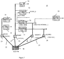
- FIG. 7 there is shown a circuit diagram 68 of a fifth embodiment. Similar to the embodiment shown in Figure 3 , the circuit 64 has four die pads 23, 25, 27, and 28 and one bond pad 46. In this configuration die pads 23, 25, 27, and 28 are connected through bond wires 52, 54, 56, and 59 respectively to bond pad 46. Bond pad 46 receives a voltage source, Vdd2, of 1.8 volts. In this embodiment all circuits need to be operational at 1.8 volts. In this embodiment a configuration bit is used to disable the DC-DC regulator 30 and 31. The configuration bit is supplied by the microcontroller 20 or by a initialization sequence at power up (similar to that described by Figures 8 and 9 ).
- Figure 8 is a mixed power supply power sequence flow and timing.
- the fuse bits are used as configuration bits for chip operation. Chip operation includes operations such as various power saving modes and non-volatile operation modes (erase, program, read, testing, etc).
- the power up sequence flow is also called a fusebit recall sequence (or flow).
- a certain configuration bits are for configuring the die pad connection such as for power supplies 3V and 1.8V.
- a certain configuration bits are for configuring the circuits such as to work properly with power supplies 3V and 1.8V.
- a 3V power detection circuit is monitored to check if 3V supply is ramp up to a certain trip point (e.g., 2.2V), then a 1.8V power detection circuit is monitored to check if 1.8V supply is ramp up to a certain trip point (e.g., 1.3V).
- a complementary (inverted data on same patter and on next pattern, such as "1" and "0") fixed pattern check is used to determine if the chip operation is reliable (e.g., reading AAAA/5555/FFFE/0001 data pattern). If the fixed pattern check is true then fuse bits are recalled (configuration bits) to set up chip configurations.
- a concurrent pattern check (such as A/5 pattern and/or parity bits) is used at the same time recalling the fuse bits to ensure the fuse recalling is reliable.
- an embedded pattern (such as A/5 pattern and/or parity bit) within each fuse word (e.g., 16 fuse bits for each fuse word) is implemented to ensure fuse recall is reliable.
- An embodiment is A(Fs ⁇ 7:0>)5/5(Fs ⁇ 7:0>A for 16 bits recall, Fs ⁇ 7:0> is fuse bits, A and 5 are alternating pattern bits for consecutive recalling, Another embodiment is 1(Fs ⁇ 13:0>)0/0(Fs ⁇ 13:0>)1 with 1,0 are alternating pattern bits for consecutive recalling.
- the fixed pattern check is used again to ensure again the chip operation is reliable. If this post pattern check is true then the power up recall operation is done.
- margining adapting trip point of sensing or timing adjustment
- parity bits are done for pattern bits and fuse bits to ensure another layer of reliability check.
- multiple memory cells are used for each fuse bit for operational reliability.
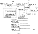
- FIG. 9 shows a block diagram 600 of a power sequence controller for power up sequence and fuse bit (configuration bits) recall timing.
- Block 620 is a DC-DC regulator to provide 1.8V from a 3.0V supply. It consists of a 1.8V LDO (linear regulator VDDREGp 1.8V) and a soft regulator Soft-vddreg 1.8V.
- the linear regulator VDDREGp 1.8V provides (hard) precise regulation for normal operation.
- the soft regulator is used to provide approximate 1.2-1.8v during power up when the VDDREGp 1.8V is not operational yet or during power saving mode (smaller voltage level than the level during normal operation).
- Block 610 POR3V is to provide trip point for 3V Supply.
- Block 630 POR1.8V is to provide trip point for 1.8V Supply.
- Block 640 PORLOG is used to provide logic during power up.
- Block 666 PWRCALL is used to provide fuse recall logic control.
- the signal sequence is POR3V_N then POR1.8V_N and finally POR_N (combing POR3V_N and POR1.8V_N).
- FIG. 15 shows a power operating embodiment for the flash chip 100 for further efficient power utilization of the flash chip with operation mode of Standby, Deep Power Down, Read, Program and Erase operation with power supply availability of 3V and 1.8V.
- the power operating embodiment of various circuit functional blocks are enabled by, for example, configuration bits in the fusebit recall flow of the power sequence.
- Vdd power supply
- Vdd for charge pump hv circuitry
- Vdd for Logic Controller 3V and/or 1.8V
- Vdd for x-decoding (aka row decoder) is 3V and/or 1.8V
- Vdd for y-decoding circuitry (aka column decoder) is 1.8V and/or 3V
- Vdd for IOBUF is 3V
- voltage level for the VDDREG1.8V output is 1.8V (hard (accurate) regulation mode block 620, also hard power level).
- Vdd power supply
- Vdd for charge pump hv circuitry
- Vdd for Logic Controller is either 3V and/or 1.3-1.6V
- Vdd for x-decoding aka row decoder
- Vdd for y-decoding circuitry aka column decoder
- Vdd for IOBUF 3V
- voltage level for the VDDREG1.8V output is 1.3-1.6V (soft regulation mode block 620 Figure 9 , also soft power level).
- Vdd power supply for sensing circuitry is (1.8V and/or 3V)/0V/0V respectively
- Vdd for charge pump (hv circuitry) is 0V/3V/3V respectively
- Vdd for Logic Controller is 3V and/or 1.8V for Read/Prog/Erase
- Vdd for x-decoding (aka row decoder) is 1.8V for Read/Prog/Erase
- Vdd for y-decoding circuitry (aka column decoder) is 1.8V and/or 3V for Read/Prog/Erase
- Vdd for IOBUF is 3V
- voltage level for the VDDREG1.8V output is 1.8V (hard (accurate) regulation mode block 620 Figure 9 ) for Read/Prog/Erase.
- FIG. 15 shows a power operating embodiment for the flash chip 100 for further efficient power utilization of the flash chip with operation mode of Standby, Deep Power Down, Read, Program and Erase operation with power supply availability of 1.8V.
- Standby Mode Vdd (power supply) for sensing circuitry is 0V
- Vdd for charge pump (hv circuitry) is 0V
- Vdd for Logic Controller is 1.8V
- Vdd for x-decoding (aka row decoder) is 1.8V
- Vddd for y-decoding circuitry (aka column decoder) is 0V
- Vdd for IOBUF is 1.8V
- voltage level for the VDDREG1.8V output is 1.8V.
- Vdd power supply
- Vdd for charge pump hv circuitry
- Vdd for Logic Controller 1.8V
- Vdd for x-decoding 0V
- Vdd for y-decoding circuitry 0V
- Vdd for IOBUF 1.8V
- voltage level for the VDDREG1.8V output is 1.0-1.3V (soft regulation mode block 620 Figure 9 ).
- Vdd power supply for sensing circuitry is 1.8V/0V/0V respectively
- Vdd for charge pump (hv circuitry) is 0V/1.8V/1.8V respectively
- Vdd for Logic Controller is 1.8V for Read/Prog/Erase
- Vdd for x-decoding (aka row decoder) is 1.8V for Read/Prog/Erase
- Vdd for y-decoding circuitry (aka column decoder) is 1.8V for Read/Prog/Erase
- Vdd for IOBUF is 1.8V
- voltage level for the VDDREG1.8V output is 1.8V (accurate regulation mode block 620 Figure 9 ) for Read/Prog/Erase.
- the sense amplifier 760 is of a Mixed Power Supply Mixed Oxide Pseudo Differential Amplifying scheme.
- Mixed power supply refers to multiple supplies, e.g. 3v (or 5V) and 1.8v and/or 1.2V, being used on same sense amplifier.
- Mixed oxide refers to multiple oxides (e.g, 3v (or 5V) and 1.8v oxides (and/or 1.2V oxide)) being used in same sense amplifier.
- the sense amplifier 760 receives the voltage Vdd1 of approximately 3.0 volts along the first bus 762, and the voltage Vdd2 of approximately 1.8 volts (or 1.2V alternatively) along the second bus 764.
- the first bus 762 is connected to PMOS transistors 770(a-c),that belongs to first legs of the sense amplifier (also known as the (memory) read out circuit).
- the transistors 770(a-c) are also called the pullup (load) transistors of the read out circuit
- the first leg of the sense amplifier 760 includes first leg for reference column (SAL REF 792) and data columns (SAL0-N 794) NMOS transistors 780(a-c) serves as cascoding amplifying function for the first leg circuitry.
- PMOS transistors 790(a-b) serves to clamp the voltage level at sensed output node (drain of transistor 770(a-c)) less than approximately 2V to avoid stressing (or breaking down) the gate oxide of the next leg of the sense amplifier (circuitry connected to bus 764).
- the second bus 764 is connected to all of the rest of the PMOS transistors in the sense amplifier 760.
- the transistors 770(a-c) that receive the voltage of Vdd1 have thicker (gate) oxides (3V oxide, e.g., 70 Angstrom) than the rest of the transistors that receive the voltage of Vdd2 (1.8V oxide, e.g., 32 Angstrom).
- the transistors 770(a-c) are 1.8V transistors (1.8V oxide) since the voltage drop across its terminals (nodes) are to be operated to be less than a pre-determined voltage, .e.g. 2V to avoid breakdown from 1.8V oxide.
- Similar transistors 780(a-c) can be implemented as 3V transistors or 1.8V transistors. In the 1.8v oxide case, voltage drop across its terminals are to be operated to be less than a pre-determined voltage to avoid breakdown from 1.8V oxide.
- the Pseudo Differential Amplifier 760 works as follows.
- the first leg of the reference column SAL_REF 792 converts the memory cell current into a current mirror by the action of the diode connected PMOS transistor 770c, the reference current is now mirrored by the transistor 770c (though bias voltage on its drain) into the gate of the PMOS transistors 780(a-d) of the data column SAL_0-N 794.
- Vdd1 supplied on the first leg of the sense amplifier (also known as the readout circuit)
- the dynamic operating range of the sense amplifier is much larger compared to that of the 1.8V power supply.
- the second leg of the sense amplifier, DIFA0-N 798 uses 1.8v power supply (Vdd2) to convert the sensed node (drain of the transistor 780d) into a digital voltage level (output VOUT0-N) '0' or '1' depending on the memory cell current DATA0-N 'high' or 'low' respectively and to accomplish the 3V to 1.8V voltage level conversion at the same times.
- the second leg DIFA0-N 798 uses 1.8V power supply, hence 1,8v transistors can be used here (smaller area and higher performance vs. 3v transistors).
- the differential amplifier 798 which is made of all 1.8v transistors, consists of input stage NMOS 721 & 722 and PMOS load 723 & 724 and bias NMOS 727.
- the second stage consists of PMOS 725 and NMOS 726 to convert into digital output VOUTD.
- Switches S1 702 is for initialization before sensing.
- the input transistors 721 and 722 are 3.0v transistors instead of 1.8v transistors, for example, in case the clamp transistors 790(a-b) are not used.
- the ymux (y decoder) are not shown in Figures 10-13 for the sense amplifiers for brevity, The ymux is used to select the memory cell columns (bitlines) to connect the selected memory cells to the sense amplifiers.
- the sense amplifier 761 is similar to the sense amplifier 760 with the exception of the transistor 781c and 782c (hence the rest of the transistors are the same).
- the readout circuit 792 utilizes the transistor 781c and 782c in a drain-gate-isolation closed loop source follower configuration on the output node (drain of the pullup transistor 770c or drain of the cascode transistor 780c) to extend the dynamic range of the read out circuit.
- the drain-gate-isolation refers to isolation of the drain and gate nodes of the pullup load transistor.
- the transistor 781c is native NMOS transistor (approximately zero threshold voltage) serves to isolate the drain and gate of the transistor 770c.
- the drain of the transistor 770c now can go higher than its gate voltage allowing for wider dynamic range for the cascoding transistor 780c (its drain can go higher voltage than previously).
- the transistor 782c serves as bias current for the transistor 781c.
- the gate of the transistor 770c is also the source of the transistor 781c (acts as source follower) and effectively this node is now low impedance (meaning can drive higher current, leading to higher speed).
- This technique can be used for reading out the data cell in addition to reading out the reference cell. This technique can be used on the other sensing circuits in Figures 12 and 13 .
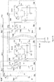
- the sense amplifier 860 is of a Differential Amplifying scheme.
- the sense amplifier 860 receives the voltage Vdd1 of approximately 3.0 volts along the first bus 762, and the voltage Vdd2 of approximately 1.8 volts along the second bus 764.
- the first bus 762 is connected to PMOS transistors 870(a-c) and 871 (a-c).
- the second bus 764 is connected to all of the rest of the PMOS transistors in the sense amplifier 860.
- the transistors 870(a-c) and 871(a-c) that receive the voltage of Vdd1 have thicker oxides than the rest of the transistors that receive the voltage of Vdd2.
- the Differential Amplifier 860 works as follows.
- the first leg of the sense amplifier includes first leg for reference column (SAL REF 892) and data columns (SAL0-N 894) NMOS transistors 880(a-c) serves as cascoding amplifying function for the first leg circuitry.
- the reference cell voltage and data cell voltage are then compared by the differential amplifiers 898 to convert into a digital output VOUTD.
- sense amplifier 760 by partitioning the sense amplifier into the readout circuit (892, 894) operating at 3V resulting into higher dynamic range and a differential amplifier (898) operating at a lower voltage (e.g., 1.8V) resulting into smaller area and higher speed.
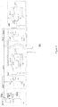
- the sense amplifier 960 is of a Single Ended Amplifying scheme.
- the sense amplifier 960 receives the voltage Vdd1 of approximately 3.0 volts along the first bus 762, and the voltage Vdd2 of approximately 1.8 volts along the second bus 764.
- the first bus 762 is connected to PMOS transistors 870(a-c) and 871(a-c).
- the second bus 764 is connected to all of the rest of the PMOS transistors in the sense amplifier 960.
- the transistors 870(a-c) and 871(a-c) that receive the voltage of Vdd1 have thicker oxides than the rest of the transistors that receive the voltage of Vdd2.
- the Sense Amplifier 960 works as follows.
- the first leg of the sense amplifier includes first leg for reference column (SAL REF 892) and data columns (SAL0-N 994) NMOS transistors 880(a-c) serves as cascoding amplifying function for the first leg circuitry.
- PMOS transistors 870(a-c) serves as pullup loading and mirror cell current into PMOS transistors 871(a-c).
- the reference cell current is then converted into reference voltage by NMOS transistors 872c.
- This reference cell voltage then mirror the cell current into the transistor 872a of the data column 994.
- This mirrored reference cell current is than compared versus the data cell current from transistor 871a.
- the current comparison output is the drain voltage of the transistor 871a.
- the single ended amplifier 998 consists of first stage of PMOS transistor 974 and NMOS 975 with current bias 976 and 977 respectively.
- PMOS 973 is weak feedback transistor.
- NMOS 972 is isolation transistor isolating 3V from 1.8V voltage.
- the second stage consists of PMOS 978 and NMOS 979. Switches 962 S1 and 964 S2 are for initialization before sensing.
- the advantage of the sense amplifier 960 is higher dynamic range for readout circuit 892, and 994 and smaller area and power for single ended amplifier 998 (versus sense amplifier 860 and 760 having differential amplifier on the second leg).
- the circuit 1000 comprises an IO predriver circuit 1010, and two driver circuits 1020a and 1020b.
- the predriver circuit 1010 receives the data output 1002 from the memory cell(s) and directs the signal to either the output driver circuit 1020a or the output driver circuit 1020b.
- Switches 1004(a-c) route the data output signal 1002 to either the driver circuit 1020a or driver circuit 1020b.
- the difference between the driver circuit 1020a and driver circuit 1020b is that the driver circuit 1020a is powered by 3.0 volts while the driver output circuit 1020b is powered by 1.8 volts.
- the 3.0 volt driver circuit 1020a serves as an ESD protection circuit for the 1.8 volt driver circuit 1020b.
Landscapes
- Engineering & Computer Science (AREA)
- Power Engineering (AREA)
- Read Only Memory (AREA)
- Semiconductor Integrated Circuits (AREA)
- Dram (AREA)
- Semiconductor Memories (AREA)
Claims (5)
- Nichtflüchtige Flash-Speichervorrichtung als integrierte Schaltung, die Folgendes umfasst:eine Anordnung nichtflüchtiger Flash-Speicherzellen;einen Leseverstärker (860), der mit der Anordnung nichtflüchtiger Flash-Speicherzellen verbunden ist, wobei der Leseverstärker eine Referenzspalte (892), eine Datenspalte (894) und einen Differenzverstärker (898) umfasst,wobei die Referenzspalte Folgendes umfasst:einen ersten PMOS-Transistor (870c), der einen ersten Anschluss, einen zweiten Anschluss und ein Gate umfasst,einen ersten NMOS-Transistor (880c), der einen ersten Anschluss, der an den zweiten Anschluss des ersten PMOS-Transistors (870c) gekoppelt ist, einen zweiten Anschluss und ein Gate umfasst,eine Referenzschaltung (REF), die an den zweiten Anschluss des ersten NMOS-Transistors (880c) gekoppelt ist,einen zweiten PMOS-Transistor (871c), der einen ersten Anschluss, einen zweiten Anschluss und ein Gate, das an das Gate und den zweiten Anschluss des ersten PMOS-Transistors (870c) gekoppelt ist, umfasst, undeinen zweiten NMOS-Transistor (872c), der einen ersten Anschluss, der an den zweiten Anschluss des zweiten PMOS-Transistors (871c) gekoppelt ist, einen zweiten Anschluss, der an Masse gekoppelt ist, und ein Gate, das an den zweiten Anschluss des zweiten PMOS-Transistors (871c) und an einen ersten Eingang des Differenzverstärkers gekoppelt ist, umfasst, undwobei die Datenspalte umfasst:einen dritten PMOS-Transistor (870a), der einen ersten Anschluss, einen zweiten Anschluss und ein Gate umfasst,einen dritten NMOS-Transistor (880a), der einen ersten Anschluss, der an den zweiten Anschluss des dritten PMOS-Transistors (870a) gekoppelt ist, einen zweiten Anschluss und ein Gate umfasst,eine nichtflüchtige Flash-Speicherzelle (DATA0...N) in der Anordnung von nichtflüchtigen Flash-Speicherzellen, die an den zweiten Anschluss des dritten NMOS-Transistors (880a) gekoppelt ist,einen vierten PMOS-Transistor (871a), der einen ersten Anschluss, einen zweiten Anschluss und ein Gate, das an das Gate und den zweiten Anschluss des dritten PMOS-Transistors (870a) gekoppelt ist, umfasst, undeinen vierten NMOS-Transistor (872a), der einen ersten Anschluss, der an den zweiten Anschluss des vierten PMOS-Transistors (871a) gekoppelt ist, einen zweiten Anschluss, der an Masse gekoppelt ist, und ein Gate, das an den zweiten Anschluss des vierten PMOS-Transistors (871a) und einen zweiten Eingang des Differenzverstärkers gekoppelt ist, umfasst;eine erste Spannungsquelle (762), die an den ersten Anschluss des ersten PMOS-Transistors (870c), den ersten Anschluss des zweiten PMOS-Transistors (871c), den ersten Anschluss des dritten PMOS-Transistors (870a) und den ersten Anschluss des vierten PMOS-Transistors (871a) gekoppelt ist; undeine zweite Spannungsquelle (764), die von der ersten Spannungsquelle verschieden ist und die an den Differenzverstärker gekoppelt ist;wobei der Differenzverstärker konfiguriert ist, einen durch die Datenspalte gezogenen Strom und einen durch die Referenzspalte gezogenen Strom zu vergleichen, um ein Digitalspannungsniveau zu erzeugen, das die in der nichtflüchtigen Flash-Speicherzelle in der Datenspalte gespeicherten Daten angibt.
- Vorrichtung nach Anspruch 1, wobei die Datenspalte und die Referenzspalte jeweils Transistoren mit einem ersten Gate-Oxid umfassen.
- Vorrichtung nach Anspruch 3, wobei der Differenzverstärker Transistoren mit einem zweiten Gate-Oxid umfasst, wobei das zweite Gate-Oxid eine Dicke besitzt, die von der Dicke des ersten Gate-Oxids verschieden ist.
- Vorrichtung nach Anspruch 3, wobei der Differenzverstärker eine geklemmte Ausgangsspannung bei dem Ausgangsknoten aufweist, um eine Belastung oder einen Ausfall des zweiten Gate-Oxids zu verhindern.
- Vorrichtung nach Anspruch 3, wobei die Referenzspalte Transistoren (781c und 782c) in einer Source-Folger-Konfiguration mit geschlossenem Regelkreis und Drain-Gate-Isolation umfasst.
Applications Claiming Priority (2)
| Application Number | Priority Date | Filing Date | Title |
|---|---|---|---|
| US13/286,969 US8705282B2 (en) | 2011-11-01 | 2011-11-01 | Mixed voltage non-volatile memory integrated circuit with power saving |
| PCT/US2012/059808 WO2013066592A2 (en) | 2011-11-01 | 2012-10-11 | A mixed voltage non-volatile memory integrated circuit with power saving |
Publications (3)
| Publication Number | Publication Date |
|---|---|
| EP2774152A2 EP2774152A2 (de) | 2014-09-10 |
| EP2774152A4 EP2774152A4 (de) | 2015-07-08 |
| EP2774152B1 true EP2774152B1 (de) | 2019-07-31 |
Family
ID=48172294
Family Applications (1)
| Application Number | Title | Priority Date | Filing Date |
|---|---|---|---|
| EP12846107.6A Active EP2774152B1 (de) | 2011-11-01 | 2012-10-11 | Integrierte mischspannungsschaltung mit nichtflüchtigem speicher mit energieeinsparung |
Country Status (7)
| Country | Link |
|---|---|
| US (2) | US8705282B2 (de) |
| EP (1) | EP2774152B1 (de) |
| JP (1) | JP5830176B2 (de) |
| KR (1) | KR101485308B1 (de) |
| CN (3) | CN107093441B (de) |
| TW (2) | TWI497276B (de) |
| WO (1) | WO2013066592A2 (de) |
Families Citing this family (14)
| Publication number | Priority date | Publication date | Assignee | Title |
|---|---|---|---|---|
| US9124276B2 (en) * | 2012-12-20 | 2015-09-01 | Qualcomm Incorporated | Sense amplifier including a level shifter |
| US9417675B2 (en) * | 2014-05-29 | 2016-08-16 | Silicon Storage Technology, Inc. | Power sequencing for embedded flash memory devices |
| US10452594B2 (en) | 2015-10-20 | 2019-10-22 | Texas Instruments Incorporated | Nonvolatile logic memory for computing module reconfiguration |
| US10043578B2 (en) * | 2015-11-12 | 2018-08-07 | Mediatek Inc. | Sense amplifier circuits |
| US10331203B2 (en) * | 2015-12-29 | 2019-06-25 | Texas Instruments Incorporated | Compute through power loss hardware approach for processing device having nonvolatile logic memory |
| JP2018133503A (ja) * | 2017-02-16 | 2018-08-23 | 東芝メモリ株式会社 | 半導体記憶装置 |
| US10388335B2 (en) * | 2017-08-14 | 2019-08-20 | Micron Technology, Inc. | Sense amplifier schemes for accessing memory cells |
| DE102018131711B3 (de) | 2018-12-11 | 2020-06-10 | Infineon Technologies Ag | Abtastschaltung und Abtastverfahren |
| EP3710257B1 (de) | 2019-02-06 | 2021-09-08 | Hewlett-Packard Development Company, L.P. | Schreiben eines nichtflüchtigen speichers auf programmierte ebenen |
| US11036581B2 (en) * | 2019-08-08 | 2021-06-15 | Apple Inc. | Non-volatile memory control circuit with parallel error detection and correction |
| TWI714475B (zh) * | 2020-03-17 | 2020-12-21 | 華邦電子股份有限公司 | 控制裝置以及記憶體系統 |
| CN113448424B (zh) * | 2020-03-27 | 2023-12-08 | 华邦电子股份有限公司 | 控制装置以及存储器系统 |
| WO2022027403A1 (en) * | 2020-08-06 | 2022-02-10 | Yangtze Memory Technologies Co., Ltd. | Multi-die peak power management for three-dimensional memory |
| CN120199291B (zh) * | 2025-05-26 | 2025-07-25 | 西安智多晶微电子有限公司 | 一种fpga片上非易失性存储器的供电电路 |
Citations (4)
| Publication number | Priority date | Publication date | Assignee | Title |
|---|---|---|---|---|
| US20030137340A1 (en) * | 2002-01-18 | 2003-07-24 | Hitachi, Ltd. | Semiconductor integrated circuit and a burn-in method thereof |
| US20040125663A1 (en) * | 2002-12-26 | 2004-07-01 | Micron Technology, Inc. | Low voltage sense amplifier for operation under a reduced bit line bias voltage |
| US20040190346A1 (en) * | 2003-03-04 | 2004-09-30 | Stmicroelectronics S.R.L. | Differential non-volatile memory device and bit reading method for the same |
| US20080080257A1 (en) * | 2006-09-29 | 2008-04-03 | Hynix Semiconductor Inc. | Flash memory device and its reading method |
Family Cites Families (37)
| Publication number | Priority date | Publication date | Assignee | Title |
|---|---|---|---|---|
| JPH0297058A (ja) * | 1988-10-03 | 1990-04-09 | Mitsubishi Electric Corp | 半導体記憶装置 |
| JPH03110650A (ja) * | 1989-09-25 | 1991-05-10 | Casio Comput Co Ltd | Eepromチェック方式 |
| US5519654A (en) * | 1990-09-17 | 1996-05-21 | Kabushiki Kaisha Toshiba | Semiconductor memory device with external capacitor to charge pump in an EEPROM circuit |
| JPH04205887A (ja) * | 1990-11-30 | 1992-07-28 | Hitachi Ltd | 半導体集積回路装置 |
| US5103425A (en) | 1991-03-11 | 1992-04-07 | Motorola, Inc. | Zener regulated programming circuit for a nonvolatile memory |
| JPH0684996A (ja) * | 1992-09-07 | 1994-03-25 | Nec Corp | 半導体装置 |
| JPH0729386A (ja) * | 1993-07-13 | 1995-01-31 | Hitachi Ltd | フラッシュメモリ及びマイクロコンピュータ |
| JPH08125034A (ja) | 1993-12-03 | 1996-05-17 | Mitsubishi Electric Corp | 半導体記憶装置 |
| US5661690A (en) | 1996-02-27 | 1997-08-26 | Micron Quantum Devices, Inc. | Circuit and method for performing tests on memory array cells using external sense amplifier reference current |
| US5646890A (en) | 1996-03-29 | 1997-07-08 | Aplus Integrated Circuits, Inc. | Flexible byte-erase flash memory and decoder |
| JPH10144079A (ja) * | 1996-11-07 | 1998-05-29 | Mitsubishi Electric Corp | 半導体記憶装置 |
| JP4046383B2 (ja) * | 1997-04-01 | 2008-02-13 | 株式会社ルネサステクノロジ | 半導体集積回路装置 |
| KR100554112B1 (ko) | 1997-05-30 | 2006-02-20 | 미크론 테크놀로지,인코포레이티드 | 256 메가 다이내믹 랜덤 액세스 메모리 |
| JP3425340B2 (ja) * | 1997-10-09 | 2003-07-14 | 株式会社東芝 | 不揮発性半導体記憶装置 |
| US6009023A (en) * | 1998-05-26 | 1999-12-28 | Etron Technology, Inc. | High performance DRAM structure employing multiple thickness gate oxide |
| JP4530464B2 (ja) * | 2000-03-09 | 2010-08-25 | ルネサスエレクトロニクス株式会社 | 半導体集積回路 |
| JP2001266572A (ja) * | 2000-03-17 | 2001-09-28 | Fujitsu Ltd | 半導体集積回路 |
| WO2002082460A1 (en) * | 2001-04-02 | 2002-10-17 | Hitachi, Ltd. | Semiconductor non-volatile storage device |
| JP2002373495A (ja) * | 2001-06-14 | 2002-12-26 | Hitachi Ltd | 半導体チップ、半導体集積回路装置及び半導体集積回路装置の製造方法 |
| TW546840B (en) * | 2001-07-27 | 2003-08-11 | Hitachi Ltd | Non-volatile semiconductor memory device |
| US6924702B2 (en) * | 2003-06-17 | 2005-08-02 | Taiwan Semiconductor Manufacturing Co., Ltd. | Low supply voltage and self-biased high speed receiver |
| EP1566809B1 (de) * | 2004-02-19 | 2006-11-29 | STMicroelectronics S.r.l. | Abfühlschaltung mit regulierter Referenzspannung |
| JP4703133B2 (ja) * | 2004-05-25 | 2011-06-15 | ルネサスエレクトロニクス株式会社 | 内部電圧発生回路および半導体集積回路装置 |
| KR100674936B1 (ko) * | 2005-01-10 | 2007-01-26 | 삼성전자주식회사 | 강화된 파우워를 갖는 반도체 메모리장치 및 이의 파우워강화 방법 |
| US7864615B2 (en) * | 2005-02-25 | 2011-01-04 | Kingston Technology Corporation | Flash memory controller utilizing multiple voltages and a method of use |
| US7499307B2 (en) * | 2005-06-24 | 2009-03-03 | Mosys, Inc. | Scalable embedded DRAM array |
| US7355905B2 (en) * | 2005-07-01 | 2008-04-08 | P.A. Semi, Inc. | Integrated circuit with separate supply voltage for memory that is different from logic circuit supply voltage |
| EP1905084A2 (de) * | 2005-07-08 | 2008-04-02 | Nxp B.V. | Integrierte schaltung mit schutz vor elektrostatischen entladungen |
| JP2007066463A (ja) | 2005-09-01 | 2007-03-15 | Renesas Technology Corp | 半導体装置 |
| US7394637B2 (en) * | 2005-12-15 | 2008-07-01 | Taiwan Semiconductor Manufacturing Co., Ltd. | Sense amplifier with leakage compensation for electrical fuses |
| US20070247915A1 (en) * | 2006-04-21 | 2007-10-25 | Intersil Americas Inc. | Multiple time programmable (MTP) PMOS floating gate-based non-volatile memory device for a general-purpose CMOS technology with thick gate oxide |
| KR100781984B1 (ko) * | 2006-11-03 | 2007-12-06 | 삼성전자주식회사 | 셀프 레퍼런스를 갖는 센스앰프 회로 및 그에 의한 센싱방법 |
| US7738306B2 (en) * | 2007-12-07 | 2010-06-15 | Etron Technology, Inc. | Method to improve the write speed for memory products |
| US7751250B2 (en) * | 2008-06-27 | 2010-07-06 | Sandisk Corporation | Memory device with power noise minimization during sensing |
| US8325554B2 (en) * | 2008-07-10 | 2012-12-04 | Sanmina-Sci Corporation | Battery-less cache memory module with integrated backup |
| US7764563B2 (en) * | 2008-11-26 | 2010-07-27 | Micron Technology, Inc. | Adjustable voltage regulator for providing a regulated output voltage |
| CN101924536B (zh) * | 2009-06-12 | 2012-05-02 | 昂宝电子(上海)有限公司 | 用于ccfl驱动系统的突发模式调光控制的低频振荡器 |
-
2011
- 2011-11-01 US US13/286,969 patent/US8705282B2/en active Active
-
2012
- 2012-10-11 CN CN201610844224.XA patent/CN107093441B/zh active Active
- 2012-10-11 CN CN201280065657.5A patent/CN104160447B/zh active Active
- 2012-10-11 WO PCT/US2012/059808 patent/WO2013066592A2/en not_active Ceased
- 2012-10-11 JP JP2014539966A patent/JP5830176B2/ja active Active
- 2012-10-11 KR KR1020147014673A patent/KR101485308B1/ko active Active
- 2012-10-11 CN CN201510008451.4A patent/CN104681087B/zh active Active
- 2012-10-11 EP EP12846107.6A patent/EP2774152B1/de active Active
- 2012-10-19 TW TW101138697A patent/TWI497276B/zh active
- 2012-10-19 TW TW104122573A patent/TWI541640B/zh active
-
2014
- 2014-04-21 US US14/257,335 patent/US9378838B2/en active Active
Patent Citations (4)
| Publication number | Priority date | Publication date | Assignee | Title |
|---|---|---|---|---|
| US20030137340A1 (en) * | 2002-01-18 | 2003-07-24 | Hitachi, Ltd. | Semiconductor integrated circuit and a burn-in method thereof |
| US20040125663A1 (en) * | 2002-12-26 | 2004-07-01 | Micron Technology, Inc. | Low voltage sense amplifier for operation under a reduced bit line bias voltage |
| US20040190346A1 (en) * | 2003-03-04 | 2004-09-30 | Stmicroelectronics S.R.L. | Differential non-volatile memory device and bit reading method for the same |
| US20080080257A1 (en) * | 2006-09-29 | 2008-04-03 | Hynix Semiconductor Inc. | Flash memory device and its reading method |
Also Published As
| Publication number | Publication date |
|---|---|
| WO2013066592A3 (en) | 2014-05-22 |
| TWI541640B (zh) | 2016-07-11 |
| CN107093441B (zh) | 2021-02-09 |
| CN104681087A (zh) | 2015-06-03 |
| JP2014532953A (ja) | 2014-12-08 |
| JP5830176B2 (ja) | 2015-12-09 |
| KR101485308B1 (ko) | 2015-01-21 |
| TW201321962A (zh) | 2013-06-01 |
| CN104160447A (zh) | 2014-11-19 |
| WO2013066592A2 (en) | 2013-05-10 |
| EP2774152A4 (de) | 2015-07-08 |
| US20130107632A1 (en) | 2013-05-02 |
| KR20140087048A (ko) | 2014-07-08 |
| TWI497276B (zh) | 2015-08-21 |
| CN104681087B (zh) | 2018-09-18 |
| TW201614419A (en) | 2016-04-16 |
| EP2774152A2 (de) | 2014-09-10 |
| CN107093441A (zh) | 2017-08-25 |
| US8705282B2 (en) | 2014-04-22 |
| CN104160447B (zh) | 2016-10-12 |
| US20140226409A1 (en) | 2014-08-14 |
| US9378838B2 (en) | 2016-06-28 |
Similar Documents
| Publication | Publication Date | Title |
|---|---|---|
| EP2774152B1 (de) | Integrierte mischspannungsschaltung mit nichtflüchtigem speicher mit energieeinsparung | |
| CN100401427C (zh) | 非易失性半导体存储器 | |
| US6603702B2 (en) | Semiconductor integrated circuit | |
| US7551507B2 (en) | Power supply circuit and semiconductor memory | |
| US9036443B2 (en) | Integrated circuit device | |
| JP2002026254A (ja) | 半導体集積回路および不揮発性メモリ | |
| US10216242B2 (en) | Power sequencing for embedded flash memory devices | |
| US7642760B2 (en) | Power supply circuit | |
| JP4237337B2 (ja) | 不揮発性メモリセルを読み出すための装置および方法 | |
| US9275738B2 (en) | Flash memory having dual supply operation | |
| US20040125670A1 (en) | Circuit for biasing an input node of a sense amplifier with a pre-charge stage | |
| US7382675B2 (en) | Semiconductor memory device | |
| US7667521B2 (en) | Voltage switch circuit of semiconductor device | |
| JP4895867B2 (ja) | 内部電圧発生回路 | |
| US7580289B2 (en) | Discharge circuit for a word-erasable flash memory device |
Legal Events
| Date | Code | Title | Description |
|---|---|---|---|
| PUAI | Public reference made under article 153(3) epc to a published international application that has entered the european phase |
Free format text: ORIGINAL CODE: 0009012 |
|
| 17P | Request for examination filed |
Effective date: 20140514 |
|
| AK | Designated contracting states |
Kind code of ref document: A2 Designated state(s): AL AT BE BG CH CY CZ DE DK EE ES FI FR GB GR HR HU IE IS IT LI LT LU LV MC MK MT NL NO PL PT RO RS SE SI SK SM TR |
|
| AX | Request for extension of the european patent |
Extension state: BA ME |
|
| R17P | Request for examination filed (corrected) |
Effective date: 20141030 |
|
| RBV | Designated contracting states (corrected) |
Designated state(s): AL AT BE BG CH CY CZ DE DK EE ES FI FR GB GR HR HU IE IS IT LI LT LU LV MC MK MT NL NO PL PT RO RS SE SI SK SM TR |
|
| DAX | Request for extension of the european patent (deleted) | ||
| A4 | Supplementary search report drawn up and despatched |
Effective date: 20150608 |
|
| RIC1 | Information provided on ipc code assigned before grant |
Ipc: G11C 5/14 20060101AFI20150601BHEP Ipc: G11C 16/26 20060101ALI20150601BHEP Ipc: G11C 16/30 20060101ALI20150601BHEP |
|
| 17Q | First examination report despatched |
Effective date: 20160628 |
|
| STAA | Information on the status of an ep patent application or granted ep patent |
Free format text: STATUS: EXAMINATION IS IN PROGRESS |
|
| GRAP | Despatch of communication of intention to grant a patent |
Free format text: ORIGINAL CODE: EPIDOSNIGR1 |
|
| STAA | Information on the status of an ep patent application or granted ep patent |
Free format text: STATUS: GRANT OF PATENT IS INTENDED |
|
| INTG | Intention to grant announced |
Effective date: 20190306 |
|
| GRAS | Grant fee paid |
Free format text: ORIGINAL CODE: EPIDOSNIGR3 |
|
| GRAA | (expected) grant |
Free format text: ORIGINAL CODE: 0009210 |
|
| STAA | Information on the status of an ep patent application or granted ep patent |
Free format text: STATUS: THE PATENT HAS BEEN GRANTED |
|
| AK | Designated contracting states |
Kind code of ref document: B1 Designated state(s): AL AT BE BG CH CY CZ DE DK EE ES FI FR GB GR HR HU IE IS IT LI LT LU LV MC MK MT NL NO PL PT RO RS SE SI SK SM TR |
|
| REG | Reference to a national code |
Ref country code: CH Ref legal event code: EP Ref country code: GB Ref legal event code: FG4D |
|
| REG | Reference to a national code |
Ref country code: AT Ref legal event code: REF Ref document number: 1161769 Country of ref document: AT Kind code of ref document: T Effective date: 20190815 |
|
| REG | Reference to a national code |
Ref country code: IE Ref legal event code: FG4D |
|
| REG | Reference to a national code |
Ref country code: DE Ref legal event code: R096 Ref document number: 602012062540 Country of ref document: DE |
|
| REG | Reference to a national code |
Ref country code: NL Ref legal event code: FP |
|
| REG | Reference to a national code |
Ref country code: LT Ref legal event code: MG4D |
|
| REG | Reference to a national code |
Ref country code: AT Ref legal event code: MK05 Ref document number: 1161769 Country of ref document: AT Kind code of ref document: T Effective date: 20190731 |
|
| PG25 | Lapsed in a contracting state [announced via postgrant information from national office to epo] |
Ref country code: FI Free format text: LAPSE BECAUSE OF FAILURE TO SUBMIT A TRANSLATION OF THE DESCRIPTION OR TO PAY THE FEE WITHIN THE PRESCRIBED TIME-LIMIT Effective date: 20190731 Ref country code: LT Free format text: LAPSE BECAUSE OF FAILURE TO SUBMIT A TRANSLATION OF THE DESCRIPTION OR TO PAY THE FEE WITHIN THE PRESCRIBED TIME-LIMIT Effective date: 20190731 Ref country code: PT Free format text: LAPSE BECAUSE OF FAILURE TO SUBMIT A TRANSLATION OF THE DESCRIPTION OR TO PAY THE FEE WITHIN THE PRESCRIBED TIME-LIMIT Effective date: 20191202 Ref country code: NO Free format text: LAPSE BECAUSE OF FAILURE TO SUBMIT A TRANSLATION OF THE DESCRIPTION OR TO PAY THE FEE WITHIN THE PRESCRIBED TIME-LIMIT Effective date: 20191031 Ref country code: BG Free format text: LAPSE BECAUSE OF FAILURE TO SUBMIT A TRANSLATION OF THE DESCRIPTION OR TO PAY THE FEE WITHIN THE PRESCRIBED TIME-LIMIT Effective date: 20191031 Ref country code: AT Free format text: LAPSE BECAUSE OF FAILURE TO SUBMIT A TRANSLATION OF THE DESCRIPTION OR TO PAY THE FEE WITHIN THE PRESCRIBED TIME-LIMIT Effective date: 20190731 Ref country code: HR Free format text: LAPSE BECAUSE OF FAILURE TO SUBMIT A TRANSLATION OF THE DESCRIPTION OR TO PAY THE FEE WITHIN THE PRESCRIBED TIME-LIMIT Effective date: 20190731 Ref country code: SE Free format text: LAPSE BECAUSE OF FAILURE TO SUBMIT A TRANSLATION OF THE DESCRIPTION OR TO PAY THE FEE WITHIN THE PRESCRIBED TIME-LIMIT Effective date: 20190731 |
|
| PG25 | Lapsed in a contracting state [announced via postgrant information from national office to epo] |
Ref country code: IS Free format text: LAPSE BECAUSE OF FAILURE TO SUBMIT A TRANSLATION OF THE DESCRIPTION OR TO PAY THE FEE WITHIN THE PRESCRIBED TIME-LIMIT Effective date: 20191130 Ref country code: RS Free format text: LAPSE BECAUSE OF FAILURE TO SUBMIT A TRANSLATION OF THE DESCRIPTION OR TO PAY THE FEE WITHIN THE PRESCRIBED TIME-LIMIT Effective date: 20190731 Ref country code: LV Free format text: LAPSE BECAUSE OF FAILURE TO SUBMIT A TRANSLATION OF THE DESCRIPTION OR TO PAY THE FEE WITHIN THE PRESCRIBED TIME-LIMIT Effective date: 20190731 Ref country code: ES Free format text: LAPSE BECAUSE OF FAILURE TO SUBMIT A TRANSLATION OF THE DESCRIPTION OR TO PAY THE FEE WITHIN THE PRESCRIBED TIME-LIMIT Effective date: 20190731 Ref country code: AL Free format text: LAPSE BECAUSE OF FAILURE TO SUBMIT A TRANSLATION OF THE DESCRIPTION OR TO PAY THE FEE WITHIN THE PRESCRIBED TIME-LIMIT Effective date: 20190731 Ref country code: GR Free format text: LAPSE BECAUSE OF FAILURE TO SUBMIT A TRANSLATION OF THE DESCRIPTION OR TO PAY THE FEE WITHIN THE PRESCRIBED TIME-LIMIT Effective date: 20191101 |
|
| PG25 | Lapsed in a contracting state [announced via postgrant information from national office to epo] |
Ref country code: TR Free format text: LAPSE BECAUSE OF FAILURE TO SUBMIT A TRANSLATION OF THE DESCRIPTION OR TO PAY THE FEE WITHIN THE PRESCRIBED TIME-LIMIT Effective date: 20190731 |
|
| PG25 | Lapsed in a contracting state [announced via postgrant information from national office to epo] |
Ref country code: EE Free format text: LAPSE BECAUSE OF FAILURE TO SUBMIT A TRANSLATION OF THE DESCRIPTION OR TO PAY THE FEE WITHIN THE PRESCRIBED TIME-LIMIT Effective date: 20190731 Ref country code: DK Free format text: LAPSE BECAUSE OF FAILURE TO SUBMIT A TRANSLATION OF THE DESCRIPTION OR TO PAY THE FEE WITHIN THE PRESCRIBED TIME-LIMIT Effective date: 20190731 Ref country code: IT Free format text: LAPSE BECAUSE OF FAILURE TO SUBMIT A TRANSLATION OF THE DESCRIPTION OR TO PAY THE FEE WITHIN THE PRESCRIBED TIME-LIMIT Effective date: 20190731 Ref country code: RO Free format text: LAPSE BECAUSE OF FAILURE TO SUBMIT A TRANSLATION OF THE DESCRIPTION OR TO PAY THE FEE WITHIN THE PRESCRIBED TIME-LIMIT Effective date: 20190731 Ref country code: PL Free format text: LAPSE BECAUSE OF FAILURE TO SUBMIT A TRANSLATION OF THE DESCRIPTION OR TO PAY THE FEE WITHIN THE PRESCRIBED TIME-LIMIT Effective date: 20190731 |
|
| PG25 | Lapsed in a contracting state [announced via postgrant information from national office to epo] |
Ref country code: SK Free format text: LAPSE BECAUSE OF FAILURE TO SUBMIT A TRANSLATION OF THE DESCRIPTION OR TO PAY THE FEE WITHIN THE PRESCRIBED TIME-LIMIT Effective date: 20190731 Ref country code: CZ Free format text: LAPSE BECAUSE OF FAILURE TO SUBMIT A TRANSLATION OF THE DESCRIPTION OR TO PAY THE FEE WITHIN THE PRESCRIBED TIME-LIMIT Effective date: 20190731 Ref country code: IS Free format text: LAPSE BECAUSE OF FAILURE TO SUBMIT A TRANSLATION OF THE DESCRIPTION OR TO PAY THE FEE WITHIN THE PRESCRIBED TIME-LIMIT Effective date: 20200224 Ref country code: MC Free format text: LAPSE BECAUSE OF FAILURE TO SUBMIT A TRANSLATION OF THE DESCRIPTION OR TO PAY THE FEE WITHIN THE PRESCRIBED TIME-LIMIT Effective date: 20190731 Ref country code: SM Free format text: LAPSE BECAUSE OF FAILURE TO SUBMIT A TRANSLATION OF THE DESCRIPTION OR TO PAY THE FEE WITHIN THE PRESCRIBED TIME-LIMIT Effective date: 20190731 |
|
| REG | Reference to a national code |
Ref country code: CH Ref legal event code: PL |
|
| REG | Reference to a national code |
Ref country code: DE Ref legal event code: R097 Ref document number: 602012062540 Country of ref document: DE |
|
| PLBE | No opposition filed within time limit |
Free format text: ORIGINAL CODE: 0009261 |
|
| STAA | Information on the status of an ep patent application or granted ep patent |
Free format text: STATUS: NO OPPOSITION FILED WITHIN TIME LIMIT |
|
| PG2D | Information on lapse in contracting state deleted |
Ref country code: IS |
|
| PG25 | Lapsed in a contracting state [announced via postgrant information from national office to epo] |
Ref country code: CH Free format text: LAPSE BECAUSE OF NON-PAYMENT OF DUE FEES Effective date: 20191031 Ref country code: LI Free format text: LAPSE BECAUSE OF NON-PAYMENT OF DUE FEES Effective date: 20191031 Ref country code: LU Free format text: LAPSE BECAUSE OF NON-PAYMENT OF DUE FEES Effective date: 20191011 Ref country code: IS Free format text: LAPSE BECAUSE OF FAILURE TO SUBMIT A TRANSLATION OF THE DESCRIPTION OR TO PAY THE FEE WITHIN THE PRESCRIBED TIME-LIMIT Effective date: 20191030 |
|
| 26N | No opposition filed |
Effective date: 20200603 |
|
| REG | Reference to a national code |
Ref country code: BE Ref legal event code: MM Effective date: 20191031 |
|
| PG25 | Lapsed in a contracting state [announced via postgrant information from national office to epo] |
Ref country code: SI Free format text: LAPSE BECAUSE OF FAILURE TO SUBMIT A TRANSLATION OF THE DESCRIPTION OR TO PAY THE FEE WITHIN THE PRESCRIBED TIME-LIMIT Effective date: 20190731 Ref country code: BE Free format text: LAPSE BECAUSE OF NON-PAYMENT OF DUE FEES Effective date: 20191031 |
|
| GBPC | Gb: european patent ceased through non-payment of renewal fee |
Effective date: 20191031 |
|
| PG25 | Lapsed in a contracting state [announced via postgrant information from national office to epo] |
Ref country code: GB Free format text: LAPSE BECAUSE OF NON-PAYMENT OF DUE FEES Effective date: 20191031 Ref country code: IE Free format text: LAPSE BECAUSE OF NON-PAYMENT OF DUE FEES Effective date: 20191011 |
|
| PG25 | Lapsed in a contracting state [announced via postgrant information from national office to epo] |
Ref country code: CY Free format text: LAPSE BECAUSE OF FAILURE TO SUBMIT A TRANSLATION OF THE DESCRIPTION OR TO PAY THE FEE WITHIN THE PRESCRIBED TIME-LIMIT Effective date: 20190731 |
|
| PG25 | Lapsed in a contracting state [announced via postgrant information from national office to epo] |
Ref country code: MT Free format text: LAPSE BECAUSE OF FAILURE TO SUBMIT A TRANSLATION OF THE DESCRIPTION OR TO PAY THE FEE WITHIN THE PRESCRIBED TIME-LIMIT Effective date: 20190731 Ref country code: HU Free format text: LAPSE BECAUSE OF FAILURE TO SUBMIT A TRANSLATION OF THE DESCRIPTION OR TO PAY THE FEE WITHIN THE PRESCRIBED TIME-LIMIT; INVALID AB INITIO Effective date: 20121011 |
|
| PG25 | Lapsed in a contracting state [announced via postgrant information from national office to epo] |
Ref country code: MK Free format text: LAPSE BECAUSE OF FAILURE TO SUBMIT A TRANSLATION OF THE DESCRIPTION OR TO PAY THE FEE WITHIN THE PRESCRIBED TIME-LIMIT Effective date: 20190731 |
|
| P01 | Opt-out of the competence of the unified patent court (upc) registered |
Effective date: 20230528 |
|
| PGFP | Annual fee paid to national office [announced via postgrant information from national office to epo] |
Ref country code: NL Payment date: 20250923 Year of fee payment: 14 |
|
| PGFP | Annual fee paid to national office [announced via postgrant information from national office to epo] |
Ref country code: FR Payment date: 20250924 Year of fee payment: 14 |
|
| PGFP | Annual fee paid to national office [announced via postgrant information from national office to epo] |
Ref country code: DE Payment date: 20250923 Year of fee payment: 14 |