EP2681630B1 - Fixing member, fixing device, and image forming apparatus - Google Patents
Fixing member, fixing device, and image forming apparatus Download PDFInfo
- Publication number
- EP2681630B1 EP2681630B1 EP12752150.8A EP12752150A EP2681630B1 EP 2681630 B1 EP2681630 B1 EP 2681630B1 EP 12752150 A EP12752150 A EP 12752150A EP 2681630 B1 EP2681630 B1 EP 2681630B1
- Authority
- EP
- European Patent Office
- Prior art keywords
- fixing
- fixing member
- layer
- polyorganosiloxane
- depth
- Prior art date
- Legal status (The legal status is an assumption and is not a legal conclusion. Google has not performed a legal analysis and makes no representation as to the accuracy of the status listed.)
- Not-in-force
Links
- 125000004430 oxygen atom Chemical group O* 0.000 claims description 26
- 229920001971 elastomer Polymers 0.000 claims description 14
- 229920005560 fluorosilicone rubber Polymers 0.000 claims description 14
- 238000000034 method Methods 0.000 claims description 13
- 239000005060 rubber Substances 0.000 claims description 13
- XUIMIQQOPSSXEZ-UHFFFAOYSA-N Silicon Chemical group [Si] XUIMIQQOPSSXEZ-UHFFFAOYSA-N 0.000 claims description 12
- 229910052799 carbon Inorganic materials 0.000 claims description 10
- 229910052710 silicon Inorganic materials 0.000 claims description 8
- 238000010438 heat treatment Methods 0.000 claims description 7
- 238000007373 indentation Methods 0.000 claims description 7
- 230000008569 process Effects 0.000 claims description 5
- 150000001721 carbon Chemical group 0.000 claims description 4
- 125000001033 ether group Chemical group 0.000 claims description 2
- 125000005010 perfluoroalkyl group Chemical group 0.000 claims description 2
- 239000010410 layer Substances 0.000 description 55
- 229920002379 silicone rubber Polymers 0.000 description 24
- 239000004945 silicone rubber Substances 0.000 description 24
- 239000000463 material Substances 0.000 description 21
- 238000005299 abrasion Methods 0.000 description 20
- 239000000203 mixture Substances 0.000 description 15
- 230000000694 effects Effects 0.000 description 14
- 239000013013 elastic material Substances 0.000 description 13
- 125000004429 atom Chemical group 0.000 description 12
- 229920001296 polysiloxane Polymers 0.000 description 12
- 229910052760 oxygen Inorganic materials 0.000 description 11
- VYPSYNLAJGMNEJ-UHFFFAOYSA-N Silicium dioxide Chemical compound O=[Si]=O VYPSYNLAJGMNEJ-UHFFFAOYSA-N 0.000 description 10
- QVGXLLKOCUKJST-UHFFFAOYSA-N atomic oxygen Chemical compound [O] QVGXLLKOCUKJST-UHFFFAOYSA-N 0.000 description 10
- 239000007788 liquid Substances 0.000 description 10
- 239000001301 oxygen Substances 0.000 description 10
- 238000009832 plasma treatment Methods 0.000 description 10
- 238000012546 transfer Methods 0.000 description 10
- 238000010586 diagram Methods 0.000 description 9
- 238000011156 evaluation Methods 0.000 description 9
- 229920001973 fluoroelastomer Polymers 0.000 description 9
- -1 silica compound Chemical class 0.000 description 9
- 229910007269 Si2P Inorganic materials 0.000 description 8
- 239000003795 chemical substances by application Substances 0.000 description 8
- 238000005259 measurement Methods 0.000 description 8
- 229920005989 resin Polymers 0.000 description 8
- 239000011347 resin Substances 0.000 description 8
- 230000002159 abnormal effect Effects 0.000 description 7
- 229910052751 metal Inorganic materials 0.000 description 7
- 239000002184 metal Substances 0.000 description 7
- 238000001228 spectrum Methods 0.000 description 7
- XKRFYHLGVUSROY-UHFFFAOYSA-N Argon Chemical compound [Ar] XKRFYHLGVUSROY-UHFFFAOYSA-N 0.000 description 6
- 238000006243 chemical reaction Methods 0.000 description 6
- 239000011248 coating agent Substances 0.000 description 6
- 238000000576 coating method Methods 0.000 description 6
- 230000000052 comparative effect Effects 0.000 description 6
- 150000001875 compounds Chemical class 0.000 description 6
- OKTJSMMVPCPJKN-UHFFFAOYSA-N Carbon Chemical compound [C] OKTJSMMVPCPJKN-UHFFFAOYSA-N 0.000 description 5
- 239000004215 Carbon black (E152) Substances 0.000 description 5
- 229920000459 Nitrile rubber Polymers 0.000 description 5
- BOTDANWDWHJENH-UHFFFAOYSA-N Tetraethyl orthosilicate Chemical compound CCO[Si](OCC)(OCC)OCC BOTDANWDWHJENH-UHFFFAOYSA-N 0.000 description 5
- 229920000800 acrylic rubber Polymers 0.000 description 5
- 150000004703 alkoxides Chemical class 0.000 description 5
- 239000007822 coupling agent Substances 0.000 description 5
- 238000003618 dip coating Methods 0.000 description 5
- 229930195733 hydrocarbon Natural products 0.000 description 5
- 229920000058 polyacrylate Polymers 0.000 description 5
- IJGRMHOSHXDMSA-UHFFFAOYSA-N Atomic nitrogen Chemical compound N#N IJGRMHOSHXDMSA-UHFFFAOYSA-N 0.000 description 4
- XEEYBQQBJWHFJM-UHFFFAOYSA-N Iron Chemical compound [Fe] XEEYBQQBJWHFJM-UHFFFAOYSA-N 0.000 description 4
- XLOMVQKBTHCTTD-UHFFFAOYSA-N Zinc monoxide Chemical compound [Zn]=O XLOMVQKBTHCTTD-UHFFFAOYSA-N 0.000 description 4
- 239000000178 monomer Substances 0.000 description 4
- 229920000620 organic polymer Polymers 0.000 description 4
- 239000002245 particle Substances 0.000 description 4
- 239000000843 powder Substances 0.000 description 4
- 238000003825 pressing Methods 0.000 description 4
- 239000012495 reaction gas Substances 0.000 description 4
- 239000000377 silicon dioxide Substances 0.000 description 4
- LIVNPJMFVYWSIS-UHFFFAOYSA-N silicon monoxide Inorganic materials [Si-]#[O+] LIVNPJMFVYWSIS-UHFFFAOYSA-N 0.000 description 4
- 239000000126 substance Substances 0.000 description 4
- CBENFWSGALASAD-UHFFFAOYSA-N Ozone Chemical compound [O-][O+]=O CBENFWSGALASAD-UHFFFAOYSA-N 0.000 description 3
- 239000004642 Polyimide Substances 0.000 description 3
- 229920006127 amorphous resin Polymers 0.000 description 3
- 229910052786 argon Inorganic materials 0.000 description 3
- 229920005549 butyl rubber Polymers 0.000 description 3
- 238000004132 cross linking Methods 0.000 description 3
- 238000007598 dipping method Methods 0.000 description 3
- 238000009826 distribution Methods 0.000 description 3
- 125000000524 functional group Chemical group 0.000 description 3
- 150000002430 hydrocarbons Chemical group 0.000 description 3
- 125000004435 hydrogen atom Chemical group [H]* 0.000 description 3
- 230000007062 hydrolysis Effects 0.000 description 3
- 238000006460 hydrolysis reaction Methods 0.000 description 3
- 238000012986 modification Methods 0.000 description 3
- 230000004048 modification Effects 0.000 description 3
- 239000003921 oil Substances 0.000 description 3
- 239000010702 perfluoropolyether Substances 0.000 description 3
- 229920001721 polyimide Polymers 0.000 description 3
- 238000000926 separation method Methods 0.000 description 3
- 150000003377 silicon compounds Chemical class 0.000 description 3
- 239000002344 surface layer Substances 0.000 description 3
- LFQSCWFLJHTTHZ-UHFFFAOYSA-N Ethanol Chemical compound CCO LFQSCWFLJHTTHZ-UHFFFAOYSA-N 0.000 description 2
- 244000043261 Hevea brasiliensis Species 0.000 description 2
- 239000004696 Poly ether ether ketone Substances 0.000 description 2
- 239000004734 Polyphenylene sulfide Substances 0.000 description 2
- BLRPTPMANUNPDV-UHFFFAOYSA-N Silane Chemical compound [SiH4] BLRPTPMANUNPDV-UHFFFAOYSA-N 0.000 description 2
- 229920006311 Urethane elastomer Polymers 0.000 description 2
- 239000000853 adhesive Substances 0.000 description 2
- 230000001070 adhesive effect Effects 0.000 description 2
- 125000003342 alkenyl group Chemical group 0.000 description 2
- 125000003545 alkoxy group Chemical group 0.000 description 2
- 125000000217 alkyl group Chemical group 0.000 description 2
- 239000002216 antistatic agent Substances 0.000 description 2
- 230000015572 biosynthetic process Effects 0.000 description 2
- 210000000078 claw Anatomy 0.000 description 2
- 238000004140 cleaning Methods 0.000 description 2
- 239000008119 colloidal silica Substances 0.000 description 2
- 230000008878 coupling Effects 0.000 description 2
- 238000010168 coupling process Methods 0.000 description 2
- 238000005859 coupling reaction Methods 0.000 description 2
- 230000007423 decrease Effects 0.000 description 2
- ZMAPKOCENOWQRE-UHFFFAOYSA-N diethoxy(diethyl)silane Chemical compound CCO[Si](CC)(CC)OCC ZMAPKOCENOWQRE-UHFFFAOYSA-N 0.000 description 2
- 238000010894 electron beam technology Methods 0.000 description 2
- 230000007613 environmental effect Effects 0.000 description 2
- CWAFVXWRGIEBPL-UHFFFAOYSA-N ethoxysilane Chemical group CCO[SiH3] CWAFVXWRGIEBPL-UHFFFAOYSA-N 0.000 description 2
- 239000000835 fiber Substances 0.000 description 2
- 239000007789 gas Substances 0.000 description 2
- 125000002887 hydroxy group Chemical group [H]O* 0.000 description 2
- 230000001965 increasing effect Effects 0.000 description 2
- 239000011256 inorganic filler Substances 0.000 description 2
- 229910003475 inorganic filler Inorganic materials 0.000 description 2
- 239000007769 metal material Substances 0.000 description 2
- 229920003052 natural elastomer Polymers 0.000 description 2
- 229920001194 natural rubber Polymers 0.000 description 2
- 229910052757 nitrogen Inorganic materials 0.000 description 2
- 239000003960 organic solvent Substances 0.000 description 2
- 229920006136 organohydrogenpolysiloxane Polymers 0.000 description 2
- 150000001282 organosilanes Chemical class 0.000 description 2
- 125000005375 organosiloxane group Chemical group 0.000 description 2
- BASFCYQUMIYNBI-UHFFFAOYSA-N platinum Chemical compound [Pt] BASFCYQUMIYNBI-UHFFFAOYSA-N 0.000 description 2
- 229920001084 poly(chloroprene) Polymers 0.000 description 2
- 229920002530 polyetherether ketone Polymers 0.000 description 2
- 229920000642 polymer Polymers 0.000 description 2
- 229920000069 polyphenylene sulfide Polymers 0.000 description 2
- 238000007639 printing Methods 0.000 description 2
- 230000009467 reduction Effects 0.000 description 2
- 230000035945 sensitivity Effects 0.000 description 2
- 229910000077 silane Inorganic materials 0.000 description 2
- 125000005372 silanol group Chemical group 0.000 description 2
- 239000004447 silicone coating Substances 0.000 description 2
- 239000007787 solid Substances 0.000 description 2
- 239000002904 solvent Substances 0.000 description 2
- 238000004544 sputter deposition Methods 0.000 description 2
- 229920003048 styrene butadiene rubber Polymers 0.000 description 2
- 239000000758 substrate Substances 0.000 description 2
- XOLBLPGZBRYERU-UHFFFAOYSA-N tin dioxide Chemical compound O=[Sn]=O XOLBLPGZBRYERU-UHFFFAOYSA-N 0.000 description 2
- 229910001887 tin oxide Inorganic materials 0.000 description 2
- 239000010936 titanium Substances 0.000 description 2
- 229910052719 titanium Inorganic materials 0.000 description 2
- VXUYXOFXAQZZMF-UHFFFAOYSA-N titanium(IV) isopropoxide Chemical compound CC(C)O[Ti](OC(C)C)(OC(C)C)OC(C)C VXUYXOFXAQZZMF-UHFFFAOYSA-N 0.000 description 2
- XLYOFNOQVPJJNP-UHFFFAOYSA-N water Substances O XLYOFNOQVPJJNP-UHFFFAOYSA-N 0.000 description 2
- 239000011787 zinc oxide Substances 0.000 description 2
- WYTZZXDRDKSJID-UHFFFAOYSA-N (3-aminopropyl)triethoxysilane Chemical compound CCO[Si](OCC)(OCC)CCCN WYTZZXDRDKSJID-UHFFFAOYSA-N 0.000 description 1
- 125000000022 2-aminoethyl group Chemical group [H]C([*])([H])C([H])([H])N([H])[H] 0.000 description 1
- XDLMVUHYZWKMMD-UHFFFAOYSA-N 3-trimethoxysilylpropyl 2-methylprop-2-enoate Chemical compound CO[Si](OC)(OC)CCCOC(=O)C(C)=C XDLMVUHYZWKMMD-UHFFFAOYSA-N 0.000 description 1
- VYZAMTAEIAYCRO-UHFFFAOYSA-N Chromium Chemical compound [Cr] VYZAMTAEIAYCRO-UHFFFAOYSA-N 0.000 description 1
- 239000004593 Epoxy Substances 0.000 description 1
- 229920000181 Ethylene propylene rubber Polymers 0.000 description 1
- 229910000640 Fe alloy Inorganic materials 0.000 description 1
- YCKRFDGAMUMZLT-UHFFFAOYSA-N Fluorine atom Chemical compound [F] YCKRFDGAMUMZLT-UHFFFAOYSA-N 0.000 description 1
- 229910000990 Ni alloy Inorganic materials 0.000 description 1
- 229920012266 Poly(ether sulfone) PES Polymers 0.000 description 1
- 239000004962 Polyamide-imide Substances 0.000 description 1
- 239000004721 Polyphenylene oxide Substances 0.000 description 1
- 229910018557 Si O Inorganic materials 0.000 description 1
- 229910020388 SiO1/2 Inorganic materials 0.000 description 1
- 229910020485 SiO4/2 Inorganic materials 0.000 description 1
- 239000002174 Styrene-butadiene Substances 0.000 description 1
- GWEVSGVZZGPLCZ-UHFFFAOYSA-N Titan oxide Chemical compound O=[Ti]=O GWEVSGVZZGPLCZ-UHFFFAOYSA-N 0.000 description 1
- RTAQQCXQSZGOHL-UHFFFAOYSA-N Titanium Chemical compound [Ti] RTAQQCXQSZGOHL-UHFFFAOYSA-N 0.000 description 1
- 238000010521 absorption reaction Methods 0.000 description 1
- 238000007259 addition reaction Methods 0.000 description 1
- 239000000654 additive Substances 0.000 description 1
- 230000000996 additive effect Effects 0.000 description 1
- 229910052782 aluminium Inorganic materials 0.000 description 1
- PNEYBMLMFCGWSK-UHFFFAOYSA-N aluminium oxide Inorganic materials [O-2].[O-2].[O-2].[Al+3].[Al+3] PNEYBMLMFCGWSK-UHFFFAOYSA-N 0.000 description 1
- 125000003118 aryl group Chemical group 0.000 description 1
- 239000012298 atmosphere Substances 0.000 description 1
- 238000005452 bending Methods 0.000 description 1
- 125000003178 carboxy group Chemical group [H]OC(*)=O 0.000 description 1
- 239000003054 catalyst Substances 0.000 description 1
- 230000008859 change Effects 0.000 description 1
- 239000007809 chemical reaction catalyst Substances 0.000 description 1
- 229910052681 coesite Inorganic materials 0.000 description 1
- 238000009833 condensation Methods 0.000 description 1
- 230000005494 condensation Effects 0.000 description 1
- 239000004020 conductor Substances 0.000 description 1
- 238000007796 conventional method Methods 0.000 description 1
- 238000003851 corona treatment Methods 0.000 description 1
- 229910052906 cristobalite Inorganic materials 0.000 description 1
- 239000013078 crystal Substances 0.000 description 1
- 238000000151 deposition Methods 0.000 description 1
- 230000008021 deposition Effects 0.000 description 1
- 230000006866 deterioration Effects 0.000 description 1
- 229910003460 diamond Inorganic materials 0.000 description 1
- 239000010432 diamond Substances 0.000 description 1
- ZZNQQQWFKKTOSD-UHFFFAOYSA-N diethoxy(diphenyl)silane Chemical compound C=1C=CC=CC=1[Si](OCC)(OCC)C1=CC=CC=C1 ZZNQQQWFKKTOSD-UHFFFAOYSA-N 0.000 description 1
- OTARVPUIYXHRRB-UHFFFAOYSA-N diethoxy-methyl-[3-(oxiran-2-ylmethoxy)propyl]silane Chemical compound CCO[Si](C)(OCC)CCCOCC1CO1 OTARVPUIYXHRRB-UHFFFAOYSA-N 0.000 description 1
- VSYLGGHSEIWGJV-UHFFFAOYSA-N diethyl(dimethoxy)silane Chemical compound CC[Si](CC)(OC)OC VSYLGGHSEIWGJV-UHFFFAOYSA-N 0.000 description 1
- JJQZDUKDJDQPMQ-UHFFFAOYSA-N dimethoxy(dimethyl)silane Chemical compound CO[Si](C)(C)OC JJQZDUKDJDQPMQ-UHFFFAOYSA-N 0.000 description 1
- AHUXYBVKTIBBJW-UHFFFAOYSA-N dimethoxy(diphenyl)silane Chemical compound C=1C=CC=CC=1[Si](OC)(OC)C1=CC=CC=C1 AHUXYBVKTIBBJW-UHFFFAOYSA-N 0.000 description 1
- 150000002009 diols Chemical class 0.000 description 1
- 230000005489 elastic deformation Effects 0.000 description 1
- 239000000806 elastomer Substances 0.000 description 1
- 230000005674 electromagnetic induction Effects 0.000 description 1
- 230000002708 enhancing effect Effects 0.000 description 1
- 125000003700 epoxy group Chemical group 0.000 description 1
- FWDBOZPQNFPOLF-UHFFFAOYSA-N ethenyl(triethoxy)silane Chemical compound CCO[Si](OCC)(OCC)C=C FWDBOZPQNFPOLF-UHFFFAOYSA-N 0.000 description 1
- NKSJNEHGWDZZQF-UHFFFAOYSA-N ethenyl(trimethoxy)silane Chemical compound CO[Si](OC)(OC)C=C NKSJNEHGWDZZQF-UHFFFAOYSA-N 0.000 description 1
- 125000001301 ethoxy group Chemical group [H]C([H])([H])C([H])([H])O* 0.000 description 1
- SBRXLTRZCJVAPH-UHFFFAOYSA-N ethyl(trimethoxy)silane Chemical compound CC[Si](OC)(OC)OC SBRXLTRZCJVAPH-UHFFFAOYSA-N 0.000 description 1
- 230000005284 excitation Effects 0.000 description 1
- 239000012467 final product Substances 0.000 description 1
- 239000010419 fine particle Substances 0.000 description 1
- 229910052731 fluorine Inorganic materials 0.000 description 1
- 239000011737 fluorine Substances 0.000 description 1
- 125000003709 fluoroalkyl group Chemical group 0.000 description 1
- 229910052736 halogen Inorganic materials 0.000 description 1
- 150000002367 halogens Chemical class 0.000 description 1
- 239000003779 heat-resistant material Substances 0.000 description 1
- 230000003301 hydrolyzing effect Effects 0.000 description 1
- 125000001165 hydrophobic group Chemical group 0.000 description 1
- 230000006872 improvement Effects 0.000 description 1
- 230000001939 inductive effect Effects 0.000 description 1
- 239000011261 inert gas Substances 0.000 description 1
- 229910052742 iron Inorganic materials 0.000 description 1
- 230000005923 long-lasting effect Effects 0.000 description 1
- 238000012423 maintenance Methods 0.000 description 1
- 238000004519 manufacturing process Methods 0.000 description 1
- 238000002844 melting Methods 0.000 description 1
- 230000008018 melting Effects 0.000 description 1
- QSHDDOUJBYECFT-UHFFFAOYSA-N mercury Chemical compound [Hg] QSHDDOUJBYECFT-UHFFFAOYSA-N 0.000 description 1
- 229910052753 mercury Inorganic materials 0.000 description 1
- 125000000956 methoxy group Chemical group [H]C([H])([H])O* 0.000 description 1
- ARYZCSRUUPFYMY-UHFFFAOYSA-N methoxysilane Chemical group CO[SiH3] ARYZCSRUUPFYMY-UHFFFAOYSA-N 0.000 description 1
- BFXIKLCIZHOAAZ-UHFFFAOYSA-N methyltrimethoxysilane Chemical compound CO[Si](C)(OC)OC BFXIKLCIZHOAAZ-UHFFFAOYSA-N 0.000 description 1
- 238000000465 moulding Methods 0.000 description 1
- KBJFYLLAMSZSOG-UHFFFAOYSA-N n-(3-trimethoxysilylpropyl)aniline Chemical compound CO[Si](OC)(OC)CCCNC1=CC=CC=C1 KBJFYLLAMSZSOG-UHFFFAOYSA-N 0.000 description 1
- 230000003647 oxidation Effects 0.000 description 1
- 238000007254 oxidation reaction Methods 0.000 description 1
- 229960004624 perflexane Drugs 0.000 description 1
- ZJIJAJXFLBMLCK-UHFFFAOYSA-N perfluorohexane Chemical compound FC(F)(F)C(F)(F)C(F)(F)C(F)(F)C(F)(F)C(F)(F)F ZJIJAJXFLBMLCK-UHFFFAOYSA-N 0.000 description 1
- 230000001699 photocatalysis Effects 0.000 description 1
- 239000011941 photocatalyst Substances 0.000 description 1
- 229910052697 platinum Inorganic materials 0.000 description 1
- 229920000435 poly(dimethylsiloxane) Polymers 0.000 description 1
- 229920002312 polyamide-imide Polymers 0.000 description 1
- 229920000570 polyether Polymers 0.000 description 1
- 238000006116 polymerization reaction Methods 0.000 description 1
- 238000012545 processing Methods 0.000 description 1
- 239000000047 product Substances 0.000 description 1
- RQAGEUFKLGHJPA-UHFFFAOYSA-N prop-2-enoylsilicon Chemical compound [Si]C(=O)C=C RQAGEUFKLGHJPA-UHFFFAOYSA-N 0.000 description 1
- 239000004576 sand Substances 0.000 description 1
- FZHAPNGMFPVSLP-UHFFFAOYSA-N silanamine Chemical compound [SiH3]N FZHAPNGMFPVSLP-UHFFFAOYSA-N 0.000 description 1
- 229920002545 silicone oil Polymers 0.000 description 1
- 238000010186 staining Methods 0.000 description 1
- 229910052682 stishovite Inorganic materials 0.000 description 1
- 239000013589 supplement Substances 0.000 description 1
- 238000004381 surface treatment Methods 0.000 description 1
- 230000008685 targeting Effects 0.000 description 1
- 238000012360 testing method Methods 0.000 description 1
- LFQCEHFDDXELDD-UHFFFAOYSA-N tetramethyl orthosilicate Chemical compound CO[Si](OC)(OC)OC LFQCEHFDDXELDD-UHFFFAOYSA-N 0.000 description 1
- ZQZCOBSUOFHDEE-UHFFFAOYSA-N tetrapropyl silicate Chemical compound CCCO[Si](OCCC)(OCCC)OCCC ZQZCOBSUOFHDEE-UHFFFAOYSA-N 0.000 description 1
- 229910052718 tin Inorganic materials 0.000 description 1
- 229910052905 tridymite Inorganic materials 0.000 description 1
- CPUDPFPXCZDNGI-UHFFFAOYSA-N triethoxy(methyl)silane Chemical compound CCO[Si](C)(OCC)OCC CPUDPFPXCZDNGI-UHFFFAOYSA-N 0.000 description 1
- BPSIOYPQMFLKFR-UHFFFAOYSA-N trimethoxy-[3-(oxiran-2-ylmethoxy)propyl]silane Chemical compound CO[Si](OC)(OC)CCCOCC1CO1 BPSIOYPQMFLKFR-UHFFFAOYSA-N 0.000 description 1
- 239000002966 varnish Substances 0.000 description 1
- UKRDPEFKFJNXQM-UHFFFAOYSA-N vinylsilane Chemical compound [SiH3]C=C UKRDPEFKFJNXQM-UHFFFAOYSA-N 0.000 description 1
- 239000011800 void material Substances 0.000 description 1
- 238000009736 wetting Methods 0.000 description 1
Images


Classifications
-
- G—PHYSICS
- G03—PHOTOGRAPHY; CINEMATOGRAPHY; ANALOGOUS TECHNIQUES USING WAVES OTHER THAN OPTICAL WAVES; ELECTROGRAPHY; HOLOGRAPHY
- G03G—ELECTROGRAPHY; ELECTROPHOTOGRAPHY; MAGNETOGRAPHY
- G03G15/00—Apparatus for electrographic processes using a charge pattern
- G03G15/20—Apparatus for electrographic processes using a charge pattern for fixing, e.g. by using heat
- G03G15/2003—Apparatus for electrographic processes using a charge pattern for fixing, e.g. by using heat using heat
- G03G15/2014—Apparatus for electrographic processes using a charge pattern for fixing, e.g. by using heat using heat using contact heat
- G03G15/2053—Structural details of heat elements, e.g. structure of roller or belt, eddy current, induction heating
- G03G15/2057—Structural details of heat elements, e.g. structure of roller or belt, eddy current, induction heating relating to the chemical composition of the heat element and layers thereof
-
- G—PHYSICS
- G03—PHOTOGRAPHY; CINEMATOGRAPHY; ANALOGOUS TECHNIQUES USING WAVES OTHER THAN OPTICAL WAVES; ELECTROGRAPHY; HOLOGRAPHY
- G03G—ELECTROGRAPHY; ELECTROPHOTOGRAPHY; MAGNETOGRAPHY
- G03G15/00—Apparatus for electrographic processes using a charge pattern
- G03G15/20—Apparatus for electrographic processes using a charge pattern for fixing, e.g. by using heat
- G03G15/2003—Apparatus for electrographic processes using a charge pattern for fixing, e.g. by using heat using heat
- G03G15/2014—Apparatus for electrographic processes using a charge pattern for fixing, e.g. by using heat using heat using contact heat
- G03G15/2064—Apparatus for electrographic processes using a charge pattern for fixing, e.g. by using heat using heat using contact heat combined with pressure
-
- G—PHYSICS
- G03—PHOTOGRAPHY; CINEMATOGRAPHY; ANALOGOUS TECHNIQUES USING WAVES OTHER THAN OPTICAL WAVES; ELECTROGRAPHY; HOLOGRAPHY
- G03G—ELECTROGRAPHY; ELECTROPHOTOGRAPHY; MAGNETOGRAPHY
- G03G2215/00—Apparatus for electrophotographic processes
- G03G2215/20—Details of the fixing device or porcess
- G03G2215/2003—Structural features of the fixing device
- G03G2215/2016—Heating belt
-
- G—PHYSICS
- G03—PHOTOGRAPHY; CINEMATOGRAPHY; ANALOGOUS TECHNIQUES USING WAVES OTHER THAN OPTICAL WAVES; ELECTROGRAPHY; HOLOGRAPHY
- G03G—ELECTROGRAPHY; ELECTROPHOTOGRAPHY; MAGNETOGRAPHY
- G03G2215/00—Apparatus for electrophotographic processes
- G03G2215/20—Details of the fixing device or porcess
- G03G2215/2003—Structural features of the fixing device
- G03G2215/2048—Surface layer material
- G03G2215/2051—Silicone rubber
Definitions
- the present invention relates to a fixing device to be mounted in an electrophotographic image forming apparatus, such as a photocopier, printer, and facsimile, and also relates to a fixing member having high release properties, which is mounted in the fixing device.
- a device applied for an electrophotographic system e.g. an image forming member such as a photocopier, printer, and facsimile
- an image forming member such as a photocopier, printer, and facsimile
- the image forming apparatus further contains a system for operating the following process. Namely, after developing the formed latent electrostatic image with a toner, the developed image is transferred to a transfer paper as a recording material, and is then thermally fixed on the transfer paper by passing the transfer paper through a thermal fixing device.
- the fixing member having sufficient elasticity for attaining the fixing ability suitable for color images has a problem that it has poor abrasion resistance, and release properties for a toner.
- the fixing system generally applies a fixing system for fixing a toner image on a recording sheet by passing the recording sheet between a fixing roller or fixing belt and a pressure roller in contact with the fixing roller or belt with a certain pressure, and softening and pressurizing the deposited toner on the recording sheet with sheet.
- a surface layer of the fixing member is formed in the film thickness of 15 ⁇ m to 30 ⁇ m with a material having high release properties (e.g. a fluororesin).
- a material having high release properties e.g. a fluororesin.
- This material has a disadvantage that the material has a high degree of hardness due to the characteristics of the resin. If the material has the high degree of the hardness, the material cannot correspond to the irregularities of the paper fibers when the toner image electrostatically formed is fixed by heat and pressure, and therefore high quality images cannot be formed.
- the fixing is currently performed on a plurality of color toners in the manner that the fixing member is brought into contact with the color toners to cover the shapes of the toners to thereby melt the color toner. Therefore, the hardness of the material greatly affects the fixation and resulting images.
- an elastic material e.g., silicone rubber and fluororubber
- the fixing member By using the elastic material to the fixing member, the correspondence to the irregularities of the paper fibers can be improved.
- This fixing member however cannot secure the degree of the durability to the same level as that of the fluororesin. Therefore, the fixing member using the elastic material tends to be scratched by the frictions with transfer paper or by the scratches formed on the transfer paper by a separation claw for separating the transfer paper. These scratches are transferred during the fixing process to thereby form abnormal images.
- a large amount of silica powder or alumina powder is formulated into a silicone rubber composition of an elastic material for the purpose of improving abrasion resistance. This silicone rubber however has high rubber hardness, which as described earlier, cannot attain sufficient elasticity to provide high quality images.
- an invention which related to a material for improving the hardness of the elastic material by reducing crosslink density to provide low hardness of the rubber, for example as in PTL 1.
- inorganic fillers may fall out as the rubber strength reduces, and therefore sufficient abrasion resistance cannot be attained.
- the inorganic filler functions as an abrasion agent, which may accelerate abrasion in some cases.
- a fixing member using an elastic material cannot secure its release properties to the extend that that of the fluororesin does, and therefore offset needs to be prevented by coating or dipping the fixing member with or in a compatible low molecular oil component to supplement the release properties.
- this method there are various problems such as staining transfer paper by smearing of the oil component during the standing period, a problem in maintenance, and problem in continuity of the release ability, and furthermore there is a problem that a device is required for supplying a liquid for preventing offset, which makes a configuration of a fixing device complex.
- PTL 5 discloses a fixing member which uses an organic-inorganic hybrid material obtained by heating a sol containing a metal alkoxide and a solid silica compound to form a gel, as an elasticity material, to thereby improve heat resistance and release properties, but it has not yet been brought into practice.
- PTL 6 relates to a heat fixing roll, the surface of which is coated with a hardened coating of a silicone coating material composition containing:
- PTL 7 relates to a heat fixing apparatus used in toner-image forming apparatus, such as copying machines, printers and facsimiles; a tube-coated belt; and an adhesive composition that can be used for the manufacture of a tube-coated belt.
- the adhesive composition includes:
- PTL 8 relates to a method for fabricating toner fixing rolls comprising a cured silicone rubber layer covering a metal core and a fluororesin film covering the silicone rubber layer.
- a feature of the method involves coating the inner surface of the fluororesin film with an organohydrogenpolysiloxane prior to contacting the film with the curable silicone rubber composition.
- PTL 9 relates to a heat fixing roll which is formed by coating its surface with the cured film of the silicone coating material composition containing:
- PTL 10 relates to a silicone rubber composition for covering material for a fixing roll which contains:
- PTL 11 relates to a fixing elastic rotor having a substrate, an elastic layer which is provided on the surface of the substrate and is comprised of silicone rubber, and a release layer which is provided on the surface of the elastic layer and which is constituted of resin of a mold-releasability containing photocatalytic material
- the release layer is irradiated with ultraviolet rays of a low pressure mercury lamp under ozone atmosphere.
- the resin of the mold-releasability is preferably a fluorinated resin, fluorinated rubber or silicone rubber.
- the photocatalyst is preferably oxidized titanium having anatase type crystal structure.
- PTL 12 relates to an organic polymer composition having an antistatic property, and a molding product and a fixing device using the same.
- the organic polymer composition comprises at least an organic polymer and porous inorganic fine powder carrying a liquid antistatic agent dispersed in the organic polymer.
- the porous inorganic fine powder has an oil absorption of 100 ml/100 g or greater before it carries the liquid antistatic agent.
- PTL 13 relates to a fixing member for fixing to a recording medium an unfixed image formed with a developer.
- Thefixing member includes: a base material; an elastic layer which is provided outside the base material and has an elastic deformation property; and a release layer which is provided outside the elastic layer.
- the release layer promotes separation of the recording medium from the fixing member, and has a plurality of through-holes formed between its front surface and its surface on the opposite side to the front surface. The part of the elastic layer in contact with the release layer can fill the through-holes upon provision of pressure for fixing the unfixed image to the recording medium.
- PTL 14 relates to a fuser member having a layer comprising a condensation-cured poly(dimethyl siloxane) elastomer filled with a mixture of tin oxide and zinc oxide, wherein the layer contains from about 5 to about 40 volume percent of said mixture and wherein the proportion of tin oxide to zinc oxide in said mixture is between about 25:1 and 1:25 by volume.
- the present invention solves various problems in the art, and achieves the following object.
- the object of the present invention is to provide a fixing member having an outermost surface whose durability and release properties have been improved, with sufficient elasticity for giving high image quality to correspond to full color printing, to thereby provide a fixing device and electrophotographic image forming apparatus realizing both high image quality and high reliability, as well as stable fixing over a long period.
- the present invention includes the following embodiments of a fixing member, a fixing device, and an image forming apparatus.
- the effect of the embodiments ⁇ 1> to ⁇ 4> of the invention includes providing a fixing member realizing "high durability by improving the abrasion resistance of the fixing member".
- the effect of the embodiments ⁇ 5> to ⁇ 9> of the invention includes, in addition to the effect of the embodiments ⁇ 1> to ⁇ 4> of the invention, improving release properties of the outermost surface of the fixing member to reduce adhesion force of a melted toner, or reduce occurrences of jamming of paper due to adhering or wrapping around of paper, and realizing stable fixing over a long period.
- the effect of the embodiments ⁇ 10> to ⁇ 12> of the invention includes, in addition to the effects of the embodiments ⁇ 1> to ⁇ 9> of the invention, providing a fixing device whose durability and reliability have been improved by using these embodiments of the fixing member.
- the effect of the embodiment ⁇ 13> of the invention includes, in addition to the effect of the embodiments ⁇ 10> to ⁇ 12> of the invention, being capable of using electrophotographic photocopiers, facsimiles, and laser printers having high durability and high reliability by using these embodiments of the fixing device, and contributing to "reduction in environmental loads" or "customer satisfaction.”
- FIG. 1 schematically illustrates the structures of a photoconductor, image forming section, and fixing device of the image forming apparatus.
- the image forming process performed by this electrophotographic image forming apparatus contains: after uniformly charging a photosensitive layer of a rotating photoconductor drum 101 by a charging roller 102, exposing the charged photosensitive layer to laser beams 103 emitted from a laser scanning unit, which is not illustrated in the diagram to form a latent electrostatic image on the photoconductor drum 101; developing the latent electrostatic image with a toner to form a toner image; transferring the toner image onto a recording sheet 107; passing the recording sheet 107 through the fixing device to heat and press the toner image to thereby fix the image onto the recording sheet 107.
- 104 denotes a developing roller
- 105 denotes a power pack (power source)
- 106 denotes a transfer roller
- 108 denotes a cleaning device
- 109 denotes a surface electrometer.
- the fixing device employs a heat fixing roller 110 which contains a base and an elastic layer provided on the base.
- the heat fixing roller 110 has a heater such as a halogen lamp, provided in a void space within a core rod along with the rotation center line, and the heat fixing roller 110 is heated from inside with radiant heat.
- a pressure roller 111 is provided parallel to the heat fixing roller 110 in the manner that the pressure roller 111 is in contact with the heat fixing roller 110 with a certain pressure.
- the fixing device contains a fixing roller and a pressure roller provided to face the fixing roller, where at least either of the fixing roller or the pressure roller is the below-mentioned fixing member.
- the fixing device may be a belt fixing device.
- FIG. 2 illustrates a belt fixing device 112.
- 113 denotes a fixing belt
- 114 denotes a fixing roller
- 115 denotes a pressure roller
- 116 denotes a heat roller.
- four color toners, magenta, cyan, yellow, black, are used. These color toners need to be mixed in the melted state during the fixing of the color image, and need to be uniformly mixed while covered with a surface of the fixing belt 113 in the melted, as well as designing the toners to have low melting points so that they can be easily melted.
- the fixing device contains a fixing belt and a pressure belt provided to face the fixing belt, where at least either of the fixing belt or the pressure belt is the below-mentioned fixing member.
- the fixing roller and the fixing belt may be referred to collectively as a "fixing member” hereinafter.
- a fixing belt member for use in the present invention will be specifically explained hereinafter.
- a fixing belt as a heating member is suspended around and supported by a fixing roller 114 and a heat roller 116.
- FIG. 3 is a schematic diagram illustrating a structure of a fixing member, and the fixing member is constructed from a base 201 and an elastic layer 202.
- the base 201 is appropriately selected depending on the intended purpose without any restriction, provided that it is formed of a heat resistant material.
- a resin material such as polyimide, polyamideimide, polyether ether ketone (PEEK), polyether sulfone (PES), polyphenylene sulfide (PPS), and a fluororesin, can be used.
- a material in which magnetic electrical conductive particles are dispersed may also be used. In this case, the magnetic electrical conductive particles are added in an amount of 20% by mass to 90% by mass relative to the resin material.
- the magnetic electrical conductive particles are dispersed in the resin material in the state of a varnish by means of a disperser such as a roll mill, sand mill, and a centrifugal defoaming device.
- the viscosity of the resultant is appropriately adjusted with a solvent, and is molded by a mold to have a predetermined layer thickness.
- the base can be formed of a metal, such as alloys of nickel, iron, and chrome, which may generate heat itself.
- a thickness of the base is 30 ⁇ m to 500 ⁇ m in view of a thermal capacity thereof, and strength thereof.
- a thickness of the base is ideally 100 ⁇ m or thinner considering bending of the belt.
- a predetermined Curie point can be attained by adjusting an amount of each material to be added and processing conditions.
- the heating layer can be heated by electromagnetic induction without over heated.
- the base can also be formed of an elastic material.
- Examples thereof include natural rubber, styrene butadiene rubber (SBR), butyl rubber, chloroprene rubber, nitrile rubber, acrylic rubber, urethane rubber, silicone rubber, fluorosilicone rubber, fluororubber, and liquid fluoroelastomer.
- SBR styrene butadiene rubber
- butyl rubber chloroprene rubber, nitrile rubber
- acrylic rubber urethane rubber
- silicone rubber, fluorosilicone rubber, fluororubber, fluorocarbon siloxane rubber, and liquid fluoroelastomer are preferable particularly in view of heat resistance.
- a heat resistant elastic material preferably a heat resistant rubber is used.
- the heat resistant elastic material include natural rubber, SBR, butyl rubber, chloroprene rubber, nitrile rubber, acrylic rubber, urethane rubber, silicone rubber, fluorosilicone rubber, fluororubber, and liquid fluoroelastomer.
- silicone rubber, fluorosilicone rubber, fluororubber, fluorocarbon siloxane rubber, liquid fluoroelastomer are preferable particularly in view of heat resistance
- silicone rubber, and fluorosilicone rubber are preferable particularly in view of heat resistance and wetting ability with a releasing agent contained in a toner.
- a surface modification treatment is performed on the elastic material.
- the surface modification treatment is not particularly limited, and examples thereof include a plasma treatment, electron beam crosslinking, and UV ozone treatment.
- the plasma generating device for use includes those of a horizontal plate, capacitive coupling, and inductive coupling, as well as including a device for a corona discharge treatment and an atmospheric plasma generator. Among them, a vacuum plasma treatment is preferable in view of the durability.
- the reaction pressure for the plasma treatment is 0.05 Pa to 100 Pa, preferably 1 Pa to 20 Pa.
- the reaction gas used for the plasma treatment is not particularly limited, and for example, inert gas, rare gas, and gas such as oxygen are effectively used.
- the irradiated electric energy is defined by (output ⁇ irradiation duration), and is set in the range of 5 Wh to 200 Wh, preferably 10 Wh to 50 Wh.
- the conventional art it is proposed to perform a plasma treatment or UV treatment to generate active groups by excitation and/or oxidation for the purpose of enhancing adhesion force between layers.
- This method is however limited to the application for between layers, and it is known that the application of this method to the outermost surface is not preferable as the release properties reduce.
- the reaction is carried out in the presence of oxygen to effectively introduce reactive groups (hydroxyl groups) in this method, the nature of which is different from the present invention.
- the plasma treatment is carried out in a reaction environment where oxygen is low and the pressure is reduced.
- active groups are partially generated in the embodiment of the present invention, but the active groups are deactivated by treating with a coupling agent, which will be described later, to thereby improve release properties.
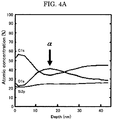
- the fixing member formed in the manner mentioned above is analyzed with XPS along with the depth direction thereof from the outermost layer to the inner portion thereof.
- XPS is a device capable of detecting an atom concentration of atoms of the measuring sample, or a bonding state thereof by capturing electrons jumped due to the photoelectron effect.
- a wide scan spectrum is measured with targeting the main components to Si, O, and C owing to the siloxane bond, and an atomic concentration ratio (atomic %) of each atom in the depth direction is measured based on a relative peak intensity ratio of each element present in an area from the surface layer to the inner portion.
- the results are depicted in FIG. 4A .
- the horizontal axis indicates the analysis depth from the surface towards the inner portion, and the longitudinal axis indicates the atomic ratio.
- atoms bonded to the silicon atom and the bonding state can be detected by measuring the energy at which electrons of 2p orbital of Si jump.
- the peak is separated from the narrow scan spectrum of the Si 2p orbital depicting the bonding state of Si as in FIG. 4B , the state of chemical bonds is analyzed.
- the horizontal axis indicates the bonding energy, and the longitudinal axis indicates the intensity ratio.
- the arrow showing the direction from the bottom to the up indicates the measurement spectrums in the depth direction.
- the oxygen concentration increases from the outermost layer to the inner portion to have the maximum value, and the carbon concentration decreases from the outermost layer to the inner portion to have the minimum value.
- the oxygen concentration decreases after reaching the maximum value, and the carbon concentration increases after reaching the minimum value.
- the atom concentration of each atom in the entire portion is appropriately identical to that of untreated rubber.
- the maximum value of the oxygen detected at ⁇ of FIG. 4A matches the phenomenon that the Si 2p bonding energy shifts to the higher energy side ( ⁇ of FIG. 4B ), which indicates that the increase in the oxygen concentration is related to the number of oxygen atoms bonded to Si.
- the fixing member of the present invention has the maximum value of the oxygen atom concentration in an area which is 5 nm to 50 ⁇ m in depth from the outermost surface thereof as measured by XPS depth profiling presented in Table 1. Moreover, at the depth where the maximum value of the oxygen atom concentration can be attained, the coefficient A of the following formula 1 is preferably 0.5 or more.
- A B + C / D
- a polyorganosiloxane layer containing polyorganosiloxane having a silicon atom bonded to three or four oxygen atoms is formed on a surface of the elastic layer on the base.
- a thickness of the polyorganosiloxane layer is appropriately selected depending on the intended purpose without any restriction, but it is preferably 0.01 ⁇ m to 5 ⁇ m, more preferably 0.01 ⁇ m to 1.0 ⁇ m. When the thickness thereof is greater than 5 ⁇ m, the hardness thereof increases so that the resulting fixing member may not correspond to the irregularities of the paper or toner. When the thickness thereof is thinner than 0.01 ⁇ m, a sufficient durability of the polyorganosiloxane layer may not be obtained.
- the outermost surface of the elastic layer may be appropriately modified, and for example, the outermost surface may be modified with a coupling agent, various monomers, a photosensitive functional group, a hydrophobic group, or a hydrophilic group.
- a fluorine-based polymer may be formed at the outermost surface of the elastic layer.
- the outermost surface is formed of an amorphous resin containing at least one functional group selected from the group consisting of a hydroxyl group, a silanol group, a carboxyl group, and a group capable of hydrolysis, and the amorphous resin of the outermost surface and the heat resistant rubber of the elastic layer are bonded via oxygen atoms.
- the amorphous resin is appropriately selected depending on the intended purpose without any restriction, and examples thereof include a resin having a perfluoropolyether in a principle chain thereof.
- the group capable of hydrolysis is not particularly limited, and examples thereof include: an alkoxy group such as a methoxy group, and an ethoxy group; and an alkoxysilane group such as a methoxysilane group, and an ethoxysilane group.
- the coupling agent is appropriately selected depending on the intended purpose without any restriction, and examples thereof include a metal alkoxide, and a solution containing a metal alkoxide.
- the metal alkoxide include, for example, a silicone alkoxide-based monomer represented by the following general formula (1), partially hydrolyzed polycondensate thereof having a polymerization degree of about 2 to about 10, a mixture thereof, and/or a solution containing the foregoing monomer or compounds and an organic solvent.
- R 1(4-n) Si(OR 2 ) n General Formula (1)
- R 1 and R 2 are each independently a C1-C10 linear or branched chain alkyl group, an alkyl polyether chain, or an aryl group or derivatives thereof, and n is an integer of 2 to 4.
- Specific examples of the compound represented by the general formula (1) include dimethyl dimethoxysilane, diethyl diethoxysilane, diethyl dimethoxysilane, diethyl diethoxysilane, diphenyl dimethoxysilane, diphenyl diethoxysilane, methyl trimethoxysilane, methyl triethoxysilane, tetramethoxysilane, tetraethoxysilane, and tetrapropoxysilane.
- ethoxysilane is particularly preferable in view of durability.
- R 1 may be a fluoroalkyl group, or may be a fluoroalkyl acrylate or perfluoropolyether bonded via oxygen.
- a perfluoropolyether group is particularly preferable in view of flexibility and durability.
- vinyl silane such as vinyltris(B-methoxyethoxy)silane, vinyltriethoxysilane, and vinyltrimethoxysilane
- acryl silane such as ⁇ -methacryloxypropyl trimethoxysilane
- epoxy silane such as ⁇ -(3,4-ethoxycyclohexyl)ethyl trimethoxysilane, ⁇ -glycidoxypropyl trimethoxysilane, and ⁇ -glycidoxypropylmethyl diethoxysilane
- amino silane such as N- ⁇ (aminoethyl)- ⁇ -aminopropyl trimethoxysilane, N- ⁇ -(aminoethyl)- ⁇ -aminopropylmethyl dimethoxysilane, ⁇ -aminopropyl triethoxysilane, and N-phenyl- ⁇ -aminopropyl trimethoxysilane.
- a monomer represented by the general formula (1) provided that the metal atom is changed from Si to Ti, Sn, Al, or Zr may be used independently or in combination.
- the treatment with a surface treating agent such as the coupling agent can be performed by impregnating (e.g., coating and dipping) a surface of the elastic material with the surface treating agent after performing the surface modification treatment (e.g., a plasma treatment, electron beam crosslinking, and UV ozone treatment) on the elastic material.
- the surface modification treatment e.g., a plasma treatment, electron beam crosslinking, and UV ozone treatment
- a modified layer having the maximum value of the oxygen atom concentration can be formed.
- the surface treating agent By impregnating the surface of the elastic material with a surface treating agent such as the coupling agent by coating or dipping, the surface treating agent penetrates into the base so that the polyorganosiloxane is presented with the concentration distribution.
- This distribution gives a distribution of the oxygen atom concentration contained in the polyorganosiloxane to have the maximum value in the area which is 5 nm to 50 ⁇ m in depth from the outermost surface.
- the fixing member of the present invention preferably has universal hardness HU of 0.5 N/mm 2 or lower with an indentation depth of 5 ⁇ m.
- the universal hardness HU can be obtained, for example, according to DIN50359, by gradually pressing an indenter against the fixing member using a micro hardness tester Win-HUD, and determining the universal hardness from the pressing load and contact area of the indenter at the time when the depth of the indentation reaches 5 ⁇ m.
- the fixing member has the outermost surface having flexibility and movable in the vertical direction, and corresponding to bumps formed of a toner or irregularities on transfer paper, and can secure sufficient elasticity for attaining high quality images corresponding to full color image formation.
- the aforementioned structure can realize the fixing member, in which durability of the outermost surface has been significantly improved, by giving sufficient strength owing to the hardness against the state (abrasion loads) where the stress is horizontally applied to the interface and the shear stress is applied onto the surface.
- a fixing device and electrophotographic image forming apparatus realizing both high image quality and high reliability, and stable fixing over a long period can be provided.
- a primer layer for silicone was formed as a base on a cylindrical support (polyimide) having a length of 320 mm, and thickness of 50 ⁇ m, and was dried. Thereafter, fluorosilicone rubber (X36-420U, manufactured by Shin-Etsu Chemical Co., Ltd.) was formed in the thickness of 200 ⁇ m on the base, and heated at 150°C for 10 minutes.
- fluorosilicone rubber X36-420U, manufactured by Shin-Etsu Chemical Co., Ltd.
- the formed fluorosilicone rubber was subjected to a plasma treatment under the following conditions.
- a 0.1% fluorosilicon compound (OPTOOL DSX, manufactured by Daikin Industries. Ltd.) solution in which the fluorosilicon compound had been diluted with perfluorohexane, was applied by dip coating at the withdrawal speed of 10 mm/min, and then was left in the environment having the temperature of 60°C and the relative humidity of 90% for 30 minutes or longer. Thereafter, the resultant was dried at 150°C for 10 minutes to thereby prepare a fixing member.
- OPTOOL DSX manufactured by Daikin Industries. Ltd.
- the fixing member produced in the aforementioned manner was mounted as a fixing belt in a fixing device of imagio MPC3000, manufactured by Ricoh Company Limited, and using this device a paper feed test was carried out by printing a toner solid image on 30,000 sheets of paper.
- a paper feed test was carried out by printing a toner solid image on 30,000 sheets of paper.
- multipaper super white available from Askul Co., Ltd.
- the results of the abrasion resistance and release properties were evaluated based on the criteria presented in Table 3. The evaluation results thereof are presented in Table 4.
- the universal hardness was measured according to DIN50359 by means of a micro hardness tester Win-HUD, by gradually pressing an indenter against the fixing member under the conditions presented in Table 2 until a predetermined indentation depth, and determining the universal hardness from the pressing load and contact area of the indenter at the time when the indentation depth reached 5 ⁇ m.
- a fixing member was produced in the same manner as in Example 1, provided that instead of the fluorosilicone rubber, silicone rubber (DY35-2083, manufactured by Toray Industries, Inc.) was coated in the thickness of 200 ⁇ m, heated at 150°C for 30 minutes, and subjected to secondary cure at 200°C for 4 hours.
- the produced fixing member was evaluated in the same manner as in Example 1.
- a fixing member was produced in the same manner as in Example 1, provided that instead of OPTOOL DSX, tetraethoxysilane (i.e., tetraethyl orthosilicate) (manufactured by Wako Pure Chemical Industries, Ltd.) was applied by dip coating.
- the produced fixing member was evaluated in the same manner as in Example 1.
- a fixing member was produced in the same manner as in Example 2, provided that instead of OPTOOL DSX, tetraethoxysilane (i.e., tetraethyl orthosilicate) (manufactured by Wako Pure Chemical Industries, Ltd.) was applied by dip coating.
- the produced fixing member was evaluated in the same manner as in Example 1.
- a fixing member was produced in the same manner as in Example 1, provided that as the plasma reaction gas, nitrogen was used instead of argon.
- the produced fixing member was evaluated in the same manner as in Example 1.
- a fixing member was produced in the same manner as in Example 1, provided that as the plasma reaction gas, nitrogen was used instead of oxygen.
- the produced fixing member was evaluated in the same manner as in Example 1.
- a fixing member was produced in the same manner as in Example 1, provided that the resultant from the plasma treatment was used as a final product, i.e. the fixing member.
- the produced fixing member was evaluated in the same manner as in Example 1.
- a fixing member was produced in the same manner as in Example 1, provided that instead of OPTOOL DSX, tetraethyl orthsilicate (manufactured by Wako Pure Chemical Industries, Ltd.) was applied by dip coating, and acrylic rubber (Nipol AR51, manufactured by Zeon Corporation) was used instead of the fluorosilicone rubber.
- the produced fixing member was evaluated in the same manner as in Example 1.
- a fixing member was produced in the same manner as in Example 8, provided that the acrylic rubber was replaced with butyl rubber (BR51, manufactured by JSR Corporation). The produced fixing member was evaluated in the same manner as in Example 1.
- a fixing member was produced in the same manner as in Example 8, provided that the acrylic rubber was replaced with ethylene propylene rubber (EP11, manufactured by JSR Corporation). The produced fixing member was evaluated in the same manner as in Example 1.
- a fixing member was produced in the same manner as in Example 1, provided that instead of OPTOOL DSX, an ethanol solution of 50% titanium isopropoxide (manufactured by Japan Pure Chemical Co., Ltd.) was applied by dip coating. The produced fixing member was evaluated in the same manner as in Example 1.
- a primer layer for silicone was formed as a base on a cylindrical support (polyimide) having a length of 320 mm, and thickness of 50 ⁇ m, and was dried. Thereafter, fluorosilicone rubber (X36-420U, manufactured by Shin-Etsu Chemical Co., Ltd.) was formed in the thickness of 200 ⁇ m on the base, and heated at 150°C for 10 minutes, to thereby prepare a fixing member. The produced fixing member was evaluated in the same manner as in Example 1.
- a fixing member was produced in the same manner as in Comparative Example 1, provided that instead of the fluorosilicone rubber, silicone rubber (DY35-2083, manufactured by Toray Industries, Inc.) was coated in the thickness of 200 ⁇ m, heated at 150°C for 30 minutes, and subjected to secondary cure at 200°C for 4 hours.
- the produced fixing member was evaluated in the same manner as in Example 1.
- Indenter Quadrangular pyramid diamond having a plane angle of 136° Initial load 0.02 mN Maximum load 400 mN Duration for increasing load 10 sec Indentation depth 5 ⁇ m Measuring temperature 25°C ⁇ 2°C Table 3 Evaluation Item Evaluation manner Acceptable rank Evaluation criteria Peak of oxygen atom concentration Existence of the maximum value of the oxygen atom concentration in the area that is 5 nm to 50 ⁇ m in depth from the outermost surface as detected by the XPS depth profiling specified in Table 1. Present Present or, Not present Peak sift Existence of the sift of the peak at Si 2p orbital to the higher energy side, as measured by the XPS depth profiling specified in Table 1.
- Example 1 In comparison to Comparative Examples 1 and 2, the fixing member of Example 1 reached the highest acceptable levels in the ranks in all of the evaluation items of the abrasion resistance, and the release properties, and the effect of the invention could be confirmed.
- the present invention can provide a fixing member, which has excellent abrasion resistance, and does not cause image failures due to abrasion over a long period, when it is used in an image forming apparatus. Moreover, the present invention can provide a fixing member having sufficiently preferable release properties for not causing image offset. As a result, a fixing device the duration and reliability of which has been improved can be provided. Because of this fixing device, an electrophotographic photocopier, facsimile, or laser printer having high durability and reliability can be achieved, and be used, which contributes to "reduction in environmental loads" or "improvement in customer satisfaction.”
- the fixing member of the present invention can achieve both high image quality and high reliability, and can achieve stable fixing over a long period, and thus is suitably used as a fixing member for electrophotographic photocopiers, facsimiles, and laser printers.
Landscapes
- Physics & Mathematics (AREA)
- General Physics & Mathematics (AREA)
- Fixing For Electrophotography (AREA)
Applications Claiming Priority (2)
| Application Number | Priority Date | Filing Date | Title |
|---|---|---|---|
| JP2011044663A JP5652611B2 (ja) | 2011-03-02 | 2011-03-02 | 定着部材、定着装置及び画像形成装置 |
| PCT/JP2012/055290 WO2012118166A1 (en) | 2011-03-02 | 2012-02-24 | Fixing member, fixing device, and image forming apparatus |
Publications (3)
| Publication Number | Publication Date |
|---|---|
| EP2681630A1 EP2681630A1 (en) | 2014-01-08 |
| EP2681630A4 EP2681630A4 (en) | 2014-08-13 |
| EP2681630B1 true EP2681630B1 (en) | 2017-12-13 |
Family
ID=46758092
Family Applications (1)
| Application Number | Title | Priority Date | Filing Date |
|---|---|---|---|
| EP12752150.8A Not-in-force EP2681630B1 (en) | 2011-03-02 | 2012-02-24 | Fixing member, fixing device, and image forming apparatus |
Country Status (7)
| Country | Link |
|---|---|
| US (1) | US9037064B2 (enExample) |
| EP (1) | EP2681630B1 (enExample) |
| JP (1) | JP5652611B2 (enExample) |
| KR (1) | KR101501866B1 (enExample) |
| CN (1) | CN103415815B (enExample) |
| CA (1) | CA2828502C (enExample) |
| WO (1) | WO2012118166A1 (enExample) |
Families Citing this family (8)
| Publication number | Priority date | Publication date | Assignee | Title |
|---|---|---|---|---|
| JP2014102491A (ja) * | 2012-10-26 | 2014-06-05 | Ricoh Co Ltd | 定着部材、定着装置及び画像形成装置 |
| JP6146697B2 (ja) * | 2013-06-20 | 2017-06-14 | 株式会社リコー | 定着部材、定着装置及び画像形成装置 |
| JP2015148760A (ja) * | 2014-02-07 | 2015-08-20 | コニカミノルタ株式会社 | 定着ベルト、定着装置および画像形成装置 |
| JP6870200B2 (ja) | 2014-11-13 | 2021-05-12 | 株式会社リコー | 素子、及び発電装置 |
| US11010004B2 (en) * | 2016-03-14 | 2021-05-18 | Ricoh Company, Ltd. | Input element and input device |
| JP6808979B2 (ja) * | 2016-06-01 | 2021-01-06 | 株式会社リコー | 入力素子及び入力装置 |
| JP2020515697A (ja) * | 2017-04-03 | 2020-05-28 | ソルベイ スペシャルティ ポリマーズ イタリー エス.ピー.エー. | 作動流体組成物 |
| WO2021076146A1 (en) * | 2019-10-18 | 2021-04-22 | Hewlett-Packard Development Company, L.P. | Marking photoconductors of print apparatuses |
Family Cites Families (48)
| Publication number | Priority date | Publication date | Assignee | Title |
|---|---|---|---|---|
| JPS523305B2 (enExample) | 1972-10-23 | 1977-01-27 | ||
| JPS523304B2 (enExample) | 1972-10-21 | 1977-01-27 | ||
| US4301355A (en) | 1980-08-04 | 1981-11-17 | Dimetrics, Inc. | Gas metal arc welding system |
| JPH01306472A (ja) * | 1988-06-06 | 1989-12-11 | Canon Inc | シリコーンゴム組成物、該組成物から形成される成形物、該組成物を有する弾性回転体及び定着装置 |
| US4970559A (en) * | 1987-11-10 | 1990-11-13 | Canon Kabushiki Kaisha | Organic polymer material having antistatic property, elastic revolution body and fixing device using the same |
| NL8801669A (nl) | 1988-07-01 | 1990-02-01 | Oce Nederland Bv | Inrichting voor het fixeren of transfereren en fixeren van thermoplastische hars bevattend poeder op een ontvangstmateriaal. |
| JPH03243991A (ja) | 1990-02-22 | 1991-10-30 | Nec Corp | データ表示装置 |
| JP2949243B2 (ja) | 1990-10-15 | 1999-09-13 | 辰栄工業株式会社 | マスターシリンダ |
| US5327202A (en) * | 1991-08-01 | 1994-07-05 | Canon Kabushiki Kaisha | Elastic body of an addition reaction type silicone rubber elastic material used in elastic roller and fixing device |
| JPH0566589A (ja) | 1991-09-09 | 1993-03-19 | Dainippon Ink & Chem Inc | 電子写真感光体 |
| JPH07311508A (ja) | 1994-03-25 | 1995-11-28 | Canon Inc | 定着用ローラ及び定着装置 |
| US5608508A (en) * | 1994-03-25 | 1997-03-04 | Canon Kabushiki Kaisha | Rotatable member for fixing in which inorganic filler is contained in silicone rubber, and fixing device having the same |
| JPH0811243A (ja) * | 1994-06-30 | 1996-01-16 | Toray Dow Corning Silicone Co Ltd | 定着ロールの製造方法 |
| JP3603428B2 (ja) | 1995-07-17 | 2004-12-22 | 大日本インキ化学工業株式会社 | 成分濃度傾斜構造を有する有機高分子と金属酸化物との複合体の製造方法 |
| US5679463A (en) * | 1995-07-31 | 1997-10-21 | Eastman Kodak Company | Condensation-cured PDMS filled with zinc oxide and tin oxide mixed fillers for improved fusing member materials |
| JP3153454B2 (ja) * | 1995-11-10 | 2001-04-09 | 東レ・ダウコーニング・シリコーン株式会社 | 定着ロールおよびそのためのシリコーンゲル組成物 |
| JP3243991B2 (ja) | 1995-12-18 | 2002-01-07 | 信越化学工業株式会社 | 定着ロール用付加型加熱硬化性シリコーンエラストマー組成物及びその製造方法 |
| JP3216799B2 (ja) * | 1996-11-13 | 2001-10-09 | 松下電工株式会社 | 加熱定着ロール |
| JP2000112271A (ja) | 1998-10-01 | 2000-04-21 | Fuji Xerox Co Ltd | 定着用部材とその製造方法及びそれを用いた定着装置 |
| JP2000267487A (ja) * | 1999-03-19 | 2000-09-29 | Fuji Xerox Co Ltd | 定着用弾性回転体の製造方法 |
| JP4045726B2 (ja) * | 2000-08-03 | 2008-02-13 | 東海ゴム工業株式会社 | Oa機器用ローラ |
| JP2002082558A (ja) | 2000-09-08 | 2002-03-22 | Ricoh Co Ltd | 定着部材及びそれを有する画像形成装置 |
| JP2004077886A (ja) | 2002-08-20 | 2004-03-11 | Ricoh Co Ltd | 定着部材及びその製造方法並びにそれを有する画像形成装置 |
| JP4151359B2 (ja) | 2002-09-13 | 2008-09-17 | 富士ゼロックス株式会社 | 定着部材、及びそれを用いた画像形成装置 |
| JP4334842B2 (ja) * | 2002-10-02 | 2009-09-30 | 信越化学工業株式会社 | 定着ロールの圧縮永久歪を低減する方法、及び定着ロール |
| JP2004252000A (ja) | 2003-02-18 | 2004-09-09 | Suzuka Fuji Xerox Co Ltd | 電子写真用弾性材料 |
| JP2004279590A (ja) | 2003-03-13 | 2004-10-07 | Ricoh Co Ltd | 定着部材及びそれを有する画像形成装置 |
| US6838140B1 (en) * | 2003-06-13 | 2005-01-04 | Xerox Corporation | Fuser member having platinum catalyzed addition cured silicone layer |
| JP4351498B2 (ja) * | 2003-08-11 | 2009-10-28 | 株式会社リコー | 定着用弾性回転体及びその製造方法並びにそれを有する画像形成装置 |
| JP4250043B2 (ja) * | 2003-09-08 | 2009-04-08 | 株式会社リコー | 定着用弾性回転体及びそれを有する画像形成装置 |
| US7029966B2 (en) | 2003-09-18 | 2006-04-18 | International Business Machines Corporation | Process options of forming silicided metal gates for advanced CMOS devices |
| JP4262038B2 (ja) * | 2003-09-19 | 2009-05-13 | キヤノン株式会社 | チューブ被覆ベルト及びその製造方法、並びに加熱定着装置 |
| JP4653452B2 (ja) | 2003-10-24 | 2011-03-16 | 株式会社リコー | 定着部材、定着装置、及び画像形成装置 |
| JP4312669B2 (ja) | 2004-03-19 | 2009-08-12 | 株式会社リコー | 定着部材、該定着部材を用いた定着装置および画像形成装置 |
| JP2006133624A (ja) | 2004-11-09 | 2006-05-25 | Ricoh Co Ltd | 定着装置、画像形成装置 |
| JP2006176293A (ja) | 2004-12-22 | 2006-07-06 | Kyocera Mita Corp | 画像形成装置 |
| JP2006235421A (ja) | 2005-02-28 | 2006-09-07 | Ricoh Co Ltd | 転写定着装置、それに用いる転写定着部材、及び、それを有する画像形成装置 |
| JP4827080B2 (ja) | 2005-12-19 | 2011-11-30 | 株式会社リコー | 定着装置及び画像形成装置 |
| JP4490474B2 (ja) * | 2006-12-21 | 2010-06-23 | キヤノン株式会社 | 電子写真用定着部材、定着装置および電子写真画像形成装置 |
| WO2008078582A1 (ja) | 2006-12-22 | 2008-07-03 | Canon Kabushiki Kaisha | 定着部材、その製造方法、それを用いた定着装置及び電子写真画像形成装置 |
| JP4378406B2 (ja) * | 2006-12-22 | 2009-12-09 | キヤノン株式会社 | 定着部材、その製造方法、それを用いた定着装置及び電子写真画像形成装置 |
| JP5279195B2 (ja) * | 2007-04-09 | 2013-09-04 | 信越化学工業株式会社 | 定着ロール又は定着ベルト用シリコーンゴム組成物、並びに定着ロール及び定着ベルト |
| JP4948290B2 (ja) | 2007-06-29 | 2012-06-06 | 株式会社リコー | 定着装置 |
| JP5282292B2 (ja) | 2007-07-30 | 2013-09-04 | コニカミノルタ株式会社 | ローラ、ベルト定着装置及び画像形成装置 |
| JP4795379B2 (ja) | 2008-04-10 | 2011-10-19 | 株式会社リコー | 定着液、定着方法、定着装置、画像形成方法及び画像形成装置 |
| JP5152650B2 (ja) | 2008-04-22 | 2013-02-27 | 株式会社リコー | 画質改善処理液、画質改善処理方法、画像形成方法及び画像形成装置 |
| JP5439993B2 (ja) * | 2008-11-13 | 2014-03-12 | 株式会社リコー | 定着部材及びその製造方法、並びに定着装置及び画像形成装置 |
| JP5740803B2 (ja) | 2008-11-21 | 2015-07-01 | 株式会社リコー | 定着部材、並びにこれを備えた定着装置及び画像形成装置 |
-
2011
- 2011-03-02 JP JP2011044663A patent/JP5652611B2/ja not_active Expired - Fee Related
-
2012
- 2012-02-24 CN CN201280010936.1A patent/CN103415815B/zh not_active Expired - Fee Related
- 2012-02-24 CA CA2828502A patent/CA2828502C/en not_active Expired - Fee Related
- 2012-02-24 US US13/984,388 patent/US9037064B2/en not_active Expired - Fee Related
- 2012-02-24 KR KR1020137025569A patent/KR101501866B1/ko not_active Expired - Fee Related
- 2012-02-24 WO PCT/JP2012/055290 patent/WO2012118166A1/en not_active Ceased
- 2012-02-24 EP EP12752150.8A patent/EP2681630B1/en not_active Not-in-force
Non-Patent Citations (1)
| Title |
|---|
| None * |
Also Published As
| Publication number | Publication date |
|---|---|
| KR20130133856A (ko) | 2013-12-09 |
| US20130322942A1 (en) | 2013-12-05 |
| CA2828502A1 (en) | 2012-09-07 |
| EP2681630A1 (en) | 2014-01-08 |
| EP2681630A4 (en) | 2014-08-13 |
| US9037064B2 (en) | 2015-05-19 |
| JP5652611B2 (ja) | 2015-01-14 |
| CN103415815B (zh) | 2016-03-16 |
| CN103415815A (zh) | 2013-11-27 |
| WO2012118166A1 (en) | 2012-09-07 |
| CA2828502C (en) | 2016-04-05 |
| JP2012181381A (ja) | 2012-09-20 |
| KR101501866B1 (ko) | 2015-03-11 |
Similar Documents
| Publication | Publication Date | Title |
|---|---|---|
| EP2681630B1 (en) | Fixing member, fixing device, and image forming apparatus | |
| JP7467725B2 (ja) | 定着部材の製造方法 | |
| US7991341B2 (en) | Electrophotographic fixing member and manufacturing method thereof, fixing apparatus, and electrophotographic image forming apparatus | |
| CN101395541B (zh) | 充电构件、处理盒和电子照相设备 | |
| JP7587357B2 (ja) | 定着部材、定着装置及び画像形成装置 | |
| JP4948666B2 (ja) | 帯電部材及びその製造方法 | |
| EP3731024B1 (en) | Fixing member and heat fixing device | |
| US20120322967A1 (en) | Fixing member, fixing device, and image forming apparatus | |
| US9411281B2 (en) | Fixing member, fixing device, and image forming apparatus | |
| KR20130079549A (ko) | 대전 부재, 프로세스 카트리지 및 전자 사진 장치 | |
| US20220334522A1 (en) | Fixing member and heat fixing apparatus | |
| JP7631107B2 (ja) | 定着部材及び熱定着装置 | |
| JP5862934B2 (ja) | 定着部材、それを用いた定着装置および画像形成装置 | |
| JP7822838B2 (ja) | 定着部材及び熱定着装置 | |
| JP5137170B2 (ja) | 半導電性ローラの製造方法 | |
| JP2025018226A (ja) | 電子写真部材、加熱定着装置及び電子写真画像形成装置 | |
| JP2003241537A (ja) | 電子写真装置用転写定着部材 |
Legal Events
| Date | Code | Title | Description |
|---|---|---|---|
| PUAI | Public reference made under article 153(3) epc to a published international application that has entered the european phase |
Free format text: ORIGINAL CODE: 0009012 |
|
| 17P | Request for examination filed |
Effective date: 20130815 |
|
| AK | Designated contracting states |
Kind code of ref document: A1 Designated state(s): AL AT BE BG CH CY CZ DE DK EE ES FI FR GB GR HR HU IE IS IT LI LT LU LV MC MK MT NL NO PL PT RO RS SE SI SK SM TR |
|
| DAX | Request for extension of the european patent (deleted) | ||
| A4 | Supplementary search report drawn up and despatched |
Effective date: 20140716 |
|
| RIC1 | Information provided on ipc code assigned before grant |
Ipc: G03G 15/20 20060101AFI20140710BHEP |
|
| GRAP | Despatch of communication of intention to grant a patent |
Free format text: ORIGINAL CODE: EPIDOSNIGR1 |
|
| INTG | Intention to grant announced |
Effective date: 20170623 |
|
| GRAS | Grant fee paid |
Free format text: ORIGINAL CODE: EPIDOSNIGR3 |
|
| GRAA | (expected) grant |
Free format text: ORIGINAL CODE: 0009210 |
|
| AK | Designated contracting states |
Kind code of ref document: B1 Designated state(s): AL AT BE BG CH CY CZ DE DK EE ES FI FR GB GR HR HU IE IS IT LI LT LU LV MC MK MT NL NO PL PT RO RS SE SI SK SM TR |
|
| REG | Reference to a national code |
Ref country code: GB Ref legal event code: FG4D |
|
| RIN1 | Information on inventor provided before grant (corrected) |
Inventor name: KONDOH, TSUNEAKI Inventor name: SUGAWARA, TOMOAKI Inventor name: NATORI, JUNICHIRO |
|
| REG | Reference to a national code |
Ref country code: AT Ref legal event code: REF Ref document number: 954971 Country of ref document: AT Kind code of ref document: T Effective date: 20171215 Ref country code: CH Ref legal event code: EP |
|
| REG | Reference to a national code |
Ref country code: IE Ref legal event code: FG4D |
|
| REG | Reference to a national code |
Ref country code: DE Ref legal event code: R096 Ref document number: 602012040845 Country of ref document: DE |
|
| REG | Reference to a national code |
Ref country code: FR Ref legal event code: PLFP Year of fee payment: 7 |
|
| REG | Reference to a national code |
Ref country code: NL Ref legal event code: MP Effective date: 20171213 |
|
| REG | Reference to a national code |
Ref country code: LT Ref legal event code: MG4D |
|
| PG25 | Lapsed in a contracting state [announced via postgrant information from national office to epo] |
Ref country code: FI Free format text: LAPSE BECAUSE OF FAILURE TO SUBMIT A TRANSLATION OF THE DESCRIPTION OR TO PAY THE FEE WITHIN THE PRESCRIBED TIME-LIMIT Effective date: 20171213 Ref country code: NO Free format text: LAPSE BECAUSE OF FAILURE TO SUBMIT A TRANSLATION OF THE DESCRIPTION OR TO PAY THE FEE WITHIN THE PRESCRIBED TIME-LIMIT Effective date: 20180313 Ref country code: SE Free format text: LAPSE BECAUSE OF FAILURE TO SUBMIT A TRANSLATION OF THE DESCRIPTION OR TO PAY THE FEE WITHIN THE PRESCRIBED TIME-LIMIT Effective date: 20171213 Ref country code: LT Free format text: LAPSE BECAUSE OF FAILURE TO SUBMIT A TRANSLATION OF THE DESCRIPTION OR TO PAY THE FEE WITHIN THE PRESCRIBED TIME-LIMIT Effective date: 20171213 |
|
| REG | Reference to a national code |
Ref country code: AT Ref legal event code: MK05 Ref document number: 954971 Country of ref document: AT Kind code of ref document: T Effective date: 20171213 |
|
| PG25 | Lapsed in a contracting state [announced via postgrant information from national office to epo] |
Ref country code: RS Free format text: LAPSE BECAUSE OF FAILURE TO SUBMIT A TRANSLATION OF THE DESCRIPTION OR TO PAY THE FEE WITHIN THE PRESCRIBED TIME-LIMIT Effective date: 20171213 Ref country code: BG Free format text: LAPSE BECAUSE OF FAILURE TO SUBMIT A TRANSLATION OF THE DESCRIPTION OR TO PAY THE FEE WITHIN THE PRESCRIBED TIME-LIMIT Effective date: 20180313 Ref country code: HR Free format text: LAPSE BECAUSE OF FAILURE TO SUBMIT A TRANSLATION OF THE DESCRIPTION OR TO PAY THE FEE WITHIN THE PRESCRIBED TIME-LIMIT Effective date: 20171213 Ref country code: GR Free format text: LAPSE BECAUSE OF FAILURE TO SUBMIT A TRANSLATION OF THE DESCRIPTION OR TO PAY THE FEE WITHIN THE PRESCRIBED TIME-LIMIT Effective date: 20180314 Ref country code: LV Free format text: LAPSE BECAUSE OF FAILURE TO SUBMIT A TRANSLATION OF THE DESCRIPTION OR TO PAY THE FEE WITHIN THE PRESCRIBED TIME-LIMIT Effective date: 20171213 |
|
| PG25 | Lapsed in a contracting state [announced via postgrant information from national office to epo] |
Ref country code: NL Free format text: LAPSE BECAUSE OF FAILURE TO SUBMIT A TRANSLATION OF THE DESCRIPTION OR TO PAY THE FEE WITHIN THE PRESCRIBED TIME-LIMIT Effective date: 20171213 |
|
| PG25 | Lapsed in a contracting state [announced via postgrant information from national office to epo] |
Ref country code: EE Free format text: LAPSE BECAUSE OF FAILURE TO SUBMIT A TRANSLATION OF THE DESCRIPTION OR TO PAY THE FEE WITHIN THE PRESCRIBED TIME-LIMIT Effective date: 20171213 Ref country code: CY Free format text: LAPSE BECAUSE OF FAILURE TO SUBMIT A TRANSLATION OF THE DESCRIPTION OR TO PAY THE FEE WITHIN THE PRESCRIBED TIME-LIMIT Effective date: 20171213 Ref country code: SK Free format text: LAPSE BECAUSE OF FAILURE TO SUBMIT A TRANSLATION OF THE DESCRIPTION OR TO PAY THE FEE WITHIN THE PRESCRIBED TIME-LIMIT Effective date: 20171213 Ref country code: ES Free format text: LAPSE BECAUSE OF FAILURE TO SUBMIT A TRANSLATION OF THE DESCRIPTION OR TO PAY THE FEE WITHIN THE PRESCRIBED TIME-LIMIT Effective date: 20171213 Ref country code: CZ Free format text: LAPSE BECAUSE OF FAILURE TO SUBMIT A TRANSLATION OF THE DESCRIPTION OR TO PAY THE FEE WITHIN THE PRESCRIBED TIME-LIMIT Effective date: 20171213 |
|
| PG25 | Lapsed in a contracting state [announced via postgrant information from national office to epo] |
Ref country code: PL Free format text: LAPSE BECAUSE OF FAILURE TO SUBMIT A TRANSLATION OF THE DESCRIPTION OR TO PAY THE FEE WITHIN THE PRESCRIBED TIME-LIMIT Effective date: 20171213 Ref country code: RO Free format text: LAPSE BECAUSE OF FAILURE TO SUBMIT A TRANSLATION OF THE DESCRIPTION OR TO PAY THE FEE WITHIN THE PRESCRIBED TIME-LIMIT Effective date: 20171213 Ref country code: IS Free format text: LAPSE BECAUSE OF FAILURE TO SUBMIT A TRANSLATION OF THE DESCRIPTION OR TO PAY THE FEE WITHIN THE PRESCRIBED TIME-LIMIT Effective date: 20180413 Ref country code: SM Free format text: LAPSE BECAUSE OF FAILURE TO SUBMIT A TRANSLATION OF THE DESCRIPTION OR TO PAY THE FEE WITHIN THE PRESCRIBED TIME-LIMIT Effective date: 20171213 Ref country code: AT Free format text: LAPSE BECAUSE OF FAILURE TO SUBMIT A TRANSLATION OF THE DESCRIPTION OR TO PAY THE FEE WITHIN THE PRESCRIBED TIME-LIMIT Effective date: 20171213 Ref country code: IT Free format text: LAPSE BECAUSE OF FAILURE TO SUBMIT A TRANSLATION OF THE DESCRIPTION OR TO PAY THE FEE WITHIN THE PRESCRIBED TIME-LIMIT Effective date: 20171213 |
|
| REG | Reference to a national code |
Ref country code: CH Ref legal event code: PL Ref country code: DE Ref legal event code: R097 Ref document number: 602012040845 Country of ref document: DE |
|
| PG25 | Lapsed in a contracting state [announced via postgrant information from national office to epo] |
Ref country code: MC Free format text: LAPSE BECAUSE OF FAILURE TO SUBMIT A TRANSLATION OF THE DESCRIPTION OR TO PAY THE FEE WITHIN THE PRESCRIBED TIME-LIMIT Effective date: 20171213 |
|
| PLBE | No opposition filed within time limit |
Free format text: ORIGINAL CODE: 0009261 |
|
| STAA | Information on the status of an ep patent application or granted ep patent |
Free format text: STATUS: NO OPPOSITION FILED WITHIN TIME LIMIT |
|
| 26N | No opposition filed |
Effective date: 20180914 |
|
| REG | Reference to a national code |
Ref country code: IE Ref legal event code: MM4A |
|
| REG | Reference to a national code |
Ref country code: BE Ref legal event code: MM Effective date: 20180228 |
|
| PG25 | Lapsed in a contracting state [announced via postgrant information from national office to epo] |
Ref country code: DK Free format text: LAPSE BECAUSE OF FAILURE TO SUBMIT A TRANSLATION OF THE DESCRIPTION OR TO PAY THE FEE WITHIN THE PRESCRIBED TIME-LIMIT Effective date: 20171213 Ref country code: LU Free format text: LAPSE BECAUSE OF NON-PAYMENT OF DUE FEES Effective date: 20180224 Ref country code: LI Free format text: LAPSE BECAUSE OF NON-PAYMENT OF DUE FEES Effective date: 20180228 Ref country code: CH Free format text: LAPSE BECAUSE OF NON-PAYMENT OF DUE FEES Effective date: 20180228 |
|
| PG25 | Lapsed in a contracting state [announced via postgrant information from national office to epo] |
Ref country code: IE Free format text: LAPSE BECAUSE OF NON-PAYMENT OF DUE FEES Effective date: 20180224 |
|
| PG25 | Lapsed in a contracting state [announced via postgrant information from national office to epo] |
Ref country code: SI Free format text: LAPSE BECAUSE OF FAILURE TO SUBMIT A TRANSLATION OF THE DESCRIPTION OR TO PAY THE FEE WITHIN THE PRESCRIBED TIME-LIMIT Effective date: 20171213 Ref country code: BE Free format text: LAPSE BECAUSE OF NON-PAYMENT OF DUE FEES Effective date: 20180228 |
|
| PG25 | Lapsed in a contracting state [announced via postgrant information from national office to epo] |
Ref country code: MT Free format text: LAPSE BECAUSE OF NON-PAYMENT OF DUE FEES Effective date: 20180224 |
|
| PG25 | Lapsed in a contracting state [announced via postgrant information from national office to epo] |
Ref country code: TR Free format text: LAPSE BECAUSE OF FAILURE TO SUBMIT A TRANSLATION OF THE DESCRIPTION OR TO PAY THE FEE WITHIN THE PRESCRIBED TIME-LIMIT Effective date: 20171213 |
|
| PGFP | Annual fee paid to national office [announced via postgrant information from national office to epo] |
Ref country code: DE Payment date: 20200219 Year of fee payment: 9 Ref country code: GB Payment date: 20200219 Year of fee payment: 9 |
|
| PG25 | Lapsed in a contracting state [announced via postgrant information from national office to epo] |
Ref country code: HU Free format text: LAPSE BECAUSE OF FAILURE TO SUBMIT A TRANSLATION OF THE DESCRIPTION OR TO PAY THE FEE WITHIN THE PRESCRIBED TIME-LIMIT; INVALID AB INITIO Effective date: 20120224 Ref country code: PT Free format text: LAPSE BECAUSE OF FAILURE TO SUBMIT A TRANSLATION OF THE DESCRIPTION OR TO PAY THE FEE WITHIN THE PRESCRIBED TIME-LIMIT Effective date: 20171213 |
|
| PG25 | Lapsed in a contracting state [announced via postgrant information from national office to epo] |
Ref country code: MK Free format text: LAPSE BECAUSE OF NON-PAYMENT OF DUE FEES Effective date: 20171213 |
|
| PGFP | Annual fee paid to national office [announced via postgrant information from national office to epo] |
Ref country code: FR Payment date: 20200219 Year of fee payment: 9 |
|
| PG25 | Lapsed in a contracting state [announced via postgrant information from national office to epo] |
Ref country code: AL Free format text: LAPSE BECAUSE OF FAILURE TO SUBMIT A TRANSLATION OF THE DESCRIPTION OR TO PAY THE FEE WITHIN THE PRESCRIBED TIME-LIMIT Effective date: 20171213 |
|
| REG | Reference to a national code |
Ref country code: DE Ref legal event code: R119 Ref document number: 602012040845 Country of ref document: DE |
|
| GBPC | Gb: european patent ceased through non-payment of renewal fee |
Effective date: 20210224 |
|
| PG25 | Lapsed in a contracting state [announced via postgrant information from national office to epo] |
Ref country code: FR Free format text: LAPSE BECAUSE OF NON-PAYMENT OF DUE FEES Effective date: 20210228 Ref country code: GB Free format text: LAPSE BECAUSE OF NON-PAYMENT OF DUE FEES Effective date: 20210224 Ref country code: DE Free format text: LAPSE BECAUSE OF NON-PAYMENT OF DUE FEES Effective date: 20210901 |