EP2650923B1 - Cellule solaire, module cellule solaire et methode de fabrication de cellule solaire - Google Patents
Cellule solaire, module cellule solaire et methode de fabrication de cellule solaire Download PDFInfo
- Publication number
- EP2650923B1 EP2650923B1 EP11846590.5A EP11846590A EP2650923B1 EP 2650923 B1 EP2650923 B1 EP 2650923B1 EP 11846590 A EP11846590 A EP 11846590A EP 2650923 B1 EP2650923 B1 EP 2650923B1
- Authority
- EP
- European Patent Office
- Prior art keywords
- electrode
- back side
- solar cell
- conductive paste
- dopant
- Prior art date
- Legal status (The legal status is an assumption and is not a legal conclusion. Google has not performed a legal analysis and makes no representation as to the accuracy of the status listed.)
- Active
Links
- 238000004519 manufacturing process Methods 0.000 title claims description 12
- 229910052710 silicon Inorganic materials 0.000 claims description 59
- 239000000758 substrate Substances 0.000 claims description 59
- XUIMIQQOPSSXEZ-UHFFFAOYSA-N Silicon Chemical compound [Si] XUIMIQQOPSSXEZ-UHFFFAOYSA-N 0.000 claims description 57
- 239000010703 silicon Substances 0.000 claims description 56
- 239000010410 layer Substances 0.000 claims description 54
- 239000002019 doping agent Substances 0.000 claims description 38
- 238000000605 extraction Methods 0.000 claims description 38
- 238000002161 passivation Methods 0.000 claims description 28
- 238000000034 method Methods 0.000 claims description 27
- 238000010304 firing Methods 0.000 claims description 25
- BQCADISMDOOEFD-UHFFFAOYSA-N Silver Chemical compound [Ag] BQCADISMDOOEFD-UHFFFAOYSA-N 0.000 claims description 23
- 239000011521 glass Substances 0.000 claims description 11
- 229910052581 Si3N4 Inorganic materials 0.000 claims description 9
- HQVNEWCFYHHQES-UHFFFAOYSA-N silicon nitride Chemical compound N12[Si]34N5[Si]62N3[Si]51N64 HQVNEWCFYHHQES-UHFFFAOYSA-N 0.000 claims description 9
- 238000010438 heat treatment Methods 0.000 claims description 8
- 229910052698 phosphorus Inorganic materials 0.000 claims description 8
- 238000007650 screen-printing Methods 0.000 claims description 8
- 239000002356 single layer Substances 0.000 claims description 8
- 229910021419 crystalline silicon Inorganic materials 0.000 claims description 7
- 239000002003 electrode paste Substances 0.000 claims description 7
- 229910052782 aluminium Inorganic materials 0.000 claims description 6
- 229910052787 antimony Inorganic materials 0.000 claims description 5
- 229910052796 boron Inorganic materials 0.000 claims description 5
- 229910052733 gallium Inorganic materials 0.000 claims description 5
- 150000001875 compounds Chemical class 0.000 claims description 4
- VYPSYNLAJGMNEJ-UHFFFAOYSA-N Silicium dioxide Chemical compound O=[Si]=O VYPSYNLAJGMNEJ-UHFFFAOYSA-N 0.000 claims description 3
- 229910052738 indium Inorganic materials 0.000 claims description 3
- 229910052814 silicon oxide Inorganic materials 0.000 claims description 3
- GWEVSGVZZGPLCZ-UHFFFAOYSA-N Titan oxide Chemical compound O=[Ti]=O GWEVSGVZZGPLCZ-UHFFFAOYSA-N 0.000 claims description 2
- 229910021417 amorphous silicon Inorganic materials 0.000 claims description 2
- 229910052785 arsenic Inorganic materials 0.000 claims description 2
- 229910021424 microcrystalline silicon Inorganic materials 0.000 claims description 2
- TWNQGVIAIRXVLR-UHFFFAOYSA-N oxo(oxoalumanyloxy)alumane Chemical compound O=[Al]O[Al]=O TWNQGVIAIRXVLR-UHFFFAOYSA-N 0.000 claims description 2
- HBMJWWWQQXIZIP-UHFFFAOYSA-N silicon carbide Chemical compound [Si+]#[C-] HBMJWWWQQXIZIP-UHFFFAOYSA-N 0.000 claims description 2
- 229910010271 silicon carbide Inorganic materials 0.000 claims description 2
- OGIDPMRJRNCKJF-UHFFFAOYSA-N titanium oxide Inorganic materials [Ti]=O OGIDPMRJRNCKJF-UHFFFAOYSA-N 0.000 claims description 2
- 238000005245 sintering Methods 0.000 claims 11
- 230000000149 penetrating effect Effects 0.000 claims 2
- 229910052709 silver Inorganic materials 0.000 description 18
- 239000004332 silver Substances 0.000 description 14
- KWYUFKZDYYNOTN-UHFFFAOYSA-M Potassium hydroxide Chemical compound [OH-].[K+] KWYUFKZDYYNOTN-UHFFFAOYSA-M 0.000 description 12
- 238000009792 diffusion process Methods 0.000 description 11
- 238000007639 printing Methods 0.000 description 11
- 239000000523 sample Substances 0.000 description 10
- 230000005684 electric field Effects 0.000 description 9
- KRHYYFGTRYWZRS-UHFFFAOYSA-N Fluorane Chemical compound F KRHYYFGTRYWZRS-UHFFFAOYSA-N 0.000 description 8
- VEXZGXHMUGYJMC-UHFFFAOYSA-N Hydrochloric acid Chemical compound Cl VEXZGXHMUGYJMC-UHFFFAOYSA-N 0.000 description 8
- KFZMGEQAYNKOFK-UHFFFAOYSA-N Isopropanol Chemical compound CC(C)O KFZMGEQAYNKOFK-UHFFFAOYSA-N 0.000 description 6
- HEMHJVSKTPXQMS-UHFFFAOYSA-M Sodium hydroxide Chemical compound [OH-].[Na+] HEMHJVSKTPXQMS-UHFFFAOYSA-M 0.000 description 6
- 229910052751 metal Inorganic materials 0.000 description 6
- 239000002184 metal Substances 0.000 description 6
- XHXFXVLFKHQFAL-UHFFFAOYSA-N phosphoryl trichloride Chemical compound ClP(Cl)(Cl)=O XHXFXVLFKHQFAL-UHFFFAOYSA-N 0.000 description 6
- 239000011230 binding agent Substances 0.000 description 5
- 238000005229 chemical vapour deposition Methods 0.000 description 5
- 230000000052 comparative effect Effects 0.000 description 5
- 230000000694 effects Effects 0.000 description 5
- 238000005215 recombination Methods 0.000 description 5
- 230000006798 recombination Effects 0.000 description 5
- 239000012808 vapor phase Substances 0.000 description 5
- QGZKDVFQNNGYKY-UHFFFAOYSA-N Ammonia Chemical compound N QGZKDVFQNNGYKY-UHFFFAOYSA-N 0.000 description 4
- MHAJPDPJQMAIIY-UHFFFAOYSA-N Hydrogen peroxide Chemical compound OO MHAJPDPJQMAIIY-UHFFFAOYSA-N 0.000 description 4
- XAGFODPZIPBFFR-UHFFFAOYSA-N aluminium Chemical compound [Al] XAGFODPZIPBFFR-UHFFFAOYSA-N 0.000 description 4
- 230000008901 benefit Effects 0.000 description 4
- 230000015572 biosynthetic process Effects 0.000 description 4
- 229910021478 group 5 element Inorganic materials 0.000 description 4
- 238000005259 measurement Methods 0.000 description 4
- 239000000203 mixture Substances 0.000 description 4
- 230000003287 optical effect Effects 0.000 description 4
- 238000005406 washing Methods 0.000 description 4
- 238000010521 absorption reaction Methods 0.000 description 3
- 239000012670 alkaline solution Substances 0.000 description 3
- 239000000969 carrier Substances 0.000 description 3
- 239000007789 gas Substances 0.000 description 3
- 238000002156 mixing Methods 0.000 description 3
- 229910021421 monocrystalline silicon Inorganic materials 0.000 description 3
- 239000011574 phosphorus Substances 0.000 description 3
- IJGRMHOSHXDMSA-UHFFFAOYSA-N Atomic nitrogen Chemical compound N#N IJGRMHOSHXDMSA-UHFFFAOYSA-N 0.000 description 2
- GRYLNZFGIOXLOG-UHFFFAOYSA-N Nitric acid Chemical compound O[N+]([O-])=O GRYLNZFGIOXLOG-UHFFFAOYSA-N 0.000 description 2
- OAICVXFJPJFONN-UHFFFAOYSA-N Phosphorus Chemical compound [P] OAICVXFJPJFONN-UHFFFAOYSA-N 0.000 description 2
- BLRPTPMANUNPDV-UHFFFAOYSA-N Silane Chemical compound [SiH4] BLRPTPMANUNPDV-UHFFFAOYSA-N 0.000 description 2
- CDBYLPFSWZWCQE-UHFFFAOYSA-L Sodium Carbonate Chemical compound [Na+].[Na+].[O-]C([O-])=O CDBYLPFSWZWCQE-UHFFFAOYSA-L 0.000 description 2
- UIIMBOGNXHQVGW-UHFFFAOYSA-M Sodium bicarbonate Chemical compound [Na+].OC([O-])=O UIIMBOGNXHQVGW-UHFFFAOYSA-M 0.000 description 2
- QAOWNCQODCNURD-UHFFFAOYSA-N Sulfuric acid Chemical compound OS(O)(=O)=O QAOWNCQODCNURD-UHFFFAOYSA-N 0.000 description 2
- 239000002253 acid Substances 0.000 description 2
- 239000000654 additive Substances 0.000 description 2
- 230000000996 additive effect Effects 0.000 description 2
- -1 and instead Chemical compound 0.000 description 2
- 239000007864 aqueous solution Substances 0.000 description 2
- 238000010420 art technique Methods 0.000 description 2
- ILAHWRKJUDSMFH-UHFFFAOYSA-N boron tribromide Chemical compound BrB(Br)Br ILAHWRKJUDSMFH-UHFFFAOYSA-N 0.000 description 2
- 238000006243 chemical reaction Methods 0.000 description 2
- 230000000875 corresponding effect Effects 0.000 description 2
- 230000005611 electricity Effects 0.000 description 2
- 238000005530 etching Methods 0.000 description 2
- 230000005496 eutectics Effects 0.000 description 2
- 239000010419 fine particle Substances 0.000 description 2
- 230000001965 increasing effect Effects 0.000 description 2
- 239000000463 material Substances 0.000 description 2
- 238000001465 metallisation Methods 0.000 description 2
- 229910017604 nitric acid Inorganic materials 0.000 description 2
- 229910000069 nitrogen hydride Inorganic materials 0.000 description 2
- 239000002245 particle Substances 0.000 description 2
- BWHMMNNQKKPAPP-UHFFFAOYSA-L potassium carbonate Chemical compound [K+].[K+].[O-]C([O-])=O BWHMMNNQKKPAPP-UHFFFAOYSA-L 0.000 description 2
- 239000000376 reactant Substances 0.000 description 2
- 238000001004 secondary ion mass spectrometry Methods 0.000 description 2
- 239000000243 solution Substances 0.000 description 2
- 238000003892 spreading Methods 0.000 description 2
- WGTYBPLFGIVFAS-UHFFFAOYSA-M tetramethylammonium hydroxide Chemical compound [OH-].C[N+](C)(C)C WGTYBPLFGIVFAS-UHFFFAOYSA-M 0.000 description 2
- ZOXJGFHDIHLPTG-UHFFFAOYSA-N Boron Chemical compound [B] ZOXJGFHDIHLPTG-UHFFFAOYSA-N 0.000 description 1
- UFHFLCQGNIYNRP-UHFFFAOYSA-N Hydrogen Chemical compound [H][H] UFHFLCQGNIYNRP-UHFFFAOYSA-N 0.000 description 1
- 239000003929 acidic solution Substances 0.000 description 1
- 239000000443 aerosol Substances 0.000 description 1
- 239000003513 alkali Substances 0.000 description 1
- 229910021529 ammonia Inorganic materials 0.000 description 1
- 238000013459 approach Methods 0.000 description 1
- 238000000231 atomic layer deposition Methods 0.000 description 1
- 230000004888 barrier function Effects 0.000 description 1
- 230000015556 catabolic process Effects 0.000 description 1
- 238000010276 construction Methods 0.000 description 1
- 238000001816 cooling Methods 0.000 description 1
- 230000002596 correlated effect Effects 0.000 description 1
- 239000013078 crystal Substances 0.000 description 1
- 238000005520 cutting process Methods 0.000 description 1
- 238000006731 degradation reaction Methods 0.000 description 1
- 239000008367 deionised water Substances 0.000 description 1
- 229910021641 deionized water Inorganic materials 0.000 description 1
- 238000010586 diagram Methods 0.000 description 1
- 238000001035 drying Methods 0.000 description 1
- 230000009977 dual effect Effects 0.000 description 1
- 239000007772 electrode material Substances 0.000 description 1
- 238000007772 electroless plating Methods 0.000 description 1
- 238000009713 electroplating Methods 0.000 description 1
- 230000002708 enhancing effect Effects 0.000 description 1
- 238000011156 evaluation Methods 0.000 description 1
- 230000005669 field effect Effects 0.000 description 1
- 239000001257 hydrogen Substances 0.000 description 1
- 229910052739 hydrogen Inorganic materials 0.000 description 1
- 238000007641 inkjet printing Methods 0.000 description 1
- 238000011835 investigation Methods 0.000 description 1
- 238000000608 laser ablation Methods 0.000 description 1
- 238000013035 low temperature curing Methods 0.000 description 1
- 239000000155 melt Substances 0.000 description 1
- 239000002923 metal particle Substances 0.000 description 1
- 229910052757 nitrogen Inorganic materials 0.000 description 1
- 238000000206 photolithography Methods 0.000 description 1
- 238000000623 plasma-assisted chemical vapour deposition Methods 0.000 description 1
- 238000007747 plating Methods 0.000 description 1
- 229910021420 polycrystalline silicon Inorganic materials 0.000 description 1
- 229910000027 potassium carbonate Inorganic materials 0.000 description 1
- 238000002360 preparation method Methods 0.000 description 1
- 238000002310 reflectometry Methods 0.000 description 1
- 239000011347 resin Substances 0.000 description 1
- 229920005989 resin Polymers 0.000 description 1
- 229910000030 sodium bicarbonate Inorganic materials 0.000 description 1
- 235000017557 sodium bicarbonate Nutrition 0.000 description 1
- 229910000029 sodium carbonate Inorganic materials 0.000 description 1
- 238000005507 spraying Methods 0.000 description 1
- 239000002344 surface layer Substances 0.000 description 1
- DLYUQMMRRRQYAE-UHFFFAOYSA-N tetraphosphorus decaoxide Chemical compound O1P(O2)(=O)OP3(=O)OP1(=O)OP2(=O)O3 DLYUQMMRRRQYAE-UHFFFAOYSA-N 0.000 description 1
- 238000007738 vacuum evaporation Methods 0.000 description 1
- XLYOFNOQVPJJNP-UHFFFAOYSA-N water Chemical compound O XLYOFNOQVPJJNP-UHFFFAOYSA-N 0.000 description 1
Images


Classifications
-
- H—ELECTRICITY
- H01—ELECTRIC ELEMENTS
- H01L—SEMICONDUCTOR DEVICES NOT COVERED BY CLASS H10
- H01L31/00—Semiconductor devices sensitive to infrared radiation, light, electromagnetic radiation of shorter wavelength or corpuscular radiation and specially adapted either for the conversion of the energy of such radiation into electrical energy or for the control of electrical energy by such radiation; Processes or apparatus specially adapted for the manufacture or treatment thereof or of parts thereof; Details thereof
- H01L31/18—Processes or apparatus specially adapted for the manufacture or treatment of these devices or of parts thereof
- H01L31/1804—Processes or apparatus specially adapted for the manufacture or treatment of these devices or of parts thereof comprising only elements of Group IV of the Periodic System
-
- H—ELECTRICITY
- H01—ELECTRIC ELEMENTS
- H01L—SEMICONDUCTOR DEVICES NOT COVERED BY CLASS H10
- H01L31/00—Semiconductor devices sensitive to infrared radiation, light, electromagnetic radiation of shorter wavelength or corpuscular radiation and specially adapted either for the conversion of the energy of such radiation into electrical energy or for the control of electrical energy by such radiation; Processes or apparatus specially adapted for the manufacture or treatment thereof or of parts thereof; Details thereof
- H01L31/04—Semiconductor devices sensitive to infrared radiation, light, electromagnetic radiation of shorter wavelength or corpuscular radiation and specially adapted either for the conversion of the energy of such radiation into electrical energy or for the control of electrical energy by such radiation; Processes or apparatus specially adapted for the manufacture or treatment thereof or of parts thereof; Details thereof adapted as photovoltaic [PV] conversion devices
- H01L31/042—PV modules or arrays of single PV cells
-
- H—ELECTRICITY
- H01—ELECTRIC ELEMENTS
- H01L—SEMICONDUCTOR DEVICES NOT COVERED BY CLASS H10
- H01L31/00—Semiconductor devices sensitive to infrared radiation, light, electromagnetic radiation of shorter wavelength or corpuscular radiation and specially adapted either for the conversion of the energy of such radiation into electrical energy or for the control of electrical energy by such radiation; Processes or apparatus specially adapted for the manufacture or treatment thereof or of parts thereof; Details thereof
- H01L31/02—Details
- H01L31/0216—Coatings
- H01L31/02161—Coatings for devices characterised by at least one potential jump barrier or surface barrier
- H01L31/02167—Coatings for devices characterised by at least one potential jump barrier or surface barrier for solar cells
-
- H—ELECTRICITY
- H01—ELECTRIC ELEMENTS
- H01L—SEMICONDUCTOR DEVICES NOT COVERED BY CLASS H10
- H01L31/00—Semiconductor devices sensitive to infrared radiation, light, electromagnetic radiation of shorter wavelength or corpuscular radiation and specially adapted either for the conversion of the energy of such radiation into electrical energy or for the control of electrical energy by such radiation; Processes or apparatus specially adapted for the manufacture or treatment thereof or of parts thereof; Details thereof
- H01L31/02—Details
- H01L31/0224—Electrodes
- H01L31/022408—Electrodes for devices characterised by at least one potential jump barrier or surface barrier
- H01L31/022425—Electrodes for devices characterised by at least one potential jump barrier or surface barrier for solar cells
-
- H—ELECTRICITY
- H01—ELECTRIC ELEMENTS
- H01L—SEMICONDUCTOR DEVICES NOT COVERED BY CLASS H10
- H01L31/00—Semiconductor devices sensitive to infrared radiation, light, electromagnetic radiation of shorter wavelength or corpuscular radiation and specially adapted either for the conversion of the energy of such radiation into electrical energy or for the control of electrical energy by such radiation; Processes or apparatus specially adapted for the manufacture or treatment thereof or of parts thereof; Details thereof
- H01L31/04—Semiconductor devices sensitive to infrared radiation, light, electromagnetic radiation of shorter wavelength or corpuscular radiation and specially adapted either for the conversion of the energy of such radiation into electrical energy or for the control of electrical energy by such radiation; Processes or apparatus specially adapted for the manufacture or treatment thereof or of parts thereof; Details thereof adapted as photovoltaic [PV] conversion devices
- H01L31/06—Semiconductor devices sensitive to infrared radiation, light, electromagnetic radiation of shorter wavelength or corpuscular radiation and specially adapted either for the conversion of the energy of such radiation into electrical energy or for the control of electrical energy by such radiation; Processes or apparatus specially adapted for the manufacture or treatment thereof or of parts thereof; Details thereof adapted as photovoltaic [PV] conversion devices characterised by at least one potential-jump barrier or surface barrier
- H01L31/068—Semiconductor devices sensitive to infrared radiation, light, electromagnetic radiation of shorter wavelength or corpuscular radiation and specially adapted either for the conversion of the energy of such radiation into electrical energy or for the control of electrical energy by such radiation; Processes or apparatus specially adapted for the manufacture or treatment thereof or of parts thereof; Details thereof adapted as photovoltaic [PV] conversion devices characterised by at least one potential-jump barrier or surface barrier the potential barriers being only of the PN homojunction type, e.g. bulk silicon PN homojunction solar cells or thin film polycrystalline silicon PN homojunction solar cells
-
- H—ELECTRICITY
- H01—ELECTRIC ELEMENTS
- H01L—SEMICONDUCTOR DEVICES NOT COVERED BY CLASS H10
- H01L31/00—Semiconductor devices sensitive to infrared radiation, light, electromagnetic radiation of shorter wavelength or corpuscular radiation and specially adapted either for the conversion of the energy of such radiation into electrical energy or for the control of electrical energy by such radiation; Processes or apparatus specially adapted for the manufacture or treatment thereof or of parts thereof; Details thereof
- H01L31/18—Processes or apparatus specially adapted for the manufacture or treatment of these devices or of parts thereof
- H01L31/186—Particular post-treatment for the devices, e.g. annealing, impurity gettering, short-circuit elimination, recrystallisation
- H01L31/1868—Passivation
-
- Y—GENERAL TAGGING OF NEW TECHNOLOGICAL DEVELOPMENTS; GENERAL TAGGING OF CROSS-SECTIONAL TECHNOLOGIES SPANNING OVER SEVERAL SECTIONS OF THE IPC; TECHNICAL SUBJECTS COVERED BY FORMER USPC CROSS-REFERENCE ART COLLECTIONS [XRACs] AND DIGESTS
- Y02—TECHNOLOGIES OR APPLICATIONS FOR MITIGATION OR ADAPTATION AGAINST CLIMATE CHANGE
- Y02E—REDUCTION OF GREENHOUSE GAS [GHG] EMISSIONS, RELATED TO ENERGY GENERATION, TRANSMISSION OR DISTRIBUTION
- Y02E10/00—Energy generation through renewable energy sources
- Y02E10/50—Photovoltaic [PV] energy
- Y02E10/547—Monocrystalline silicon PV cells
-
- Y—GENERAL TAGGING OF NEW TECHNOLOGICAL DEVELOPMENTS; GENERAL TAGGING OF CROSS-SECTIONAL TECHNOLOGIES SPANNING OVER SEVERAL SECTIONS OF THE IPC; TECHNICAL SUBJECTS COVERED BY FORMER USPC CROSS-REFERENCE ART COLLECTIONS [XRACs] AND DIGESTS
- Y02—TECHNOLOGIES OR APPLICATIONS FOR MITIGATION OR ADAPTATION AGAINST CLIMATE CHANGE
- Y02P—CLIMATE CHANGE MITIGATION TECHNOLOGIES IN THE PRODUCTION OR PROCESSING OF GOODS
- Y02P70/00—Climate change mitigation technologies in the production process for final industrial or consumer products
- Y02P70/50—Manufacturing or production processes characterised by the final manufactured product
Landscapes
- Engineering & Computer Science (AREA)
- Physics & Mathematics (AREA)
- Condensed Matter Physics & Semiconductors (AREA)
- Electromagnetism (AREA)
- General Physics & Mathematics (AREA)
- Computer Hardware Design (AREA)
- Microelectronics & Electronic Packaging (AREA)
- Power Engineering (AREA)
- Life Sciences & Earth Sciences (AREA)
- Sustainable Development (AREA)
- Sustainable Energy (AREA)
- Manufacturing & Machinery (AREA)
- Chemical & Material Sciences (AREA)
- Crystallography & Structural Chemistry (AREA)
- Photovoltaic Devices (AREA)
- Electrodes Of Semiconductors (AREA)
Claims (16)
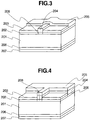
- Cellule solaire comprenant un substrat de silicium cristallin (201, 401) d'un type de conductivité ayant une surface de réception de lumière, une couche émettrice (202, 402) formée sur le côté surface de réception de lumière du substrat et ayant un dopant d'un type de conductivité opposé ajouté à celle-ci, un film de passivation (203, 403a) formé sur la surface du substrat, une électrode d'extraction pour extraire une charge photo-générée du substrat de silicium, et une électrode collectrice en contact avec au moins une partie de l'électrode d'extraction pour collecter la charge attirée dans l'électrode d'extraction, dans laquelle
l'électrode d'extraction inclut une première électrode (204, 404a), l'électrode collectrice inclut une seconde électrode (205, 405a), et la première électrode (204, 404a) est partiellement en contact ou entièrement recouverte avec la seconde électrode (205, 405),
caractérisée en ce que
la première électrode est sous une forme pouvant être obtenue par frittage d'une pâte conductrice contenant de la poudre d'argent, de la fritte de verre et un dopant pour conférer une conductivité au silicium, la première électrode (204, 404a) pénétrant à travers le film de passivation (203, 403a), moyennant quoi en dessous de l'interface entre la couche émettrice (202, 402) et la première électrode (204, 404a), se trouve une région auto-dopée (208, 407a) en résultat de la diffusion de dopant supplémentaire à partir de la première électrode pendant le frittage, et
l'électrode collectrice inclut une seconde électrode (205, 405a) pouvant être obtenue par cuisson d'une pâte conductrice contenant une proportion plus élevée de poudre d'argent que ladite pâte conductrice formant la première électrode, et ayant une conductivité plus élevée que la première électrode (204, 404a). - Cellule solaire selon la revendication 1, dans laquelle la région auto-dopée (208, 407a) a une résisitivité plus faible que la couche émettrice (202, 402) disposée de manière adjacente à celle-ci.
- Cellule solaire selon la revendication 1 ou la revendication 2, dans laquelle la première électrode (204, 404a) est formée d'une pâte conductrice à base de Ag et contenant B, Al, Ga, P, As, In ou Sb, seuls ou sous forme d'un composé de ceux-ci ou d'une combinaison de ceux-ci, en tant que dopant.
- Cellule solaire selon l'une quelconque des revendications 1 à 3, dans laquelle l'électrode d'extraction a une structure stratifiée constituée des première et seconde électrodes (204, 205 ; 404a, 405), et l'électrode collectrice a une structure monocouche constituée de la seconde électrode (205, 405).
- Cellule solaire selon l'une quelconque des revendications 1 à 3, dans laquelle l'électrode d'extraction et l'électrode collectrice ont chacune une structure stratifiée constituée des première et seconde électrodes (204, 405).
- Cellule solaire selon l'une quelconque des revendications 1 à 3, dans laquelle l'électrode d'extraction est constituée de la première électrode (204) et l'électrode collectrice est constituée de la seconde électrode (205) .
- Cellule solaire selon l'une quelconque des revendications 1 à 6, dans laquelle le film de passivation comprend de l'oxyde de silicium, du nitrure de silicium, du carbure de silicium, de l'oxyde d'aluminium, du silicium amorphe, du silicium microcristallin ou de l'oxyde de titane ou une combinaison de ceux-ci.
- Cellule solaire selon l'une quelconque des revendications 1 à 7, dans laquelle le substrat de silicium cristallin a une surface non réceptrice de lumière avec un film de passivation de côté arrière (403b) formé sur la surface non réceptrice de lumière du substrat, une électrode d'extraction de côté arrière pour extraire une charge photo-générée du substrat de silicium, et une électrode collectrice de côté arrière disposée au moins partiellement en contact avec l'électrode d'extraction de côté arrière pour collecter la charge collectée dans l'électrode d'extraction de côté arrière, et dans laquelle
l'électrode d'extraction de côté arrière inclut une première électrode de côté arrière (404b) pouvant être obtenue par frittage d'une pâte conductrice contenant un dopant pour conférer une conductivité au silicium, la première électrode de côté arrière (404b) pénétrant à travers le film de passivation de côté arrière (403b), moyennant quoi à l'interface entre le substrat de silicium et la première électrode de côté arrière, se trouve une région auto-dopée (407b) en résultat d'une diffusion de dopant dans la première électrode de côté arrière pendant le frittage,
l'électrode collectrice côté de arrière inclut une seconde électrode de côté arrière (405b) ayant une conductivité plus élevée que la première électrode de côté arrière (404b), et
la première électrode de côté arrière (404b) est partiellement en contact ou entièrement recouverte avec la seconde électrode de côté arrière (405b). - Cellule solaire selon la revendication 8, dans laquelle la première électrode de côté arrière (404b) peut être obtenue par frittage d'une dite pâte conductrice contenant de la poudre d'argent, de la fritte de verre et ledit dopant et la seconde électrode de côté arrière (405b) peut être obtenue par frittage d'une pâte conductrice contenant une proportion plus élevée de poudre d'argent que ladite pâte conductrice formant la première électrode de côté arrière.
- Cellule solaire selon la revendication 8, dans laquelle la région auto-dopée (407b) au niveau de la surface non réceptrice de lumière a une résisitivité plus faible qu'une région non auto-dopée disposée de manière adjacente à celle-ci.
- Module de cellules solaires comprenant des cellules solaires connectées électriquement selon l'une quelconque des revendications 1 à 10.
- Procédé de fabrication d'une cellule solaire selon l'une quelconque des revendications 1 à 10, comprenant(a) sur ledit côté surface de réception de lumière du substrat de silicium cristallin, la formation d'une couche émettrice (202, 402) par ajout de dopant, et la formation du film de passivation (203, 403a) sur ladite surface du substrat, et caractérisé par(b) la formation de la première électrode (204, 404a) par frittage d'une dite pâte conductrice contenant de la poudre d'argent, de la fritte de verre et ledit dopant pour conférer une conductivité au silicium, moyennant quoi pendant ledit frittage la pâte conductrice pénètre dans le film de passivation (203, 403a) pour établir un contact électrique avec le substrat de silicium, et le dopant dans la pâte conductrice se diffuse pour former la région auto-dopée (208, 407a) en dessous de l'interface entre la première électrode (204, 404a) et la couche émettrice, etla formation de la seconde électrode (405a) par cuisson de ladite pâte conductrice contenant une proportion plus élevée de poudre d'argent que ladite pâte conductrice formant la première électrode (404b).
- Procédé selon la revendication 12, dans lequel pour fournir les première et seconde électrodes, la première électrode est imprimée et séchée, la seconde électrode est imprimée, et un traitement thermique unique est réalisé pour faire cuire à la fois les première et seconde électrodes en même temps.
- Procédé selon la revendication 12 ou 13, dans lequel la première électrode (204, 404a) est préparée par sérigraphie de la pâte d'électrode conductrice pour former un motif d'électrodes d'extraction uniquement ou un motif à la fois d'électrodes d'extraction et collectrices, et la seconde électrode (204, 404a) est préparée par sérigraphie de pâte d'électrode conductrice pour former un motif à la fois d'électrodes d'extraction et collectrices ou un motif d'électrodes collectrices uniquement.
- Procédé selon l'une quelconque des revendications 12 à 14 fabriquant une cellule solaire selon la revendication 8, et comprenant :(c) sur ladite surface non réceptrice de lumière du substrat de silicium cristallin, la formation dudit film de passivation de côté arrière (403b), et(d) la formation de la première électrode de côté arrière (404b) par frittage de ladite pâte conductrice contenant du dopant pour procurer une conductivité au silicium, moyennant quoi pendant ledit frittage, la pâte conductrice pénètre dans le film de passivation de côté arrière (403b) et le dopant dans la pâte conductrice se diffuse pour former la région auto-dopée (407b) à l'interface entre la première électrode de côté arrière (404b) et le substrat de silicium, etla formation de la seconde électrode de côté arrière (405b) ayant une conductivité plus élevée que la première électrode de côté arrière (404b).
- Procédé selon la revendication 15, dans lequel la première électrode de côté arrière (404b) est formée par frittage d'une dite pâte conductrice contenant de la poudre d'argent, de la fritte de verre et ledit dopant, et la seconde électrode de côté arrière (405b) est formée par cuisson d'une pâte conductrice contenant une proportion plus élevée de poudre d'argent que ladite pâte conductrice formant la première électrode de côté arrière.
Applications Claiming Priority (2)
| Application Number | Priority Date | Filing Date | Title |
|---|---|---|---|
| JP2010271619 | 2010-12-06 | ||
| PCT/JP2011/077784 WO2012077567A1 (fr) | 2010-12-06 | 2011-12-01 | Cellule solaire et module cellule solaire |
Publications (3)
| Publication Number | Publication Date |
|---|---|
| EP2650923A1 EP2650923A1 (fr) | 2013-10-16 |
| EP2650923A4 EP2650923A4 (fr) | 2017-11-22 |
| EP2650923B1 true EP2650923B1 (fr) | 2021-06-02 |
Family
ID=46207057
Family Applications (1)
| Application Number | Title | Priority Date | Filing Date |
|---|---|---|---|
| EP11846590.5A Active EP2650923B1 (fr) | 2010-12-06 | 2011-12-01 | Cellule solaire, module cellule solaire et methode de fabrication de cellule solaire |
Country Status (11)
| Country | Link |
|---|---|
| US (2) | US20130247957A1 (fr) |
| EP (1) | EP2650923B1 (fr) |
| JP (1) | JP5541370B2 (fr) |
| KR (1) | KR101917879B1 (fr) |
| CN (1) | CN103329280B (fr) |
| CA (1) | CA2820002A1 (fr) |
| MY (1) | MY170106A (fr) |
| RU (1) | RU2571444C2 (fr) |
| SG (1) | SG191044A1 (fr) |
| TW (1) | TWI587534B (fr) |
| WO (1) | WO2012077567A1 (fr) |
Families Citing this family (17)
| Publication number | Priority date | Publication date | Assignee | Title |
|---|---|---|---|---|
| US9293624B2 (en) * | 2012-12-10 | 2016-03-22 | Sunpower Corporation | Methods for electroless plating of a solar cell metallization layer |
| US9263601B2 (en) * | 2012-12-21 | 2016-02-16 | Sunpower Corporation | Enhanced adhesion of seed layer for solar cell conductive contact |
| KR102032280B1 (ko) * | 2013-04-25 | 2019-10-15 | 엘지전자 주식회사 | 태양 전지의 전극용 페이스트 조성물 |
| JP5739076B2 (ja) * | 2013-05-13 | 2015-06-24 | 株式会社カネカ | 太陽電池モジュール及びその製造方法 |
| MY179134A (en) | 2013-05-21 | 2020-10-28 | Kaneka Corp | Solar cell, solar cell module, method for manufacturing solar cell, and method for manufacturing solar cell module |
| JP2015050349A (ja) * | 2013-09-02 | 2015-03-16 | 株式会社ノリタケカンパニーリミテド | 太陽電池素子およびその製造方法並びにファイヤースルー用アルミニウムペースト |
| TW201511300A (zh) * | 2013-09-11 | 2015-03-16 | Inst Nuclear Energy Res Atomic Energy Council | 具有摻雜矽或硼原子之鋁金屬電極之製備方法 |
| KR101867855B1 (ko) | 2014-03-17 | 2018-06-15 | 엘지전자 주식회사 | 태양 전지 |
| JP6388707B2 (ja) * | 2014-04-03 | 2018-09-12 | トリナ ソーラー エナジー デベロップメント ピーティーイー リミテッド | ハイブリッド全バックコンタクト太陽電池及びその製造方法 |
| CN104241454B (zh) * | 2014-09-25 | 2017-04-05 | 上海联孚新能源科技集团有限公司 | 一种提高太阳能电池转化效率的方法 |
| JP6502651B2 (ja) | 2014-11-13 | 2019-04-17 | 信越化学工業株式会社 | 太陽電池の製造方法及び太陽電池モジュールの製造方法 |
| US10061449B2 (en) | 2014-12-04 | 2018-08-28 | Apple Inc. | Coarse scan and targeted active mode scan for touch and stylus |
| WO2018109849A1 (fr) * | 2016-12-13 | 2018-06-21 | 信越化学工業株式会社 | Cellule solaire de type à électrode de surface arrière hautement efficace, module de cellules solaires et système de génération d'énergie solaire |
| CN110047952A (zh) * | 2019-04-04 | 2019-07-23 | 国家电投集团西安太阳能电力有限公司 | 一种太阳能电池Al栅线结构及其制备方法 |
| EP3836239A4 (fr) * | 2019-10-18 | 2022-06-29 | Enecoat Technologies Co.,Ltd. | Élément |
| CN111739985B (zh) * | 2020-08-21 | 2021-01-12 | 浙江晶科能源有限公司 | 太阳能电池及其选择性发射极的制备方法 |
| CN113644145B (zh) * | 2021-10-18 | 2022-02-18 | 浙江晶科能源有限公司 | 太阳能电池及光伏组件 |
Family Cites Families (32)
| Publication number | Priority date | Publication date | Assignee | Title |
|---|---|---|---|---|
| JPH0536998A (ja) * | 1991-07-30 | 1993-02-12 | Sharp Corp | 電極の形成方法 |
| JP2928433B2 (ja) * | 1993-02-23 | 1999-08-03 | シャープ株式会社 | 光電変換素子の製造方法 |
| EP0853822A4 (fr) | 1995-10-05 | 1999-08-18 | Ebara Solar Inc | Pile solaire a emetteur localement profondement diffuse auto-aligne |
| JP2000138386A (ja) | 1998-11-04 | 2000-05-16 | Shin Etsu Chem Co Ltd | 太陽電池の製造方法およびこの方法で製造された太陽電池 |
| US6632730B1 (en) * | 1999-11-23 | 2003-10-14 | Ebara Solar, Inc. | Method for self-doping contacts to a semiconductor |
| KR100812891B1 (ko) | 2000-04-28 | 2008-03-11 | 메르크 파텐트 게엠베하 | 무기물 표면용 에칭 페이스트 |
| JP2002217434A (ja) * | 2001-01-19 | 2002-08-02 | Sharp Corp | 太陽電池、太陽電池用インターコネクターおよびストリング |
| JP2004273826A (ja) | 2003-03-10 | 2004-09-30 | Sharp Corp | 光電変換装置及びその製造方法 |
| JP4121928B2 (ja) | 2003-10-08 | 2008-07-23 | シャープ株式会社 | 太陽電池の製造方法 |
| WO2005109524A1 (fr) * | 2004-05-07 | 2005-11-17 | Mitsubishi Denki Kabushiki Kaisha | Pile solaire et procédé de fabrication de celle-ci |
| JP4557622B2 (ja) * | 2004-07-29 | 2010-10-06 | 京セラ株式会社 | 太陽電池素子の接続構造及びこれを含む太陽電池モジュール |
| JP4780953B2 (ja) | 2004-11-29 | 2011-09-28 | 京セラ株式会社 | 太陽電池素子及び、これを用いた太陽電池モジュール |
| US7435361B2 (en) * | 2005-04-14 | 2008-10-14 | E.I. Du Pont De Nemours And Company | Conductive compositions and processes for use in the manufacture of semiconductor devices |
| JP2008204967A (ja) * | 2005-05-31 | 2008-09-04 | Naoetsu Electronics Co Ltd | 太陽電池素子及びその製造方法 |
| JP2007096040A (ja) | 2005-09-29 | 2007-04-12 | Sharp Corp | 太陽電池の製造方法および太陽電池 |
| US7765949B2 (en) * | 2005-11-17 | 2010-08-03 | Palo Alto Research Center Incorporated | Extrusion/dispensing systems and methods |
| JP2007214372A (ja) * | 2006-02-09 | 2007-08-23 | Sharp Corp | 太陽電池およびその製造方法 |
| JP4963866B2 (ja) | 2006-04-28 | 2012-06-27 | シャープ株式会社 | 光電変換素子の製造方法 |
| TWI487124B (zh) * | 2006-08-25 | 2015-06-01 | Sanyo Electric Co | 太陽電池模組及太陽電池模組的製造方法 |
| TWI419349B (zh) * | 2007-07-26 | 2013-12-11 | Univ Konstanz | 具有回蝕刻射極之矽太陽能電池的製造方法及對應的太陽能電池 |
| US8309844B2 (en) * | 2007-08-29 | 2012-11-13 | Ferro Corporation | Thick film pastes for fire through applications in solar cells |
| JP4610630B2 (ja) * | 2008-03-31 | 2011-01-12 | 三菱電機株式会社 | 太陽電池用拡散層の製造方法および太陽電池セルの製造方法 |
| US20090250108A1 (en) * | 2008-04-02 | 2009-10-08 | Applied Materials, Inc. | Silicon carbide for crystalline silicon solar cell surface passivation |
| KR100974221B1 (ko) | 2008-04-17 | 2010-08-06 | 엘지전자 주식회사 | 레이저 어닐링을 이용한 태양전지의 선택적 에미터형성방법 및 이를 이용한 태양전지의 제조방법 |
| JP5172480B2 (ja) * | 2008-06-04 | 2013-03-27 | シャープ株式会社 | 光電変換装置およびその製造方法 |
| TWI423462B (zh) * | 2008-10-22 | 2014-01-11 | Ind Tech Res Inst | 矽晶太陽電池之背面電極製造方法 |
| KR20120099330A (ko) * | 2008-11-14 | 2012-09-10 | 어플라이드 나노테크 홀딩스, 인크. | 태양 전지 제조를 위한 잉크 및 페이스트 |
| KR100993511B1 (ko) * | 2008-11-19 | 2010-11-12 | 엘지전자 주식회사 | 태양 전지 및 그 제조 방법 |
| KR101002282B1 (ko) * | 2008-12-15 | 2010-12-20 | 엘지전자 주식회사 | 태양 전지 및 그 제조 방법 |
| US8722453B2 (en) * | 2009-04-14 | 2014-05-13 | Mitsubishi Electric Corporation | Photovoltaic device and method for manufacturing the same |
| KR101009422B1 (ko) * | 2009-04-14 | 2011-01-19 | (유)에스엔티 | 태양전지의 제조 방법 |
| US8586129B2 (en) * | 2010-09-01 | 2013-11-19 | Solarworld Innovations Gmbh | Solar cell with structured gridline endpoints and vertices |
-
2011
- 2011-12-01 US US13/991,978 patent/US20130247957A1/en not_active Abandoned
- 2011-12-01 MY MYPI2013002043A patent/MY170106A/en unknown
- 2011-12-01 CA CA2820002A patent/CA2820002A1/fr not_active Abandoned
- 2011-12-01 SG SG2013043831A patent/SG191044A1/en unknown
- 2011-12-01 WO PCT/JP2011/077784 patent/WO2012077567A1/fr active Application Filing
- 2011-12-01 EP EP11846590.5A patent/EP2650923B1/fr active Active
- 2011-12-01 RU RU2013131015/28A patent/RU2571444C2/ru active
- 2011-12-01 KR KR1020137017430A patent/KR101917879B1/ko active IP Right Grant
- 2011-12-01 CN CN201180065728.7A patent/CN103329280B/zh active Active
- 2011-12-01 JP JP2012547809A patent/JP5541370B2/ja active Active
- 2011-12-06 TW TW100144862A patent/TWI587534B/zh active
-
2015
- 2015-10-23 US US14/921,473 patent/US9887312B2/en active Active
Non-Patent Citations (1)
| Title |
|---|
| None * |
Also Published As
| Publication number | Publication date |
|---|---|
| CA2820002A1 (fr) | 2012-06-14 |
| MY170106A (en) | 2019-07-05 |
| WO2012077567A1 (fr) | 2012-06-14 |
| US9887312B2 (en) | 2018-02-06 |
| TWI587534B (zh) | 2017-06-11 |
| CN103329280A (zh) | 2013-09-25 |
| US20130247957A1 (en) | 2013-09-26 |
| EP2650923A4 (fr) | 2017-11-22 |
| RU2571444C2 (ru) | 2015-12-20 |
| KR101917879B1 (ko) | 2018-11-13 |
| JP5541370B2 (ja) | 2014-07-09 |
| EP2650923A1 (fr) | 2013-10-16 |
| KR20130138285A (ko) | 2013-12-18 |
| JPWO2012077567A1 (ja) | 2014-05-19 |
| CN103329280B (zh) | 2017-02-08 |
| TW201240115A (en) | 2012-10-01 |
| RU2013131015A (ru) | 2015-01-20 |
| SG191044A1 (en) | 2013-08-30 |
| US20160079466A1 (en) | 2016-03-17 |
Similar Documents
| Publication | Publication Date | Title |
|---|---|---|
| EP2650923B1 (fr) | Cellule solaire, module cellule solaire et methode de fabrication de cellule solaire | |
| US11545588B2 (en) | Solar cell, method for manufacturing solar cell, and solar cell module | |
| US9224888B2 (en) | Solar cell and solar-cell module | |
| JP5091161B2 (ja) | 太陽電池素子及び太陽電池素子の製造方法 | |
| EP2905812B1 (fr) | Procédé de fabrication de cellule photovoltaïque | |
| KR101149891B1 (ko) | 태양전지 및 이의 제조방법 | |
| JP2014146553A (ja) | 太陽電池の電極用導電性ペーストおよびその製造方法 | |
| Balaji et al. | Laser fired local back contact c-Si solar cells using phosphoric acid for back surface field | |
| JP2011018748A (ja) | 太陽電池セルの製造方法 |
Legal Events
| Date | Code | Title | Description |
|---|---|---|---|
| PUAI | Public reference made under article 153(3) epc to a published international application that has entered the european phase |
Free format text: ORIGINAL CODE: 0009012 |
|
| 17P | Request for examination filed |
Effective date: 20130620 |
|
| AK | Designated contracting states |
Kind code of ref document: A1 Designated state(s): AL AT BE BG CH CY CZ DE DK EE ES FI FR GB GR HR HU IE IS IT LI LT LU LV MC MK MT NL NO PL PT RO RS SE SI SK SM TR |
|
| DAX | Request for extension of the european patent (deleted) | ||
| REG | Reference to a national code |
Ref country code: DE Ref legal event code: R079 Ref document number: 602011071099 Country of ref document: DE Free format text: PREVIOUS MAIN CLASS: H01L0031040000 Ipc: H01L0031022400 |
|
| RA4 | Supplementary search report drawn up and despatched (corrected) |
Effective date: 20171023 |
|
| RIC1 | Information provided on ipc code assigned before grant |
Ipc: H01L 31/18 20060101ALI20171017BHEP Ipc: H01L 31/0224 20060101AFI20171017BHEP Ipc: H01L 31/0216 20140101ALI20171017BHEP Ipc: H01L 31/068 20120101ALI20171017BHEP |
|
| GRAP | Despatch of communication of intention to grant a patent |
Free format text: ORIGINAL CODE: EPIDOSNIGR1 |
|
| STAA | Information on the status of an ep patent application or granted ep patent |
Free format text: STATUS: GRANT OF PATENT IS INTENDED |
|
| INTG | Intention to grant announced |
Effective date: 20201217 |
|
| GRAS | Grant fee paid |
Free format text: ORIGINAL CODE: EPIDOSNIGR3 |
|
| GRAA | (expected) grant |
Free format text: ORIGINAL CODE: 0009210 |
|
| STAA | Information on the status of an ep patent application or granted ep patent |
Free format text: STATUS: THE PATENT HAS BEEN GRANTED |
|
| RBV | Designated contracting states (corrected) |
Designated state(s): DE FR GB NL |
|
| AK | Designated contracting states |
Kind code of ref document: B1 Designated state(s): DE FR GB NL |
|
| REG | Reference to a national code |
Ref country code: GB Ref legal event code: FG4D |
|
| REG | Reference to a national code |
Ref country code: DE Ref legal event code: R096 Ref document number: 602011071099 Country of ref document: DE |
|
| REG | Reference to a national code |
Ref country code: NL Ref legal event code: FP |
|
| REG | Reference to a national code |
Ref country code: DE Ref legal event code: R097 Ref document number: 602011071099 Country of ref document: DE |
|
| PLBE | No opposition filed within time limit |
Free format text: ORIGINAL CODE: 0009261 |
|
| STAA | Information on the status of an ep patent application or granted ep patent |
Free format text: STATUS: NO OPPOSITION FILED WITHIN TIME LIMIT |
|
| 26N | No opposition filed |
Effective date: 20220303 |
|
| P01 | Opt-out of the competence of the unified patent court (upc) registered |
Effective date: 20230512 |
|
| PGFP | Annual fee paid to national office [announced via postgrant information from national office to epo] |
Ref country code: NL Payment date: 20231116 Year of fee payment: 13 |
|
| PGFP | Annual fee paid to national office [announced via postgrant information from national office to epo] |
Ref country code: GB Payment date: 20231102 Year of fee payment: 13 |
|
| PGFP | Annual fee paid to national office [announced via postgrant information from national office to epo] |
Ref country code: FR Payment date: 20231108 Year of fee payment: 13 Ref country code: DE Payment date: 20231031 Year of fee payment: 13 |