EP2649659B1 - Active matrix display comprising a dilute source enabled vertical organic light emitting transistor - Google Patents
Active matrix display comprising a dilute source enabled vertical organic light emitting transistor Download PDFInfo
- Publication number
- EP2649659B1 EP2649659B1 EP11846649.9A EP11846649A EP2649659B1 EP 2649659 B1 EP2649659 B1 EP 2649659B1 EP 11846649 A EP11846649 A EP 11846649A EP 2649659 B1 EP2649659 B1 EP 2649659B1
- Authority
- EP
- European Patent Office
- Prior art keywords
- layer
- source
- volet
- vfet
- dilute
- Prior art date
- Legal status (The legal status is an assumption and is not a legal conclusion. Google has not performed a legal analysis and makes no representation as to the accuracy of the status listed.)
- Active
Links
- 239000011159 matrix material Substances 0.000 title description 7
- OKTJSMMVPCPJKN-UHFFFAOYSA-N Carbon Chemical compound [C] OKTJSMMVPCPJKN-UHFFFAOYSA-N 0.000 claims description 62
- 239000004065 semiconductor Substances 0.000 claims description 52
- 239000002041 carbon nanotube Substances 0.000 claims description 47
- 229910021393 carbon nanotube Inorganic materials 0.000 claims description 46
- 239000000463 material Substances 0.000 claims description 42
- 239000000758 substrate Substances 0.000 claims description 35
- 239000004020 conductor Substances 0.000 claims description 18
- 229910021389 graphene Inorganic materials 0.000 claims description 11
- 239000010409 thin film Substances 0.000 claims description 11
- 238000002347 injection Methods 0.000 claims description 6
- 239000007924 injection Substances 0.000 claims description 6
- 230000000694 effects Effects 0.000 claims description 5
- 230000004913 activation Effects 0.000 claims description 2
- 230000000295 complement effect Effects 0.000 claims 1
- 239000010410 layer Substances 0.000 description 380
- 229910052751 metal Inorganic materials 0.000 description 30
- 239000002184 metal Substances 0.000 description 30
- 238000000034 method Methods 0.000 description 30
- SLIUAWYAILUBJU-UHFFFAOYSA-N pentacene Chemical compound C1=CC=CC2=CC3=CC4=CC5=CC=CC=C5C=C4C=C3C=C21 SLIUAWYAILUBJU-UHFFFAOYSA-N 0.000 description 19
- 229920000642 polymer Polymers 0.000 description 18
- 239000002071 nanotube Substances 0.000 description 16
- -1 polyethylene terephthalate Polymers 0.000 description 16
- 238000000151 deposition Methods 0.000 description 15
- UMIVXZPTRXBADB-UHFFFAOYSA-N benzocyclobutene Chemical compound C1=CC=C2CCC2=C1 UMIVXZPTRXBADB-UHFFFAOYSA-N 0.000 description 14
- 239000000243 solution Substances 0.000 description 14
- 150000003384 small molecules Chemical class 0.000 description 13
- 239000003990 capacitor Substances 0.000 description 11
- 238000004528 spin coating Methods 0.000 description 11
- 238000003860 storage Methods 0.000 description 11
- 230000008021 deposition Effects 0.000 description 10
- 230000001965 increasing effect Effects 0.000 description 10
- 238000010586 diagram Methods 0.000 description 9
- 239000002105 nanoparticle Substances 0.000 description 9
- 238000002441 X-ray diffraction Methods 0.000 description 8
- 238000013461 design Methods 0.000 description 8
- 229920000144 PEDOT:PSS Polymers 0.000 description 7
- XLOMVQKBTHCTTD-UHFFFAOYSA-N Zinc monoxide Chemical compound [Zn]=O XLOMVQKBTHCTTD-UHFFFAOYSA-N 0.000 description 7
- 238000000089 atomic force micrograph Methods 0.000 description 7
- 229910003437 indium oxide Inorganic materials 0.000 description 7
- PJXISJQVUVHSOJ-UHFFFAOYSA-N indium(iii) oxide Chemical compound [O-2].[O-2].[O-2].[In+3].[In+3] PJXISJQVUVHSOJ-UHFFFAOYSA-N 0.000 description 7
- 229910010272 inorganic material Inorganic materials 0.000 description 7
- 239000011147 inorganic material Substances 0.000 description 7
- 239000002904 solvent Substances 0.000 description 7
- 229910052782 aluminium Inorganic materials 0.000 description 6
- XAGFODPZIPBFFR-UHFFFAOYSA-N aluminium Chemical compound [Al] XAGFODPZIPBFFR-UHFFFAOYSA-N 0.000 description 6
- 239000011521 glass Substances 0.000 description 6
- 229920002120 photoresistant polymer Polymers 0.000 description 6
- 229920001609 Poly(3,4-ethylenedioxythiophene) Polymers 0.000 description 5
- 239000002019 doping agent Substances 0.000 description 5
- 238000004519 manufacturing process Methods 0.000 description 5
- 229910000476 molybdenum oxide Inorganic materials 0.000 description 5
- 239000002070 nanowire Substances 0.000 description 5
- TWNQGVIAIRXVLR-UHFFFAOYSA-N oxo(oxoalumanyloxy)alumane Chemical compound O=[Al]O[Al]=O TWNQGVIAIRXVLR-UHFFFAOYSA-N 0.000 description 5
- PQQKPALAQIIWST-UHFFFAOYSA-N oxomolybdenum Chemical compound [Mo]=O PQQKPALAQIIWST-UHFFFAOYSA-N 0.000 description 5
- 238000000623 plasma-assisted chemical vapour deposition Methods 0.000 description 5
- 229920001467 poly(styrenesulfonates) Polymers 0.000 description 5
- 229910021420 polycrystalline silicon Inorganic materials 0.000 description 5
- 230000008569 process Effects 0.000 description 5
- 230000002829 reductive effect Effects 0.000 description 5
- 239000002356 single layer Substances 0.000 description 5
- 230000003746 surface roughness Effects 0.000 description 5
- XEEYBQQBJWHFJM-UHFFFAOYSA-N Iron Chemical compound [Fe] XEEYBQQBJWHFJM-UHFFFAOYSA-N 0.000 description 4
- UQSXHKLRYXJYBZ-UHFFFAOYSA-N Iron oxide Chemical compound [Fe]=O UQSXHKLRYXJYBZ-UHFFFAOYSA-N 0.000 description 4
- XUIMIQQOPSSXEZ-UHFFFAOYSA-N Silicon Chemical compound [Si] XUIMIQQOPSSXEZ-UHFFFAOYSA-N 0.000 description 4
- 238000000231 atomic layer deposition Methods 0.000 description 4
- 230000004888 barrier function Effects 0.000 description 4
- 230000008901 benefit Effects 0.000 description 4
- 239000011248 coating agent Substances 0.000 description 4
- 238000000576 coating method Methods 0.000 description 4
- 230000003247 decreasing effect Effects 0.000 description 4
- 239000010408 film Substances 0.000 description 4
- 238000007647 flexography Methods 0.000 description 4
- 230000006870 function Effects 0.000 description 4
- 238000007646 gravure printing Methods 0.000 description 4
- 238000007641 inkjet printing Methods 0.000 description 4
- PQXKHYXIUOZZFA-UHFFFAOYSA-M lithium fluoride Chemical compound [Li+].[F-] PQXKHYXIUOZZFA-UHFFFAOYSA-M 0.000 description 4
- 230000003071 parasitic effect Effects 0.000 description 4
- 238000000059 patterning Methods 0.000 description 4
- 230000004044 response Effects 0.000 description 4
- 229910052710 silicon Inorganic materials 0.000 description 4
- 239000010703 silicon Substances 0.000 description 4
- 238000004544 sputter deposition Methods 0.000 description 4
- 238000002207 thermal evaporation Methods 0.000 description 4
- 238000002834 transmittance Methods 0.000 description 4
- IXHWGNYCZPISET-UHFFFAOYSA-N 2-[4-(dicyanomethylidene)-2,3,5,6-tetrafluorocyclohexa-2,5-dien-1-ylidene]propanedinitrile Chemical compound FC1=C(F)C(=C(C#N)C#N)C(F)=C(F)C1=C(C#N)C#N IXHWGNYCZPISET-UHFFFAOYSA-N 0.000 description 3
- LGDCSNDMFFFSHY-UHFFFAOYSA-N 4-butyl-n,n-diphenylaniline Polymers C1=CC(CCCC)=CC=C1N(C=1C=CC=CC=1)C1=CC=CC=C1 LGDCSNDMFFFSHY-UHFFFAOYSA-N 0.000 description 3
- 229920001621 AMOLED Polymers 0.000 description 3
- 239000004642 Polyimide Substances 0.000 description 3
- YXFVVABEGXRONW-UHFFFAOYSA-N Toluene Chemical compound CC1=CC=CC=C1 YXFVVABEGXRONW-UHFFFAOYSA-N 0.000 description 3
- 229910052799 carbon Inorganic materials 0.000 description 3
- 239000002238 carbon nanotube film Substances 0.000 description 3
- 238000005266 casting Methods 0.000 description 3
- 238000006243 chemical reaction Methods 0.000 description 3
- 238000003618 dip coating Methods 0.000 description 3
- 238000005516 engineering process Methods 0.000 description 3
- 230000006872 improvement Effects 0.000 description 3
- 239000011810 insulating material Substances 0.000 description 3
- 229910044991 metal oxide Inorganic materials 0.000 description 3
- 150000004706 metal oxides Chemical class 0.000 description 3
- 238000000206 photolithography Methods 0.000 description 3
- 229920001721 polyimide Polymers 0.000 description 3
- 238000007639 printing Methods 0.000 description 3
- 230000009467 reduction Effects 0.000 description 3
- 238000007650 screen-printing Methods 0.000 description 3
- 239000002094 self assembled monolayer Substances 0.000 description 3
- 239000013545 self-assembled monolayer Substances 0.000 description 3
- VYPSYNLAJGMNEJ-UHFFFAOYSA-N silicon dioxide Inorganic materials O=[Si]=O VYPSYNLAJGMNEJ-UHFFFAOYSA-N 0.000 description 3
- 239000002109 single walled nanotube Substances 0.000 description 3
- 238000005507 spraying Methods 0.000 description 3
- 238000010345 tape casting Methods 0.000 description 3
- ZMKRXXDBXFWSQZ-UHFFFAOYSA-N tris(2,4,6-trimethyl-6-pyridin-3-ylcyclohexa-2,4-dien-1-yl)borane Chemical compound CC1=CC(C)=CC(C)(C=2C=NC=CC=2)C1B(C1C(C=C(C)C=C1C)(C)C=1C=NC=CC=1)C1C(C)=CC(C)=CC1(C)C1=CC=CN=C1 ZMKRXXDBXFWSQZ-UHFFFAOYSA-N 0.000 description 3
- 239000011787 zinc oxide Substances 0.000 description 3
- VEXZGXHMUGYJMC-UHFFFAOYSA-M Chloride anion Chemical compound [Cl-] VEXZGXHMUGYJMC-UHFFFAOYSA-M 0.000 description 2
- 229910002785 ReO3 Inorganic materials 0.000 description 2
- 229910052581 Si3N4 Inorganic materials 0.000 description 2
- ATJFFYVFTNAWJD-UHFFFAOYSA-N Tin Chemical compound [Sn] ATJFFYVFTNAWJD-UHFFFAOYSA-N 0.000 description 2
- VMPVEPPRYRXYNP-UHFFFAOYSA-I antimony(5+);pentachloride Chemical compound Cl[Sb](Cl)(Cl)(Cl)Cl VMPVEPPRYRXYNP-UHFFFAOYSA-I 0.000 description 2
- 238000004630 atomic force microscopy Methods 0.000 description 2
- 230000008859 change Effects 0.000 description 2
- 239000003086 colorant Substances 0.000 description 2
- 238000004891 communication Methods 0.000 description 2
- 239000002322 conducting polymer Substances 0.000 description 2
- 229920001940 conductive polymer Polymers 0.000 description 2
- 238000011161 development Methods 0.000 description 2
- 238000007599 discharging Methods 0.000 description 2
- 238000001035 drying Methods 0.000 description 2
- 238000005530 etching Methods 0.000 description 2
- 230000002349 favourable effect Effects 0.000 description 2
- 230000005669 field effect Effects 0.000 description 2
- NSABRUJKERBGOU-UHFFFAOYSA-N iridium(3+);2-phenylpyridine Chemical compound [Ir+3].[C-]1=CC=CC=C1C1=CC=CC=N1.[C-]1=CC=CC=C1C1=CC=CC=N1.[C-]1=CC=CC=C1C1=CC=CC=N1 NSABRUJKERBGOU-UHFFFAOYSA-N 0.000 description 2
- 229910052742 iron Inorganic materials 0.000 description 2
- FTMKAMVLFVRZQX-UHFFFAOYSA-N octadecylphosphonic acid Chemical compound CCCCCCCCCCCCCCCCCCP(O)(O)=O FTMKAMVLFVRZQX-UHFFFAOYSA-N 0.000 description 2
- 229920003023 plastic Polymers 0.000 description 2
- 239000004033 plastic Substances 0.000 description 2
- 229920000139 polyethylene terephthalate Polymers 0.000 description 2
- 239000005020 polyethylene terephthalate Substances 0.000 description 2
- YSZJKUDBYALHQE-UHFFFAOYSA-N rhenium trioxide Chemical compound O=[Re](=O)=O YSZJKUDBYALHQE-UHFFFAOYSA-N 0.000 description 2
- HQVNEWCFYHHQES-UHFFFAOYSA-N silicon nitride Chemical compound N12[Si]34N5[Si]62N3[Si]51N64 HQVNEWCFYHHQES-UHFFFAOYSA-N 0.000 description 2
- 229910052814 silicon oxide Inorganic materials 0.000 description 2
- 238000012546 transfer Methods 0.000 description 2
- 239000012780 transparent material Substances 0.000 description 2
- ZNOKGRXACCSDPY-UHFFFAOYSA-N tungsten(VI) oxide Inorganic materials O=[W](=O)=O ZNOKGRXACCSDPY-UHFFFAOYSA-N 0.000 description 2
- 125000001637 1-naphthyl group Chemical group [H]C1=C([H])C([H])=C2C(*)=C([H])C([H])=C([H])C2=C1[H] 0.000 description 1
- DDCBCMPRTJJARO-UHFFFAOYSA-N 3,6-bis(dicyanomethylidene)-2,5-difluorocyclohexa-1,4-diene-1,4-dicarbonitrile Chemical compound FC1=C(C#N)C(=C(C#N)C#N)C(F)=C(C#N)C1=C(C#N)C#N DDCBCMPRTJJARO-UHFFFAOYSA-N 0.000 description 1
- ZOKIJILZFXPFTO-UHFFFAOYSA-N 4-methyl-n-[4-[1-[4-(4-methyl-n-(4-methylphenyl)anilino)phenyl]cyclohexyl]phenyl]-n-(4-methylphenyl)aniline Chemical compound C1=CC(C)=CC=C1N(C=1C=CC(=CC=1)C1(CCCCC1)C=1C=CC(=CC=1)N(C=1C=CC(C)=CC=1)C=1C=CC(C)=CC=1)C1=CC=C(C)C=C1 ZOKIJILZFXPFTO-UHFFFAOYSA-N 0.000 description 1
- ZOXJGFHDIHLPTG-UHFFFAOYSA-N Boron Chemical compound [B] ZOXJGFHDIHLPTG-UHFFFAOYSA-N 0.000 description 1
- XDTMQSROBMDMFD-UHFFFAOYSA-N Cyclohexane Chemical compound C1CCCCC1 XDTMQSROBMDMFD-UHFFFAOYSA-N 0.000 description 1
- 229910002601 GaN Inorganic materials 0.000 description 1
- JMASRVWKEDWRBT-UHFFFAOYSA-N Gallium nitride Chemical compound [Ga]#N JMASRVWKEDWRBT-UHFFFAOYSA-N 0.000 description 1
- GPXJNWSHGFTCBW-UHFFFAOYSA-N Indium phosphide Chemical compound [In]#P GPXJNWSHGFTCBW-UHFFFAOYSA-N 0.000 description 1
- PXHVJJICTQNCMI-UHFFFAOYSA-N Nickel Chemical compound [Ni] PXHVJJICTQNCMI-UHFFFAOYSA-N 0.000 description 1
- BQCADISMDOOEFD-UHFFFAOYSA-N Silver Chemical compound [Ag] BQCADISMDOOEFD-UHFFFAOYSA-N 0.000 description 1
- 239000002042 Silver nanowire Substances 0.000 description 1
- 230000002411 adverse Effects 0.000 description 1
- PNEYBMLMFCGWSK-UHFFFAOYSA-N aluminium oxide Inorganic materials [O-2].[O-2].[O-2].[Al+3].[Al+3] PNEYBMLMFCGWSK-UHFFFAOYSA-N 0.000 description 1
- 229910003481 amorphous carbon Inorganic materials 0.000 description 1
- 229920006125 amorphous polymer Polymers 0.000 description 1
- 229910021417 amorphous silicon Inorganic materials 0.000 description 1
- 238000000137 annealing Methods 0.000 description 1
- 238000003491 array Methods 0.000 description 1
- 229910052785 arsenic Inorganic materials 0.000 description 1
- RQNWIZPPADIBDY-UHFFFAOYSA-N arsenic atom Chemical compound [As] RQNWIZPPADIBDY-UHFFFAOYSA-N 0.000 description 1
- 230000009286 beneficial effect Effects 0.000 description 1
- 239000004305 biphenyl Substances 0.000 description 1
- 230000000903 blocking effect Effects 0.000 description 1
- 229910052796 boron Inorganic materials 0.000 description 1
- 238000004364 calculation method Methods 0.000 description 1
- 238000005229 chemical vapour deposition Methods 0.000 description 1
- 239000011370 conductive nanoparticle Substances 0.000 description 1
- 238000007796 conventional method Methods 0.000 description 1
- 229910052593 corundum Inorganic materials 0.000 description 1
- 238000010168 coupling process Methods 0.000 description 1
- 238000005859 coupling reaction Methods 0.000 description 1
- 238000004132 cross linking Methods 0.000 description 1
- 239000013078 crystal Substances 0.000 description 1
- 238000009713 electroplating Methods 0.000 description 1
- 230000002708 enhancing effect Effects 0.000 description 1
- 230000008020 evaporation Effects 0.000 description 1
- 238000001704 evaporation Methods 0.000 description 1
- 238000002474 experimental method Methods 0.000 description 1
- PCHJSUWPFVWCPO-UHFFFAOYSA-N gold Chemical compound [Au] PCHJSUWPFVWCPO-UHFFFAOYSA-N 0.000 description 1
- 229910002804 graphite Inorganic materials 0.000 description 1
- 239000010439 graphite Substances 0.000 description 1
- 229910000449 hafnium oxide Inorganic materials 0.000 description 1
- WIHZLLGSGQNAGK-UHFFFAOYSA-N hafnium(4+);oxygen(2-) Chemical compound [O-2].[O-2].[Hf+4] WIHZLLGSGQNAGK-UHFFFAOYSA-N 0.000 description 1
- 230000005525 hole transport Effects 0.000 description 1
- BHEPBYXIRTUNPN-UHFFFAOYSA-N hydridophosphorus(.) (triplet) Chemical compound [PH] BHEPBYXIRTUNPN-UHFFFAOYSA-N 0.000 description 1
- 238000010348 incorporation Methods 0.000 description 1
- 238000002329 infrared spectrum Methods 0.000 description 1
- 239000011229 interlayer Substances 0.000 description 1
- 230000000670 limiting effect Effects 0.000 description 1
- 238000004020 luminiscence type Methods 0.000 description 1
- 238000005259 measurement Methods 0.000 description 1
- 150000002739 metals Chemical class 0.000 description 1
- 239000000203 mixture Substances 0.000 description 1
- 238000012986 modification Methods 0.000 description 1
- 230000004048 modification Effects 0.000 description 1
- 239000002048 multi walled nanotube Substances 0.000 description 1
- 230000003287 optical effect Effects 0.000 description 1
- 239000011368 organic material Substances 0.000 description 1
- 125000001997 phenyl group Chemical group [H]C1=C([H])C([H])=C(*)C([H])=C1[H] 0.000 description 1
- 238000005240 physical vapour deposition Methods 0.000 description 1
- 239000011112 polyethylene naphthalate Substances 0.000 description 1
- 239000002861 polymer material Substances 0.000 description 1
- 230000001681 protective effect Effects 0.000 description 1
- 239000010453 quartz Substances 0.000 description 1
- 238000011160 research Methods 0.000 description 1
- 230000002441 reversible effect Effects 0.000 description 1
- 238000004904 shortening Methods 0.000 description 1
- 239000007790 solid phase Substances 0.000 description 1
- 229910001220 stainless steel Inorganic materials 0.000 description 1
- 239000010935 stainless steel Substances 0.000 description 1
- 238000000859 sublimation Methods 0.000 description 1
- 230000008022 sublimation Effects 0.000 description 1
- 239000002562 thickening agent Substances 0.000 description 1
- 238000012876 topography Methods 0.000 description 1
- 238000003828 vacuum filtration Methods 0.000 description 1
- 229910001845 yogo sapphire Inorganic materials 0.000 description 1
Images


Classifications
-
- H—ELECTRICITY
- H10—SEMICONDUCTOR DEVICES; ELECTRIC SOLID-STATE DEVICES NOT OTHERWISE PROVIDED FOR
- H10K—ORGANIC ELECTRIC SOLID-STATE DEVICES
- H10K59/00—Integrated devices, or assemblies of multiple devices, comprising at least one organic light-emitting element covered by group H10K50/00
- H10K59/10—OLED displays
- H10K59/12—Active-matrix OLED [AMOLED] displays
- H10K59/125—Active-matrix OLED [AMOLED] displays including organic TFTs [OTFT]
-
- H—ELECTRICITY
- H10—SEMICONDUCTOR DEVICES; ELECTRIC SOLID-STATE DEVICES NOT OTHERWISE PROVIDED FOR
- H10D—INORGANIC ELECTRIC SEMICONDUCTOR DEVICES
- H10D62/00—Semiconductor bodies, or regions thereof, of devices having potential barriers
- H10D62/80—Semiconductor bodies, or regions thereof, of devices having potential barriers characterised by the materials
- H10D62/881—Semiconductor bodies, or regions thereof, of devices having potential barriers characterised by the materials being a two-dimensional material
- H10D62/882—Graphene
-
- H—ELECTRICITY
- H10—SEMICONDUCTOR DEVICES; ELECTRIC SOLID-STATE DEVICES NOT OTHERWISE PROVIDED FOR
- H10D—INORGANIC ELECTRIC SEMICONDUCTOR DEVICES
- H10D30/00—Field-effect transistors [FET]
- H10D30/60—Insulated-gate field-effect transistors [IGFET]
- H10D30/63—Vertical IGFETs
-
- H—ELECTRICITY
- H10—SEMICONDUCTOR DEVICES; ELECTRIC SOLID-STATE DEVICES NOT OTHERWISE PROVIDED FOR
- H10K—ORGANIC ELECTRIC SOLID-STATE DEVICES
- H10K10/00—Organic devices specially adapted for rectifying, amplifying, oscillating or switching; Organic capacitors or resistors having potential barriers
- H10K10/40—Organic transistors
- H10K10/46—Field-effect transistors, e.g. organic thin-film transistors [OTFT]
- H10K10/462—Insulated gate field-effect transistors [IGFETs]
- H10K10/491—Vertical transistors, e.g. vertical carbon nanotube field effect transistors [CNT-FETs]
-
- H—ELECTRICITY
- H10—SEMICONDUCTOR DEVICES; ELECTRIC SOLID-STATE DEVICES NOT OTHERWISE PROVIDED FOR
- H10K—ORGANIC ELECTRIC SOLID-STATE DEVICES
- H10K10/00—Organic devices specially adapted for rectifying, amplifying, oscillating or switching; Organic capacitors or resistors having potential barriers
- H10K10/80—Constructional details
- H10K10/82—Electrodes
-
- H—ELECTRICITY
- H10—SEMICONDUCTOR DEVICES; ELECTRIC SOLID-STATE DEVICES NOT OTHERWISE PROVIDED FOR
- H10K—ORGANIC ELECTRIC SOLID-STATE DEVICES
- H10K50/00—Organic light-emitting devices
- H10K50/30—Organic light-emitting transistors
-
- H—ELECTRICITY
- H10—SEMICONDUCTOR DEVICES; ELECTRIC SOLID-STATE DEVICES NOT OTHERWISE PROVIDED FOR
- H10K—ORGANIC ELECTRIC SOLID-STATE DEVICES
- H10K50/00—Organic light-emitting devices
- H10K50/80—Constructional details
- H10K50/805—Electrodes
-
- H—ELECTRICITY
- H10—SEMICONDUCTOR DEVICES; ELECTRIC SOLID-STATE DEVICES NOT OTHERWISE PROVIDED FOR
- H10K—ORGANIC ELECTRIC SOLID-STATE DEVICES
- H10K59/00—Integrated devices, or assemblies of multiple devices, comprising at least one organic light-emitting element covered by group H10K50/00
- H10K59/10—OLED displays
- H10K59/12—Active-matrix OLED [AMOLED] displays
- H10K59/121—Active-matrix OLED [AMOLED] displays characterised by the geometry or disposition of pixel elements
- H10K59/1213—Active-matrix OLED [AMOLED] displays characterised by the geometry or disposition of pixel elements the pixel elements being TFTs
-
- H—ELECTRICITY
- H10—SEMICONDUCTOR DEVICES; ELECTRIC SOLID-STATE DEVICES NOT OTHERWISE PROVIDED FOR
- H10K—ORGANIC ELECTRIC SOLID-STATE DEVICES
- H10K71/00—Manufacture or treatment specially adapted for the organic devices covered by this subclass
-
- H—ELECTRICITY
- H10—SEMICONDUCTOR DEVICES; ELECTRIC SOLID-STATE DEVICES NOT OTHERWISE PROVIDED FOR
- H10K—ORGANIC ELECTRIC SOLID-STATE DEVICES
- H10K85/00—Organic materials used in the body or electrodes of devices covered by this subclass
- H10K85/20—Carbon compounds, e.g. carbon nanotubes or fullerenes
- H10K85/221—Carbon nanotubes
-
- B—PERFORMING OPERATIONS; TRANSPORTING
- B82—NANOTECHNOLOGY
- B82Y—SPECIFIC USES OR APPLICATIONS OF NANOSTRUCTURES; MEASUREMENT OR ANALYSIS OF NANOSTRUCTURES; MANUFACTURE OR TREATMENT OF NANOSTRUCTURES
- B82Y99/00—Subject matter not provided for in other groups of this subclass
-
- H—ELECTRICITY
- H10—SEMICONDUCTOR DEVICES; ELECTRIC SOLID-STATE DEVICES NOT OTHERWISE PROVIDED FOR
- H10K—ORGANIC ELECTRIC SOLID-STATE DEVICES
- H10K85/00—Organic materials used in the body or electrodes of devices covered by this subclass
- H10K85/20—Carbon compounds, e.g. carbon nanotubes or fullerenes
Definitions
- WO2009036071 (A ) discloses a vertical light emitting organic transistor comprising carbon nanotube network as a source electrode.
- AMDS-VOLETs active matrix dilute source enabled vertical organic light emitting transistors
- a technological conversion is taking place from existing display technologies to active matrix organic light emitting diode (AMOLED) displays.
- a roadblock to this conversion is supplying the high drive currents needed by the organic light emitting diodes (OLEDs) from thin film transistors (TFTs) in the backplane.
- TFTs thin film transistors
- Using polycrystalline silicon (poly-Si) as the channel material is an option to achieve the high drive currents, but poly-Si adds high manufacturing costs and has non-uniformity issues.
- Organic semiconductor materials for the TFT channel material may be less expensive, but organic semiconductor materials cannot compete with the output currents of poly-Si.
- One way to achieve high output current using an organic semiconductor material is to make the channel length of the TFT short.
- shortening the channel length involves placing the source and drain terminals of the TFT very close to each other.
- This can be expensive due to the need for high resolution patterning.
- a dilute source enabled, vertical-field effect transistor (DS-VFET) circumvents this issue.
- the channel length of a DS-VFET is defined by the thickness of the semiconductor thin film channel layer, leading to sub-micron channels lengths without using high resolution patterning. This allows the high drive currents useful for operating OLEDs at a power consumption comparable to poly-Si TFTs.
- a DS-VFET may also be converted to a device that itself emits light, thereby reducing the number of components needed in the pixel backplane.
- a DS-VFET light emitting combination device is termed the dilute source enabled vertical organic light emitting transistor (DS-VOLET).
- the present application describes various embodiments of a display panel, pixel, and active cell including a DS-VOLET.
- a driving transistor and charge storage capacitor reside next to the OLED device occupying pixel area and thus reduces the aperture ratio (the ratio of the OLED light emitting area to the total pixel area).
- the DS-VOLET includes the driving transistor and storage capacitor as part of its structure, allowing the DS-VOLET to be larger and, thus, increase the light emitting area. This also simplifies the manufacturing process as fewer discrete circuit components are needed.
- the DS-VOLET is coupled to a switching transistor (Sw-T), and various embodiments of the Sw-T will be described below as well.
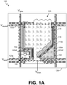
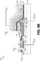
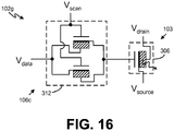
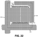
- FIG. 1A is a plan view of an example layout of an embodiment of an active matrix dilute source-enabled vertical organic light emitting transistor (AMDS-VOLET) pixel 100.
- the AMDS-VOLET pixel 100 includes an embodiment of an active cell 102, which lies in the area surrounded by conducting lines 123, as shown in FIG. 1A .
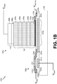
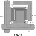
- FIG. 1B provides a cross-sectional view of an embodiment of the active cell 102 illustrated in FIG. 1A , denoted herein as 102a.
- the active cell 102 illustrated in FIGS. 1A and 1B includes an example layout of an embodiment of a DS-VOLET 103.
- a switching transistor (Sw-T) 106 (represented by a transistor circuit element) is coupled to the DS-VOLET 103 and the conducting lines 123, denoted herein as 123a1, 123a2, 123b, 123c, and 123d.
- the layouts of various embodiments of the Sw-T 106 will be discussed in detail below.
- the conducting lines 123 included in the embodiment of an AMDS-VOLET pixel 100 illustrated in FIGS. 1A and 1B includes two data conducting lines 123a, denoted herein as 123a1 and 123a2, that each provide a respective V data voltage signal.
- the conducting lines 123 further include a source conducting line 123b ( i.e., providing a V source voltage signal) and a scan conducting line 123c ( i.e., providing a V scan voltage signal). Additionally, a conducting line 123d couples the Sw-T 106 to the DS-VOLET 103.
- the DS-VOLET 103 is the light emitting component of the AMDS-VOLET pixel 100. Instead of including a separate driving transistor and charge storage capacitor in the AMDS-VOLET pixel 100, the DS-VOLET 103 incorporates the driving transistor and storage capacitor within the stack of the DS-VOLET 103. By including the driving transistor and storage capacitor within the stack of the DS-VOLET 103, a driving transistor and storage capacitor that are separate from the DS-VOLET 103 are unnecessary. Moreover, because the driving transistor and storage capacitor are included within the DS-VOLET 103, the light emitting portion of the AMDS-VOLET pixel 100 is larger than the light emitting portion of a conventional pixel.
- the increase in the light emitting portion increases the aperture ratio of the AMDS-VOLET pixel 100.
- This increase in the light emitting portion enables the AMDS-VOLET pixel 100 to output the same light intensity as conventional pixels, but the AMDS-VOLET pixel 100 uses a lower current density, which may increase the lifetime of the AMDS-VOLET pixel 100.
- the Sw-T 106 is designed to be small in order to reduce the pixel area consumed by the Sw-T 106 and increase the pixel area used by the DS-VOLET 103.
- the storage capacitor in active matrix arrays that use a thin-film transistor (TFT) architecture driving transistor provides additional charge storage ability to the existing gate capacitance of the driving transistor.
- the total capacitance i.e. the sum of the gate and storage capacitor capacitances, should be large enough to retain the majority of the data charge between refreshing events in the operating cycle of the array.
- the architecture of the DS-VOLET 103 is such that it has a large gated area, and therefore more gate capacitance than needed to retain the majority of the data charge between refreshing events, without a separate storage capacitor. This is because the gated area can be as large as the light emitting area of the AMDS-VOLET pixel 100, which can be most ( i.e .
- the DS-VOLET 103 has both a large gated area and aperture ratio because the gate layers and substrate can be transparent, as described below. However, if the gate capacitance becomes too large, there is a concern of insufficient switching speed of the DS-VOLET 103. The larger the gate capacitance, the lower the switching speed. Switching speed measurements are presented below and shown to be sufficiently fast to not limit the switching speed of the AMDS-VOLET pixel 100 in typical display applications.
- the DS-VOLET 103 includes a gate layer 109 (denoted herein as 109a), a source layer 113 (denoted herein as 113a), an active layer 116, and a drain layer 119. These layers will be discussed further below in connection with the description of FIG. 1B .
- the Sw-T 106 is coupled to data conducting line 123a1 that transmits the V data signal, and the Sw-T 106 is also coupled to the gate layer 109a of the DS-VOLET 103 by conducting line 123d.
- the Sw-T 106 is activated at regular intervals by the scan conducting line 123c coupled to a gate 109 of the Sw-T 106 that provides the V scan voltage signal.
- the activation of the Sw-T 106 causes the V data signal to be transmitted to the gate layer 109a of the DS-VOLET 103.
- the Sw-T 106 selectively provides a voltage (e.g., V data ) to the gate layer 109a of the DS-VOLET 103 to control the grayscale of the DS-VOLET 103.
- the V source and V drain signals respectively provide voltage across the source layer 113a and drain layer 119 of the DS-VOLET 103.
- the active cell 102a includes an embodiment of a Sw-T 106, denoted herein as 106a.
- the Sw-T 106a is a TFT.
- the active cell 102a also includes an embodiment of a DS-VOLET 103 (denoted herein as 103a).
- the DS-VOLET 103a and Sw-T 106a each include a gate layer 109, denoted herein as 109a and 109b, respectively.
- the gate layers 109a, 109b may be formed according to the same process or independently of each other instead.
- the gate layers 109a, 109b are in direct contact with the substrate layer 126, which may include a material transparent to visible light.
- the substrate layer 126 may include a glass, a quartz, a plastic substrate, and/or another transparent material.
- the substrate layer 126 may be rigid or flexible in nature.
- Potential plastic materials for the substrate layer 126 include, but are not limited to, polyimide, polyethylene terephthalate (PET), and polyethylene naphthalate (PEN).
- PET polyethylene terephthalate
- PEN polyethylene naphthalate
- the substrate layer 126 may be non-transparent, and the substrate layer 126 may include an insulating material without any restriction on the optical properties of the insulating material.
- the AMDS-VOLET pixel 100 may be used in a top emission display, and the substrate layer 126 included in the AMDS-VOLET pixel 100 is non-transparent.
- the substrate layer 126 may also include a metal such as stainless steel. The metal may be of a certain thickness to allow mechanical flexibility.
- an insulating base layer is deposited prior to all other layers to prevent electrical communication between the AMDS-VOLET pixel 100 and the metal substrate layer 126.
- This insulating base layer may include silicon oxide, silicon nitride or a solution processable insulating polymer such as polyimide.
- the insulating base layer may be deposited by plasma enhanced chemical vapor deposition (PECVD), atomic layer deposition (ALD), spin coating or another deposition method mentioned below.
- Each of the gate layers 109a, 109b includes a gate electrode 201 and a gate dielectric layer 202.
- the gate layer 109a is shown as a single layer in FIG. 1A for simplicity.
- the gate electrodes 201 are patterned to correspond to the DS-VOLET 103a and the Sw-T 106a, respectively, and are denoted herein as DS-VOLET gate electrode 201a and Sw-T gate electrode 201b. At least a portion of the gate electrodes 201 are electrically insulated by the gate dielectric layer 202.
- the gate dielectric layer 202 is patterned to correspond to the DS-VOLET 103a and the Sw-T 106a, respectively, denoted herein as DS-VOLET gate dielectric 202a and Sw-T gate dielectric 202b.
- the gate electrodes 201 include a transparent conducting layer, and the gate dielectric layer 202 includes a transparent dielectric coating. In other embodiments, the gate electrodes 201 are non-transparent.
- the gate electrodes 201 may include a single layer or multiple layers of a conducting material such as, for example, an organic or inorganic conducting material, a transparent or non-transparent metal, a semi-metal and/or a semiconductor (doped or undoped, preferably doped).
- a conducting material such as, for example, an organic or inorganic conducting material, a transparent or non-transparent metal, a semi-metal and/or a semiconductor (doped or undoped, preferably doped).
- the term "conductor” can be used to refer to a semiconducting material or semi-metal that has been doped to increase its carrier density such that it is treated as a conductor.
- the gate electrodes 201 are: single or multi-layer graphene, a dilute network or a non-dilute layer of carbon nanotubes (CNTs), tin-doped indium oxide (ITO), poly(3,4-ethylenedioxythiophene) poly(styrene-sulfonate) (PEDOT:PSS), ZnO and/or indium oxide nanoparticles.
- the gate dielectric layer 202 may also include a bi-layer of an inorganic material such as aluminum oxide and a polymer such as benzocyclobutene (BCB). The inorganic material provides a large capacitance, and the polymer serves as a hydrophobizing layer. These layers may be deposited by PECVD, ALD, spin coating or other known methods.
- the gate dielectric 202a is positioned on the gate electrode 201a to electrically isolate the gate electrode 201a from other layers included in the DS-VOLET 103a.
- the DS-VOLET gate electrode 201a and Sw-T gate electrode 201b may be deposited and patterned at the same time.
- the gate dielectric layer 202 may be deposited and patterned for the DS-VOLET gate dielectric 202a and Sw-T gate dielectric 202b at the same time. These layers can also be deposited separately.
- the source layer 113a includes a dilute source material comprising a percolating dilute network.
- a percolating dilute network can be any dilute and electrically percolating material such as, e.g., any low density of states conductor, nanostructured conductor or semiconductor, nanopatterned conductor or semiconductor, low density of states semiconductor, inorganic or organic; or low density of states semi-metal, inorganic or organic.
- An example of a low density of states semi-metal is graphene. Graphene may be single layered or multi-layered and may be patterned to include perforations or un-patterned.
- a low density of states conductor includes metallic single-wall and multi-wall carbon nanotubes, which have an intrinsic low density of states and can further be deposited in a low density, into what is referred to as a dilute network.
- Other examples of a low density of states semiconductor include semiconducting carbon nanotubes and most all organic semiconductors.
- nanostructured semiconductors include Si nanowires, zinc oxide nanowires, indium phosphide nanowires, gallium nitride nanowires.
- nanostructured conductors include silver nanowires, gold nanowires and nickel nanowires.
- organic semiconductor refers to any organic based small molecule, oligomer or polymer known to have semiconducting properties.
- dilute network refers to a thin-film or network included in the source layer 113a having perforations with substantial regions of the dielectric layer 202a not covered by the thin-film or network.
- the source layer 113a may be sufficiently dilute to expose the underlying surface in the range of, e.g., about 0.1% to about 99.9%, about 30% to about 90%, and about 50% to about 80%.
- percolating refers to: (i) a nanotube or nanowire source layer 113a having a density of nanotubes ( i .
- Dilute can also refer to graphene, which is considered a dilute source material because it has a low density of states and therefore can be used with or without perforations.
- a dilute network of carbon nanotubes is used as the source electrode of the DS-VOLET 103a.
- an active cell 102b including a dilute network of single-wall carbon nanotubes as the source layer 113b which may be referred to as a carbon nanotube-enabled vertical organic light emitting transistor (CN-VOLET) 103b.
- the dilute nanotube network source layer 113b is positioned on the CN-VOLET gate dielectric 202a over the CN-VOLET gate electrode 201a.
- Patent Application Publication US 2010/0237336 having Serial No. 12/677,457 , entitled “Nanotube Enabled, Gate-Voltage Controlled Light Emitting Diodes” and filed September 10, 2008; International Publication WO 2011/109693 A2 , having International Application No. PCT/US2011/027155 , entitled “Semiconductor Devices Including an Electrically Percolating Source Layer and Methods of Fabricating the Same” and filed March 4, 2011; and U.S. Provisional Application entitled “Semiconductor Devices Including a Nanotube Layer and a Memory Layer and Methods of Fabricating the Same” having Ser. No. 61/310,342 and being filed on March 4, 2010.
- the gate electrode 201a and the source layer 113a define an overlapped region 218a of the substrate 126.
- the active layer 116 is positioned on the source layer 113a, and the active layer 116 includes at least one organic semiconducting layer 203, which may be doped.
- the active layer 116 includes two organic semiconducting layers 203, denoted herein as 203a, 203b.
- the dilute nanotube network may be deposited by the vacuum filtration transfer method described in [ Science (2004) 305, pp.1273-1276 ] or by at least one of the following methods: spin-coating, dip coating, drop casting, screen printing, spray coating, vapor jet printing, doctor-blading, chemical vapor deposition, gravure printing, flexography and ink-jet printing.
- the active layer 116 further includes at least one light emitting layer 206.
- the active layer 116 includes three examples of light emitting layers 206, denoted herein as 206a, 206b, and 206c.
- the light emitting layers 206 are positioned on the at least one organic semiconducting layer 203.
- the light emitting layer 206a is positioned on the at least one organic semiconducting layer 20b.
- the light emitting layer 206a is a hole transport layer (HTL), and the light emitting layer 206b, which is an electroluminescent layer (EL), is positioned on the light emitting layer 206a.
- HTL hole transport layer
- EL electroluminescent layer
- the light emitting layer 206c which is an electron transport layer (ETL), is positioned on the light emitting layer 206b.
- the light emitting layers 206 may be doped or undoped. Additional layers (not shown in FIG. 1B ) can be added and positioned on the at least one organic semiconducting layer 203, beneath the HTL 206a such as one or more doped or undoped hole injection layers.
- the active layer 116 may include any organic (small molecule or polymer) or inorganic semiconductor.
- the light emitting layer 206b is a fluorescent or phosphorescent light emitting doped or undoped organic or inorganic semiconductor material.
- Examples of materials included in the light emitting layer 206b are fac-tris(2-phenylpyridinato)iridium(III) (Ir(ppy)3) doped into 4,4-N,N-dicarbazole-biphenyl (CBP).
- the light emitting layer 206a includes 1,1-bis[(di-4-tolyamino)phenyl]cyclohexane (TAPC) or N,N'-di(1-naphthyl)-N,N'-diphenyl-1,1'-diphenyl-1,4'-diamine) (NPD).
- the light emitting layer 206c includes tris[3-(3-pyridyl)-mesityl]borane (3TPYMB).
- the drain layer 119 is positioned on the active layer 116. Specifically, the drain layer 119 is positioned on the at least one light emitting layer 206 included in the active layer 116. In some embodiments, such as the one illustrated in FIG. 1B , the drain layer 119 includes two conducting layers 209, denoted herein as 209a, 209b.
- the conducting layer 209a may serve as an electron injection layer (EIL) to the light emitting layer 206c.
- the conducting layer 209b may include aluminum, another metal, and/or a transparent conducting material.
- the drain layer 119 is also a single layer, a bi-layer, or a multi-layer of various conducting materials such as an organic or inorganic conducting material, a transparent or non-transparent metal, a semi-metal or semiconductor (doped or undoped, preferably doped).
- various conducting materials such as an organic or inorganic conducting material, a transparent or non-transparent metal, a semi-metal or semiconductor (doped or undoped, preferably doped).
- the drain layer 119 includes single or multi-layer graphene, a dilute network or a non-dilute layer of carbon nanotubes, aluminum, lithium fluoride, tin-doped indium oxide (ITO), molybdenum oxide, poly(3,4-ethylenedioxythiophene) poly(styrene-sulfonate) (PEDOT:PSS), ZnO or indium oxide nanoparticles or metallic nanoparticles.
- the active layer 116 of the DS-VOLET 103a further includes an electron blocking layer positioned between the light emitting layer 206a and the light emitting layer 206b.
- ITO In the case where the DS-VOLET 103 emits light through the drain layer 119, which may be referred to as a top-emitting DS-VOLET 103, ITO can be used because it is a transparent conductor. However because ITO is typically deposited by sputtering, it is typically damaging to the organic light emitting layers below. To protect the light emitting layers below, molybdenum oxide or another metal oxide can be thermally evaporated prior to deposition of the ITO, as these inorganic metal oxides provide a protective barrier against the high energy bombardment of material during the ITO sputter deposition which can be done after the metal oxide deposition. Additionally, other embodiments may include combinations of, or modifications to, the above mentioned layers as well as additional layers or omissions thereof.
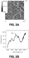
- FIG. 2A shown is an atomic force microscope (AFM) image of a CNT network with a CNT surface number density typical of that used for the source layer 113b of an embodiment of the CN-VOLET 103b.
- AFM atomic force microscope
- dilute CNT networks with about this surface number density have a very high transmittance 230, which is beneficial for allowing the light generated in the electroluminescent light emitting layer 206b of some embodiments of the CN-VOLET 103b to escape such that the energy efficiency of the CN-VOLET 103b is minimally impacted (on the order of 1%) by transmittance losses incurred by the CNT source layer 113b.
- the transmittance of the dilute network shown in FIG. 2A through the visible and near-infrared spectrum is shown in FIG. 2B and is greater than 98% in the visible wavelengths.
- the active layer 116 includes two organic semiconducting layers 203, denoted herein as 203a and 203b.
- the organic semiconducting layer 203a may include a polycrystalline organic semiconducting material, and organic semiconducting layer 203a coats at least a portion of the source layer 113 of the DS-VOLET 103.
- the coating of the source layer 113b of FIG. 1C results in a very rough top surface morphology of the organic semiconducting layer 203a due, at least in part, to the nanotubes included in the source layer 113b.
- pentacene that is grown directly onto the carbon nanotube source layer 113b nucleates polycrystalline grains that differ in orientation over the nanotubes versus the exposed CN-VOLET gate dielectric 202a adjacent to the nanotubes of the source layer 113b.
- the specific orientation of the grains nucleated on the nanotubes orients the high mobility plane of the organic semiconducting layer 203a to coincide with the direction in which current flows for operation of the CN-VOLET 103b. Therefore, the direction of the high mobility plane is highly favorable to the performance of the CN-VOLET 103b.
- the high mobility grains over the nanotubes are also the grains that grow the fastest and, therefore, the fast growing grains create high points in the final surface topology after the deposition of the organic semiconducting layer 203a.
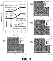
- Pentacene was grown to a thickness of 560nm at 1 ⁇ /s in a vacuum thermal evaporation chamber onto three substrate types: 1) a dilute CNT network on BCB coated glass, 2) a 45nm thick CNT film on glass and 3) a BCB coated glass substrate with no CNTs present.
- FIG. 3(a) shows an AFM image of the dilute CNT network on a BCB coated glass substrate.
- 3(b) is similar to that used in the source electrode for some embodiments of the CN-VOLET 103b.
- the lack of lower order peaks in the XRD data 233 of FIG. 3(a) for the 45nm CNT sample shows that when there are no areas of BCB exposed, there are no grains oriented with their a-b planes parallel to the surface.
- the XRD data 236 for pentacene on dilute CNT on BCB sample show XRD peaks from both grain orientations: grains with their a-b plane parallel and grains with their a-b plane near perpendicular to the substrate surface.
- the bare BCB XRD peaks in the XRD data 239 indicate only the presence of pentacene grains with their a-b planes parallel to the surface. This is indicative of the CNTs nucleating a reorientation of the pentacene grains to the near vertical direction; a direction which is favorable for charge transport in the CN-VOLET 103b enhancing its performance.
- the AFM images of FIGS. 3(c) and 3(d) of the pentacene surface of pentacene grown on a 45nm CNT film and a dilute CNT network on BCB show large root-mean-square (RMS) surface roughness values of 41.1 nm and 51.9 nm, respectively.
- RMS roughness values are significantly larger than the 20.8 nm RMS roughness measured for the pentacene on bare BCB sample AFM image in FIG. 3(e) .
- the AFM data 233, 236, and 239 show that the presence of CNTs on the substrate surface with pentacene subsequently grown on top, significantly increases the surface RMS roughness of the pentacene.
- the pentacene a-b plane is oriented in the near vertical direction the pentacene molecules are lying with their long axis parallel to the CNT long axis, as depicted in the drawing in FIG. 4
- a RMS surface roughness of >30 nm results in outliers (areas of the film of extreme highness or lowness) as high as 120 nm above and as low as 120 nm below the average thickness of the organic semiconducting layer 203a.
- These regions of the surface that protrude or descend from the average thickness of the organic semiconducting layer 203a span a range that is larger than the total thickness of all the light emitting layers 206 ( i.e ., 206a, 206b and 206c).
- This surface roughness may result in direct shorts across the light emitting layers 206, resulting in a non-operational or reduced luminance current efficiency AMDS-VOLET pixel 100.
- an amorphous, solution-processable organic semiconducting layer 203b is deposited as a planarization layer.
- the solution processable amorphous organic semiconductor poly[9,9-dioctyl-fluorene- co - N -(4-butylphenyl)-diphenylamine] (TFB) can be used for the planarization layer and serve as the organic semiconducting layer 203b.
- TFB can be spun coat from toluene or other solvents onto a rough polycrystalline small molecule organic surface. An example for such planarization by TFB of the rough polycrystalline surface is illustrated in FIG. 5.
- FIG. 5 An example for such planarization by TFB of the rough polycrystalline surface is illustrated in FIG. 5.
- FIG. 5(a) shows the rough bare polycrystalline organic surface before planarization, with a RMS surface roughness of 27 nm.
- the surface of FIG. 5(a) was made smoother than the 51.9 nm RMS surface roughness of FIG. 3(d) by modifying the growth conditions.
- FIG. 5(b) shows the same surface of FIG. 5(a) after planarization with TFB; resulting in a reduced RMS roughness of 10.5 nm.
- CN-VOLET devices 103c with the structure illustrated in FIG. 6 were fabricated with and without the TFB planarization layer and the device performance was compared.
- the substrate 126 is glass;
- the gate electrode 201a is tin doped indium oxide (ITO);
- the dielectric layer 109a is a bi-layer with first an atomic layer of deposited aluminum oxide 202a and second a layer of BCB 202d;
- the source layer 113b was a dilute CNT network with CNT surface number density similar to that shown in the AFM image of FIG.
- the first organic semiconducting layer 203a is a small molecule polycrystalline organic
- the second organic semiconducting layer 203b is TFB
- the third organic semiconducting layer 203c (the hole injection layer) is NPD co-doped with molybdenum oxide
- the hole transporting light emitting layer 206a is NPD
- the electroluminescent light emitting layer 206b is CBP co-doped with Ir(ppy)3
- the electron transporting light emitting layer 206c is 3TPYMB
- the electron injecting conducting layer 209a is lithium fluoride
- the metal conducting layer 209b is aluminum.
- the polycrystalline organic semiconductor layer 203a is shown with spikes which represent its rough surface.
- FIG. 7 illustrates the improvement in the current efficiency with a TFB planarization layer as measured in units of candelas/amp (Cd/A) and plotted as a function of the luminance of the tested CN-VOLETs 103c ( FIG. 6 ), where luminance is in units of candelas per square meter (Cd/m 2 ).
- the drain voltage (V D ) was swept from 0 V to -9 V, and the gate voltage (V G ) was held constant at -3 V. Without the TFB planarization layer, the current efficiency 243 is reduced my more than a factor of two.
- This reduction in the current efficiency is attributed to direct shorts between the first organic semiconducting layer 203a and the conducting layers 209a and 209b in the CN-VOLET device 103c without TFB resulting from the rough polycrystalline organic semiconducting layer surface.
- the CN-VOLET device 103c with TFB has more than twice the current efficiency 246 than without TFB because the organic semiconducting layers 203a and 203b together are smooth enough to allow sufficient coverage of the subsequently deposited hole injection layer 203c and light emitting layers 206a, 206b and 206c to force the current to travel through the light emitting layers 206a, 206b and 206c and therefore have a higher current efficiency.
- amorphous solution-processable organic semiconductor materials cannot match the mobility of the polycrystalline semiconductor materials.
- the fact that the high mobility orientation grains of the polycrystalline semiconductor materials are the highest features in the topography of the organic semiconducting layer 203a allows the use of a restricted thickness of the organic semiconducting layer 203b, which may fill in around the highest features while lightly coating them, thereby reducing any loss in performance due to such a layer.
- the organic semiconducting layer 203b may further be doped by a co-soluble dopant and/or interfacial dopants may be deposited before and/or after deposition of this planarization layer.
- Potential dopants include SbCl 5 , WO 3 , molybdenum oxide, ReO 3 , iron III chloride, iron oxide, 2,3,5,6-tetrafluoro-7,7,8,8-tetracyanoquinodimethane (F4TCNQ), 1,3,4,5,7,8-hexafluorotetracyanonaphthoquinodimethane (F6-TNAP) and 3,6-difluoro-2,5,7,7,8,8-hexacyanoquinodimethane (F2-HCNQ).
- the organic semiconductor layer 203a may include a doped or undoped polymer such as TFB or Poly[N,N'-bis(4-butylphenyl)-N,N'-bis(phenyl)-benzidine] (poly-TPD).
- the organic semiconductor layer 203a may include a highly conducting polymer such as poly(3,4-ethylenedioxythiophene) poly(styrene-sulfonate) (PEDOT:PSS) or a solution-deposited nanoparticle layer.
- the roughness of the planarized surface shown in FIG. 5(b) is 10.5 nm. In some applications this roughness may be too large thereby preventing high performance devices to be attained upon subsequent deposition of the light emitting layers and drain layers.
- This roughness may be reduced by spin coating a second planarization layer on top of the first. Before spin coating, the first layer is made insoluble to the second layer. One way to do this is to cross-link the first planarization layer and make it insoluble to its original solvent thereby allowing the same polymer and solvent solution to be used a second time.
- TFB is known to be cross-linkable above a certain temperature during an annealing process for an appropriate time period, which means TFB can be used as the cross-linkable first and second planarization layer, so long as it is cross-linked by the appropriate treatment prior deposition of the second TFB layer.
- the carrier mobility of TFB is lower than the polycrystalline semiconductor layer, and because of this, the use of multiple polymer planarization layers may increase the series resistance of the device increasing its power consumption more than is tolerable. Doping the polymer planarization layer is one way to alleviate this. However, with two polymer planarization layers, the second one can be more heavily doped than the first.
- the first planarization layer can be doped, because past a certain point, the on/off ratio of the DS-VOLET will begin to suffer because of an increased off-state current due to the carrier density being too high.
- the cross linking of the first polymer planarization layer will protect the more heavily doped second polymer planarization layer from contaminating the lower layers of the DS-VOLET. Having the second polymer layer doped more heavily can minimize its adverse impact on the power consumption of the DS-VOLET.
- the organic semiconductor layer 203a and light emitting layers 206a, 206b, and 206c may be deposited by thermal evaporation.
- the organic semiconducting layer 203b may be deposited by spin coating.
- a soluble high mobility wide band-gap organic small molecule may be applied in solution to serve as the organic semiconducting layer 203a by any of the below mentioned methods.
- High mobility refers to a field effect carrier mobility of about 0.01 cm 2 V -1 s -1 . With a wide-band gap, the thin film solid phase of the organic small molecule does not absorb visible light.
- the organic small molecule may form localized polycrystalline grains during and after drying of the solvent which allow it to attain a high mobility.
- the viscosity of such solutions including a dissolved organic small molecule material can be low; so low that a sufficient thickness of the material is not achievable in a spin coating or other technique as mentioned below even after increasing the concentration of the organic small molecule to the point of saturation.
- a soluble amorphous polymer such as TFB or poly-TPD may be added in a controlled amount to increase the viscosity of the soluble organic small molecule solvent solution so that it allows the chosen deposition method to achieve proper film thickness and morphology.
- a solution deposited small molecule organic semiconducting layer 203a with or without a polymer thickener may be at least as smooth as - and likely smoother than - the surface of a polymer planarized thermally evaporated small molecule organic semiconducting layer 203a.
- the organic semiconducting layer 203a can be comprised of a wide band-gap, high mobility oligomeric or polymeric material that may form localized polycrystalline grains during and after drying of the solvent through one of the below mentioned deposition methods. These localized polycrystalline grains may allow the deposited thin-film to attain high mobility.
- a solution deposited oligomeric or polymeric organic semiconducting layer 203a may be at least as smooth as - and likely smoother than - the surface of a polymer planarized thermally evaporated small molecule organic semiconducting layer 203a.
- any of the following solution processable and non-solution processable methods may be used to deposit at least one of the organic semiconducting layers 203 and the light emitting layers 206: spin-coating, dip coating, drop casting, screen printing, spray coating, vapor jet printing, physical vapor deposition, thermal gradient sublimation, doctor-blading, gravure printing, flexography, thermal evaporation and ink-jet printing.
- the conducting lines 123 including the data conducting line 123a (i.e ., providing the V data voltage signal), denoted herein as 123a1 and 123a2, source conducting line 123b ( i.e ., providing the V source voltage signal) and scan conducting line 123c ( i.e ., providing the V scan , voltage signal), may be made of at least one of the following: metal, carbon paste with or without incorporation of conducting nanoparticles, solution processable conducting polymers such as poly(3,4-ethylenedioxythiophene) poly(styrene-sulfonate) (PEDOT:PSS), solution deposited conducting nanoparticles, and pastes incorporating conducting nanoparticles.
- PEDOT:PSS poly(3,4-ethylenedioxythiophene) poly(styrene-sulfonate)
- Methods of depositing the conducting lines 123 include: sputtering, thermal evaporation, e-beam evaporation, electroplating, spin-coating, dip coating, drop casting, doctor-blading, screen printing, spray coating, gravure printing, flexography, paste deposition through a nozzle and ink-jet printing.
- a data conducting line 123a has an interlayer dielectric (ILD) between itself and the source conducting line 123b and scan conducting line 123c in the region of overlap to prevent electrical communication therebetween.
- the source conducting line 123b is in electrical contact with the source layer 113a of the DS-VOLET 103.
- the data conducting line 123a provides the connection to one side of the Sw-T 106.
- the drain layer 119 is a continuous layer along a plurality of active cells 102 in an entire column (to be described in greater detail later).
- An ILD is deposited in the region of overlap between the drain layer 119 and both the source conducting line 123b and the scan conducting line 123c.
- the ILD layer may include one or more various organic or inorganic insulating materials.
- the ILD layer may include silicon oxide, silicon nitride, aluminum oxide, hafnium oxide, BCB, or polyimide.
- the ILD layer may be deposited by PECVD, ALD, spin coating or another deposition method mentioned above.
- the switching speed of an embodiment of the CN-VOLET 103c of FIG. 6 was measured to determine if the cutoff frequency of the CN-VOLET 103c was sufficient for typical display applications.
- the pixel size was 1 mm by 1 mm - as defined by the overlap of a 1 mm wide CNT source 113b with a 1 mm wide aluminum conducting layer 209b.
- the parasitic overlap capacitance was estimated to be twice as large as the gate capacitance in the pixel because the overlap area of the CNT source layer 113b with the ITO gate electrode 201a was 1 mm (CNT width) by 3 mm (ITO width) - this gate electrode was 3 times wider than needed to aid in expedient device fabrication without much concern of layer alignment, however it may be decreased to decrease the parasitic capacitance.
- the device was given a constant voltage between the CNT source 113b and aluminum conducting layer 209b.
- the ITO gate electrode 201a was connected to a function generator supplying a square wave voltage signal, oscillating the CN-VOLET 103c between its on and off states.
- FIG. 8 shows the photodiode response 253 and input signal 256 of the CN-VOLET at a frequency of 3 kHz.
- the cutoff frequency was taken at 3 db of attenuation of the photodiode response and was measured to be about 9.1 kHz.
- Typical side dimensions of typical display pixels for hand held devices and televisions are in the range of about 100 ⁇ m to about 400 ⁇ m.
- the switching speed is inversely increased.
- the corresponding increase in switching speed for dimensional reduction of the CN-VOLET 103c ( FIG. 6 ) down to the typical hand held display and television display pixel sizes results in values of about 2.7 MHz and about 200 kHz, respectively.
- a 1920 x 1200 pixel WUXGA large screen high definition television display needs about 72 kHz for a 60 Hz screen refresh rate. Therefore it is expected that the CN-VOLET 103c has sufficient switching speed for most display applications including large size high definition television displays.
- the architecture of the DS-VOLET 103 has intrinsic benefits concerning its switching speed.
- the DS-VOLET is not governed by the same physical processes that limit the switching speed of a conventional TFT.
- the architecture of a typical TFT is such that the rate of charging and discharging of the gate charge is limited by the resistance of its channel, which when the TFT is in the off state is very high.
- the DS-VOLET however is not limited by the resistance of its channel, it is mainly limited by the resistance of the source layer 113a, which is relatively low and nearly constant whether the device is in the on or off state.
- the better agreement with the RC model is expected seeing as the charging and discharging of the CN-VOLET gate is limited by the series resistance of the source layer, which schematically is connected in series with the capacitor defined by the overlap area 218a of its gate electrode and its active area ( i.e.
- the CN-VOLET is likely to fit the parallel RC circuit model, its speed can likely be increased simply by lowering its gate capacitance by increasing the thickness or decreasing the dielectric constant of the dielectric layer 202a, which comes with the expense of a larger operating gate voltage.
- reducing the gate capacitance in an attempt to increase the cutoff frequency of a conventional TFT does not work, because of the physics involved in the governing model for TFTs, which is known by those skilled in the art.
- the AMDS-VOLET pixel 100 layout enables a larger aperture ratio for the AMDS-VOLET pixel 100 for at least the reason that the driving transistor is included in the same stack as the light emitting layers 206, which allows more area of the AMDS-VOLET pixel 100 to be devoted to emitting light.
- the capacitance between the source layer 113a and the gate electrode 201a hereby referred to as the gate capacitance, is larger than is necessary in some embodiments.
- a larger than necessary gate capacitance may limit the switching speed of the AMDS-VOLET pixel 100 and potentially limit the usefulness of the AMDS-VOLET pixel 100 in some applications.
- the gate capacitance of a DS-VOLET 103 may be decreased by using a dielectric layer 202a having a lower dielectric constant, and/or increasing the thickness of the dielectric layer 202a.
- increasing the switching speed by either of these methods comes at the expense of a proportional increase in the gate voltage.
- a proportional increase in gate voltage could potentially limit the usefulness of the AMDS-VOLET pixel 100 in some applications.
- the gate capacitance of the DS-VOLET 103 may be decreased by reducing the areal coverage on the substrate 126 of the overlapped region 218a between the gate electrode 201a and the source layer 113a, thereby reducing the gate capacitance of the DS-VOLET 103 in a manner that does not bring with it a proportional increase in gate voltage. Reducing the gate capacitance in this manner allows the switching speed of the AMDS-VOLET pixel 100 to be increased without the limiting drawbacks of a larger gate voltage. However, to maintain a large aperture ratio whilst reducing the overlap area 218a, a transitional conducting layer may be added.
- FIG. 9A shown is a cross-sectional view of another embodiment of the active cell 102 illustrated in FIG. 1A , denoted herein as 102c, that includes an example of a DS-VOLET 103, denoted herein as 103d.
- the DS-VOLET 103d illustrated in FIG. 9A differs from the DS-VOLET 103a illustrated in FIG. 1B in several ways.
- the gate electrode 201a and the source layer 113a define an overlapped region 218b, which has a smaller area than the overlapped region 218a illustrated in FIG. 1B .
- the DS-VOLET 103d further includes a transitional conducting layer 220 positioned between the light emitting layer 206 and the organic semiconductor layer 203.
- An ILD layer 223 is positioned between the transitional conducting layer 220 and the source conducting line 123b.
- FIG. 9B shown is an embodiment of an active cell, denoted as 102d, that includes an example of a CN-VOLET 103, denoted herein as 103e.
- the CN-VOLET 103e includes a dilute network of single-wall carbon nanotubes as the source layer 113b that is positioned on the CN-VOLET gate dielectric 202a over the CN-VOLET gate electrode 201a.
- the CN-VOLET 103e includes a transitional conducting layer 220 positioned between the light emitting layer 206 and the organic semiconductor layer 203.
- the transitional conducting layer 220 transfers the electrical current from the organic semiconducting layer 203, which is positioned over the source layer 113a, the gate dielectric layer 202a, and the gate electrode 201a, to the light emitting layers 206, which are deposited over a larger area, thereby allowing the light emitting region to occupy substantially all of the available area in the AMDS-VOLET pixel 100.
- the ILD layer 223 prevents electrical shorting between the source conducting line 123b and the transitional conducting layer 220.
- the transitional conducting layer 220 may include one or more layers of any conducting material such as an organic or inorganic material, a transparent or non-transparent metal, a semi-metal or semiconductor (doped or undoped, preferably doped).
- transitional conducting layer 220 includes: a single or multi-layer of graphene, a dilute network or a non-dilute layer of carbon nanotubes, tin doped indium oxide, poly(3,4-ethylenedioxythiophene) poly(styrene-sulfonate) (PEDOT:PSS), ZnO, or indium oxide nanoparticles.
- materials for the transitional conducting layer 220 include: a single or multi-layer of graphene, a dilute network or a non-dilute layer of carbon nanotubes, tin doped indium oxide, poly(3,4-ethylenedioxythiophene) poly(styrene-sulfonate) (PEDOT:PSS), ZnO, or indium oxide nanoparticles.
- the transitional conducting layer 220 is transparent to the light emitted by the light emitting layers 206.
- the transitional conducting layer 220 is a nontransparent conductor such as a metal.
- the drain layers 209 may include a transparent material, and the AMDS-VOLET pixel 100 may be included in a top light emitting display, where the light generated in the light emitting layers 206 would transmit through the transparent drain layers 209. Additionally, the reflection of light on the metallic transitional conducting layer 220 reduces light out-coupling losses of the AMDS-VOLET pixel 100.
- the top surface of the transitional conducting layer 220 could be made non-reflective and may be black in color so as to improve the contrast ratio of the AMDS-VOLET when ambient light is irradiated to the AMDS-VOLET pixel 100; this could be accomplished with a bi-layer of first a metal and then a black conductive coating such as for example: amorphous carbon, carbon nanotubes, graphene, graphite, PEDOT:PSS or C 60 .
- such an embodiment including a transitional conducting layer 220 may become particularly useful when the driving transistor layers of the DS-VOLET 103 (i.e., 201a, 202a, 113a, 203a and 203b) are sensitive to the light emitted from the light emitting layers 206, or external light encountered by the AMDS-VOLET pixel 100 in use in the environment.
- the transitional conducting layer 220 also provides a barrier to light that improves the stability of the AMDS-VOLET pixel 100.
- the areal coverage of the driving transistor layers of the DS-VOLET 103 i.e.
- 201a, 202a, 113a, 203a and 203b could be smaller than, the same as, or larger than, the areal coverage of the light emitting layers 206.
- light absorbing or reflecting layers may be added on the bottom of the substrate layer 126 or in between the gate electrode 201a and the substrate layer 126, or the substrate layer itself may be non-transparent, or the gate electrode 201a itself may include a non-transparent and/or reflecting material such as a metal for the purpose of shielding the driving transistor layers of the DS-VOLET 103 ( i.e. 201a, 202a, 113a, 203a and 203b) from light.
- inverted versions of this arrangement may be implemented without significantly deviating from the spirit of this disclosure.
- one embodiment may include a source layer 113 that injects electrons into the organic semiconducting layers 203, where the injection of these electrons may be controlled by the voltage applied to the gate electrode 201a.
- holes may be injected by the drain layer 119. These holes may then recombine with the injected electrons in the light emitting layer 206b to emit light. Additional variations include top emitting inverted designs, completely transparent noninverted and completely transparent inverted designs.
- the Sw-T 106a is a thin film transistor (TFT).
- the gate layer 109b included in the Sw-T 106a includes the Sw-T gate electrode 201b and the Sw-T gate dielectric 202b.
- the Sw-T gate electrode 201b is in direct contact with the substrate 126, and the Sw-T gate electrode 201b is in electrical contact with the scan conducting line 123c.
- the Sw-T gate dielectric 202b covers the surface of the Sw-T gate electrode 201b, as shown in the cross-sectional view in FIGS.
- the Sw-T gate dielectric 202b may be transparent or nontransparent and may include a bi-layer of an inorganic material, such as aluminum oxide, and a self assembled monolayer (SAM), such as octadecylphosphonic acid (ODPA).
- SAM self assembled monolayer
- the inorganic material provides a large capacitance, and the SAM serves as a hydrophobizing layer.
- the Sw-T 106a further includes a semiconducting layer 216 that is positioned on the Sw-T gate dielectric 202b.
- the semiconducting layer 216 may include an organic or inorganic semiconducting material (e.g ., pentacene or amorphous Si, respectively) that is transparent or nontransparent.
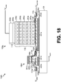
- a CN-VOLET 103c, 103f, and 103g (respectively) embodiment is shown in the cross-sectional views of various embodiments of the active cell 102 illustrated in FIGS. 6 , 13 , and 18 .
- a DS-VOLET 103 may be used instead of the CN-VOLET 103c, 103f, and 103g in the various embodiments of the active cell 102 illustrated in FIGS. 6 , 13 , and 18 .
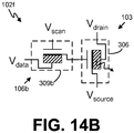
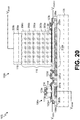
- FIG. 10 is a circuit diagram illustrating the active cell 102a shown in the cross-sectional views in FIGS. 1B , 1C , 9A , and 9B .
- the Sw-T 106a includes a thin film transistor, which is represented by a transistor circuit element 303, and the DS-VOLET 103 is represented by a DS-VOLET circuit element 306.
- the V scan signal is coupled to the gate of the transistor circuit element 303.
- the V data signal is coupled to the source/drain of the transistor circuit element 303, and the drain/source of the transistor circuit element 303 is coupled to the gate of the DS-VOLET 103.
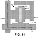
- FIG. 11 is a plan view showing an example layout of the Sw-T 106a shown in FIGS. 1B , 1C , 9A , 9B , and 3 .
- the layout shown in FIG. 11 corresponds to the Sw-T region 129 defined by dashed lines in FIG. 1A .
- the Sw-T 106a illustrated in FIG. 11 includes the gate layer 109b (including the Sw-T gate electrode 201b and the Sw-T gate dielectric 202b shown in FIGS. 1B , 1C , 9A , and 9B ), and the Sw-T 106a further includes the semiconducting layer 216 positioned on the gate layer 109b.
- the conducting line 123d is coupled to the semiconducting layer 216, and although not illustrated in FIG.
- the conducting line 123d is coupled to the DS-VOLET gate electrode 201a of the DS-VOLET 103.
- the scan conducting line 123c is coupled to the gate layer 109b, and the data conducting line 123a is coupled to the opposite end of the semiconducting layer 216 from the end of the semiconducting layer 216 coupled to the conducting line 123d.
- Sw-T designs are described including single and multiple DS-VFETs connected in various ways in place of the TFT of the embodiment described in the Sw-T 106a.
- These versions including DS-VFETs take advantage of the DS-VFET and DS-VOLET design over the traditional TFT design.
- the short channel length and large areal current capacity of the DS-VFET architecture enable the Sw-T to be made smaller for the same current output capacity and therefore occupy a smaller area than one made from a Sw-T comprising a TFT. This allows the aperture ratio of the AMDS-VOLET pixel 100 to increase further.
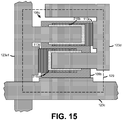
- FIG. 12 is a plan view showing an example layout of an embodiment of a Sw-T 106, denoted herein as 106b, and FIG. 13 is a cross-sectional view of an embodiment of an active cell 102e comprising the Sw-T 106b.
- the layout shown in FIG. 12 corresponds to the Sw-T region 129 defined by dashed lines in FIG. 1A .
- the Sw-T 106b includes a single carbon nanotube-enabled vertical field effect transistor (CN-VFET), which could also be replaced by a DS-VFET.
- CN-VFET carbon nanotube-enabled vertical field effect transistor
- Various embodiments of the CN-VOLET 103b, and other embodiments of the DS-VFET and DS-VOLET 103, are described in U.S.
- Patent Application Publication US 2010/0237336 having Serial No. 12/677,457 , entitled “Nanotube Enabled, Gate-Voltage Controlled Light Emitting Diodes” and filed September 10, 2008; International Publication WO 2011/109693 A2 , having International Application No. PCT/US2011/027155 , entitled “Semiconductor Devices Including an Electrically Percolating Source Layer and Methods of Fabricating the Same” and filed March 4, 2011; and U.S. Provisional Application entitled “Semiconductor Devices Including a Nanotube Layer and a Memory Layer and Methods of Fabricating the Same” having Ser. No. 61/310,342 and being filed on March 4, 2010. Unlike Sw-T 106a of FIG.
- the Sw-T 106b of FIG. 12 is a CN-VFET that includes a source layer 113c having a dilute carbon nanotube layer.
- the source layers 113b and 113c may be deposited at the same time in the case including a CN-VOLET 103f.
- the source layers 113a ( FIG. 1B ) and 113c may be deposited at the same time in the case including a DS-VOLET 103.
- the Sw-T 106b in FIGS. 12 and 13 could consist of a DS-VFET in which the source layer 113c could include others source electrodes including any of the percolating dilute networks listed earlier for the DS-VOLET 103.
- the source layer 113c can include any low density of states metal, inorganic or organic; low density of states semiconductor, inorganic or organic; or low density of states semi-metal, inorganic or organic.
- An example of a low density of states organic semi-metal includes graphene.
- Graphene can be single layered or multi-layered and can be patterned to include perforations or un-patterned. Referring to FIG. 13 , the structure of the CN-VOLET 103f is the same as the structure illustrated in the embodiment shown in FIG. 1C and could optionally be replaced by the structures shown in FIGS. 1B , 9A , or 9B .
- the Sw-T 106b illustrated in FIG. 13 includes a gate layer 109b that comprises a Sw-T gate electrode 201b and a Sw-T gate dielectric 202b.
- the Sw-T gate electrode 201b is coupled to scan conducting line 123c ( FIG. 12 ).
- the Sw-T gate dielectric 202b covers the surface of the Sw-T gate electrode 201b.
- the Sw-T gate electrode 201b may be transparent or nontransparent and may include a bi-layer of an inorganic material such as aluminum oxide (e.g., Al 2 O 3 ) and a polymer such as BCB.
- the inorganic material provides a large capacitance, and the polymer serves as a hydrophobizing layer.
- the Sw-T 106b includes a source layer 113c that is coupled to a data conducting line 123a.
- the source layer 113c includes a dilute carbon nanotube layer.
- the semiconducting layer 216 Positioned on the source layer 113c is the semiconducting layer 216.
- the semiconducting layer 216 includes a single layer or multiple layers, or doped single or multiple layers. These layers may include an organic semiconducting material, such as pentacene, or an inorganic semiconducting material, such as silicon (amorphous, nanocrystalline/microcrystalline or polycrystalline). Silicon can be deposited by PECVD.
- possible p-dopants of a semiconducting layer 116 that is organic include SbCl 5 , WO 3 , molybdenum oxide, ReO 3 , iron III chloride, iron oxide, F4-TCNQ, F2-HCNQ or F6-TNAP.
- possible dopants include boron (p-type) and phosphorous or arsenic (both n-type).
- FIG. 14A is a circuit diagram illustrating an example of the active cell 102e illustrated in FIG. 13 .
- the conducting line 123d is positioned on the semiconductor layer 216 in the Sw-T 106b to form a drain electrode coupled to a DS-VOLET 103 or to a CN-VOLET 103f.
- the Sw-T 106b includes a CN-VFET, which is represented by a CN-VFET or DS-VFET circuit element 309a in FIG. 14A .
- FIG. 14B is a circuit diagram illustrating another example of an active cell 102, denoted herein as 102f. Similar to the active cell 102e illustrated in FIG.
- the active cell 102f includes a DS-VOLET 103.
- the active cell 102f also includes a Sw-T 106b.
- the Sw-T 106b includes a CN-VFET, which is represented by a CN-VFET or DS-VFET circuit element 309b in FIG. 14B .
- the source-drain connections of the Sw-T 106b are reversed.
- the source electrode (i.e., the source layer 113c) of the Sw-T 106b (instead of the drain electrode of the Sw-T 106b) is coupled to the conducting line 123d allowing electrical connection to the gate electrode 201a of the CN-VOLET 103. Accordingly, in the active cell 102f, the drain electrode is formed by the data conducting line 123a1.
- FIG. 15 is a plan view showing an example layout of an embodiment of a Sw-T 106, denoted herein as 106c
- FIG. 16 is a circuit diagram including an embodiment of an active cell 102g comprising the Sw-T 106c illustrated in the plan view shown in FIG. 15 .
- the layout shown in FIG. 15 corresponds to the Sw-T region 129 defined by dashed lines in FIG. 1A .
- the Sw-T 106c shown includes a double lateral CN-VFET or a double lateral DS-VFET.
- FIG. 15 is a plan view showing an example layout of an embodiment of a Sw-T 106, denoted herein as 106c
- FIG. 16 is a circuit diagram including an embodiment of an active cell 102g comprising the Sw-T 106c illustrated in the plan view shown in FIG. 15 .
- the layout shown in FIG. 15 corresponds to the Sw-T region 129 defined by dashed lines in FIG. 1A .
- the double lateral CN-VFET or double lateral DS-VFET included in the Sw-T 106c is represented by a double lateral CN-VFET or double lateral DS-VFET circuit element 312.
- a double lateral CN-VFET includes two CN-VFETs coupled in parallel and positioned side-by-side with reversed source layers 113c, 113d and drain electrodes, and the two CN-VFETs share a common gate layer 109b.
- a double lateral DS-VFET includes two DS-VFETs coupled in parallel and positioned side-by-side with reversed source layers 113c, 113d and drain electrodes, and the two DS-VFETs share a common gate layer 109b.
- the Sw-T 106c (i.e ., including a double lateral CN-VFET or double lateral DS-VFET) enables better current control than the Sw-T 106b over supplying and removing charge to and from the DS-VOLET gate electrode 201a from the data conducting line 123a.
- the Sw-T 106b i.e., including the single CN-VFET or DS-VFET of FIGS.
- the current travels from the source layer 113c to the conducting line 123d ( i.e., from source to drain), and the current is sufficiently controlled to add an adequate amount of charge to operate the DS-VOLET 103 at a specified gray scale.
- the Sw-T 106b is reverse biased, the current traveling from the conducting line 123d to the source layer 113c ( i.e., from drain to source) is not sufficiently controlled, resulting in a loss of the charge stored on the DS-VOLET gate electrode 201a in the time between refresh events of the active cell 102.
- a refresh event includes an addressing of the active cell 102 by pulsing the voltage of the scan conducting line 123c of a specified row, thereby charging the DS-VOLET gate electrode 201a of the DS-VOLET 103 with a charge from the data conducting line 123a of a specified column. Controlling the traveling of the charge equally well to and from the gate of the DS-VOLET 103 provides for successful operation of the AMDS-VOLET pixel 100.
- the gate layer 109b, source layers 113c, 113d, semiconductor layers 216b, 216c of the double lateral CN-VFET or double lateral DS-VFET included in the Sw-T 106c may be made using the same fabrication processes as the Sw-T 106b mentioned above, except that the layers of the Sw-T 106c are patterned as illustrated in the example layout shown in FIG. 15 . Additionally, the source layers 113c, 113d may be deposited at the same time as part of the same patterned layer. Likewise, the semiconductor layers 216b, 216c may also be deposited at the same time as part of the same patterned layer. The arrangement of these layers is shown in the example illustrated in FIG. 15 .
- the conducting line 123d, forming the drain electrode of the lower single CN-VFET or DS-VFET in FIG. 15 may include a material that forms a Schottky barrier > 0.1 eV for electrons or holes when in contact with the semiconductor layers 216b, 216c of the double lateral CN-VFET or double lateral DS-VFET.
- FIG. 17 is a plan view showing an example layout of another embodiment of a Sw-T 106, denoted herein as 106d
- FIG. 18 is a cross-sectional view of an embodiment of an active cell 102h comprising the Sw-T 106d.
- the layout shown in FIG. 17 corresponds to the Sw-T region 129 defined by dashed lines in FIG. 1A .
- the Sw-T 106d comprises a double inverted CN-VFET or double inverted DS-VFET.
- Pictured in FIG. 18 is an embodiment of the Sw-T 106d comprising a double inverted CN-VFET.
- the double inverted CN-VFET and double inverted DS-VFET have a design similar to a single CN-VFET and DS-VFET, respectively, with at least one difference being the addition of another source layer 113e that functions as a drain layer.
- the source layer 113e includes a dilute carbon nanotube network in the case when the Sw-T 106d comprises a double inverted CN-VFET, and the source layer 113e is coupled to the conducting line 123d.
- a gate layer 109c is positioned on the source layer 113e including a Sw-T gate dielectric 202c and a Sw-T gate electrode 201c, as shown in FIGS. 17 and 18 .
- the gate layer 109b, the source layer 113c, the semiconductor layer 216 of the double inverted CN-VFET or double inverted DS-VFET may be made in the same manner and from the same materials as the Sw-T 106b mentioned above, except that the layers of the Sw-T 106d are patterned as illustrated in the example layout shown in FIG. 17 .
- the coverage of the layers is shown in the examples illustrated in FIG. 17 and 18 .
- the source layer 113e is deposited on the semiconductor layer 216, and a second gate layer 109c is deposited on the source layer 113e. As shown in FIG.
- the second gate layer 109c includes a Sw-T gate dielectric 202c deposited on the source layer 113e and a Sw-T gate electrode 201c deposited on the Sw-T gate dielectric 202c.
- the Sw-T gate dielectric 202c may be a single insulating layer or multiple insulating layers.
- the Sw-T gate electrode 201c may be a metal (e.g., aluminum (Al)), a TCO (e.g., ITO), and/or a mixture of the two or other conducting materials including carbon nanotubes, graphene, PEDOT:PSS and conductive nanoparticles.
- FIG. 19 is a plan view showing an example layout of another embodiment of a Sw-T 106, denoted herein as 106e
- FIG. 20 is a cross-sectional view of an embodiment of an active cell 102j comprising the Sw-T 106e.
- the layout shown in FIG. 19 corresponds to the Sw-T region 129 defined by dashed lines in FIG. 1A .
- the Sw-T 106e comprises a reversed series double CN-VFET or reversed series double DS-VFET.
- Pictured in FIGS. 19 and 20 is the embodiment of the Sw-T 106e comprising a reversed series double DS-VFET.
- the reversed series double DS-VFET has a design similar to a single DS-VFET, with at least one difference being the addition of another source layer 113f that functions as the source layer of a second series connected, but reversed in polarity, DS-VFET.
- the source layer 113f includes all the previously mentioned materials for the DS-VFET or DS-VOLET including a dilute nanotube network.
- the source layer 113f is coupled to the conducting line 123d.
- the drain electrode 123e of the Sw-T 106e is shared between both DS-VFETs as shown in FIGS. 19 and 20 .
- FIG. 21 shows a circuit diagram for the active cell 102j including a reversed series double DS-VFET Sw-T 106e which is denoted as circuit element 313.
- the gate layer 109b, the source layers 113f and 113g, the semiconductor layer 216 of the reversed series double DS-VFET may be made in the same manner and from the same materials as the Sw-T 106b mentioned above, except that the layers of the Sw-T 106e are patterned as illustrated in the example layout shown in FIGS. 19 and 20 .
- the drain electrode 123e may include a material that forms an ohmic contact barrier ⁇ 0.2 eV for electrons or holes when in contact with the semiconductor layer 216b of the reversed series double DS-VFET.
- FIG. 23 is a cross-sectional view of an embodiment of an active cell 102k comprising the Sw-T 106f.
- the DS-VFETs in the Sw-T 106f share a common source electrode 113h with separately patterned drain electrodes as shown in FIGS. 22 and 23 .
- FIG. 24 shows a circuit diagram for the reversed series double DS-VFET Sw-T 106f with its circuit element denoted as 314.
- FIG. 25 is a plan view showing an example layout of embodiment of an array 1200 of AMDS-VOLET pixels 100, denoted herein as 1200a.
- Each AMDS-VOLET pixel 100 each emits light of the same color, and each AMDS-VOLET pixel 100 includes an active cell 102 according to any of the embodiments described above.
- the active cells 102 are laid out in an array 1200a of n columns by m rows, with the location of each active cell 102 designated by coordinates (n,m), where n is the column number and m is the row number.
- Each active cell 102 is addressable by the V scan-n and V data-m signals which are provided by external control circuitry, which may be mounted to a display panel in its periphery.
- the V drain-m voltage signals may all be connected to a single voltage supply providing a specified voltage.
- the V source voltage signals may all be connected to a single voltage supply providing a specified voltage.
- FIG. 26 is a plan view showing an example layout of another embodiment of an array 1200 of AMDS-VOLET pixels 100, denoted herein as 1200b.
- Each AMDS-VOLET pixel 100 includes three active cells 102, each emitting a different color (e.g., red, blue, green), according to any of the embodiments described above.
- the AMDS-VOLET pixel 100 includes three active cells 102 side-by-side, where one active cell 102 is red (R), one green (G), and the other blue (B).
- Repeated active cells 102 are laid out in a matrix of n columns by m rows, with the location of each repeated cell designated by coordinates, (n,m), where n is the column number and m is the row number.
- Each column Cn is divided into three colors as shown in FIG. 26 .
- Column Cn is divided into individual columns according to the column color ( e.g., Rn (red), Gn (green) and Bn (blue)).
- the various colors of the active cells 102 may be achieved according to various color attainment methods.
- the color is determined by the choice of material used in the light emitting layer 206b (i.e., the EL layer) of the DS-VOLET 103 in the respective active cell 102.
- the material included in the light emitting layer 206b emits the desired color, either R, G, or B.
- the material included in the light emitting layer 206b is chosen to emit white light and an appropriate color filter layer is employed to allow the specified R, G or B color to transmit through the color filter layer.
- the color filter layer may be placed on the opposite side of the substrate layer 126 or between the substrate layer 126 and the gate layer 109a in the area where the specified color is desired (e.g., in a bottom emission display where light from the light emitting layer 206b is emitted through the substrate layer 126).
- the color filter layer may be placed on top of the drain layer(s) 119.
- the light emitting layer 206b emits blue light and an appropriate color change layer is employed to attain R and G light on the R and G active cells, respectively.
- the position of the color change layer may be similar to that used for the color filter layer in the second color attainment method.
- Photolithography is a widely used method that is used for defining patterns for subsequent process steps such as subtractive etching (either wet or dry) of the material of interest which was deposited over the entire substrate prior to deposition of the photoresist.
- Photoresist is the polymer material used for making patterns by exposing desired regions with, typically, ultraviolet (UV) light. The exposed/unexposed regions of the positive/negative photoresist become soluble in developer solution after UV light exposure.
- the photoresist also covers the entire substrate and is typically deposited by spin coating. Methods other than subtractive etching may be utilized as well.
- Methods such as the lift-off process may also be used for other material types.
- the photoresist is applied prior to the deposition of the material of interest, which may be, for example, a metal.
- the photoresist which is typically specifically designed for this purpose, typically referred to as a lift-off resist, then undergoes the conventional photolithography process steps of, UV light exposure and pattern development in developer solution.
- the metal may be deposited by a conventional method, such as sputtering.
- the regions where the lift-off resist is still present may be dissolved in a solvent, and the metal may be lifted off in those regions, leaving behind a patterned metal layer with the desired layout.
- methods that are self patterning such as gravure printing, flexography, ink-jet printing and vapor jet printing, conventional photolithography may not be necessary.
- organic semiconducting layers are not necessarily restricted to being organic.
- the organic semiconducting layers may be inorganic, in which case they would be merely semiconducting layers.
- Possible inorganic semiconductors include silicon (amorphous, single crystal, micro/nanocrystalline and polycrystalline) and nanoparticles.
- ratios, concentrations, amounts, and other numerical data may be expressed herein in a range format. It is to be understood that such a range format is used for convenience and brevity, and thus, should be interpreted in a flexible manner to include not only the numerical values explicitly recited as the limits of the range, but also to include all the individual numerical values or sub-ranges encompassed within that range as if each numerical value and sub-range is explicitly recited.
Landscapes
- Engineering & Computer Science (AREA)
- Chemical & Material Sciences (AREA)
- Materials Engineering (AREA)
- Physics & Mathematics (AREA)
- Microelectronics & Electronic Packaging (AREA)
- Optics & Photonics (AREA)
- Nanotechnology (AREA)
- Geometry (AREA)
- Manufacturing & Machinery (AREA)
- Thin Film Transistor (AREA)
- Electroluminescent Light Sources (AREA)
- Control Of Indicators Other Than Cathode Ray Tubes (AREA)
- Electrodes Of Semiconductors (AREA)
Applications Claiming Priority (2)
| Application Number | Priority Date | Filing Date | Title |
|---|---|---|---|
| US42051210P | 2010-12-07 | 2010-12-07 | |
| PCT/US2011/063745 WO2012078759A2 (en) | 2010-12-07 | 2011-12-07 | Active matrix dilute source enabled vertical organic light emitting transistor |
Publications (3)
| Publication Number | Publication Date |
|---|---|
| EP2649659A2 EP2649659A2 (en) | 2013-10-16 |
| EP2649659A4 EP2649659A4 (en) | 2015-01-07 |
| EP2649659B1 true EP2649659B1 (en) | 2020-05-06 |
Family
ID=46207712
Family Applications (1)
| Application Number | Title | Priority Date | Filing Date |
|---|---|---|---|
| EP11846649.9A Active EP2649659B1 (en) | 2010-12-07 | 2011-12-07 | Active matrix display comprising a dilute source enabled vertical organic light emitting transistor |
Country Status (12)
Families Citing this family (54)
| Publication number | Priority date | Publication date | Assignee | Title |
|---|---|---|---|---|
| US9412442B2 (en) * | 2012-04-27 | 2016-08-09 | The Board Of Trustees Of The University Of Illinois | Methods for forming a nanowire and apparatus thereof |
| US8901547B2 (en) * | 2012-08-25 | 2014-12-02 | Polyera Corporation | Stacked structure organic light-emitting transistors |
| US8653516B1 (en) * | 2012-08-31 | 2014-02-18 | Eastman Kodak Company | High performance thin film transistor |
| TWI569491B (zh) * | 2012-10-11 | 2017-02-01 | Joled Inc | Organic EL display device and manufacturing method thereof, ink and electronic machine |
| TWI467301B (zh) * | 2012-10-24 | 2015-01-01 | Au Optronics Corp | 顯示面板 |
| WO2014071343A1 (en) * | 2012-11-05 | 2014-05-08 | University Of Florida Research Foundation, Inc. | Brightness compensation in a display |
| KR102010113B1 (ko) * | 2012-11-30 | 2019-08-12 | 유니버시티 오브 플로리다 리서치 파운데이션, 아이엔씨. | 양극성 수직 전계 효과 트랜지스터 |
| KR102081891B1 (ko) * | 2013-02-15 | 2020-02-26 | 삼성전자주식회사 | 그래핀 소자 및 이를 포함하는 전자 기기 |
| US9373685B2 (en) * | 2013-02-15 | 2016-06-21 | Samsung Electronics Co., Ltd. | Graphene device and electronic apparatus |
| US8975121B2 (en) * | 2013-05-09 | 2015-03-10 | Johnson & Johnson Vision Care, Inc. | Methods and apparatus to form thin film nanocrystal integrated circuits on ophthalmic devices |
| CN104576744A (zh) * | 2013-10-24 | 2015-04-29 | 中国科学院苏州纳米技术与纳米仿生研究所 | 碳纳米管薄膜晶体管、amoled像素柔性驱动电路及制作方法 |
| GB201321285D0 (en) | 2013-12-03 | 2014-01-15 | Plastic Logic Ltd | Pixel driver circuit |
| IL229837A0 (en) | 2013-12-08 | 2014-03-31 | Technion Res & Dev Foundation | Electronic device |
| KR102445520B1 (ko) | 2014-04-24 | 2022-09-20 | 유니버시티 오브 플로리다 리서치 파운데이션, 인크. | 고전력 전자기기를 위한 조정 가능한 배리어 트랜지스터 |
| KR102237826B1 (ko) * | 2014-07-18 | 2021-04-08 | 삼성전자주식회사 | 그래핀 소자와 그 제조 및 동작방법과 그래핀 소자를 포함하는 전자장치 |
| EP2978038A1 (en) * | 2014-07-24 | 2016-01-27 | E.T.C. S.r.l. | Organic electroluminescent transistor |
| JP6612236B2 (ja) * | 2014-09-04 | 2019-11-27 | 株式会社Joled | 表示装置および電子機器 |
| US9379166B2 (en) * | 2014-11-04 | 2016-06-28 | Atom Nanoelectronics, Inc. | Active matrix light emitting diodes display module with carbon nanotubes control circuits and methods of fabrication |
| EP3021373A1 (en) | 2014-11-14 | 2016-05-18 | E.T.C. S.r.l. | Display containing improved pixel architectures |
| CN105679949A (zh) * | 2014-12-04 | 2016-06-15 | 广州华睿光电材料有限公司 | 有机发光晶体管及其应用 |
| US10651407B2 (en) | 2015-09-11 | 2020-05-12 | Nanoholdings, Llc | Vertical field-effect transistor |
| US10483325B2 (en) | 2015-09-11 | 2019-11-19 | University Of Florida Research Foundation, Incorporated | Light emitting phototransistor |
| CN105304830A (zh) * | 2015-10-09 | 2016-02-03 | Tcl集团股份有限公司 | 量子点发光场效应晶体管及其制备方法 |
| CN105355799A (zh) * | 2015-10-12 | 2016-02-24 | Tcl集团股份有限公司 | 一种量子点发光场效应晶体管及其制备方法 |
| KR101730902B1 (ko) * | 2015-10-19 | 2017-04-27 | 서울대학교산학협력단 | 누설 전류가 저감된 수직형 유기 발광 트랜지스터 및 이의 제조 방법 |
| WO2017112932A1 (en) * | 2015-12-23 | 2017-06-29 | University Of Florida Research Foundation, Incorporated | Patterning and inverted deposition engineering for solution-processed electrodes and semiconducting films |
| KR20170129983A (ko) | 2016-05-17 | 2017-11-28 | 삼성전자주식회사 | 발광소자 패키지, 이를 이용한 디스플레이 장치 및 그 제조방법 |
| CN106684251B (zh) * | 2016-12-09 | 2018-06-01 | 武汉华星光电技术有限公司 | 柔性垂直沟道有机薄膜晶体管及其制作方法 |
| RU175418U1 (ru) * | 2016-12-12 | 2017-12-04 | Российская Федерация, от имени которой выступает федеральное государственное казенное учреждение "Войсковая часть 68240" (ФГКУ "В/ч" 68240) | Полевой транзистор на углеродной пленке с вертикальным каналом проводимости |
| CN107170748B (zh) * | 2017-04-20 | 2019-11-08 | 上海天马微电子有限公司 | 一种阵列基板、显示面板及显示设备 |
| JP6844845B2 (ja) | 2017-05-31 | 2021-03-17 | 三国電子有限会社 | 表示装置 |
| CN108731855B (zh) * | 2018-05-18 | 2019-07-26 | 京东方科技集团股份有限公司 | 一种压力传感单元及压力传感器、压力传感装置 |
| CN108493229A (zh) * | 2018-05-31 | 2018-09-04 | 京东方科技集团股份有限公司 | 显示基板及其制备方法、显示装置 |
| JP7190729B2 (ja) * | 2018-08-31 | 2022-12-16 | 三国電子有限会社 | キャリア注入量制御電極を有する有機エレクトロルミネセンス素子 |
| KR102135503B1 (ko) | 2018-09-06 | 2020-07-17 | 광운대학교 산학협력단 | 저차원 전자구조의 물질로 구성되는 전극을 사용하는 유기 트랜지스터 소자와 유기 발광 트랜지스터 소자 및 그 제조방법 |
| CN109036283B (zh) * | 2018-09-06 | 2020-06-09 | 京东方科技集团股份有限公司 | 有机发光场效应晶体管的驱动电路及驱动方法、显示装置 |
| JP7246681B2 (ja) | 2018-09-26 | 2023-03-28 | 三国電子有限会社 | トランジスタ及びトランジスタの製造方法、並びにトランジスタを含む表示装置 |
| JP7565150B2 (ja) * | 2019-04-26 | 2024-10-10 | Jsr株式会社 | ディスプレイの輝度補償方法及びディスプレイ |
| WO2020218421A1 (en) * | 2019-04-26 | 2020-10-29 | Jsr Corporation | Method of compensating brightness of display and display |
| JP2020183971A (ja) * | 2019-04-26 | 2020-11-12 | Jsr株式会社 | ディスプレイの点灯方法及びディスプレイ |
| US12027118B2 (en) | 2019-04-26 | 2024-07-02 | Jsr Corporation | Method of driving a light emitting display and display |
| KR102825031B1 (ko) * | 2019-11-27 | 2025-06-24 | 삼성전자주식회사 | 표시 패널 및 표시 장치 |
| JP7444436B2 (ja) | 2020-02-05 | 2024-03-06 | 三国電子有限会社 | 液晶表示装置 |
| KR20220137905A (ko) | 2020-02-07 | 2022-10-12 | 제이에스알 가부시끼가이샤 | 디스플레이 |
| JP7591196B2 (ja) * | 2020-02-07 | 2024-11-28 | Jsr株式会社 | ディスプレイ |
| CN111863892B (zh) * | 2020-07-13 | 2022-08-23 | 武汉华星光电半导体显示技术有限公司 | 显示装置及其制备方法 |
| JP7367635B2 (ja) * | 2020-08-21 | 2023-10-24 | Jsr株式会社 | ディスプレイ |
| US11963413B2 (en) | 2020-08-21 | 2024-04-16 | Jsr Corporation | Display |
| RU204091U1 (ru) * | 2020-12-25 | 2021-05-06 | Общество с ограниченной ответственностью "Сенсор Микрон" | Полевой транзистор с вертикальным каналом для СВЧ - техники |
| TW202232461A (zh) | 2021-02-03 | 2022-08-16 | 日商Jsr股份有限公司 | 顯示器的製造方法及顯示器 |
| CN113345967B (zh) * | 2021-05-21 | 2022-09-09 | Tcl华星光电技术有限公司 | 薄膜晶体管及led背板 |
| WO2023115553A1 (en) * | 2021-12-24 | 2023-06-29 | Boe Technology Group Co., Ltd. | Array substrate and display apparatus |
| US20230403918A1 (en) * | 2022-06-09 | 2023-12-14 | Jsr Corporation | Method for producing vertical organic light-emitting transistor device, display |
| WO2025122930A1 (en) * | 2023-12-06 | 2025-06-12 | Mattrix Technologies, Inc. | Hybrid active-passive matrix devices for displays, lighting and signaling |
Citations (1)
| Publication number | Priority date | Publication date | Assignee | Title |
|---|---|---|---|---|
| US20100244710A1 (en) * | 2006-01-30 | 2010-09-30 | Katsunari Obata | Organic Luminescence Transistor Device and Manufacturing Method Thereof |
Family Cites Families (22)
| Publication number | Priority date | Publication date | Assignee | Title |
|---|---|---|---|---|
| FI107109B (fi) | 1998-10-21 | 2001-05-31 | Nokia Networks Oy | Digitaalinen tietoliikennejärjestelmä |
| KR100379566B1 (ko) * | 2000-08-30 | 2003-04-10 | 엘지.필립스 엘시디 주식회사 | 액정표시장치 제조방법 |
| JP3638922B2 (ja) | 2001-07-17 | 2005-04-13 | 株式会社半導体エネルギー研究所 | 発光装置 |
| GB0130321D0 (en) * | 2001-12-19 | 2002-02-06 | Avecia Ltd | Electronic devices |
| JP2003330412A (ja) | 2002-05-10 | 2003-11-19 | Canon Inc | アクティブマトリックス型ディスプレイ及びスイッチ回路 |
| US7002302B2 (en) * | 2002-10-07 | 2006-02-21 | Samsung Sdi Co., Ltd. | Flat panel display |
| JP2005128310A (ja) * | 2003-10-24 | 2005-05-19 | Seiko Epson Corp | 表示装置、及び電子機器 |
| KR100603334B1 (ko) * | 2004-04-06 | 2006-07-20 | 삼성에스디아이 주식회사 | 능동형 유기 el 픽셀 |
| TWI405242B (zh) * | 2004-04-28 | 2013-08-11 | Semiconductor Energy Lab | 基板上配線,半導體裝置及其製造方法 |
| US7416924B2 (en) * | 2004-11-11 | 2008-08-26 | Samsung Electronics Co., Ltd. | Organic light emitting display with single crystalline silicon TFT and method of fabricating the same |
| KR100634543B1 (ko) * | 2005-04-16 | 2006-10-13 | 삼성전자주식회사 | 단결정 실리콘 tft 유기발광 디스플레이 및 그 제조방법 |
| KR100712111B1 (ko) * | 2004-12-14 | 2007-04-27 | 삼성에스디아이 주식회사 | 보조 전극 라인을 구비하는 유기전계발광소자 및 그의제조 방법 |
| EP2264690A1 (en) * | 2005-05-02 | 2010-12-22 | Semiconductor Energy Laboratory Co, Ltd. | Display device and gray scale driving method with subframes thereof |
| JP4808479B2 (ja) * | 2005-11-28 | 2011-11-02 | 大日本印刷株式会社 | 有機発光トランジスタ素子及びその製造方法並びに発光表示装置 |
| US8232561B2 (en) | 2006-06-29 | 2012-07-31 | University Of Florida Research Foundation, Inc. | Nanotube enabled, gate-voltage controlled light emitting diodes |
| TWI425693B (zh) * | 2008-03-14 | 2014-02-01 | Univ Nat Chiao Tung | Vertical drive and parallel drive organic light emitting crystal structure |
| TWI637444B (zh) * | 2008-08-08 | 2018-10-01 | 半導體能源研究所股份有限公司 | 半導體裝置的製造方法 |
| KR101097454B1 (ko) * | 2009-02-16 | 2011-12-23 | 네오뷰코오롱 주식회사 | Oled 패널의 화소 회로, 이를 이용한 표시 장치 및 oled 패널의 구동 방법 |
| WO2010135539A1 (en) * | 2009-05-20 | 2010-11-25 | The Trustees Of The University Of Pennsylvania | Self-adaptive bio-signal and modulation device |
| CN101615613B (zh) * | 2009-08-12 | 2010-10-06 | 友达光电股份有限公司 | 像素结构、有机电激发光显示单元及其制造方法 |
| KR20110058126A (ko) * | 2009-11-25 | 2011-06-01 | 삼성모바일디스플레이주식회사 | 유기 발광 표시 장치 |
| JP5810103B2 (ja) | 2010-03-04 | 2015-11-11 | ユニバーシティ オブ フロリダ リサーチ ファンデーション インコーポレーティッド | 電気的浸透性ソース層を含む半導体デバイス及びこれの製造方法 |
-
2011
- 2011-12-07 JP JP2013543313A patent/JP6272030B2/ja active Active
- 2011-12-07 CA CA2820256A patent/CA2820256A1/en not_active Abandoned
- 2011-12-07 EP EP11846649.9A patent/EP2649659B1/en active Active
- 2011-12-07 BR BR112013013873A patent/BR112013013873A2/pt not_active IP Right Cessation
- 2011-12-07 RU RU2013131102/28A patent/RU2013131102A/ru not_active Application Discontinuation
- 2011-12-07 AU AU2011338460A patent/AU2011338460A1/en not_active Withdrawn
- 2011-12-07 CN CN201180064181.9A patent/CN103460424B/zh active Active
- 2011-12-07 KR KR1020137017559A patent/KR101943595B1/ko active Active
- 2011-12-07 CN CN201610835745.9A patent/CN106887449B/zh active Active
- 2011-12-07 MX MX2013006233A patent/MX2013006233A/es unknown
- 2011-12-07 US US13/519,176 patent/US9214644B2/en active Active
- 2011-12-07 WO PCT/US2011/063745 patent/WO2012078759A2/en active Application Filing
- 2011-12-07 SG SG2013037866A patent/SG190313A1/en unknown
Patent Citations (1)
| Publication number | Priority date | Publication date | Assignee | Title |
|---|---|---|---|---|
| US20100244710A1 (en) * | 2006-01-30 | 2010-09-30 | Katsunari Obata | Organic Luminescence Transistor Device and Manufacturing Method Thereof |
Also Published As
| Publication number | Publication date |
|---|---|
| EP2649659A2 (en) | 2013-10-16 |
| MX2013006233A (es) | 2013-08-15 |
| RU2013131102A (ru) | 2015-01-20 |
| JP2014505324A (ja) | 2014-02-27 |
| AU2011338460A1 (en) | 2013-06-06 |
| CN106887449B (zh) | 2021-11-05 |
| BR112013013873A2 (pt) | 2016-09-13 |
| CN103460424B (zh) | 2016-10-26 |
| WO2012078759A3 (en) | 2012-09-27 |
| US20130240842A1 (en) | 2013-09-19 |
| EP2649659A4 (en) | 2015-01-07 |
| CN103460424A (zh) | 2013-12-18 |
| CN106887449A (zh) | 2017-06-23 |
| CA2820256A1 (en) | 2012-06-14 |
| WO2012078759A2 (en) | 2012-06-14 |
| SG190313A1 (en) | 2013-06-28 |
| JP6272030B2 (ja) | 2018-01-31 |
| KR101943595B1 (ko) | 2019-04-17 |
| KR20130130011A (ko) | 2013-11-29 |
| US9214644B2 (en) | 2015-12-15 |
Similar Documents
| Publication | Publication Date | Title |
|---|---|---|
| EP2649659B1 (en) | Active matrix display comprising a dilute source enabled vertical organic light emitting transistor | |
| US11177465B2 (en) | Devices, structures, materials and methods for vertical light emitting transistors and light emitting displays | |
| JP4885462B2 (ja) | ドナーシート、ドナーシートの製造方法、ドナーシートを利用した薄膜トランジスタの製造方法、及びドナーシートを利用した平板表示装置の製造方法 | |
| KR101497744B1 (ko) | 나노튜브 가능한, 게이트 전압이 제어된 발광 다이오드 | |
| KR100994677B1 (ko) | 발광 소자 및 그 제조 방법 | |
| US7812342B2 (en) | Thin film transistor having a nano semiconductor sheet and method of manufacturing the same | |
| US8933450B2 (en) | Organic electro-luminescent display device | |
| US11152587B2 (en) | Light transmissive electrode for light emitting devices | |
| JP4476867B2 (ja) | 薄膜トランジスタ,電子装置およびフラットパネルディスプレイ装置 | |
| KR100647599B1 (ko) | 유기 전계 발광 표시장치 및 그 제조 방법 | |
| TW200529695A (en) | Organic electroluminescence display device and its fabrication method | |
| US8124963B2 (en) | Thin film transistor, method of fabricating the thin film transistor, organic light emitting diode display device, method of fabricating the organic light emitting diode display device, and donor substrate for laser induced thermal imaging | |
| KR100625994B1 (ko) | 유기 전계 발광 표시장치 및 그 제조 방법 | |
| JP2012144456A (ja) | 有機薄膜、有機薄膜の製造方法、電界効果トランジスタ、有機発光素子、太陽電池、表示装置用アレイ及び表示装置 | |
| KR100615290B1 (ko) | 평판표시장치 | |
| CN116761486A (zh) | 一种石墨烯像素电极限域载流子传输及其柔性有源矩阵发光二极管的制备方法 | |
| Bade | Fully Printable Single Layer Halide Perovskite/Peo Composite Thin Film LEDs |
Legal Events
| Date | Code | Title | Description |
|---|---|---|---|
| PUAI | Public reference made under article 153(3) epc to a published international application that has entered the european phase |
Free format text: ORIGINAL CODE: 0009012 |
|
| 17P | Request for examination filed |
Effective date: 20130705 |
|
| AK | Designated contracting states |
Kind code of ref document: A2 Designated state(s): AL AT BE BG CH CY CZ DE DK EE ES FI FR GB GR HR HU IE IS IT LI LT LU LV MC MK MT NL NO PL PT RO RS SE SI SK SM TR |
|
| RIN1 | Information on inventor provided before grant (corrected) |
Inventor name: MCCARTHY, MITCHELL, AUSTIN Inventor name: RINZLER, ANDREW, GABRIEL Inventor name: LIU, BO |
|
| RAP1 | Party data changed (applicant data changed or rights of an application transferred) |
Owner name: UNIVERSITY OF FLORIDA RESEARCH FOUNDATION, INC. |
|
| DAX | Request for extension of the european patent (deleted) | ||
| A4 | Supplementary search report drawn up and despatched |
Effective date: 20141204 |
|
| RIC1 | Information provided on ipc code assigned before grant |
Ipc: H01L 29/786 20060101ALI20141128BHEP Ipc: H01L 51/10 20060101AFI20141128BHEP Ipc: H01L 51/52 20060101ALI20141128BHEP |
|
| STAA | Information on the status of an ep patent application or granted ep patent |
Free format text: STATUS: EXAMINATION IS IN PROGRESS |
|
| 17Q | First examination report despatched |
Effective date: 20170719 |
|
| GRAP | Despatch of communication of intention to grant a patent |
Free format text: ORIGINAL CODE: EPIDOSNIGR1 |
|
| STAA | Information on the status of an ep patent application or granted ep patent |
Free format text: STATUS: GRANT OF PATENT IS INTENDED |
|
| INTG | Intention to grant announced |
Effective date: 20191122 |
|
| GRAS | Grant fee paid |
Free format text: ORIGINAL CODE: EPIDOSNIGR3 |
|
| GRAA | (expected) grant |
Free format text: ORIGINAL CODE: 0009210 |
|
| STAA | Information on the status of an ep patent application or granted ep patent |
Free format text: STATUS: THE PATENT HAS BEEN GRANTED |
|
| AK | Designated contracting states |
Kind code of ref document: B1 Designated state(s): AL AT BE BG CH CY CZ DE DK EE ES FI FR GB GR HR HU IE IS IT LI LT LU LV MC MK MT NL NO PL PT RO RS SE SI SK SM TR |
|
| REG | Reference to a national code |
Ref country code: GB Ref legal event code: FG4D |
|
| REG | Reference to a national code |
Ref country code: AT Ref legal event code: REF Ref document number: 1268257 Country of ref document: AT Kind code of ref document: T Effective date: 20200515 Ref country code: CH Ref legal event code: EP |
|
| REG | Reference to a national code |
Ref country code: IE Ref legal event code: FG4D |
|
| REG | Reference to a national code |
Ref country code: DE Ref legal event code: R096 Ref document number: 602011066764 Country of ref document: DE |
|
| REG | Reference to a national code |
Ref country code: LT Ref legal event code: MG4D |
|
| REG | Reference to a national code |
Ref country code: NL Ref legal event code: MP Effective date: 20200506 |
|
| PG25 | Lapsed in a contracting state [announced via postgrant information from national office to epo] |
Ref country code: LT Free format text: LAPSE BECAUSE OF FAILURE TO SUBMIT A TRANSLATION OF THE DESCRIPTION OR TO PAY THE FEE WITHIN THE PRESCRIBED TIME-LIMIT Effective date: 20200506 Ref country code: GR Free format text: LAPSE BECAUSE OF FAILURE TO SUBMIT A TRANSLATION OF THE DESCRIPTION OR TO PAY THE FEE WITHIN THE PRESCRIBED TIME-LIMIT Effective date: 20200807 Ref country code: IS Free format text: LAPSE BECAUSE OF FAILURE TO SUBMIT A TRANSLATION OF THE DESCRIPTION OR TO PAY THE FEE WITHIN THE PRESCRIBED TIME-LIMIT Effective date: 20200906 Ref country code: NO Free format text: LAPSE BECAUSE OF FAILURE TO SUBMIT A TRANSLATION OF THE DESCRIPTION OR TO PAY THE FEE WITHIN THE PRESCRIBED TIME-LIMIT Effective date: 20200806 Ref country code: FI Free format text: LAPSE BECAUSE OF FAILURE TO SUBMIT A TRANSLATION OF THE DESCRIPTION OR TO PAY THE FEE WITHIN THE PRESCRIBED TIME-LIMIT Effective date: 20200506 Ref country code: PT Free format text: LAPSE BECAUSE OF FAILURE TO SUBMIT A TRANSLATION OF THE DESCRIPTION OR TO PAY THE FEE WITHIN THE PRESCRIBED TIME-LIMIT Effective date: 20200907 Ref country code: SE Free format text: LAPSE BECAUSE OF FAILURE TO SUBMIT A TRANSLATION OF THE DESCRIPTION OR TO PAY THE FEE WITHIN THE PRESCRIBED TIME-LIMIT Effective date: 20200506 |
|
| PG25 | Lapsed in a contracting state [announced via postgrant information from national office to epo] |
Ref country code: HR Free format text: LAPSE BECAUSE OF FAILURE TO SUBMIT A TRANSLATION OF THE DESCRIPTION OR TO PAY THE FEE WITHIN THE PRESCRIBED TIME-LIMIT Effective date: 20200506 Ref country code: BG Free format text: LAPSE BECAUSE OF FAILURE TO SUBMIT A TRANSLATION OF THE DESCRIPTION OR TO PAY THE FEE WITHIN THE PRESCRIBED TIME-LIMIT Effective date: 20200806 Ref country code: RS Free format text: LAPSE BECAUSE OF FAILURE TO SUBMIT A TRANSLATION OF THE DESCRIPTION OR TO PAY THE FEE WITHIN THE PRESCRIBED TIME-LIMIT Effective date: 20200506 Ref country code: LV Free format text: LAPSE BECAUSE OF FAILURE TO SUBMIT A TRANSLATION OF THE DESCRIPTION OR TO PAY THE FEE WITHIN THE PRESCRIBED TIME-LIMIT Effective date: 20200506 |
|
| REG | Reference to a national code |
Ref country code: AT Ref legal event code: MK05 Ref document number: 1268257 Country of ref document: AT Kind code of ref document: T Effective date: 20200506 |
|
| PG25 | Lapsed in a contracting state [announced via postgrant information from national office to epo] |
Ref country code: AL Free format text: LAPSE BECAUSE OF FAILURE TO SUBMIT A TRANSLATION OF THE DESCRIPTION OR TO PAY THE FEE WITHIN THE PRESCRIBED TIME-LIMIT Effective date: 20200506 Ref country code: NL Free format text: LAPSE BECAUSE OF FAILURE TO SUBMIT A TRANSLATION OF THE DESCRIPTION OR TO PAY THE FEE WITHIN THE PRESCRIBED TIME-LIMIT Effective date: 20200506 |
|
| PG25 | Lapsed in a contracting state [announced via postgrant information from national office to epo] |
Ref country code: ES Free format text: LAPSE BECAUSE OF FAILURE TO SUBMIT A TRANSLATION OF THE DESCRIPTION OR TO PAY THE FEE WITHIN THE PRESCRIBED TIME-LIMIT Effective date: 20200506 Ref country code: DK Free format text: LAPSE BECAUSE OF FAILURE TO SUBMIT A TRANSLATION OF THE DESCRIPTION OR TO PAY THE FEE WITHIN THE PRESCRIBED TIME-LIMIT Effective date: 20200506 Ref country code: AT Free format text: LAPSE BECAUSE OF FAILURE TO SUBMIT A TRANSLATION OF THE DESCRIPTION OR TO PAY THE FEE WITHIN THE PRESCRIBED TIME-LIMIT Effective date: 20200506 Ref country code: EE Free format text: LAPSE BECAUSE OF FAILURE TO SUBMIT A TRANSLATION OF THE DESCRIPTION OR TO PAY THE FEE WITHIN THE PRESCRIBED TIME-LIMIT Effective date: 20200506 Ref country code: SM Free format text: LAPSE BECAUSE OF FAILURE TO SUBMIT A TRANSLATION OF THE DESCRIPTION OR TO PAY THE FEE WITHIN THE PRESCRIBED TIME-LIMIT Effective date: 20200506 Ref country code: CZ Free format text: LAPSE BECAUSE OF FAILURE TO SUBMIT A TRANSLATION OF THE DESCRIPTION OR TO PAY THE FEE WITHIN THE PRESCRIBED TIME-LIMIT Effective date: 20200506 Ref country code: RO Free format text: LAPSE BECAUSE OF FAILURE TO SUBMIT A TRANSLATION OF THE DESCRIPTION OR TO PAY THE FEE WITHIN THE PRESCRIBED TIME-LIMIT Effective date: 20200506 Ref country code: IT Free format text: LAPSE BECAUSE OF FAILURE TO SUBMIT A TRANSLATION OF THE DESCRIPTION OR TO PAY THE FEE WITHIN THE PRESCRIBED TIME-LIMIT Effective date: 20200506 |
|
| REG | Reference to a national code |
Ref country code: DE Ref legal event code: R097 Ref document number: 602011066764 Country of ref document: DE |
|
| PG25 | Lapsed in a contracting state [announced via postgrant information from national office to epo] |
Ref country code: PL Free format text: LAPSE BECAUSE OF FAILURE TO SUBMIT A TRANSLATION OF THE DESCRIPTION OR TO PAY THE FEE WITHIN THE PRESCRIBED TIME-LIMIT Effective date: 20200506 Ref country code: SK Free format text: LAPSE BECAUSE OF FAILURE TO SUBMIT A TRANSLATION OF THE DESCRIPTION OR TO PAY THE FEE WITHIN THE PRESCRIBED TIME-LIMIT Effective date: 20200506 |
|
| PLBE | No opposition filed within time limit |
Free format text: ORIGINAL CODE: 0009261 |
|
| STAA | Information on the status of an ep patent application or granted ep patent |
Free format text: STATUS: NO OPPOSITION FILED WITHIN TIME LIMIT |
|
| 26N | No opposition filed |
Effective date: 20210209 |
|
| PG25 | Lapsed in a contracting state [announced via postgrant information from national office to epo] |
Ref country code: SI Free format text: LAPSE BECAUSE OF FAILURE TO SUBMIT A TRANSLATION OF THE DESCRIPTION OR TO PAY THE FEE WITHIN THE PRESCRIBED TIME-LIMIT Effective date: 20200506 |
|
| REG | Reference to a national code |
Ref country code: CH Ref legal event code: PL |
|
| PG25 | Lapsed in a contracting state [announced via postgrant information from national office to epo] |
Ref country code: MC Free format text: LAPSE BECAUSE OF FAILURE TO SUBMIT A TRANSLATION OF THE DESCRIPTION OR TO PAY THE FEE WITHIN THE PRESCRIBED TIME-LIMIT Effective date: 20200506 |
|
| REG | Reference to a national code |
Ref country code: BE Ref legal event code: MM Effective date: 20201231 |
|
| PG25 | Lapsed in a contracting state [announced via postgrant information from national office to epo] |
Ref country code: LU Free format text: LAPSE BECAUSE OF NON-PAYMENT OF DUE FEES Effective date: 20201207 Ref country code: IE Free format text: LAPSE BECAUSE OF NON-PAYMENT OF DUE FEES Effective date: 20201207 |
|
| PG25 | Lapsed in a contracting state [announced via postgrant information from national office to epo] |
Ref country code: LI Free format text: LAPSE BECAUSE OF NON-PAYMENT OF DUE FEES Effective date: 20201231 Ref country code: CH Free format text: LAPSE BECAUSE OF NON-PAYMENT OF DUE FEES Effective date: 20201231 |
|
| PG25 | Lapsed in a contracting state [announced via postgrant information from national office to epo] |
Ref country code: TR Free format text: LAPSE BECAUSE OF FAILURE TO SUBMIT A TRANSLATION OF THE DESCRIPTION OR TO PAY THE FEE WITHIN THE PRESCRIBED TIME-LIMIT Effective date: 20200506 Ref country code: MT Free format text: LAPSE BECAUSE OF FAILURE TO SUBMIT A TRANSLATION OF THE DESCRIPTION OR TO PAY THE FEE WITHIN THE PRESCRIBED TIME-LIMIT Effective date: 20200506 Ref country code: CY Free format text: LAPSE BECAUSE OF FAILURE TO SUBMIT A TRANSLATION OF THE DESCRIPTION OR TO PAY THE FEE WITHIN THE PRESCRIBED TIME-LIMIT Effective date: 20200506 |
|
| PG25 | Lapsed in a contracting state [announced via postgrant information from national office to epo] |
Ref country code: MK Free format text: LAPSE BECAUSE OF FAILURE TO SUBMIT A TRANSLATION OF THE DESCRIPTION OR TO PAY THE FEE WITHIN THE PRESCRIBED TIME-LIMIT Effective date: 20200506 |
|
| PG25 | Lapsed in a contracting state [announced via postgrant information from national office to epo] |
Ref country code: BE Free format text: LAPSE BECAUSE OF NON-PAYMENT OF DUE FEES Effective date: 20201231 |
|
| REG | Reference to a national code |
Ref country code: DE Ref legal event code: R079 Ref document number: 602011066764 Country of ref document: DE Free format text: PREVIOUS MAIN CLASS: H01L0051100000 Ipc: H10K0010800000 |
|
| P01 | Opt-out of the competence of the unified patent court (upc) registered |
Effective date: 20230519 |
|
| PGFP | Annual fee paid to national office [announced via postgrant information from national office to epo] |
Ref country code: GB Payment date: 20241227 Year of fee payment: 14 |
|
| PGFP | Annual fee paid to national office [announced via postgrant information from national office to epo] |
Ref country code: FR Payment date: 20241226 Year of fee payment: 14 |
|
| PGFP | Annual fee paid to national office [announced via postgrant information from national office to epo] |
Ref country code: DE Payment date: 20241227 Year of fee payment: 14 |